EP1061608A2 - Board to board electrical connectors - Google Patents
Board to board electrical connectors Download PDFInfo
- Publication number
- EP1061608A2 EP1061608A2 EP00109893A EP00109893A EP1061608A2 EP 1061608 A2 EP1061608 A2 EP 1061608A2 EP 00109893 A EP00109893 A EP 00109893A EP 00109893 A EP00109893 A EP 00109893A EP 1061608 A2 EP1061608 A2 EP 1061608A2
- Authority
- EP
- European Patent Office
- Prior art keywords
- contact
- conductive member
- section
- circuit
- electrical connector
- Prior art date
- Legal status (The legal status is an assumption and is not a legal conclusion. Google has not performed a legal analysis and makes no representation as to the accuracy of the status listed.)
- Withdrawn
Links
Images


Classifications
-
- H—ELECTRICITY
- H01—ELECTRIC ELEMENTS
- H01R—ELECTRICALLY-CONDUCTIVE CONNECTIONS; STRUCTURAL ASSOCIATIONS OF A PLURALITY OF MUTUALLY-INSULATED ELECTRICAL CONNECTING ELEMENTS; COUPLING DEVICES; CURRENT COLLECTORS
- H01R13/00—Details of coupling devices of the kinds covered by groups H01R12/70 or H01R24/00 - H01R33/00
- H01R13/02—Contact members
- H01R13/22—Contacts for co-operating by abutting
- H01R13/24—Contacts for co-operating by abutting resilient; resiliently-mounted
- H01R13/2407—Contacts for co-operating by abutting resilient; resiliently-mounted characterized by the resilient means
- H01R13/2414—Contacts for co-operating by abutting resilient; resiliently-mounted characterized by the resilient means conductive elastomers
-
- H—ELECTRICITY
- H01—ELECTRIC ELEMENTS
- H01R—ELECTRICALLY-CONDUCTIVE CONNECTIONS; STRUCTURAL ASSOCIATIONS OF A PLURALITY OF MUTUALLY-INSULATED ELECTRICAL CONNECTING ELEMENTS; COUPLING DEVICES; CURRENT COLLECTORS
- H01R12/00—Structural associations of a plurality of mutually-insulated electrical connecting elements, specially adapted for printed circuits, e.g. printed circuit boards [PCB], flat or ribbon cables, or like generally planar structures, e.g. terminal strips, terminal blocks; Coupling devices specially adapted for printed circuits, flat or ribbon cables, or like generally planar structures; Terminals specially adapted for contact with, or insertion into, printed circuits, flat or ribbon cables, or like generally planar structures
- H01R12/70—Coupling devices
- H01R12/71—Coupling devices for rigid printing circuits or like structures
- H01R12/712—Coupling devices for rigid printing circuits or like structures co-operating with the surface of the printed circuit or with a coupling device exclusively provided on the surface of the printed circuit
- H01R12/714—Coupling devices for rigid printing circuits or like structures co-operating with the surface of the printed circuit or with a coupling device exclusively provided on the surface of the printed circuit with contacts abutting directly the printed circuit; Button contacts therefore provided on the printed circuit
-
- H—ELECTRICITY
- H03—ELECTRONIC CIRCUITRY
- H03K—PULSE TECHNIQUE
- H03K2217/00—Indexing scheme related to electronic switching or gating, i.e. not by contact-making or -breaking covered by H03K17/00
- H03K2217/94—Indexing scheme related to electronic switching or gating, i.e. not by contact-making or -breaking covered by H03K17/00 characterised by the way in which the control signal is generated
- H03K2217/96—Touch switches
- H03K2217/9607—Capacitive touch switches
- H03K2217/960755—Constructional details of capacitive touch and proximity switches
- H03K2217/96076—Constructional details of capacitive touch and proximity switches with spring electrode
-
- H—ELECTRICITY
- H05—ELECTRIC TECHNIQUES NOT OTHERWISE PROVIDED FOR
- H05K—PRINTED CIRCUITS; CASINGS OR CONSTRUCTIONAL DETAILS OF ELECTRIC APPARATUS; MANUFACTURE OF ASSEMBLAGES OF ELECTRICAL COMPONENTS
- H05K1/00—Printed circuits
- H05K1/02—Details
- H05K1/11—Printed elements for providing electric connections to or between printed circuits
-
- H—ELECTRICITY
- H05—ELECTRIC TECHNIQUES NOT OTHERWISE PROVIDED FOR
- H05K—PRINTED CIRCUITS; CASINGS OR CONSTRUCTIONAL DETAILS OF ELECTRIC APPARATUS; MANUFACTURE OF ASSEMBLAGES OF ELECTRICAL COMPONENTS
- H05K3/00—Apparatus or processes for manufacturing printed circuits
- H05K3/30—Assembling printed circuits with electric components, e.g. with resistor
- H05K3/32—Assembling printed circuits with electric components, e.g. with resistor electrically connecting electric components or wires to printed circuits
- H05K3/325—Assembling printed circuits with electric components, e.g. with resistor electrically connecting electric components or wires to printed circuits by abutting or pinching, i.e. without alloying process; mechanical auxiliary parts therefor
-
- H—ELECTRICITY
- H05—ELECTRIC TECHNIQUES NOT OTHERWISE PROVIDED FOR
- H05K—PRINTED CIRCUITS; CASINGS OR CONSTRUCTIONAL DETAILS OF ELECTRIC APPARATUS; MANUFACTURE OF ASSEMBLAGES OF ELECTRICAL COMPONENTS
- H05K3/00—Apparatus or processes for manufacturing printed circuits
- H05K3/36—Assembling printed circuits with other printed circuits
- H05K3/368—Assembling printed circuits with other printed circuits parallel to each other
Landscapes
- Coupling Device And Connection With Printed Circuit (AREA)
Abstract
Description
- The present invention relates to intermediate electrical connectors.
- An intermediate electrical connector is used to connect two circuit broads or corresponding circuit portions of connection objects. The intermediate electrical connector comprises a support plate of dielectric material and a conductive member extending through the support member. The conductive member is a molding of a conductive elastomer or a mixture of elastic polymeric material and conductive powder.
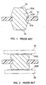
- Fig. 1 shows an example which comprises a
support member 51 of dielectric material and aconductive member 52 with upper and lowerconic surfaces 52A attached thereto by integral molding. The upper and lower flat end faces 53 and 54 make elastic contact with the circuit portions of connection objects. The number ofconductive members 52 provided on thesupport member 51 corresponds to the number of circuit portions of the connection objects. - In Fig. 2, two connection objects or
circuit boards support member 51. Thecircuit boards circuit portions contact faces conductive member 52. Thus, the twocircuit portions circuit boards conductive member 52 and short-circuited via theconductive member 52. - However, the above conventional intermediate electrical connector provides no satisfactory amount of elastic deformation of the
conductive member 52. Since theconductive member 52 increases in diameter from the upper and lower contact faces 53 and 54 to thesupport member 51 and held by the edges of thesupport aperture 51A, not only the pressure upon thecontact face 53 is distributed to the whole body but also a tension is produced on theconic surface 52 between theflange portion 52B and thecontact face 53 of theconductive member 52, providing no satisfactory amount of deformation. - When a number of conductive members are molded with a support member, there are variations in their heights. In addition, the circuit boards and the support member are warped so that more variations are added to the conductive members. Moreover, when the intermediate electrical connector receives an external force, the circuit boards momentarily moves in the compression direction of the conductive member, causing poor contact of the conductive member. Consequently, it is necessary for the conductive member to provide a sufficient amount of deformation to absorb the above variations. However, the above conventional connector provides no satisfactory amount of deformation, thus causing poor contact.
- The conductive elastomer has such a tendency that when compressed, its resistivity in the compression direction decreases. However, the amount of elastic deformation is so small that the contact resistance is high.
- When it is compressed, the conductive elastomer decreases in electrical resistance at the initial, stage but increases in electrical resistance beyond the initial stage. Thus, when it is compressed beyond the initial compression stage, the electrical characteristics deteriorates even though the mechanical contact is improved. In addition, if this high compression is applied to a number of conductive members, the combined force applied to the mating circuit boards is disadvantageously high.
- When a number of conductive members are molded with a support member, their heights are not equal. In addition, the circuit boards and the support member are warped to worsen the variations in the contact points of the conductive members. Moreover, when the intermediate electrical connector receives an external force, the circuit boards are moved in the compression direction of the conductive member, causing poor contact of the conductive member. Consequently, it is necessary for the conductive member to have sufficient elasticity to absorb the above variations. However, too much elasticity causes lower electrical characteristics described above.
- Accordingly, it is an object of the invention to provide an intermediate electrical connector with the conductive member having stable contact and lower contact resistance.
- The above object is achieved by the invention as claimed in
claim 1. - Embodiments of the invention will now be described by way of example with reference to the accompanying drawings, in which:
- Figs. 1 and 2 are sectional views of a conventional conductive member before and after deformation, respectively.
- Figs. 3 and 4 are sectional views of a conductive member according to an embodiment of the invention before and after deformation, respectively;
- Fig. 5 is a sectional view of a modified conductive member according to another embodiment of the invention;
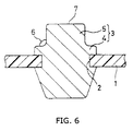
- Fig. 6 is a sectional view of a modified conductive member according to still another embodiment of the invention;
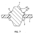
- Fig. 7 is a sectional view of a modified conductive member according to yet another embodiment of the invention;
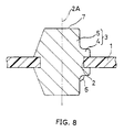
- Fig. 8 is a sectional view of a modified conductive member according to another embodiment of the invention;
- Fig. 9 is a sectional view of a modified conductive member according to still another embodiment of the invention;
- Figs. 10-13 are sectional views of a contact face according to various embodiments of the invention;
- Fig. 14 is a sectional view of a conductive member according to an embodiment of the invention;
- Fig. 15 is a sectional view of a modified conductive member according to another embodiment of the invention;
- Fig. 16 is a sectional view of a modified conductive member according to still another embodiment of the invention;
- Fig. 17 is a sectional view of a modified conductive member according to yet another embodiment of the invention;
- Fig. 18 is a sectional view of a conductive member according to an embodiment of the invention;
- Fig. 19 is a sectional view of a conductive member according to another embodiment of the invention;
- Fig. 20 is a perspective view of a conductive member according to still another embodiment of the invention;
- Fig. 21 is a perspective view of a conductive member according to yet another embodiment of the invention;
- Fig. 22 is a sectional view of a conductive member according to another embodiment of the invention;
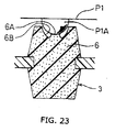
- Fig. 23 is a sectional view of the conductive member of Fig. 22, wherein it is being contacted;
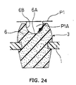
- Fig. 24 is a sectional view of the conductive member of Fig. 22, wherein it has been contacted;
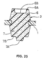
- Fig. 25 is a sectional view of a conductive member according to still another embodiment of the invention;
- Fig. 26 is a sectional view of a conductive member according to yet another embodiment of the invention; and
- Fig. 27 is a sectional view of a conductive member according to another embodiment of the invention; and
- Fig. 28 is a sectional view of a conductive member according to still another embodiment of the invention.
-
- In Fig. 3, a
support plate 1 is made of dielectric material. A plurality ofsupport apertures 2 having an inside diameter D1 are provided in thesupport plate 1, and a plurality ofconductive members 3 are attached thereto by integral molding such that eachconductive member 3 is held by the circumferential edges of eachsupport aperture 2. Preferred examples of the dielectric material include films of polyimide, polyester, and polyamide - The
conductive member 3 is made by mixing an elastic polymeric material with a conductive powder or particles. Preferred examples of the elastic polymers are silicone rubber, polybutadiene rubber, natural rubber, polyisoprene, styrene-butadiene copolymer rubber, acrylonitrile-butadiene copolymer rubber, ethylene-propylene copolymer rubber, urethane rubber, polyester rubbers, chloroprene rubber, epichlorohydrin rubber, and soft liquid epoxy rubber. Examples of the conductive powder or particles mixed with the elastic polymeric material include one or more of powder, granules, chips, flakes, and amorphous materials of gold, silver, nickel, copper, tin, aluminum, palladium, and carbon. Especially, flakes of silver are preferred. It is preferred that silver powder is treated with an organic silicon compound. - The
conductive member 3 has a retention section 4 and an elastic protrudedsection 5. The retention section 4 is brought into contact with the inside wall of thesupport aperture 2 and the upper and lower surfaces of thesupport plate 1 so as to cover the edges of thesupport aperture 2 of the inside diameter D1. The protrudedsection 5 hasshoulder portions 6 next to the retention section 4 and takes a cylindrical form having an outside diameter D2 and flat contact faces 7 at opposite ends. The outside diameter D2 is smaller than the inside diameter D1 of thesupport aperture 2 so that theprotruded section 5 is situated within radial range of theirsupport aperture 2. Theshoulder portions 6 are rounded as shown by R in the figure. - The intermediate electrical connector operates as follows.
- In Fig. 4, a pair of connection objects or
circuit boards support plate 1 and fixed at predetermined positions by proper means. Thecircuit boards circuit portions conductive member 3 when thecircuit boards - Since the elastic protruded
section 5 is situated within the radial range of thesupport aperture 2, it is able to undergo large elastic deformation in the vertical direction regardless of the presence of the retention section 4. The amount of elastic deformation of the protrudedsection 5 is sufficiently large to absorb variations of theconductive members 3 and thecircuit boards conductive members 3 under satisfactory contact pressure. In addition, the large amount of compression of theconductive members 3 reduces the electrical resistance. - Various modifications will be described below.
- In Fig. 5, the
shoulder portions 6 are formed with tilted surfaces. - In Fig. 6, one
shoulder portion 6 is provided on one of the sides and a conic section is provided on the other side to produce the same effects on the side where the shoulder portion is provided. - In Fig. 7, the protruded
section 5 takes a pair of upward and downward conic shapes withshoulder portions 6 next to the retention section 4. - In Fig. 8, the shape on the right side of an
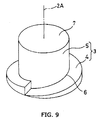
axis 2A is identical with the shape of Fig. 1 and the left side with the shape of Fig. 1 to produce a large amount of elastic deformation on the right side so that theconductive member 7 slide laterally relative to the circuit boards, producing the wiping effects. - In Fig. 9, the thickness of the retention section 4 changes in spiral manner to allow a large amount of elastic deformation of the protruded
section 5 and produce twisting movement around theaxis 2A, thereby producing the wiping effects relative to the circuit boards. - In Fig. 10, the
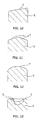
contact face 7 is tilted to produce the wiping effects. - In Fig. 11, the
contact face 7 has a conical surface to reduce the contact area with a mating object, which is prone to corrosion, so as to increase the Hertz stress and ensure the contact stability. - These effects also are produced by a convex
curved surface 7 as shown in Fig. 12. - In Fig. 13, a
concave surface 7 is provided on the contact area to produce the suction effects, thereby assuring firm contact. The depth of theconcave surface 7 is determined to match the solder ball or the like of a mating object as shown by phantom line. If the contact surface is provided with many fine projections, the wiping effects are produced at random. - As has been described above, according to one aspect of the invention, the conductive member is made of conductive elastomer so as to have a retention section for engagement with the edges of a support aperture of a support plate and an elastic protruded section extending from the retention section in the direction of thickness of the support plate. The retention section has flange portions extending in the radial direction of the support aperture. The elastic protruded section has a pair of contact portions for elastic contact with the circuit portions of connection objects. There are provided shoulder portions between the protruded section and the retention section. The diameter of the shoulder portions is smaller than the diameter of the support aperture so that upon contact with connection objects, the elastic protruded section is able to undergo large elastic deformation regardless of the presence of the retention section, thereby providing a sufficient amount of deformation to absorb variations of the conductive members and connection objects to thereby ensure stable connections. In addition, the large amount of compression reduces the contact resistance of the conductive members, thereby providing good electrical connections.
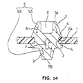
- In Fig. 14, a
support plate 1 is made of dielectric material. A plurality ofsupport apertures 2 having an inside diameter D1 are provided in thesupport plate 1, and a plurality ofconductive members 3 are attached thereto by integral molding such that eachconductive member 3 is held by thecircumferential edges 2A of eachsupport aperture 2. Preferred examples of the dielectric material include films of polyimide, polyester, and polyamide - The
conductive member 3 is made by mixing elastic polymeric material with conductive powder or particles. Preferred examples of the elastic polymers are silicone rubber, polybutadiene rubber, natural rubber, polyisoprene, styrene-butadiene copolymer rubber, acrylonitrile-butadiene copolymer rubber, ethylene-propylene copolymer rubber, urethane rubber, polyester rubbers, chloroprene rubber, epichlorohydrin rubber, and soft liquid epoxy rubber. - Examples of the conductive powder or particles ixed with the elastic polymeric material include one or more of powder, granules, chips, flakes, and amorphous materials of gold, silver, nickel, copper, tin, aluminum, palladium, and carbon. Especially, flakes of silver are preferred. It is preferred that silver powder is treated with an organic silicon compound.
- The
conductive member 3 has a retention section 4 and anelastic protruded section 5. The retention section 4 is brought into contact with the inside wall of thesupport aperture 2 and the upper and lower surfaces of thesupport plate 1 so as to cover theedges 2A of thesupport aperture 2. Theconductive member 3 is integrally molded with thesupport member 1. The protrudedsection 5 has upward and downward extendingsections section 5A has a conic side and a displacement means orrecess 6 at the top surface, forming anannular bearing face 7A. - The downward extending
section 5B has a conic side having an outside diameter smaller than the outside diameter of the upward extendingsection 5A but substantially equal to the inside diameter of thedisplacement recess 6 and is situated at a position corresponding to thedisplacement recess 6. Also, it has acircular bearing face 7B having a diameter substantially equal to the inside diameter of thedisplacement recess 6. - The intermediate electrical connector operates as follows.
- In Fig. 14, a pair of connection objects or circuit boards are provided on both sides of the
support plate 1 and fixed at predetermined positions by proper means. The circuit boards have circuit portions, respectively, which are pressed against the bearing faces 7A and 7B of theconductive member 3 when the circuit boards are situated at the predetermined positions. - The upward extending
section 5A is compressed in the direction of an arrow A by the pressure on thebearing face 7A while the downward extendingsection 5B is compressed in the direction of an arrow B by the pressure on thebearing face 7B and is displaced into thedisplacement recess 6 indicated by an arrow F. Consequently, the downward extendingsection 5B is moved by the sum of the compressed length and displaced distance. Thus, even if the compressed length is small, the total amount of movement is large. The contact pressure is smaller than the contact pressure under which the conventional conductive member is moved by the same amount. - The amount of movement of the elastic protruded
section 5 is so large that even if there are variations between the bearing faces 7A and 7B of a number ofconductive members 3 and the circuit portions of connection objects, such variations are absorbed satisfactorily. Consequently, under light contact pressures, good contacts are ensured for all of theconductive members 3. The compression of theconductive members 3 is so small that the electrical resistance is low, improving the electrical characteristics. - Various modifications will be described below.
- In Fig. 15, the upward and downward extending
sections central axes spaces sections conductive member 3 is tilted because of its asymmetric shape, increasing the amount of movement. - In Fig. 16, the
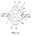
conductive member 3 is held by the central portion in contrast to the above modification wherein theconductive member 3 is held by engagement between the retention flanges 4 and the edges of a support aperture. The inside diameter of thesupport aperture 2 is larger than the outside diameter of theconductive member 3. Abridge portion 1A diametrically extends across thesupport aperture 2. Theconductive member 3 is spaced from the side face of thesupport aperture 2 and held by thebridge portion 1A. Since the circumferential face of theconductive member 3 is not fixed, it is easy for theconductive member 3 to tilt, thus increasing the amount of movement. - In Fig. 17, a pair of displacement means or
cavities conductive member 3. Any number and/or size of the displacement cavities may be provided as far as it is effective for the elastic protruded sections to move. That is, the elastic protruded sections may be made of foam rubber to produce the effects. - As has been described above, according to another aspect of the invention, the conductive member is made of conductive elastomer so as to have a retention section for engagement with a support plate and an elastic protruded section extending from the retention section in the direction of thickness of the support plate. A displacement means is provided in the conductive member to allow the elastic protruded section to displace so that the bearing face of the protruded section can move to a large extent, thereby providing a sufficient amount of movement to absorb variations in relative positions between the conductive members and connection objects or momentary movement of connection objects, ensuring a stable contact. Since the amount of compression is limited to the proper level, the conductive member maintains the low contact resistance, ensuring the good electrical characteristics.
- In Fig. 18, a
support plate 1 is made of dielectric material. A plurality ofsupport apertures 2 are provided in thesupport plate 1, and a plurality ofconductive members 3 are attached thereto by integral molding. Preferred examples of the dielectric material are films of polyimide, polyester, and polyamide. - The
conductive member 3 is made of mixing elastic polymeric material with conductive powder or particles. Preferred examples of the elastic polymers are silicone rubber, polybutadiene rubber, natural rubber, polyisoprene, styrene-butadiene copolymer rubber, acrylonitrile-butadiene copolymer rubber, ethylene-propylene copolymer rubber, urethane rubber, polyester rubbers, chloroprene rubber, epichlorohydrin rubber, and soft liquid epoxy rubber. - Examples of the conductive powder or particles mixed with the elastic polymeric material include one or more of powder, granules, chips, flakes, and amorphous materials of gold, silver, nickel, copper, tin, aluminum, palladium, and carbon. Especially, flakes of silver are preferred. It is preferred that silver powder is treated with an organic silicon compound.
- The
conductive member 3 has retention sections 4 and elastic protrudedsections 5. The retention sections 4 are brought into contact with the inside wall of thesupport aperture 2 and the upper and lower surfaces of thesupport plate 1 so as to cover the edges of thesupport aperture 2. Such a retention structure is obtained by integrally molding theconductive members 3 with thesupport plate 1. Theprotruded sections 5 consists of upper and lowerconic sections - The lower
conic section 7 has a pedestal section with a lowerflat contact face 7A while, according to the invention, the upperconic section 6 has a double pedestal sections with first and second contact faces 6A and 6B. The first and second contact faces 6A have a flat surface, respectively, to match the flat circuit portions P1A and P2A of circuit boards P1 and P2, respectively, but may have a curbed or tilted surface. According to the invention, one of the upper and lower conic sections has a plurality of contact surfaces which are made in the form of a step. - The distance between the first and second contact faces 6A and 6B is determined by the amount of compression caused by the circuit boards or connection objects. When the
conductive member 3 is compressed by the upper circuit board P1, thefirst contact face 6A receives the pressure for compression up to the distance , where thesecond contact face 6B starts contact for compression. The is determined at such a point that the electrical resistance of theconductive member 3 starts to rise under the conditions that only thefirst contact face 6A receives the compression. - The intermediate connector operates as follows.
- In Fig. 18, a pair of connection objects or circuit boards P1 and P2 are provided and fixed by proper means on upper and lower sides of the
support plate 1 so as to compress theconductor member 3. The circuit boards P1 and P2 have a circuit portion P1A or P2A, respectively, so that when they are fixed at the predetermined positions, the circuit portions P1A and P2A press the contact faces 6A, 6B, and 7A of theconductive member 3, respectively. - The
first contact face 6A receives the pressure from the circuit board P1 so that the upper protrudedsection 6 is compressed in the direction of an arrow A. The electrical resistance decreases in the initial stage but starts to increase when the amount of compression reechoes the value . When theconductive member 3 is further compressed, thesecond contact face 6B is brought into contact with the connection object P1 so that the contact area increases so much that the electrical resistance decreases. The position of the connection object P1 is determined at a position where the amount of compression is set before the electrical resistance increases after the initial decrease. - The
contact face 7A of thelower protruded section 7 is brought into contact with the lower connection object P2 under a predetermined contact pressure. Thus, the circuit portions P1A and P2A of the connection objects P1 and P2 are connected to each other with a low electrical resistance and a large amount of movement because of the first and second contact faces 6A and 6B of the upper protruded section. Consequently, variations in the contact positions due to variations in the circuit component positions, warp of the support plate, and dimensions of the conductive member are absorbed satisfactorily while the good electrical characteristics are maintained. The lower protrudedsection 7 may be made so as to have the same structure as the upper protrudedsection 6. - Various modifications will be described below.
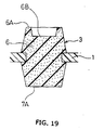
- In Fig. 19, a recess is provided at the center of a top face so as to form first and second contact faces 6A and 6B. The area ratio and the distance between the contact faces 6A and 6B are determined such that the second contact face starts to contact the connection object when the electrical resistance at the
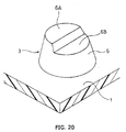
first contact face 6A starts to increase with increase of the compression. - In Fig. 20, the top face of the upper protruded
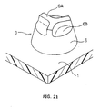
section 6 is divided into first and second contact faces 6A and 6B by a diametric line. - In Fig. 21, the
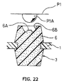
first contact face 6A extends in radial directions, with the remaining area made as thesecond contact face 6B. - In Fig. 22, where the circuit portion P1A of a connection object P1 is hemispheric, it is preferred that the
second contact face 6B has a concave surface to match the hemispheric circuit portion P1A while thefirst contact face 6A is flat. - In Fig. 23, the circuit portion P1A of a connection object P1 first makes contact with the
first contact face 6A and thesecond contact face 6B as shown in Fig. 24. - In Fig. 25, the upper protruded
section 6 has the same structure as that of Fig. 19 while thelower protruded section 7 has the same structure as that of Fig. 18. At the initial compression stage, the amount of compression of thefirst contact face 7A is absorbed by the concavesecond contact face 6B because thefirst contact face 7A is situated at a position corresponding to the concavesecond contact face 6B so that theconductor member 3 as a whole is not compressed very much. That is, a small force to compress is able to provide the above displacement of thefirst contact face 7A. - In Fig. 26, where the circuit portion of a connection object is flat, the
first contact face 6A is flat and parallel to thesupport plate 1 while thesecond contact face 6B is sloped. Both of the contact faces 6A and 6B make successive contacts with the circuit portion to produce the effects described above according to the invention. Alternatively, the sloped face may be curved. - The above two stepped contact faces with the circuit portion of a connection object may be three or more stepped contacts. The various contact faces may be provided on both or either of the upper and lower protruded sections.
- In Fig. 27, the
conductive member 3 has upper and lower flat contact faces 6A and 6B while the upper and lower circuit portions P1A and P2A of connection objects P1 and P2 have raised and indented areas, respectively, so that theconductive member 3 is compressed in stepped manner to produce the same effects as described above. It is sufficient that the circuit portion of either upper or lower contact object is provided with either raised or indented configuration. - In Fig. 28, the
conductive member 3, which has a configuration similar to the upper half of theconductive member 3 of Fig. 18, is provided on acircuit portion 1A of thesupport member 1. It makes successive contacts with the circuit portion P1A of a connection object P1 in the same manner as the conductive member of Fig. 18. Such a conductive member as this may be applied to any of the connection methods described in Figs. 18 through 28. - As has been described above, according to still another aspect of the invention, a plurality of contact faces are provided so that the contact area increases in stepped manner as the conductive member is compressed. Consequently, not only the increase in electrical resistance with the increase in compression is prevented but also large amounts of displacement of the contact faces are assured so that variations in distance between the conductive members and the connection objects are absorbed and the contacts are so stable that the electrical characteristics are improved.
Claims (25)
- An intermediate electrical connector comprising:a support plate which is made of a dielectric material and has at least one support aperture having an inside diameter; andat least one conductive member provided through said support aperture to short-circuit circuit portions of connection objects; said conductive member being made of a conductive elastomer and comprising:a retention section with flange portions for engage with said support aperture to attach said conductive member to said support plate; andan elastic protruded section extending from said retention section in a direction of thickness of said support plate to form at opposite ends contact faces for elastic contact with said circuit portions of said connection objects and adjacent to said retention section shoulder portions having an outside diameter which is smaller than said inside diameter of said support aperture.
- An intermediate electrical connector according to claim 1, wherein said conductive member has a longitudinal section which is symmetric relative to an axis of said conductive member.
- An intermediate electrical connector according to claim 1, wherein said conductive member has a longitudinal section which is asymmetric relative to an axis of said conductive member.
- An intermediate electrical connector according to claim 3, wherein said longitudinal section of said conductive member changes in a circumferential direction.
- An intermediate electrical connector according to one of claim 1, wherein said protruded section has a cylindrical surface.
- An intermediate electrical connector according to one of claim 1, wherein said protruded section has a conic surface.
- An intermediate electrical connector according to claim 2, wherein said contact faces each have a flat surface at right angles to said axis.
- An intermediate electrical connector according to claim 2, wherein said contact faces each have a convex or concave surface.
- An intermediate electrical connector according to claim 3, wherein said contact faces each have a tilted surface.
- An intermediate electrical connector comprising:a support plate which is made of a dielectric material and has at least one support aperture; andat least one conductive member provided through said support aperture to short-circuit circuit portions of connection objects; said conductive member being made of a conductive elastomer and comprising:a retention section for engage with said support aperture to attach said conductive member to said support plate; andan elastic protruded section extending from said retention section in a direction of thickness of said support plate to form at opposite ends a pair of bearing faces for elastic contact with said circuit portions of said connection objects; anddisplacement means for allowing said elastic protruded section to undergo elastic displacement.
- An intermediate electrical connector according to claim 10, wherein said displacement means is provided between a face opposite to said bearing face and one of said connection objects.
- An intermediate electrical connector according to claim 10, wherein said displacement means is a cavity provided within said conductive member.
- An intermediate electrical connector according to claim 10, wherein said retention section of said conductive member is held by a circumferential edge of said support aperture.
- An intermediate electrical connector according to one of claims 10, wherein said conductive member is held by a bridge portion extending across said support aperture.
- An intermediate electrical connector comprising:a support plate made of a dielectric material so as to have a support aperture;a conductive member supported by said support plate and made of a conductive elastomer so as to have at opposite ends a pair of contact faces for contact with a pair of connection objects provided on opposite sides of said support plate to short-circuit circuit portions of said connection objects, wherein at least one of said contact faces has at least first and second contact sections which make successive contacts with one of said circuit portions of said connection objects.
- An intermediate electrical connector according to claim 15, wherein said first contact section is substantially parallel to said circuit portion of said connection object while said second contact section is provided closer to said support plate than said first contact section.
- An intermediate electrical connector according to claim 15, wherein said first contact section is provided at a center of said contact face while said second contact section is provided around said first contact section.
- An intermediate electrical connector according to claim 16, wherein said first contact section is provided at a periphery of said contact face while said second contact section is provided at a center of said contact face.
- An intermediate electrical connector according to claim 16, wherein said first contact section is provided at a portion of periphery while said second contact section is provided adjacent to said first contact section.
- An intermediate electrical connector according to claim 16, wherein said first contact section extends radially on said contact face while said second contact section is provided at a remaining area of said contact face.
- An intermediate electrical connector according to claim 16, wherein said contact face has a generally concave surface to match a convex surface of said circuit portion of said connection object, said concave surface having a raised portion to form said first contact section and a remaining portion to form said second contact section.
- An intermediate electrical connector according to claim 16, wherein said first contact section is parallel to said circuit portion of said connection object while said second contact section is tilted with respect to said first contact section.
- An electrical connection system comprising:a support plate made of a dielectric material so as to have a support aperture;a conductive member supported by said support plate made of a conductive elastomer so as to have at opposite ends a pair of contact faces for contact with circuit portions of a pair of connection objects provided on opposite sides of said support plate to short-circuit said circuit portions; wherein at least one of said contact faces has at least first and second contact sections which make successive contacts with one of said circuit portions.
- An electrical connection system comprising:a support plate made of a dielectric materialan electric circuit provided on one face of said support plate;a conductive member provided on said electric circuit and made of a conductive elastomer so as to have at an end opposite to said electric circuit a contact face with at least first and second contact sections which make successive contacts with a circuit portion of a connection object to short-circuit said electric circuit to said circuit portion of said connection object.
- An electrical connection system comprising:a support plate made of a dielectric material;an electrical circuit provided on a face of said support plate;a conductive member made of a conductive elastomer so as to have a contact face for contact with a circuit portion of a connection object to short-circuit said electrical circuit to said circuit portion of said connection object, wherein said electrical circuit has at least first and second contacts sections which make successive contacts with said contact face of said conductive member.
Applications Claiming Priority (6)
| Application Number | Priority Date | Filing Date | Title |
|---|---|---|---|
| JP12791299 | 1999-05-10 | ||
| JP12791299A JP3350479B2 (en) | 1999-05-10 | 1999-05-10 | Intermediate electrical connector |
| JP26963299A JP2001094275A (en) | 1999-11-24 | 1999-09-24 | Intermediate electric connector |
| JP26963299 | 1999-11-24 | ||
| JP2000007307 | 2000-01-17 | ||
| JP2000007307A JP2001203016A (en) | 2000-01-17 | 2000-01-17 | Intermediate electric connector |
Publications (2)
| Publication Number | Publication Date |
|---|---|
| EP1061608A2 true EP1061608A2 (en) | 2000-12-20 |
| EP1061608A3 EP1061608A3 (en) | 2002-10-02 |
Family
ID=27315645
Family Applications (1)
| Application Number | Title | Priority Date | Filing Date |
|---|---|---|---|
| EP00109893A Withdrawn EP1061608A3 (en) | 1999-05-10 | 2000-05-10 | Board to board electrical connectors |
Country Status (2)
| Country | Link |
|---|---|
| US (1) | US6280207B1 (en) |
| EP (1) | EP1061608A3 (en) |
Cited By (6)
| Publication number | Priority date | Publication date | Assignee | Title |
|---|---|---|---|---|
| WO2003045123A1 (en) * | 2001-11-16 | 2003-05-30 | R-Tec Corporation | Interposer |
| WO2004038433A1 (en) | 2002-10-28 | 2004-05-06 | Jsr Corporation | Sheet-form connector and production method and application therefor |
| WO2004040762A1 (en) * | 2002-10-29 | 2004-05-13 | BSH Bosch und Siemens Hausgeräte GmbH | Capacitive proximity sensor and/or contact sensor, and electrically conductive plastic member for such a sensor |
| EP1416636A3 (en) * | 2002-10-31 | 2005-08-31 | E.G.O. Elektro-Gerätebau GmbH | Sensor element for a capacitive touch switch with an electrically conductive element and method of producing the same |
| EP1577974A2 (en) * | 2004-03-19 | 2005-09-21 | Hirschmann Electronics GmbH & Co. KG | Device for contacting an antenna structure, made by multi-component injection moulding |
| DE102007054524A1 (en) | 2007-11-07 | 2009-02-26 | E.G.O. Control Systems Gmbh | Body structure for a flexible body like a sensor element applied to a printed circuit board fits in a holding/mounting device with a channel-type retaining device for the flexible body |
Families Citing this family (16)
| Publication number | Priority date | Publication date | Assignee | Title |
|---|---|---|---|---|
| EP1340289A4 (en) * | 2000-12-05 | 2006-03-22 | Aprion Digital Ltd | Board integrated resilient contact elements array and method of fabrication |
| JP4139385B2 (en) * | 2002-05-28 | 2008-08-27 | モレックス インコーポレーテッド | Connector transport assembly |
| US6799977B2 (en) * | 2002-07-11 | 2004-10-05 | Hewlett-Packard Development Company, L.P. | Socket having foam metal contacts |
| TW547771U (en) * | 2002-07-23 | 2003-08-11 | Via Tech Inc | Elastic electrical contact package structure |
| US6786736B2 (en) * | 2002-08-23 | 2004-09-07 | Artesyn Technologies, Inc. | Surface mount interconnect and device including same |
| DE20321550U1 (en) * | 2003-08-11 | 2007-12-20 | Hirschmann Electronics Gmbh & Co. Kg | Elastic contact elements for clipping |
| US6994570B2 (en) * | 2004-01-28 | 2006-02-07 | International Business Machines Corporation | High performance interposer for a chip package using deformable button contacts |
| US7442049B2 (en) * | 2005-02-09 | 2008-10-28 | International Business Machines Corporation | Electrical connecting device and method of forming same |
| US7059867B1 (en) * | 2005-03-30 | 2006-06-13 | Artesyn Technologies, Inc. | High density multi-lead surface mount interconnect and devices including same |
| JP5064205B2 (en) * | 2007-12-27 | 2012-10-31 | タイコエレクトロニクスジャパン合同会社 | Contacts and interposers |
| US9153890B2 (en) * | 2012-04-18 | 2015-10-06 | R+DCircuits, Inc. | Singulated elastomer electrical contactor for high performance interconnect systems and method for the same |
| US9853383B2 (en) * | 2015-09-11 | 2017-12-26 | General Electric Company | Conductive polymer contacts for surface mount technology connectors |
| EP3174166B1 (en) * | 2015-11-25 | 2018-11-14 | ODU GmbH & Co KG. | Damping element for providing axial damping in a plug-in connector, plug-in connector and method for forming a plug-in connector |
| US10276402B2 (en) * | 2016-03-21 | 2019-04-30 | Taiwan Semiconductor Manufacturing Co., Ltd. | Semiconductor package and manufacturing process thereof |
| IT201700100522A1 (en) * | 2017-09-07 | 2019-03-07 | Technoprobe Spa | Interface element for an electronic device test device and its manufacturing method |
| JP2022139728A (en) * | 2021-03-12 | 2022-09-26 | パナソニックIpマネジメント株式会社 | Interboard connection structure and power conversion device |
Citations (5)
| Publication number | Priority date | Publication date | Assignee | Title |
|---|---|---|---|---|
| DE2407738A1 (en) * | 1973-02-21 | 1974-08-22 | Electrovac | Connector for liq. crystal leads to circuit board - uses intermediate connector block of conductive PVC or silicon rubber |
| US3971610A (en) * | 1974-05-10 | 1976-07-27 | Technical Wire Products, Inc. | Conductive elastomeric contacts and connectors |
| US4050756A (en) * | 1975-12-22 | 1977-09-27 | International Telephone And Telegraph Corporation | Conductive elastomer connector and method of making same |
| US4240198A (en) * | 1979-02-21 | 1980-12-23 | International Telephone And Telegraph Corporation | Method of making conductive elastomer connector |
| US5738530A (en) * | 1996-05-28 | 1998-04-14 | Packard Hughes Interconnect Company | Contact pad having metallically anchored elastomeric electrical contacts |
Family Cites Families (4)
| Publication number | Priority date | Publication date | Assignee | Title |
|---|---|---|---|---|
| SU1187229A1 (en) * | 1982-12-20 | 1985-10-23 | Akopyan Robert A | Electric connector |
| US5163834A (en) * | 1990-12-17 | 1992-11-17 | International Business Machines Corporation | High density connector |
| US6056557A (en) * | 1998-04-08 | 2000-05-02 | Thomas & Betts International, Inc. | Board to board interconnect |
| JP2901603B1 (en) * | 1998-07-01 | 1999-06-07 | ユニテクノ株式会社 | Electronic component conductive sheet |
-
2000
- 2000-05-10 EP EP00109893A patent/EP1061608A3/en not_active Withdrawn
- 2000-05-10 US US09/567,985 patent/US6280207B1/en not_active Expired - Fee Related
Patent Citations (5)
| Publication number | Priority date | Publication date | Assignee | Title |
|---|---|---|---|---|
| DE2407738A1 (en) * | 1973-02-21 | 1974-08-22 | Electrovac | Connector for liq. crystal leads to circuit board - uses intermediate connector block of conductive PVC or silicon rubber |
| US3971610A (en) * | 1974-05-10 | 1976-07-27 | Technical Wire Products, Inc. | Conductive elastomeric contacts and connectors |
| US4050756A (en) * | 1975-12-22 | 1977-09-27 | International Telephone And Telegraph Corporation | Conductive elastomer connector and method of making same |
| US4240198A (en) * | 1979-02-21 | 1980-12-23 | International Telephone And Telegraph Corporation | Method of making conductive elastomer connector |
| US5738530A (en) * | 1996-05-28 | 1998-04-14 | Packard Hughes Interconnect Company | Contact pad having metallically anchored elastomeric electrical contacts |
Cited By (11)
| Publication number | Priority date | Publication date | Assignee | Title |
|---|---|---|---|---|
| WO2003045123A1 (en) * | 2001-11-16 | 2003-05-30 | R-Tec Corporation | Interposer |
| WO2003045122A1 (en) * | 2001-11-16 | 2003-05-30 | R-Tec Corporation | Method of making an interposer |
| WO2004038433A1 (en) | 2002-10-28 | 2004-05-06 | Jsr Corporation | Sheet-form connector and production method and application therefor |
| EP1503216A1 (en) * | 2002-10-28 | 2005-02-02 | JSR Corporation | Sheet-form connector and production method and application therefor |
| EP1503216A4 (en) * | 2002-10-28 | 2008-03-26 | Jsr Corp | Sheet-form connector and production method and application therefor |
| WO2004040762A1 (en) * | 2002-10-29 | 2004-05-13 | BSH Bosch und Siemens Hausgeräte GmbH | Capacitive proximity sensor and/or contact sensor, and electrically conductive plastic member for such a sensor |
| US7525062B2 (en) | 2002-10-29 | 2009-04-28 | Bsh Bosch Und Siemens Hausgeraete Gmbh | Capacitive proximity and/or contact sensor and electrically conductive plastic body for such a sensor |
| EP1416636A3 (en) * | 2002-10-31 | 2005-08-31 | E.G.O. Elektro-Gerätebau GmbH | Sensor element for a capacitive touch switch with an electrically conductive element and method of producing the same |
| EP1577974A2 (en) * | 2004-03-19 | 2005-09-21 | Hirschmann Electronics GmbH & Co. KG | Device for contacting an antenna structure, made by multi-component injection moulding |
| EP1577974A3 (en) * | 2004-03-19 | 2006-01-18 | Hirschmann Electronics GmbH & Co. KG | Device for contacting an antenna structure, made by multi-component injection moulding |
| DE102007054524A1 (en) | 2007-11-07 | 2009-02-26 | E.G.O. Control Systems Gmbh | Body structure for a flexible body like a sensor element applied to a printed circuit board fits in a holding/mounting device with a channel-type retaining device for the flexible body |
Also Published As
| Publication number | Publication date |
|---|---|
| EP1061608A3 (en) | 2002-10-02 |
| US6280207B1 (en) | 2001-08-28 |
Similar Documents
| Publication | Publication Date | Title |
|---|---|---|
| US6280207B1 (en) | Intermediate electrical connector | |
| US7390196B2 (en) | Connector, and portable terminal equipment including the connector | |
| US6776668B1 (en) | Low profile coaxial board-to-board connector | |
| US7473104B1 (en) | Electrical connector having improved two-half contacts for land grid array socket | |
| US8052454B2 (en) | Electrical connector with improved feature for securing solder ball thereon | |
| EP1797619B1 (en) | Contact for electronic devices | |
| CN101621161B (en) | Both-face connection type connector | |
| US6902410B2 (en) | Contact unit and socket for electrical parts | |
| US20080180125A1 (en) | Contact Probe And Socket For Testing Semiconductor Chips | |
| CN1917289A (en) | Electrical interconnect system utilizing nonconductive elastomeric elements and continuous conductive elements | |
| US6790057B2 (en) | Conductive elastomeric contact system with anti-overstress columns | |
| CN111149003B (en) | Conductive contact and anisotropic conductive sheet having the same | |
| JP2000200636A (en) | Conductive elastomer mutual connector | |
| US7833020B1 (en) | Electrical connector with low profile terminal | |
| US20050204538A1 (en) | Contact and method for making same | |
| US20120003845A1 (en) | Split ring terminal assembly | |
| US20030008535A1 (en) | Electrical contact and electrical connection device using same | |
| US20090156022A1 (en) | Contact Member and Connector Including Same | |
| US6565364B1 (en) | Wafer formed with CSP device and test socket of BGA device | |
| US20050009386A1 (en) | Compliant electrical probe device incorporating anisotropically conductive elastomer and flexible circuits | |
| US7445463B2 (en) | Land grid array electrical connector | |
| JP3350479B2 (en) | Intermediate electrical connector | |
| US20110053426A1 (en) | Lower profile electrical contact and electrical socket using the same | |
| US11693027B2 (en) | Conductive particle and testing socket comprising the same | |
| CN1319217C (en) | Pressure contact connector of cell phone and connection structure of the connector |
Legal Events
| Date | Code | Title | Description |
|---|---|---|---|
| PUAI | Public reference made under article 153(3) epc to a published international application that has entered the european phase |
Free format text: ORIGINAL CODE: 0009012 |
|
| AK | Designated contracting states |
Kind code of ref document: A2 Designated state(s): AT BE CH CY DE DK ES FI FR GB GR IE IT LI LU MC NL PT SE |
|
| AX | Request for extension of the european patent |
Free format text: AL;LT;LV;MK;RO;SI |
|
| RIC1 | Information provided on ipc code assigned before grant |
Free format text: 7H 01R 12/22 A, 7H 02B 1/00 B, 7H 01R 13/24 B, 7H 05K 1/14 B, 7H 01R 12/04 B, 7H 05K 3/36 B, 7H 01R 12/32 B |
|
| PUAL | Search report despatched |
Free format text: ORIGINAL CODE: 0009013 |
|
| AK | Designated contracting states |
Kind code of ref document: A3 Designated state(s): AT BE CH CY DE DK ES FI FR GB GR IE IT LI LU MC NL PT SE |
|
| AX | Request for extension of the european patent |
Free format text: AL;LT;LV;MK;RO;SI |
|
| AKX | Designation fees paid | ||
| REG | Reference to a national code |
Ref country code: DE Ref legal event code: 8566 |
|
| STAA | Information on the status of an ep patent application or granted ep patent |
Free format text: STATUS: THE APPLICATION IS DEEMED TO BE WITHDRAWN |
|
| 18D | Application deemed to be withdrawn |
Effective date: 20030403 |