EP1061111A1 - Abrasive composition for polishing semiconductor device and process for producing semiconductor device with the same - Google Patents
Abrasive composition for polishing semiconductor device and process for producing semiconductor device with the same Download PDFInfo
- Publication number
- EP1061111A1 EP1061111A1 EP99906467A EP99906467A EP1061111A1 EP 1061111 A1 EP1061111 A1 EP 1061111A1 EP 99906467 A EP99906467 A EP 99906467A EP 99906467 A EP99906467 A EP 99906467A EP 1061111 A1 EP1061111 A1 EP 1061111A1
- Authority
- EP
- European Patent Office
- Prior art keywords
- polishing
- semiconductor device
- atom
- silicon nitride
- nitride layer
- Prior art date
- Legal status (The legal status is an assumption and is not a legal conclusion. Google has not performed a legal analysis and makes no representation as to the accuracy of the status listed.)
- Granted
Links
- VKBAWGJUOGJQBW-UHFFFAOYSA-N C=C1C=C(C(CCC2)[N+]([O-])=C)C2=CC1 Chemical compound C=C1C=C(C(CCC2)[N+]([O-])=C)C2=CC1 VKBAWGJUOGJQBW-UHFFFAOYSA-N 0.000 description 1
Images

Classifications
-
- C—CHEMISTRY; METALLURGY
- C09—DYES; PAINTS; POLISHES; NATURAL RESINS; ADHESIVES; COMPOSITIONS NOT OTHERWISE PROVIDED FOR; APPLICATIONS OF MATERIALS NOT OTHERWISE PROVIDED FOR
- C09K—MATERIALS FOR MISCELLANEOUS APPLICATIONS, NOT PROVIDED FOR ELSEWHERE
- C09K3/00—Materials not provided for elsewhere
- C09K3/14—Anti-slip materials; Abrasives
-
- H—ELECTRICITY
- H01—ELECTRIC ELEMENTS
- H01L—SEMICONDUCTOR DEVICES NOT COVERED BY CLASS H10
- H01L21/00—Processes or apparatus adapted for the manufacture or treatment of semiconductor or solid state devices or of parts thereof
- H01L21/02—Manufacture or treatment of semiconductor devices or of parts thereof
- H01L21/04—Manufacture or treatment of semiconductor devices or of parts thereof the devices having at least one potential-jump barrier or surface barrier, e.g. PN junction, depletion layer or carrier concentration layer
- H01L21/18—Manufacture or treatment of semiconductor devices or of parts thereof the devices having at least one potential-jump barrier or surface barrier, e.g. PN junction, depletion layer or carrier concentration layer the devices having semiconductor bodies comprising elements of Group IV of the Periodic System or AIIIBV compounds with or without impurities, e.g. doping materials
- H01L21/30—Treatment of semiconductor bodies using processes or apparatus not provided for in groups H01L21/20 - H01L21/26
- H01L21/31—Treatment of semiconductor bodies using processes or apparatus not provided for in groups H01L21/20 - H01L21/26 to form insulating layers thereon, e.g. for masking or by using photolithographic techniques; After treatment of these layers; Selection of materials for these layers
- H01L21/3105—After-treatment
- H01L21/31051—Planarisation of the insulating layers
- H01L21/31053—Planarisation of the insulating layers involving a dielectric removal step
-
- C—CHEMISTRY; METALLURGY
- C09—DYES; PAINTS; POLISHES; NATURAL RESINS; ADHESIVES; COMPOSITIONS NOT OTHERWISE PROVIDED FOR; APPLICATIONS OF MATERIALS NOT OTHERWISE PROVIDED FOR
- C09K—MATERIALS FOR MISCELLANEOUS APPLICATIONS, NOT PROVIDED FOR ELSEWHERE
- C09K3/00—Materials not provided for elsewhere
- C09K3/14—Anti-slip materials; Abrasives
- C09K3/1454—Abrasive powders, suspensions and pastes for polishing
- C09K3/1463—Aqueous liquid suspensions
Definitions
- the present invention relates to an abrasive composition for polishing a semiconductor device, more specifically, to an abrasive composition for use in element isolation of a semiconductor device by the shallow trench isolation process, as well as a process for manufacturing a semiconductor device using said abrasive composition.
- a silicon nitride layer is formed as a lower layer of the oxide layer to be polished, the silicone nitride layer is used as the stopper in the polishing, the surface to be planarized is polished to give uniform and exact removed thickness, and the polishing is finished when a predetermined thickness removed is reached.
- JP-A-9-194823 describes a composition using silicon nitride, silicon carbide or graphite as the particulate abrasive and JP-A-9-208933 describes an abrasive composition comprising silicone nitride fine powder having added thereto an acid such as gluconic acid.
- abrasive compositions contain an abrasive having high hardness and certainly ensure a high polishing rate, however, they are disadvantageous in that many scratches are generated on the polished surface and give rise to reduction in the performance of the semiconductor device.
- the above-described techniques are insufficient in the "selectivity ratio" which is a value obtained by dividing the polishing rate for an oxide layer by the polishing rate for a silicon nitride layer and shows how easy the oxide layer, in many cases, silicon dioxide layer is polished as compared with the silicon nitride stopper layer.
- the selection ratio is a value obtained by dividing the polishing rate for an oxide layer by the polishing rate for a silicon nitride layer and shows how easy the oxide layer, in many cases, silicon dioxide layer is polished as compared with the silicon nitride stopper layer.
- the object of the present invention is to provide an abrasive composition for polishing a semiconductor device, which can overcome the above-described problems.
- Another object of the present invention is to provide a semiconductor device, which have solved the above-described problems.
- an abrasive composition for polishing a semiconductor device in the shallow trench isolation process said composition mainly comprising water, cerium oxide powder and one or more water-soluble organic compound having at least one of a -COOH group, a -COOM X group (wherein M X is an atom or functional group capable of displacing a H atom to form a salt), a -SO 3 H group and a -SO 3 M Y group (wherein M Y represents an atom or functional group capable of displacing a H atom to form a salt).
- the abrasive composition for manufacturing a semiconductor device of the present invention (2) wherein the concentration of cerium oxide in the abrasive composition is from 0.1 to 10 wt% and the amount of the water-soluble organic compound added, in terms of the weight ratio to the cerium oxide, is from 0.001 to 20, and (3) wherein when a silicon nitride layer and a silicon oxide layer separately formed on a silicon substrate by the CVD method are independently polished under the same conditions, the ratio of the polishing rate for the former to that for the latter is 10 or more, the scratches on the polished surface can be significantly reduced and the value of the selectivity ratio can significantly increase.
- the present invention also provide a process for manufacturing a semiconductor device, comprising the steps of
- shallow trench isolation can be formed with reduced scratches on the polished surface and with a high controllability.
- the abrasive composition for polishing a semiconductor device of the present invention is first described.
- the cerium oxide fine powder used in the present invention is preferably in a high purity, specifically, the purity is preferably 99 wt% or more, more preferably 99.9 wt% or more. If the purity is less than this range, it is difficult to remove the impurity elements having adverse effects on the properties of the semiconductor from the surface of the semiconductor device even if the semiconductor device after the polishing is cleaned, as a result, defectives increase and the yield disadvantageously decreases.
- the average particle size of the cerium oxide fine powder is preferably from 0.01 to 1.0 ⁇ m, more preferably from 0.1 to 0.5 ⁇ m. If the average particle size is less than 0.01 ⁇ m, the polishing rate for the oxide layer, in many cases, silicon dioxide layer, is reduced, whereas if it exceeds 1.0 ⁇ m, fine scratches are readily generated on the polished surface.
- the primary particle size of cerium oxide is preferably from 0.005 to 0.5 ⁇ m, more preferably from 0.02 to 0.2 ⁇ m. If the primary particle size is less than 0.005 ⁇ m, the polishing rate for the oxide layer is extremely reduced and a sufficiently large selection ratio cannot be attained, whereas if it exceeds 0.5 ⁇ m, fine scratches are readily generated on the polished surface.
- the concentration of cerium oxide (fine powder) in the abrasive composition of the present invention depends on the polishing conditions such as working pressure, however, it is preferably from 0.1 to 10 wt%, more preferably from 0.3 to 5 wt%. If the concentration is less than 0.1 wt%, the polishing rate for the oxide layer is reduced, whereas even if it exceeds 10 wt%, improvement in the effect, namely, improvement of the polishing rate for the oxide layer is not enhanced by the increase in the concentration and profitability disadvantageously decreases.
- the water-soluble organic compound for use in the present invention is described below.
- M X is an atom or functional group capable of displacing a H atom to form a salt
- M Y is an atom or functional group capable of displacing a H atom to form a salt
- an alkali metal is preferably not contained.
- the water-soluble organic compound for use in the present invention is not particularly limited as far as it has at least one of the above-described groups.
- the water-soluble organic compound may be used alone or in combination.
- polyacrylic acid ((CH 2 CHCOOH) n , molecular weight: 500 - 10000), polymethacrylic acid ((CH 2 CCH 3 COOH) n , molecular weight: 500 - 10000), ammonium salts thereof, naphthalenesulfric acid-formalin condensate (the following formula: molecular weight: 500 - 10000), ammonium salt thereof, as well as, malic acid (HOOCCH(OH)CH 2 COOH, molecular weight: 134.09), lactic acid (CH 3 CH(OH)COOH, molecular weight: 90.08), tartaric acid (HOOC(CHOH) 3 COOH, molecular weight: 150.09), gluconic acid (HOCH 2 (HCOH) 4 COOH, molecular weight: 196.16), citric acid monohydrate (HOOCCH 2 C(OH)(COOH)CH 2 COOH ⁇ H 3 O, molecular weight: 210.14), succinic acid (HO
- the amount of the water-soluble organic compound added varies depending on the kind of the compound, the concentration of the cerium oxide fine powder in the composition of the present invention, the pH value of the composition or the polishing conditions such as working pressure, however, it is preferably in terms of the weight ratio to the cerium oxide, from 0.001 to 20, more preferably from 0.005 to 10, still more preferably from 0.005 to 5.
- the weight ratio is less than 0.1, the amount of the water-soluble organic compound adsorbing to the surface of the silicon nitride layer is small as compared with the abrasive grain working in the polishing process and a poor adsorption layer is formed, as a result, the effect of preventing the direct contact of the cerium oxide fine powder with the silicon nitride layer is not sufficiently large and the polishing rate for the silicon nitride layer cannot be reduced, whereas even if it exceeds 20, the effect is no more enhanced by the increase in the amount and profitability disadvantageously decreases.
- the pH should can be controlled if necessary since it has an influence to the polishing rates of both the silicon dioxide layer and the silicon nitride. If the pH is to be lowered, inorganic acids such as nitric acid, hydrochloric acid and sulfric acid, organic acids such as malic acid, lactic acid, tartaric acid, gluconic acid, citric acid monohydrate, succinic acid, adipic acid and fumaric acid, and acidic amino acids such as aspartic acid and glutamic acid may be used.
- inorganic acids such as nitric acid, hydrochloric acid and sulfric acid
- organic acids such as malic acid, lactic acid, tartaric acid, gluconic acid, citric acid monohydrate, succinic acid, adipic acid and fumaric acid
- acidic amino acids such as aspartic acid and glutamic acid
- ammonia amines such as ethanolamine
- neutral or basic amino acids such as glycine, 4-aminobutyric acid, 6-aminohexanoic acid, 12-aminolauric acid, argiric acid and glycylglycine may be used.
- the pH of 4 or more is preferable in some cases but the pH of less than 4 may be used.
- the abrasive composition of the present invention may further contain an abrasive other than cerium oxide, and additives commonly used in abrasive compositions, such as a viscosity adjusting agent, a buffer, a surface active agent and a chelating agent.
- an abrasive other than cerium oxide such as a viscosity adjusting agent, a buffer, a surface active agent and a chelating agent.
- the abrasive composition of the present invention is characterized by a high selectivity in the polishing rate between silicon oxide and silicon nitride and the selectivity ratio can be at least 10, preferably 30 or more and more preferably 50 or more. In addition, it is characterized by great decrease in scratches to the polished surface.
- the surface of a semiconductor substrate such as silicon is oxidized to form a thin silicon oxide layer 2, on which a silicon nitride layer 3 is deposited, at a thickness of, for example, 200 nm by CVD.
- a photoresist for example, openings 3 with a width of, for example, 500 - 5000 nm is formed on the silicon nitride layer at locations where trenches are to be formed.
- the semiconductor substrate 1 is subjected to selective etching to form shallow trenches having a depth of, for example, 500 nm.
- Silicon oxide 5 is deposited on the entire surface of the semiconductor substrate 1 having thereon the silicon nitride layer 3, for example, by the bias CVD method which allow an excellent filling property, so that the trenches 4 can be completely filled with the silicon oxide 5 (Fig. 2).
- the surface of the silicon oxide layer 5 is gradually polished as a planar surface in spite of the presence of the recess portions on the trenches 4. As the polishing is continued, the polished surface reaches the surface of the silicon nitride layer 3, before which the surface becomes completely planar and the recesses on the trenches disappear. The polishing is finished at the stage when the surface of the silicon nitride layer 3 is exposed. Thus, the shallow trench isolations 5' are formed as shown in Fig. 3.
- the silicon nitride layer 3 may be used as an insulating layer on the semiconductor device, but is usually removed as shown in Fig. 4.
- the ratio of the polishing ratio of silicon oxide to silicon nitride i.e., the selectivity ratio, should be high in order to effectively polish the silicon oxide and to ensure stopping of polishing at the location of the silicon nitride. Also, it is not desired if there are scratches on the polished surface since they may cause deterioration of the characteristics of the semiconductor device.
- the abrasive composition of the present invention described before was developed to provide a most adequate composition for the planarization-polishing.
- the abrasive composition of the present invention at least 10, preferably 50 or more, even 60 or more of said selectivity ratio can be obtained, by which highly controlled planarization-polishing can be made and prevention of scratches on the polished surface can be also attained.
- the method of carrying out of the polishing using the abrasive composition of the present invention may be any known polishing method or mechanochemical polishing method.
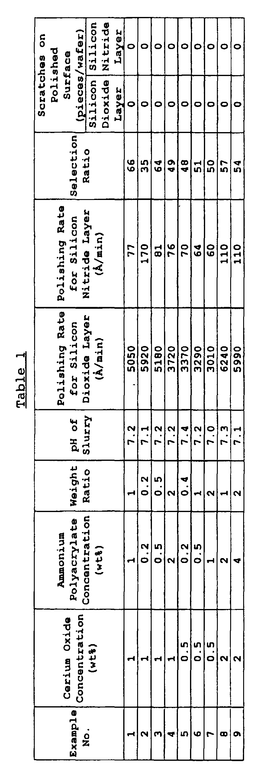
- polishing performance of this abrasive slurry for the silicon dioxide layer and for the silicon nitride layer was evaluated as follows.
- the polishing rate for the silicon dioxide layer was high and 5,050 ⁇ /min and the polishing rate for the silicon nitride layer was extremely low and 77 ⁇ /min. Accordingly, the selectivity ratio was as high as 66.
- a slurry of 10 wt% was prepared by diluting a silica slurry (SC-1, produced by Cabot KK, 30 wt%) and evaluated on the polishing performance. The results are shown in Table 3.
- a slurry of 1 wt% was prepared by diluting the same cerium oxide as used in Example 1. The water-soluble organic compound was not added. The polishing test was performed in the same manner as in Example 1 and the results are shown in Table 3.
- the abrasive composition for polishing a semiconductor device of the present invention is high in the polishing rate for silicon dioxide as the oxide layer, has a large selectivity ratio to the polishing rate for silicon nitride layer, and is reduced in scratches generated on the polished surface, hence, is suited as a composition for polishing a semiconductor device, used in polishing the oxide layer, in many cases, silicon dioxide layer, with a silicon nitride layer as the stopper.
Abstract
Description
wherein said planarization-polishing is performed by using an abrasive composition for polishing a semiconductor device, said composition mainly comprising water, cerium oxide powder and one or more water-soluble organic compound having at least one of a -COOH group, -COOMX group (wherein MX is an atom or functional group capable of replacing a H atom to form a salt), a -SO3H group or a -SO3MY group (wherein MY is an atom or functional group capable of replacing a H atom to form a salt).

- Material polished:
-
- (1) silicon dioxide layer (thickness: about 1 µm) formed on a silicon wafer having a diameter of 6" and a thickness of 625 µm by the CVD method
- (2) silicon nitride layer (thickness: about 0.5 µm) formed on a silicon wafer having a diameter of 6" and a thickness of 625 µm by the CVD method
- Pad:
- two layer-type pad for polishing a semiconductor device (IC1000/Suba400, manufactured by Rhodel-Nitta KK)
- Polishing machine:
- single side polishing machine for polishing a semiconductor device (Model SH-24, manufactured by Speedfam KK, work table diameter: 610 mm)
- Revolution number of table:
- 70 rpm
- Working pressure:
- 300 gf/cm2
- Slurry feeding rate:
- 100 ml/min
- Polishing time:
- 1 min
- Polishing rate:
- light interference-type layer thickness measuring apparatus
- Scratch:
- optical microscope dark-field observation (3% of the wafer surface was observed at 200 magnification and the number of scratches was converted into pieces/ wafer)


Claims (6)
- An abrasive composition for polishing a semiconductor device in the shallow trench isolation process, said composition mainly comprising water, cerium oxide powder and one or more water-soluble organic compound having at least one of a -COOH group, a -COOMX group (wherein MX is an atom or functional group capable of displacing a H atom to form a salt), a -SO3H group and a -SO3MY group (wherein MY represents an atom or functional group capable of displacing a H atom to form a salt).
- The abrasive composition for polishing a semiconductor device as claimed in claim 1, wherein the concentration of cerium oxide in the abrasive composition is from 0.1 to 10 wt% and the amount of the water-soluble organic compound added, in terms of the weight ratio to the cerium oxide, is from 0.001 to 20.
- The abrasive composition for polishing a semiconductor device as claimed in claim 1, wherein when a silicon nitride layer and a silicon oxide layer separately formed on a silicon substrate by the CVD method are independently polished under the same conditions, the ratio of the polishing rate for the former to that for the latter is 10 or more.
- A process for manufacturing a semiconductor device, comprising the steps offorming a silicon nitride layer on a semiconductor substrate,selectively removing a portion of said silicon nitride layer to expose said semiconductor substrate,ething said semiconductor substrate using said silicon nitride layer as a mask to form a trench,depositing a silicon oxide layer on said silicon nitride layer and said semiconductor substrate to completely fill said trench with the silicon oxide layer, andplanarization-polishing said silicon oxide layer using said silicon nitride layer as a stopper to selectively remain said silicon oxide in said trench,
wherein said planarization-polishing is performed by using an abrasive composition for polishing a semiconductor device, said composition mainly comprising water, cerium oxide powder and one or more water-soluble organic compound having at least one of a -COOH group, -COOMX group (wherein MX is an atom or functional group capable of replacing a H atom to form a salt), a -SO3H group or a -SO3MY group (wherein MY is an atom or functional group capable of replacing a H atom to form a salt). - The process for manufacturing a semiconductor device as set force in claim 4, wherein the concentration of cerium oxide in the abrasive composition is from 0.1 to 10 wt% and the amount of the water-soluble organic compound added, in terms of the weight ratio to the cerium oxide, is from 0.001 to 20.
- The process for manufacturing a semiconductor device as set forth in claim 4, wherein when a silicon nitride layer and a silicon oxide layer separately formed on a semiconductor substrate by the CVD method are independently polished under the same conditions, the ratio of the polishing rate for the former to that for the latter is 10 or more.
Applications Claiming Priority (3)
| Application Number | Priority Date | Filing Date | Title |
|---|---|---|---|
| JP4228898 | 1998-02-24 | ||
| JP4228898 | 1998-02-24 | ||
| PCT/JP1999/000844 WO1999043761A1 (en) | 1998-02-24 | 1999-02-24 | Abrasive composition for polishing semiconductor device and process for producing semiconductor device with the same |
Publications (3)
| Publication Number | Publication Date |
|---|---|
| EP1061111A1 true EP1061111A1 (en) | 2000-12-20 |
| EP1061111A4 EP1061111A4 (en) | 2001-05-30 |
| EP1061111B1 EP1061111B1 (en) | 2004-05-06 |
Family
ID=12631866
Family Applications (1)
| Application Number | Title | Priority Date | Filing Date |
|---|---|---|---|
| EP99906467A Expired - Lifetime EP1061111B1 (en) | 1998-02-24 | 1999-02-24 | Abrasive composition for polishing semiconductor device and process for producing semiconductor device with the same |
Country Status (9)
| Country | Link |
|---|---|
| US (2) | US6436835B1 (en) |
| EP (1) | EP1061111B1 (en) |
| JP (1) | JP3672493B2 (en) |
| KR (1) | KR100583842B1 (en) |
| AT (1) | ATE266071T1 (en) |
| DE (1) | DE69917010T2 (en) |
| ES (1) | ES2216490T3 (en) |
| TW (1) | TW510917B (en) |
| WO (1) | WO1999043761A1 (en) |
Cited By (11)
| Publication number | Priority date | Publication date | Assignee | Title |
|---|---|---|---|---|
| WO2003009349A2 (en) * | 2001-07-16 | 2003-01-30 | Applied Materials, Inc. | Methods and compositions for chemical mechanical polishing substrates covered with at least two dielectric materials |
| US6627107B2 (en) | 1999-12-08 | 2003-09-30 | Eastman Kodak Company | Slurry for chemical mechanical polishing silicon dioxide |
| US6677239B2 (en) | 2001-08-24 | 2004-01-13 | Applied Materials Inc. | Methods and compositions for chemical mechanical polishing |
| WO2004061925A1 (en) * | 2002-12-31 | 2004-07-22 | Sumitomo Mitsubishi Silicon Corporation | Slurry composition for chemical mechanical polishing, method for planarization of surface of semiconductor element using the same, and method for controlling selection ratio of slurry composition |
| WO2004069947A1 (en) * | 2003-02-03 | 2004-08-19 | Cabot Microelectronics Corporation | Method of polishing a silicon-containing dielectric |
| US7063597B2 (en) | 2002-10-25 | 2006-06-20 | Applied Materials | Polishing processes for shallow trench isolation substrates |
| US7199056B2 (en) | 2002-02-08 | 2007-04-03 | Applied Materials, Inc. | Low cost and low dishing slurry for polysilicon CMP |
| US7470295B2 (en) | 2004-03-12 | 2008-12-30 | K.C. Tech Co., Ltd. | Polishing slurry, method of producing same, and method of polishing substrate |
| US7677956B2 (en) | 2002-05-10 | 2010-03-16 | Cabot Microelectronics Corporation | Compositions and methods for dielectric CMP |
| WO2010139603A1 (en) | 2009-06-05 | 2010-12-09 | Basf Se | RASPBERRY-TYPE METAL OXIDE NANOSTRUCTURES COATED WITH CeO2 NANOPARTICLES FOR CHEMICAL MECHANICAL PLANARIZATION (CMP) |
| US10421890B2 (en) | 2016-03-31 | 2019-09-24 | Versum Materials Us, Llc | Composite particles, method of refining and use thereof |
Families Citing this family (59)
| Publication number | Priority date | Publication date | Assignee | Title |
|---|---|---|---|---|
| KR100366619B1 (en) * | 1999-05-12 | 2003-01-09 | 삼성전자 주식회사 | Trench isolation method, Method of manufacturing semiconductor device having trench and Semiconductor device formed thereby |
| JP2001055560A (en) * | 1999-08-18 | 2001-02-27 | Hitachi Chem Co Ltd | Polishing agent and method for polishing substrate by using the same |
| CN1125862C (en) * | 1999-09-20 | 2003-10-29 | 长兴化学工业股份有限公司 | Composite ground in chemical machine for semiconductor processing |
| JP2001144046A (en) * | 1999-11-12 | 2001-05-25 | Hitachi Chem Co Ltd | Metal polishing fluid and polishing method using it |
| US6491843B1 (en) * | 1999-12-08 | 2002-12-10 | Eastman Kodak Company | Slurry for chemical mechanical polishing silicon dioxide |
| TW586157B (en) * | 2000-04-13 | 2004-05-01 | Showa Denko Kk | Slurry composition for polishing semiconductor device, and method for manufacturing semiconductor device using the same |
| US6733553B2 (en) | 2000-04-13 | 2004-05-11 | Showa Denko Kabushiki Kaisha | Abrasive composition for polishing semiconductor device and method for producing semiconductor device using the same |
| US6607967B1 (en) * | 2000-11-15 | 2003-08-19 | Lsi Logic Corporation | Process for forming planarized isolation trench in integrated circuit structure on semiconductor substrate |
| JP5017574B2 (en) * | 2001-05-25 | 2012-09-05 | エア プロダクツ アンド ケミカルズ インコーポレイテッド | Cerium oxide abrasive and method for producing substrate |
| JP2003313542A (en) * | 2002-04-22 | 2003-11-06 | Jsr Corp | Aqueous dispersion for chemomechanical polishing use |
| KR100457743B1 (en) * | 2002-05-17 | 2004-11-18 | 주식회사 하이닉스반도체 | CMP Slurry for Oxide and Formation Method of Semiconductor Device Using the Same |
| CN100369211C (en) * | 2002-07-22 | 2008-02-13 | 清美化学股份有限公司 | Semiconductor polishing compound, process for its production and polishing method |
| KR20040042430A (en) * | 2002-11-14 | 2004-05-20 | 주식회사 하이닉스반도체 | Method for forming isolation layer of semiconductor device |
| KR100627510B1 (en) * | 2002-12-30 | 2006-09-22 | 주식회사 하이닉스반도체 | CMP slurry for nitride |
| US7066801B2 (en) * | 2003-02-21 | 2006-06-27 | Dow Global Technologies, Inc. | Method of manufacturing a fixed abrasive material |
| US6910951B2 (en) | 2003-02-24 | 2005-06-28 | Dow Global Technologies, Inc. | Materials and methods for chemical-mechanical planarization |
| KR100570122B1 (en) * | 2003-05-12 | 2006-04-11 | 학교법인 한양학원 | Slurry composition for chemical mechanical polishing capable of compensating nanotopography effect and method of planarizing surface of semiconductor device using the same |
| KR100539983B1 (en) * | 2003-05-15 | 2006-01-10 | 학교법인 한양학원 | Ceria Abrasives for CMP and Methods of Fabricating the Same |
| JP4637464B2 (en) * | 2003-07-01 | 2011-02-23 | Jsr株式会社 | Aqueous dispersion for chemical mechanical polishing |
| JP4574140B2 (en) * | 2003-08-27 | 2010-11-04 | 株式会社フジミインコーポレーテッド | Polishing composition and polishing method using the same |
| US6964600B2 (en) * | 2003-11-21 | 2005-11-15 | Praxair Technology, Inc. | High selectivity colloidal silica slurry |
| US20050108947A1 (en) * | 2003-11-26 | 2005-05-26 | Mueller Brian L. | Compositions and methods for chemical mechanical polishing silica and silicon nitride |
| US20050189322A1 (en) * | 2004-02-27 | 2005-09-01 | Lane Sarah J. | Compositions and methods for chemical mechanical polishing silica and silicon nitride |
| US20050211952A1 (en) * | 2004-03-29 | 2005-09-29 | Timothy Mace | Compositions and methods for chemical mechanical planarization of tungsten and titanium |
| US20050214191A1 (en) * | 2004-03-29 | 2005-09-29 | Mueller Brian L | Abrasives and compositions for chemical mechanical planarization of tungsten and titanium |
| TWI283008B (en) * | 2004-05-11 | 2007-06-21 | K C Tech Co Ltd | Slurry for CMP and method of producing the same |
| US20050279733A1 (en) * | 2004-06-18 | 2005-12-22 | Cabot Microelectronics Corporation | CMP composition for improved oxide removal rate |
| US20060021972A1 (en) * | 2004-07-28 | 2006-02-02 | Lane Sarah J | Compositions and methods for chemical mechanical polishing silicon dioxide and silicon nitride |
| TWI273632B (en) * | 2004-07-28 | 2007-02-11 | K C Tech Co Ltd | Polishing slurry, method of producing same, and method of polishing substrate |
| US7504044B2 (en) * | 2004-11-05 | 2009-03-17 | Cabot Microelectronics Corporation | Polishing composition and method for high silicon nitride to silicon oxide removal rate ratios |
| US7531105B2 (en) * | 2004-11-05 | 2009-05-12 | Cabot Microelectronics Corporation | Polishing composition and method for high silicon nitride to silicon oxide removal rate ratios |
| US20060097219A1 (en) * | 2004-11-08 | 2006-05-11 | Applied Materials, Inc. | High selectivity slurry compositions for chemical mechanical polishing |
| TWI323741B (en) * | 2004-12-16 | 2010-04-21 | K C Tech Co Ltd | Abrasive particles, polishing slurry, and producing method thereof |
| KR100641348B1 (en) * | 2005-06-03 | 2006-11-03 | 주식회사 케이씨텍 | Slurry for cmp and method of fabricating the same and method of polishing substrate |
| JP2007103514A (en) * | 2005-09-30 | 2007-04-19 | Fujimi Inc | Polishing composition and method therefor |
| CN101291778B (en) | 2005-10-19 | 2012-06-20 | 日立化成工业株式会社 | Cerium oxide slurry, cerium oxide polishing slurry and method for polishing substrate using the same |
| EP1994112B1 (en) * | 2006-01-25 | 2018-09-19 | LG Chem, Ltd. | Cmp slurry and method for polishing semiconductor wafer using the same |
| US20070210278A1 (en) * | 2006-03-08 | 2007-09-13 | Lane Sarah J | Compositions for chemical mechanical polishing silicon dioxide and silicon nitride |
| KR100814416B1 (en) * | 2006-09-28 | 2008-03-18 | 삼성전자주식회사 | High planarity slurry composition and method of chemical mechanical polishing using the same |
| JP2008117807A (en) * | 2006-10-31 | 2008-05-22 | Fujimi Inc | Polishing composition, and polishing method |
| JP2008130988A (en) * | 2006-11-24 | 2008-06-05 | Fujimi Inc | Polishing composition and polishing method |
| JP5375025B2 (en) * | 2008-02-27 | 2013-12-25 | 日立化成株式会社 | Polishing liquid |
| JP5819036B2 (en) * | 2008-03-25 | 2015-11-18 | 三井金属鉱業株式会社 | Cerium-based abrasive slurry |
| JP5104796B2 (en) * | 2009-03-30 | 2012-12-19 | 日立化成工業株式会社 | Abrasive and substrate polishing method using the same |
| CN102666760B (en) | 2009-11-11 | 2015-11-25 | 可乐丽股份有限公司 | Slurry for chemical mechanical polishing and use its finishing method of substrate |
| KR101675378B1 (en) | 2010-02-25 | 2016-11-23 | 삼성전자주식회사 | slurry for polishing and planarizion method of insulator layer used the same |
| MY164859A (en) | 2010-09-08 | 2018-01-30 | Basf Se | Aqueous polishing composition and process for chemically mechanically polishing substrate materials for electrical, mechanical and optical devices |
| CN103210047B (en) | 2010-09-08 | 2018-07-17 | 巴斯夫欧洲公司 | The diazene * dioxide of the substitution containing N and/or the aqueous polishing composition of N '-hydroxyls-diazene * oxide salts |
| KR101906135B1 (en) | 2010-09-08 | 2018-10-10 | 바스프 에스이 | Aqueous polishing composition and process for chemically mechanically polishing substrates containing silicon oxide dielectric and polysilicon films |
| JP6096670B2 (en) | 2010-12-10 | 2017-03-15 | ビーエーエスエフ ソシエタス・ヨーロピアBasf Se | Aqueous polishing composition and method for chemically and mechanically polishing a substrate containing a silicon oxide dielectric film and a polysilicon film |
| JP6001532B2 (en) | 2011-05-24 | 2016-10-05 | 株式会社クラレ | Chemical machine polishing erosion inhibitor, chemical mechanical polishing slurry and chemical mechanical polishing method |
| JP2013084836A (en) * | 2011-10-12 | 2013-05-09 | Toshiba Corp | Cmp method, and semiconductor device manufacturing method |
| US9777192B2 (en) * | 2012-02-10 | 2017-10-03 | Basf Se | Chemical mechanical polishing (CMP) composition comprising a protein |
| EP2858097B1 (en) | 2012-05-30 | 2019-02-27 | Kuraray Co., Ltd. | Slurry for chemical mechanical polishing and chemical mechanical polishing method |
| US9583359B2 (en) | 2014-04-04 | 2017-02-28 | Fujifilm Planar Solutions, LLC | Polishing compositions and methods for selectively polishing silicon nitride over silicon oxide films |
| JP5893700B1 (en) * | 2014-09-26 | 2016-03-23 | 花王株式会社 | Polishing liquid composition for silicon oxide film |
| WO2016158648A1 (en) * | 2015-03-30 | 2016-10-06 | Jsr株式会社 | Processing composition for polishing chemical machinery, and chemical machinery polishing method and washing method |
| JP6582567B2 (en) * | 2015-06-03 | 2019-10-02 | 日立化成株式会社 | Slurry and manufacturing method thereof, and polishing method |
| US20230420260A1 (en) * | 2020-11-27 | 2023-12-28 | Kao Corporation | Polishing liquid composition for silicon oxide film |
Citations (2)
| Publication number | Priority date | Publication date | Assignee | Title |
|---|---|---|---|---|
| EP0786504A2 (en) * | 1996-01-29 | 1997-07-30 | Fujimi Incorporated | Polishing composition |
| EP1043379A1 (en) * | 1997-12-18 | 2000-10-11 | Hitachi Chemical Company, Ltd. | Abrasive, method of polishing wafer, and method of producing semiconductor device |
Family Cites Families (9)
| Publication number | Priority date | Publication date | Assignee | Title |
|---|---|---|---|---|
| JPH0841443A (en) | 1994-07-26 | 1996-02-13 | Okuno Chem Ind Co Ltd | Polishing composition and polishing method |
| JPH08302338A (en) | 1995-05-15 | 1996-11-19 | Sony Corp | Slurry and production of semiconductor device by using same |
| JP3230986B2 (en) * | 1995-11-13 | 2001-11-19 | 株式会社東芝 | Polishing method, semiconductor device manufacturing method, and semiconductor manufacturing apparatus. |
| JP3514908B2 (en) | 1995-11-13 | 2004-04-05 | 株式会社東芝 | Abrasive |
| JPH09137156A (en) | 1995-11-16 | 1997-05-27 | Mitsubishi Chem Corp | Polishing composition for hard disk substrate and polishing method therewith |
| JPH09208933A (en) | 1996-01-29 | 1997-08-12 | Fujimi Inkooporeetetsudo:Kk | Composition for polishing |
| US5738800A (en) | 1996-09-27 | 1998-04-14 | Rodel, Inc. | Composition and method for polishing a composite of silica and silicon nitride |
| JPH10321570A (en) * | 1997-05-15 | 1998-12-04 | Tokuyama Corp | Abrasive for polishing semiconductor wafer, its manufacture, and polishing method |
| JPH10279928A (en) | 1998-02-27 | 1998-10-20 | Rodel Inc | Compound for controlling polishing speed |
-
1999
- 1999-02-24 WO PCT/JP1999/000844 patent/WO1999043761A1/en active IP Right Grant
- 1999-02-24 DE DE69917010T patent/DE69917010T2/en not_active Expired - Lifetime
- 1999-02-24 US US09/622,939 patent/US6436835B1/en not_active Expired - Lifetime
- 1999-02-24 AT AT99906467T patent/ATE266071T1/en active
- 1999-02-24 ES ES99906467T patent/ES2216490T3/en not_active Expired - Lifetime
- 1999-02-24 TW TW088102755A patent/TW510917B/en not_active IP Right Cessation
- 1999-02-24 KR KR1020007009341A patent/KR100583842B1/en not_active IP Right Cessation
- 1999-02-24 JP JP2000533504A patent/JP3672493B2/en not_active Expired - Lifetime
- 1999-02-24 EP EP99906467A patent/EP1061111B1/en not_active Expired - Lifetime
-
2001
- 2001-09-17 US US09/953,127 patent/US6410444B1/en not_active Expired - Lifetime
Patent Citations (2)
| Publication number | Priority date | Publication date | Assignee | Title |
|---|---|---|---|---|
| EP0786504A2 (en) * | 1996-01-29 | 1997-07-30 | Fujimi Incorporated | Polishing composition |
| EP1043379A1 (en) * | 1997-12-18 | 2000-10-11 | Hitachi Chemical Company, Ltd. | Abrasive, method of polishing wafer, and method of producing semiconductor device |
Non-Patent Citations (3)
| Title |
|---|
| READE ADVANCED MATERIALS, [Online] XP002164382 Retrieved from the Internet: <URL:http://www.reade.com/Products/Mineral s_and_Ores/quartz.html> [retrieved on 2001-03-30] * |
| See also references of WO9943761A1 * |
| UNIVERSITY OF LINCOLNSHIRE & HUMBERSIDE, [Online] XP002164381 Retrieved from the Internet: <URL:http://seit.humber.ac.uk/~tharris/EGF 539/Lectures/silicon_nitride.htm> [retrieved on 2001-03-30] * |
Cited By (19)
| Publication number | Priority date | Publication date | Assignee | Title |
|---|---|---|---|---|
| US6627107B2 (en) | 1999-12-08 | 2003-09-30 | Eastman Kodak Company | Slurry for chemical mechanical polishing silicon dioxide |
| US7091164B2 (en) | 1999-12-08 | 2006-08-15 | Eastman Kodak Company | Slurry for chemical mechanical polishing silicon dioxide |
| WO2003009349A3 (en) * | 2001-07-16 | 2003-10-16 | Applied Materials Inc | Methods and compositions for chemical mechanical polishing substrates covered with at least two dielectric materials |
| US6811470B2 (en) | 2001-07-16 | 2004-11-02 | Applied Materials Inc. | Methods and compositions for chemical mechanical polishing shallow trench isolation substrates |
| WO2003009349A2 (en) * | 2001-07-16 | 2003-01-30 | Applied Materials, Inc. | Methods and compositions for chemical mechanical polishing substrates covered with at least two dielectric materials |
| US6677239B2 (en) | 2001-08-24 | 2004-01-13 | Applied Materials Inc. | Methods and compositions for chemical mechanical polishing |
| US7199056B2 (en) | 2002-02-08 | 2007-04-03 | Applied Materials, Inc. | Low cost and low dishing slurry for polysilicon CMP |
| US7677956B2 (en) | 2002-05-10 | 2010-03-16 | Cabot Microelectronics Corporation | Compositions and methods for dielectric CMP |
| US7063597B2 (en) | 2002-10-25 | 2006-06-20 | Applied Materials | Polishing processes for shallow trench isolation substrates |
| WO2004061925A1 (en) * | 2002-12-31 | 2004-07-22 | Sumitomo Mitsubishi Silicon Corporation | Slurry composition for chemical mechanical polishing, method for planarization of surface of semiconductor element using the same, and method for controlling selection ratio of slurry composition |
| CN1748292B (en) * | 2002-12-31 | 2010-09-01 | 三菱住友硅晶株式会社 | Slurry composition for chemical mechanical polishing, method for planarization of surface of semiconductor element using the same, and method for controlling selection ratio of slurry composition |
| US7071105B2 (en) | 2003-02-03 | 2006-07-04 | Cabot Microelectronics Corporation | Method of polishing a silicon-containing dielectric |
| US7442645B2 (en) | 2003-02-03 | 2008-10-28 | Cabot Microelectronics Corporation | Method of polishing a silicon-containing dielectric |
| WO2004069947A1 (en) * | 2003-02-03 | 2004-08-19 | Cabot Microelectronics Corporation | Method of polishing a silicon-containing dielectric |
| US8486169B2 (en) | 2003-02-03 | 2013-07-16 | Cabot Microelectronics Corporation | Method of polishing a silicon-containing dielectric |
| CN1742066B (en) * | 2003-02-03 | 2015-10-21 | 卡伯特微电子公司 | The siliceous dielectric method of polishing |
| US7470295B2 (en) | 2004-03-12 | 2008-12-30 | K.C. Tech Co., Ltd. | Polishing slurry, method of producing same, and method of polishing substrate |
| WO2010139603A1 (en) | 2009-06-05 | 2010-12-09 | Basf Se | RASPBERRY-TYPE METAL OXIDE NANOSTRUCTURES COATED WITH CeO2 NANOPARTICLES FOR CHEMICAL MECHANICAL PLANARIZATION (CMP) |
| US10421890B2 (en) | 2016-03-31 | 2019-09-24 | Versum Materials Us, Llc | Composite particles, method of refining and use thereof |
Also Published As
| Publication number | Publication date |
|---|---|
| US6410444B1 (en) | 2002-06-25 |
| TW510917B (en) | 2002-11-21 |
| EP1061111A4 (en) | 2001-05-30 |
| US6436835B1 (en) | 2002-08-20 |
| ATE266071T1 (en) | 2004-05-15 |
| JP3672493B2 (en) | 2005-07-20 |
| DE69917010T2 (en) | 2005-04-07 |
| US20020045350A1 (en) | 2002-04-18 |
| EP1061111B1 (en) | 2004-05-06 |
| KR100583842B1 (en) | 2006-05-26 |
| KR20010041248A (en) | 2001-05-15 |
| WO1999043761A1 (en) | 1999-09-02 |
| DE69917010D1 (en) | 2004-06-09 |
| ES2216490T3 (en) | 2004-10-16 |
Similar Documents
| Publication | Publication Date | Title |
|---|---|---|
| EP1061111B1 (en) | Abrasive composition for polishing semiconductor device and process for producing semiconductor device with the same | |
| CN101767295B (en) | Chemical mechanical polishing composition and methods relating thereto | |
| US6019806A (en) | High selectivity slurry for shallow trench isolation processing | |
| US20080283502A1 (en) | Compositions, methods and systems for polishing aluminum oxide and aluminum oxynitride substrates | |
| JP2001200242A (en) | Aqueous slurry | |
| KR20080039279A (en) | Polishing composition and polishing process | |
| JP5363338B2 (en) | Chemical mechanical planarization composition, system, and method of use | |
| EP0853335A2 (en) | Slurry and process for the mechano-chemical polishing of semiconductor devices | |
| KR100863088B1 (en) | Polishing compound for polishing semiconductor device and method for manufacturing semiconductor device using the same | |
| TW202039776A (en) | Chemical mechanical polishing compositons and methods for suppressing the removal rate of amorphous silicon | |
| US20100243471A1 (en) | Composition, method and process for polishing a wafer | |
| WO2006071475A2 (en) | Wafer planarization composition and method of use | |
| EP0853110B1 (en) | CMP slurry with high selectivity | |
| KR100684877B1 (en) | Slurry compositions and favrication method of semiconductor device including chemical mechanical polishing process using the same | |
| KR20200132755A (en) | Chemical Mechanical Polishing Composition And Method Of Polishing Silicon Nitride Over Silicon Dioxide And Simultaneously Inhibiting Damage To Silicon Dioxide | |
| KR20200132756A (en) | Chemical mechanical polishing compositions and methods having enhanced defect inhibition and selectively polishing silicon nitride over silicon dioxide in an acid environment | |
| KR100464748B1 (en) | Composition and Method for Polishing a Composite | |
| KR100466422B1 (en) | Composition for chemical mechanical polishing | |
| CN110964440A (en) | Chemical mechanical polishing composition and method for polishing silicon dioxide over silicon nitride |
Legal Events
| Date | Code | Title | Description |
|---|---|---|---|
| PUAI | Public reference made under article 153(3) epc to a published international application that has entered the european phase |
Free format text: ORIGINAL CODE: 0009012 |
|
| 17P | Request for examination filed |
Effective date: 20000914 |
|
| AK | Designated contracting states |
Kind code of ref document: A1 Designated state(s): AT BE CH CY DE DK ES FI FR GB GR IE IT LI LU MC NL PT SE |
|
| A4 | Supplementary search report drawn up and despatched |
Effective date: 20010412 |
|
| AK | Designated contracting states |
Kind code of ref document: A4 Designated state(s): AT BE CH CY DE DK ES FI FR GB GR IE IT LI LU MC NL PT SE |
|
| 17Q | First examination report despatched |
Effective date: 20020422 |
|
| GRAP | Despatch of communication of intention to grant a patent |
Free format text: ORIGINAL CODE: EPIDOSNIGR1 |
|
| GRAS | Grant fee paid |
Free format text: ORIGINAL CODE: EPIDOSNIGR3 |
|
| GRAA | (expected) grant |
Free format text: ORIGINAL CODE: 0009210 |
|
| AK | Designated contracting states |
Kind code of ref document: B1 Designated state(s): AT BE CH CY DE DK ES FI FR GB GR IE IT LI LU MC NL PT SE |
|
| PG25 | Lapsed in a contracting state [announced via postgrant information from national office to epo] |
Ref country code: FI Free format text: LAPSE BECAUSE OF FAILURE TO SUBMIT A TRANSLATION OF THE DESCRIPTION OR TO PAY THE FEE WITHIN THE PRESCRIBED TIME-LIMIT Effective date: 20040506 |
|
| REG | Reference to a national code |
Ref country code: GB Ref legal event code: FG4D |
|
| REG | Reference to a national code |
Ref country code: CH Ref legal event code: EP |
|
| REF | Corresponds to: |
Ref document number: 69917010 Country of ref document: DE Date of ref document: 20040609 Kind code of ref document: P |
|
| REG | Reference to a national code |
Ref country code: IE Ref legal event code: FG4D |
|
| REG | Reference to a national code |
Ref country code: CH Ref legal event code: NV Representative=s name: PATENTANWAELTE SCHAAD, BALASS, MENZL & PARTNER AG |
|
| PG25 | Lapsed in a contracting state [announced via postgrant information from national office to epo] |
Ref country code: SE Free format text: LAPSE BECAUSE OF FAILURE TO SUBMIT A TRANSLATION OF THE DESCRIPTION OR TO PAY THE FEE WITHIN THE PRESCRIBED TIME-LIMIT Effective date: 20040806 Ref country code: GR Free format text: LAPSE BECAUSE OF FAILURE TO SUBMIT A TRANSLATION OF THE DESCRIPTION OR TO PAY THE FEE WITHIN THE PRESCRIBED TIME-LIMIT Effective date: 20040806 Ref country code: DK Free format text: LAPSE BECAUSE OF FAILURE TO SUBMIT A TRANSLATION OF THE DESCRIPTION OR TO PAY THE FEE WITHIN THE PRESCRIBED TIME-LIMIT Effective date: 20040806 |
|
| REG | Reference to a national code |
Ref country code: ES Ref legal event code: FG2A Ref document number: 2216490 Country of ref document: ES Kind code of ref document: T3 |
|
| ET | Fr: translation filed | ||
| PG25 | Lapsed in a contracting state [announced via postgrant information from national office to epo] |
Ref country code: LU Free format text: LAPSE BECAUSE OF NON-PAYMENT OF DUE FEES Effective date: 20050224 Ref country code: CY Free format text: LAPSE BECAUSE OF FAILURE TO SUBMIT A TRANSLATION OF THE DESCRIPTION OR TO PAY THE FEE WITHIN THE PRESCRIBED TIME-LIMIT Effective date: 20050224 |
|
| PG25 | Lapsed in a contracting state [announced via postgrant information from national office to epo] |
Ref country code: MC Free format text: LAPSE BECAUSE OF NON-PAYMENT OF DUE FEES Effective date: 20050228 |
|
| PLBE | No opposition filed within time limit |
Free format text: ORIGINAL CODE: 0009261 |
|
| STAA | Information on the status of an ep patent application or granted ep patent |
Free format text: STATUS: NO OPPOSITION FILED WITHIN TIME LIMIT |
|
| 26N | No opposition filed |
Effective date: 20050208 |
|
| PG25 | Lapsed in a contracting state [announced via postgrant information from national office to epo] |
Ref country code: PT Free format text: LAPSE BECAUSE OF NON-PAYMENT OF DUE FEES Effective date: 20041006 |
|
| PGFP | Annual fee paid to national office [announced via postgrant information from national office to epo] |
Ref country code: IE Payment date: 20110217 Year of fee payment: 13 |
|
| PGFP | Annual fee paid to national office [announced via postgrant information from national office to epo] |
Ref country code: NL Payment date: 20110304 Year of fee payment: 13 |
|
| PGFP | Annual fee paid to national office [announced via postgrant information from national office to epo] |
Ref country code: ES Payment date: 20110218 Year of fee payment: 13 Ref country code: GB Payment date: 20110223 Year of fee payment: 13 |
|
| REG | Reference to a national code |
Ref country code: NL Ref legal event code: V1 Effective date: 20120901 |
|
| GBPC | Gb: european patent ceased through non-payment of renewal fee |
Effective date: 20120224 |
|
| REG | Reference to a national code |
Ref country code: IE Ref legal event code: MM4A |
|
| PG25 | Lapsed in a contracting state [announced via postgrant information from national office to epo] |
Ref country code: IE Free format text: LAPSE BECAUSE OF NON-PAYMENT OF DUE FEES Effective date: 20120224 Ref country code: NL Free format text: LAPSE BECAUSE OF NON-PAYMENT OF DUE FEES Effective date: 20120901 Ref country code: GB Free format text: LAPSE BECAUSE OF NON-PAYMENT OF DUE FEES Effective date: 20120224 |
|
| REG | Reference to a national code |
Ref country code: ES Ref legal event code: FD2A Effective date: 20130709 |
|
| PG25 | Lapsed in a contracting state [announced via postgrant information from national office to epo] |
Ref country code: ES Free format text: LAPSE BECAUSE OF NON-PAYMENT OF DUE FEES Effective date: 20120225 |
|
| PGFP | Annual fee paid to national office [announced via postgrant information from national office to epo] |
Ref country code: CH Payment date: 20140212 Year of fee payment: 16 |
|
| PGFP | Annual fee paid to national office [announced via postgrant information from national office to epo] |
Ref country code: BE Payment date: 20140214 Year of fee payment: 16 Ref country code: AT Payment date: 20140128 Year of fee payment: 16 |
|
| REG | Reference to a national code |
Ref country code: CH Ref legal event code: PUE Owner name: HITACHI CHEMICAL COMPANY, LTD., JP Free format text: FORMER OWNER: SHOWA DENKO KABUSHIKI KAISHA, JP |
|
| REG | Reference to a national code |
Ref country code: DE Ref legal event code: R082 Ref document number: 69917010 Country of ref document: DE Representative=s name: PATENTANWAELTE STREHL, SCHUEBEL-HOPF & PARTNER, DE |
|
| REG | Reference to a national code |
Ref country code: AT Ref legal event code: PC Ref document number: 266071 Country of ref document: AT Kind code of ref document: T Owner name: HITACHI CHEMICAL COMPANY, LTD., JP Effective date: 20141107 |
|
| REG | Reference to a national code |
Ref country code: DE Ref legal event code: R082 Ref document number: 69917010 Country of ref document: DE Representative=s name: STREHL SCHUEBEL-HOPF & PARTNER MBB PATENTANWAE, DE Effective date: 20141121 Ref country code: DE Ref legal event code: R082 Ref document number: 69917010 Country of ref document: DE Representative=s name: PATENTANWAELTE STREHL, SCHUEBEL-HOPF & PARTNER, DE Effective date: 20141121 Ref country code: DE Ref legal event code: R081 Ref document number: 69917010 Country of ref document: DE Owner name: HITACHI CHEMICAL COMPANY LTD., JP Free format text: FORMER OWNER: SHOWA DENKO K.K., TOKIO/TOKYO, JP Effective date: 20141121 |
|
| REG | Reference to a national code |
Ref country code: FR Ref legal event code: TP Owner name: HITACHI CHEMICAL COMPANY, LTD., JP Effective date: 20141128 |
|
| PG25 | Lapsed in a contracting state [announced via postgrant information from national office to epo] |
Ref country code: BE Free format text: LAPSE BECAUSE OF NON-PAYMENT OF DUE FEES Effective date: 20150228 |
|
| REG | Reference to a national code |
Ref country code: CH Ref legal event code: PL |
|
| REG | Reference to a national code |
Ref country code: AT Ref legal event code: MM01 Ref document number: 266071 Country of ref document: AT Kind code of ref document: T Effective date: 20150224 |
|
| PG25 | Lapsed in a contracting state [announced via postgrant information from national office to epo] |
Ref country code: LI Free format text: LAPSE BECAUSE OF NON-PAYMENT OF DUE FEES Effective date: 20150228 Ref country code: CH Free format text: LAPSE BECAUSE OF NON-PAYMENT OF DUE FEES Effective date: 20150228 |
|
| PG25 | Lapsed in a contracting state [announced via postgrant information from national office to epo] |
Ref country code: AT Free format text: LAPSE BECAUSE OF NON-PAYMENT OF DUE FEES Effective date: 20150224 |
|
| REG | Reference to a national code |
Ref country code: FR Ref legal event code: PLFP Year of fee payment: 18 |
|
| REG | Reference to a national code |
Ref country code: FR Ref legal event code: PLFP Year of fee payment: 19 |
|
| REG | Reference to a national code |
Ref country code: FR Ref legal event code: PLFP Year of fee payment: 20 |
|
| PGFP | Annual fee paid to national office [announced via postgrant information from national office to epo] |
Ref country code: DE Payment date: 20180214 Year of fee payment: 20 |
|
| PGFP | Annual fee paid to national office [announced via postgrant information from national office to epo] |
Ref country code: IT Payment date: 20180221 Year of fee payment: 20 Ref country code: FR Payment date: 20180111 Year of fee payment: 20 |
|
| REG | Reference to a national code |
Ref country code: DE Ref legal event code: R071 Ref document number: 69917010 Country of ref document: DE |