EP1059663A2 - Process for producing a semiconductor thin film with a bonding and separating steps, solar cell fabrication and anodizing apparatus - Google Patents
Process for producing a semiconductor thin film with a bonding and separating steps, solar cell fabrication and anodizing apparatus Download PDFInfo
- Publication number
- EP1059663A2 EP1059663A2 EP00112239A EP00112239A EP1059663A2 EP 1059663 A2 EP1059663 A2 EP 1059663A2 EP 00112239 A EP00112239 A EP 00112239A EP 00112239 A EP00112239 A EP 00112239A EP 1059663 A2 EP1059663 A2 EP 1059663A2
- Authority
- EP
- European Patent Office
- Prior art keywords
- substrate
- layer
- semiconductor layer
- producing
- semiconductor
- Prior art date
- Legal status (The legal status is an assumption and is not a legal conclusion. Google has not performed a legal analysis and makes no representation as to the accuracy of the status listed.)
- Withdrawn
Links
- 239000004065 semiconductor Substances 0.000 title claims abstract description 251
- 238000000034 method Methods 0.000 title claims abstract description 102
- 238000007743 anodising Methods 0.000 title claims abstract description 100
- 239000010409 thin film Substances 0.000 title claims abstract description 81
- 238000004519 manufacturing process Methods 0.000 title abstract description 19
- 239000000758 substrate Substances 0.000 claims abstract description 295
- 239000013078 crystal Substances 0.000 claims abstract description 57
- 230000002093 peripheral effect Effects 0.000 claims abstract description 47
- 238000000926 separation method Methods 0.000 claims abstract description 36
- 229910052710 silicon Inorganic materials 0.000 claims description 179
- 239000010703 silicon Substances 0.000 claims description 179
- 239000010408 film Substances 0.000 claims description 40
- 238000005530 etching Methods 0.000 claims description 28
- 238000005468 ion implantation Methods 0.000 claims description 6
- BASFCYQUMIYNBI-UHFFFAOYSA-N platinum Chemical compound [Pt] BASFCYQUMIYNBI-UHFFFAOYSA-N 0.000 claims description 4
- 229910052697 platinum Inorganic materials 0.000 claims description 2
- 230000007547 defect Effects 0.000 abstract description 6
- 239000010410 layer Substances 0.000 description 577
- XUIMIQQOPSSXEZ-UHFFFAOYSA-N Silicon Chemical compound [Si] XUIMIQQOPSSXEZ-UHFFFAOYSA-N 0.000 description 175
- 235000012431 wafers Nutrition 0.000 description 122
- KRHYYFGTRYWZRS-UHFFFAOYSA-N Fluorane Chemical compound F KRHYYFGTRYWZRS-UHFFFAOYSA-N 0.000 description 87
- 229910021421 monocrystalline silicon Inorganic materials 0.000 description 64
- 239000000243 solution Substances 0.000 description 50
- 229910000040 hydrogen fluoride Inorganic materials 0.000 description 48
- 229910021426 porous silicon Inorganic materials 0.000 description 27
- LFQSCWFLJHTTHZ-UHFFFAOYSA-N Ethanol Chemical compound CCO LFQSCWFLJHTTHZ-UHFFFAOYSA-N 0.000 description 26
- 239000002344 surface layer Substances 0.000 description 22
- 229920001721 polyimide Polymers 0.000 description 15
- 235000019441 ethanol Nutrition 0.000 description 14
- 239000011521 glass Substances 0.000 description 14
- 239000000853 adhesive Substances 0.000 description 13
- 230000001070 adhesive effect Effects 0.000 description 13
- 238000009792 diffusion process Methods 0.000 description 13
- HEMHJVSKTPXQMS-UHFFFAOYSA-M Sodium hydroxide Chemical compound [OH-].[Na+] HEMHJVSKTPXQMS-UHFFFAOYSA-M 0.000 description 12
- 230000000694 effects Effects 0.000 description 12
- 238000002230 thermal chemical vapour deposition Methods 0.000 description 12
- 238000004943 liquid phase epitaxy Methods 0.000 description 11
- ZOXJGFHDIHLPTG-UHFFFAOYSA-N Boron Chemical compound [B] ZOXJGFHDIHLPTG-UHFFFAOYSA-N 0.000 description 10
- KWYUFKZDYYNOTN-UHFFFAOYSA-M Potassium hydroxide Chemical compound [OH-].[K+] KWYUFKZDYYNOTN-UHFFFAOYSA-M 0.000 description 10
- 229910052796 boron Inorganic materials 0.000 description 10
- 239000007789 gas Substances 0.000 description 10
- 239000000463 material Substances 0.000 description 9
- 229910021424 microcrystalline silicon Inorganic materials 0.000 description 9
- 239000002904 solvent Substances 0.000 description 9
- OAKJQQAXSVQMHS-UHFFFAOYSA-N Hydrazine Chemical compound NN OAKJQQAXSVQMHS-UHFFFAOYSA-N 0.000 description 8
- BQCADISMDOOEFD-UHFFFAOYSA-N Silver Chemical compound [Ag] BQCADISMDOOEFD-UHFFFAOYSA-N 0.000 description 8
- 229920006355 Tefzel Polymers 0.000 description 8
- 229910052782 aluminium Inorganic materials 0.000 description 8
- XAGFODPZIPBFFR-UHFFFAOYSA-N aluminium Chemical compound [Al] XAGFODPZIPBFFR-UHFFFAOYSA-N 0.000 description 8
- QHSJIZLJUFMIFP-UHFFFAOYSA-N ethene;1,1,2,2-tetrafluoroethene Chemical compound C=C.FC(F)=C(F)F QHSJIZLJUFMIFP-UHFFFAOYSA-N 0.000 description 8
- 238000002955 isolation Methods 0.000 description 8
- 238000005268 plasma chemical vapour deposition Methods 0.000 description 8
- 229910052709 silver Inorganic materials 0.000 description 8
- 239000004332 silver Substances 0.000 description 8
- 230000015572 biosynthetic process Effects 0.000 description 7
- 238000006243 chemical reaction Methods 0.000 description 7
- 238000005229 chemical vapour deposition Methods 0.000 description 7
- 238000010276 construction Methods 0.000 description 7
- 229910021420 polycrystalline silicon Inorganic materials 0.000 description 7
- QOSATHPSBFQAML-UHFFFAOYSA-N hydrogen peroxide;hydrate Chemical compound O.OO QOSATHPSBFQAML-UHFFFAOYSA-N 0.000 description 6
- 229910052738 indium Inorganic materials 0.000 description 6
- 239000011259 mixed solution Substances 0.000 description 6
- BLRPTPMANUNPDV-UHFFFAOYSA-N Silane Chemical compound [SiH4] BLRPTPMANUNPDV-UHFFFAOYSA-N 0.000 description 5
- 239000002019 doping agent Substances 0.000 description 5
- 239000001257 hydrogen Substances 0.000 description 5
- 229910052739 hydrogen Inorganic materials 0.000 description 5
- 239000000203 mixture Substances 0.000 description 5
- 239000010935 stainless steel Substances 0.000 description 5
- 229910001220 stainless steel Inorganic materials 0.000 description 5
- 238000003756 stirring Methods 0.000 description 5
- 238000001771 vacuum deposition Methods 0.000 description 5
- 229910015844 BCl3 Inorganic materials 0.000 description 4
- 238000010894 electron beam technology Methods 0.000 description 4
- 239000012535 impurity Substances 0.000 description 4
- APFVFJFRJDLVQX-UHFFFAOYSA-N indium atom Chemical compound [In] APFVFJFRJDLVQX-UHFFFAOYSA-N 0.000 description 4
- 229910052751 metal Inorganic materials 0.000 description 4
- 239000002184 metal Substances 0.000 description 4
- FAQYAMRNWDIXMY-UHFFFAOYSA-N trichloroborane Chemical compound ClB(Cl)Cl FAQYAMRNWDIXMY-UHFFFAOYSA-N 0.000 description 4
- XLYOFNOQVPJJNP-UHFFFAOYSA-N water Substances O XLYOFNOQVPJJNP-UHFFFAOYSA-N 0.000 description 4
- VEXZGXHMUGYJMC-UHFFFAOYSA-N Hydrochloric acid Chemical compound Cl VEXZGXHMUGYJMC-UHFFFAOYSA-N 0.000 description 3
- UFHFLCQGNIYNRP-UHFFFAOYSA-N Hydrogen Chemical compound [H][H] UFHFLCQGNIYNRP-UHFFFAOYSA-N 0.000 description 3
- GRYLNZFGIOXLOG-UHFFFAOYSA-N Nitric acid Chemical compound O[N+]([O-])=O GRYLNZFGIOXLOG-UHFFFAOYSA-N 0.000 description 3
- VYPSYNLAJGMNEJ-UHFFFAOYSA-N Silicium dioxide Chemical compound O=[Si]=O VYPSYNLAJGMNEJ-UHFFFAOYSA-N 0.000 description 3
- 239000003513 alkali Substances 0.000 description 3
- 238000010438 heat treatment Methods 0.000 description 3
- 150000002500 ions Chemical class 0.000 description 3
- 239000007791 liquid phase Substances 0.000 description 3
- 238000004518 low pressure chemical vapour deposition Methods 0.000 description 3
- 229910017604 nitric acid Inorganic materials 0.000 description 3
- 238000001020 plasma etching Methods 0.000 description 3
- 238000005498 polishing Methods 0.000 description 3
- 239000000047 product Substances 0.000 description 3
- 238000007650 screen-printing Methods 0.000 description 3
- 238000003631 wet chemical etching Methods 0.000 description 3
- IJGRMHOSHXDMSA-UHFFFAOYSA-N Atomic nitrogen Chemical compound N#N IJGRMHOSHXDMSA-UHFFFAOYSA-N 0.000 description 2
- RYGMFSIKBFXOCR-UHFFFAOYSA-N Copper Chemical compound [Cu] RYGMFSIKBFXOCR-UHFFFAOYSA-N 0.000 description 2
- OAICVXFJPJFONN-UHFFFAOYSA-N Phosphorus Chemical compound [P] OAICVXFJPJFONN-UHFFFAOYSA-N 0.000 description 2
- QAOWNCQODCNURD-UHFFFAOYSA-N Sulfuric acid Chemical compound OS(O)(=O)=O QAOWNCQODCNURD-UHFFFAOYSA-N 0.000 description 2
- GWEVSGVZZGPLCZ-UHFFFAOYSA-N Titan oxide Chemical compound O=[Ti]=O GWEVSGVZZGPLCZ-UHFFFAOYSA-N 0.000 description 2
- 239000002253 acid Substances 0.000 description 2
- 150000007513 acids Chemical class 0.000 description 2
- 238000000137 annealing Methods 0.000 description 2
- 239000012298 atmosphere Substances 0.000 description 2
- 230000005540 biological transmission Effects 0.000 description 2
- DQXBYHZEEUGOBF-UHFFFAOYSA-N but-3-enoic acid;ethene Chemical compound C=C.OC(=O)CC=C DQXBYHZEEUGOBF-UHFFFAOYSA-N 0.000 description 2
- 239000012295 chemical reaction liquid Substances 0.000 description 2
- 239000007795 chemical reaction product Substances 0.000 description 2
- 239000003795 chemical substances by application Substances 0.000 description 2
- 238000001816 cooling Methods 0.000 description 2
- 229910052802 copper Inorganic materials 0.000 description 2
- 239000010949 copper Substances 0.000 description 2
- 238000000407 epitaxy Methods 0.000 description 2
- 239000005038 ethylene vinyl acetate Substances 0.000 description 2
- 238000000227 grinding Methods 0.000 description 2
- 150000002431 hydrogen Chemical class 0.000 description 2
- 230000000873 masking effect Effects 0.000 description 2
- 239000012071 phase Substances 0.000 description 2
- 229910052698 phosphorus Inorganic materials 0.000 description 2
- 239000011574 phosphorus Substances 0.000 description 2
- 238000000053 physical method Methods 0.000 description 2
- 239000004033 plastic Substances 0.000 description 2
- 229920003023 plastic Polymers 0.000 description 2
- 229920001200 poly(ethylene-vinyl acetate) Polymers 0.000 description 2
- 239000011148 porous material Substances 0.000 description 2
- 229920005989 resin Polymers 0.000 description 2
- 239000011347 resin Substances 0.000 description 2
- 150000004756 silanes Chemical class 0.000 description 2
- 238000010583 slow cooling Methods 0.000 description 2
- 238000004544 sputter deposition Methods 0.000 description 2
- 229910052718 tin Inorganic materials 0.000 description 2
- 239000004593 Epoxy Substances 0.000 description 1
- 229910007260 Si2F6 Inorganic materials 0.000 description 1
- 229910007264 Si2H6 Inorganic materials 0.000 description 1
- 229910003910 SiCl4 Inorganic materials 0.000 description 1
- -1 SiH2Cl2 Chemical class 0.000 description 1
- 229910003818 SiH2Cl2 Inorganic materials 0.000 description 1
- 229910003816 SiH2F2 Inorganic materials 0.000 description 1
- 229910003822 SiHCl3 Inorganic materials 0.000 description 1
- 239000004809 Teflon Substances 0.000 description 1
- 229920006362 Teflon® Polymers 0.000 description 1
- 239000012790 adhesive layer Substances 0.000 description 1
- 230000002411 adverse Effects 0.000 description 1
- 150000001298 alcohols Chemical class 0.000 description 1
- 229910045601 alloy Inorganic materials 0.000 description 1
- 239000000956 alloy Substances 0.000 description 1
- CSDREXVUYHZDNP-UHFFFAOYSA-N alumanylidynesilicon Chemical compound [Al].[Si] CSDREXVUYHZDNP-UHFFFAOYSA-N 0.000 description 1
- 229910052787 antimony Inorganic materials 0.000 description 1
- 239000011324 bead Substances 0.000 description 1
- 229910052797 bismuth Inorganic materials 0.000 description 1
- 239000012159 carrier gas Substances 0.000 description 1
- 238000003486 chemical etching Methods 0.000 description 1
- 229910052681 coesite Inorganic materials 0.000 description 1
- 230000006835 compression Effects 0.000 description 1
- 238000007906 compression Methods 0.000 description 1
- 238000005336 cracking Methods 0.000 description 1
- 229910052906 cristobalite Inorganic materials 0.000 description 1
- MGNHOGAVECORPT-UHFFFAOYSA-N difluorosilicon Chemical compound F[Si]F MGNHOGAVECORPT-UHFFFAOYSA-N 0.000 description 1
- PZPGRFITIJYNEJ-UHFFFAOYSA-N disilane Chemical compound [SiH3][SiH3] PZPGRFITIJYNEJ-UHFFFAOYSA-N 0.000 description 1
- 238000001312 dry etching Methods 0.000 description 1
- 238000000866 electrolytic etching Methods 0.000 description 1
- 239000012530 fluid Substances 0.000 description 1
- 229910052733 gallium Inorganic materials 0.000 description 1
- AMGQUBHHOARCQH-UHFFFAOYSA-N indium;oxotin Chemical compound [In].[Sn]=O AMGQUBHHOARCQH-UHFFFAOYSA-N 0.000 description 1
- 239000012212 insulator Substances 0.000 description 1
- 239000007788 liquid Substances 0.000 description 1
- 238000010297 mechanical methods and process Methods 0.000 description 1
- 229910052757 nitrogen Inorganic materials 0.000 description 1
- 230000003647 oxidation Effects 0.000 description 1
- 238000007254 oxidation reaction Methods 0.000 description 1
- 238000002161 passivation Methods 0.000 description 1
- 230000001681 protective effect Effects 0.000 description 1
- 150000003839 salts Chemical class 0.000 description 1
- 239000000377 silicon dioxide Substances 0.000 description 1
- FDNAPBUWERUEDA-UHFFFAOYSA-N silicon tetrachloride Chemical compound Cl[Si](Cl)(Cl)Cl FDNAPBUWERUEDA-UHFFFAOYSA-N 0.000 description 1
- 229910052682 stishovite Inorganic materials 0.000 description 1
- 239000000126 substance Substances 0.000 description 1
- 229910052905 tridymite Inorganic materials 0.000 description 1
- SDNBGJALFMSQER-UHFFFAOYSA-N trifluoro(trifluorosilyl)silane Chemical compound F[Si](F)(F)[Si](F)(F)F SDNBGJALFMSQER-UHFFFAOYSA-N 0.000 description 1
- 230000000007 visual effect Effects 0.000 description 1
- 238000001039 wet etching Methods 0.000 description 1
Images


Classifications
-
- H—ELECTRICITY
- H01—ELECTRIC ELEMENTS
- H01L—SEMICONDUCTOR DEVICES NOT COVERED BY CLASS H10
- H01L21/00—Processes or apparatus adapted for the manufacture or treatment of semiconductor or solid state devices or of parts thereof
- H01L21/02—Manufacture or treatment of semiconductor devices or of parts thereof
- H01L21/02002—Preparing wafers
- H01L21/02005—Preparing bulk and homogeneous wafers
- H01L21/02032—Preparing bulk and homogeneous wafers by reclaiming or re-processing
-
- C—CHEMISTRY; METALLURGY
- C25—ELECTROLYTIC OR ELECTROPHORETIC PROCESSES; APPARATUS THEREFOR
- C25D—PROCESSES FOR THE ELECTROLYTIC OR ELECTROPHORETIC PRODUCTION OF COATINGS; ELECTROFORMING; APPARATUS THEREFOR
- C25D11/00—Electrolytic coating by surface reaction, i.e. forming conversion layers
- C25D11/02—Anodisation
- C25D11/32—Anodisation of semiconducting materials
-
- C—CHEMISTRY; METALLURGY
- C25—ELECTROLYTIC OR ELECTROPHORETIC PROCESSES; APPARATUS THEREFOR
- C25D—PROCESSES FOR THE ELECTROLYTIC OR ELECTROPHORETIC PRODUCTION OF COATINGS; ELECTROFORMING; APPARATUS THEREFOR
- C25D17/00—Constructional parts, or assemblies thereof, of cells for electrolytic coating
- C25D17/10—Electrodes, e.g. composition, counter electrode
-
- H—ELECTRICITY
- H01—ELECTRIC ELEMENTS
- H01L—SEMICONDUCTOR DEVICES NOT COVERED BY CLASS H10
- H01L21/00—Processes or apparatus adapted for the manufacture or treatment of semiconductor or solid state devices or of parts thereof
- H01L21/02—Manufacture or treatment of semiconductor devices or of parts thereof
- H01L21/02002—Preparing wafers
- H01L21/02005—Preparing bulk and homogeneous wafers
- H01L21/0203—Making porous regions on the surface
-
- H—ELECTRICITY
- H01—ELECTRIC ELEMENTS
- H01L—SEMICONDUCTOR DEVICES NOT COVERED BY CLASS H10
- H01L21/00—Processes or apparatus adapted for the manufacture or treatment of semiconductor or solid state devices or of parts thereof
- H01L21/70—Manufacture or treatment of devices consisting of a plurality of solid state components formed in or on a common substrate or of parts thereof; Manufacture of integrated circuit devices or of parts thereof
- H01L21/71—Manufacture of specific parts of devices defined in group H01L21/70
- H01L21/76—Making of isolation regions between components
- H01L21/762—Dielectric regions, e.g. EPIC dielectric isolation, LOCOS; Trench refilling techniques, SOI technology, use of channel stoppers
- H01L21/7624—Dielectric regions, e.g. EPIC dielectric isolation, LOCOS; Trench refilling techniques, SOI technology, use of channel stoppers using semiconductor on insulator [SOI] technology
- H01L21/76251—Dielectric regions, e.g. EPIC dielectric isolation, LOCOS; Trench refilling techniques, SOI technology, use of channel stoppers using semiconductor on insulator [SOI] technology using bonding techniques
- H01L21/76259—Dielectric regions, e.g. EPIC dielectric isolation, LOCOS; Trench refilling techniques, SOI technology, use of channel stoppers using semiconductor on insulator [SOI] technology using bonding techniques with separation/delamination along a porous layer
-
- H—ELECTRICITY
- H01—ELECTRIC ELEMENTS
- H01L—SEMICONDUCTOR DEVICES NOT COVERED BY CLASS H10
- H01L2221/00—Processes or apparatus adapted for the manufacture or treatment of semiconductor or solid state devices or of parts thereof covered by H01L21/00
- H01L2221/67—Apparatus for handling semiconductor or electric solid state devices during manufacture or treatment thereof; Apparatus for handling wafers during manufacture or treatment of semiconductor or electric solid state devices or components; Apparatus not specifically provided for elsewhere
- H01L2221/683—Apparatus for handling semiconductor or electric solid state devices during manufacture or treatment thereof; Apparatus for handling wafers during manufacture or treatment of semiconductor or electric solid state devices or components; Apparatus not specifically provided for elsewhere for supporting or gripping
- H01L2221/68304—Apparatus for handling semiconductor or electric solid state devices during manufacture or treatment thereof; Apparatus for handling wafers during manufacture or treatment of semiconductor or electric solid state devices or components; Apparatus not specifically provided for elsewhere for supporting or gripping using temporarily an auxiliary support
- H01L2221/6835—Apparatus for handling semiconductor or electric solid state devices during manufacture or treatment thereof; Apparatus for handling wafers during manufacture or treatment of semiconductor or electric solid state devices or components; Apparatus not specifically provided for elsewhere for supporting or gripping using temporarily an auxiliary support used as a support during build up manufacturing of active devices
-
- H—ELECTRICITY
- H01—ELECTRIC ELEMENTS
- H01L—SEMICONDUCTOR DEVICES NOT COVERED BY CLASS H10
- H01L2221/00—Processes or apparatus adapted for the manufacture or treatment of semiconductor or solid state devices or of parts thereof covered by H01L21/00
- H01L2221/67—Apparatus for handling semiconductor or electric solid state devices during manufacture or treatment thereof; Apparatus for handling wafers during manufacture or treatment of semiconductor or electric solid state devices or components; Apparatus not specifically provided for elsewhere
- H01L2221/683—Apparatus for handling semiconductor or electric solid state devices during manufacture or treatment thereof; Apparatus for handling wafers during manufacture or treatment of semiconductor or electric solid state devices or components; Apparatus not specifically provided for elsewhere for supporting or gripping
- H01L2221/68304—Apparatus for handling semiconductor or electric solid state devices during manufacture or treatment thereof; Apparatus for handling wafers during manufacture or treatment of semiconductor or electric solid state devices or components; Apparatus not specifically provided for elsewhere for supporting or gripping using temporarily an auxiliary support
- H01L2221/68359—Apparatus for handling semiconductor or electric solid state devices during manufacture or treatment thereof; Apparatus for handling wafers during manufacture or treatment of semiconductor or electric solid state devices or components; Apparatus not specifically provided for elsewhere for supporting or gripping using temporarily an auxiliary support used as a support during manufacture of interconnect decals or build up layers
-
- H—ELECTRICITY
- H01—ELECTRIC ELEMENTS
- H01L—SEMICONDUCTOR DEVICES NOT COVERED BY CLASS H10
- H01L2221/00—Processes or apparatus adapted for the manufacture or treatment of semiconductor or solid state devices or of parts thereof covered by H01L21/00
- H01L2221/67—Apparatus for handling semiconductor or electric solid state devices during manufacture or treatment thereof; Apparatus for handling wafers during manufacture or treatment of semiconductor or electric solid state devices or components; Apparatus not specifically provided for elsewhere
- H01L2221/683—Apparatus for handling semiconductor or electric solid state devices during manufacture or treatment thereof; Apparatus for handling wafers during manufacture or treatment of semiconductor or electric solid state devices or components; Apparatus not specifically provided for elsewhere for supporting or gripping
- H01L2221/68304—Apparatus for handling semiconductor or electric solid state devices during manufacture or treatment thereof; Apparatus for handling wafers during manufacture or treatment of semiconductor or electric solid state devices or components; Apparatus not specifically provided for elsewhere for supporting or gripping using temporarily an auxiliary support
- H01L2221/68363—Apparatus for handling semiconductor or electric solid state devices during manufacture or treatment thereof; Apparatus for handling wafers during manufacture or treatment of semiconductor or electric solid state devices or components; Apparatus not specifically provided for elsewhere for supporting or gripping using temporarily an auxiliary support used in a transfer process involving transfer directly from an origin substrate to a target substrate without use of an intermediate handle substrate
-
- H—ELECTRICITY
- H01—ELECTRIC ELEMENTS
- H01L—SEMICONDUCTOR DEVICES NOT COVERED BY CLASS H10
- H01L29/00—Semiconductor devices adapted for rectifying, amplifying, oscillating or switching, or capacitors or resistors with at least one potential-jump barrier or surface barrier, e.g. PN junction depletion layer or carrier concentration layer; Details of semiconductor bodies or of electrodes thereof ; Multistep manufacturing processes therefor
- H01L29/02—Semiconductor bodies ; Multistep manufacturing processes therefor
- H01L29/06—Semiconductor bodies ; Multistep manufacturing processes therefor characterised by their shape; characterised by the shapes, relative sizes, or dispositions of the semiconductor regions ; characterised by the concentration or distribution of impurities within semiconductor regions
- H01L29/0657—Semiconductor bodies ; Multistep manufacturing processes therefor characterised by their shape; characterised by the shapes, relative sizes, or dispositions of the semiconductor regions ; characterised by the concentration or distribution of impurities within semiconductor regions characterised by the shape of the body
Definitions
- This invention relates to a method of separating a semiconductor thin film deposited on a porous layer, a process for producing a semiconductor member, a process for producing a solar cell formed of a thin-film single crystal layered on a low-cost substrate, and an anodizing apparatus used in these.
- a technique is known in which a thin-film semiconductor layer is formed on a porous layer formed at the surface portion or layer of a semiconductor substrate and thereafter the semiconductor layer is separated at the part of the porous layer.
- a separation method used is a chemical method making use of etching or a physical method of causing ultrasonic waves or force such as tensile force to act on.
- Japanese Patent Application Laid-Open No. 7-302889 discloses that a porous layer is formed at the surface of a silicon wafer, thereafter an epitaxial growth layer is formed thereon, another wafer is bonded to the epitaxial growth layer (silicon layer), and a pressure, a shear force or ultrasonic waves is/are applied to the porous layer to make separation.
- a porous layer is formed at the surface of a single-crystal silicon substrate, thereafter a p-n junction layer is formed thereon, the single-crystal silicon substrate is, on its back, fastened to a jig through an adhesive, another jig is bonded to the epitaxial growth layer, and both the jigs are pulled against each other to cause the porous layer to break to obtain a thin-film epitaxial growth layer (a solar cell).
- Japanese Patent Application Laid-Open No. 10-190032 discloses that a difference in shrink between a silicon layer and a plastic substrate bonded to the silicon layer is utilized to separate the former from the latter by cooling them with a vapor of liquid nitrogen.
- the thin-film semiconductor layer may finely be cracked or broken on the periphery of a region where it is to be separated (i.e., a separating region), because of an impact produced when the porous layer formed at the surface of the first substrate is broken by separating force. Where it is thus cracked or broken, not only the thin film can be handled with difficulty but also, when cracked or broken up to the central area, the yield and characteristics of devices including solar cells may lower.
- An object of the present invention is to provide a process for producing a semiconductor member and a solar cell, which process enables separation of the thin-film semiconductor layer at a small force while causing less cracks, breaks or defects to be brought into it and can manufacture high-performance semiconductor members and solar cells in a good efficiency.
- the present invention provides a process for producing a semiconductor member making use of a thin-film crystal semiconductor layer, the process comprising the steps of:
- the present invention also provides a process for producing a semiconductor member making use of a thin-film crystal semiconductor layer, the process comprising the steps of:
- the present invention still also provides a process for producing a solar cell making use of a thin-film crystal semiconductor layer, the process comprising the steps of:
- the present invention further provides a process for producing a solar cell making use of a thin-film crystal semiconductor layer, the process comprising the steps of:
- the present invention still further provides a process for producing a semiconductor member obtained by separating a thin-film crystal semiconductor layer formed on a first substrate to transfer the former to a second substrate, wherein the thin-film crystal semiconductor layer is removed by etching by electropolishing at its part on the periphery of the first substrate.
- the present invention still further provides a process for producing a semiconductor member making use of a thin-film crystal semiconductor layer, the process comprising the steps of:
- the present invention still further provides a process for producing a solar cell obtained by separating a thin-film crystal semiconductor layer formed on a first substrate to transfer the former to a second substrate, wherein the thin-film crystal semiconductor layer is removed by etching by electropolishing at its part on the periphery of the first substrate.
- the present invention still further provides a process for producing a solar cell making use of a thin-film crystal semiconductor layer, the process comprising the steps of:
- the present invention still further provides an anodizing apparatus comprising, at the peripheral portion of a substrate to be subjected to anodizing, a first electrode coming in contact with the back side of the substrate and a second electrode facing the first electrode, interposing the substrate between them; the first electrode having substantially the same form as the second electrode.
- the present invention still further provides an anodizing apparatus comprising, at the peripheral portion of a substrate to be subjected to anodizing, a first electrode coming in contact with the back side of the substrate and a second electrode facing the first electrode, interposing the substrate between them, and, in the remaining substrate region excluding the peripheral portion, a third electrode coming in contact with the back side of the substrate and a fourth electrode facing the third electrode, interposing the substrate between them; the first electrode and third electrode having substantially the same form as the second electrode and fourth electrode, respectively.
- impurities are introduced by thermal diffusion or ion implantation or are incorporated when the wafer is produced, to form a p + -type (or n + -type) layer 102 at least at the wafer surface (Fig. 1A).
- the wafer surface on the side the impurities have been introduced is subjected to anodizing in, e.g., an aqueous HF (hydrogen fluoride) solution to make the surface and the vicinity thereof porous to form a porous layer 103 (Fig. 1B).
- an aqueous HF (hydrogen fluoride) solution e.g., aqueous HF (hydrogen fluoride) solution to make the surface and the vicinity thereof porous to form a porous layer 103 (Fig. 1B).
- This porous layer 103 is subjected to hydrogen annealing to make its surface smooth, followed by CVD (chemical vapor deposition) or liquid-phase epitaxial growth to grow a single-crystal silicon semiconductor layer 104 (Fig. 1C).
- CVD chemical vapor deposition
- liquid-phase epitaxial growth to grow a single-crystal silicon semiconductor layer 104 (Fig. 1C).
- the level of anodizing electric current may be changed, e.g., from a low level to a high level. This makes it possible to previously provide the porous layer with a structural change in density, whereby after epitaxial growth the semiconductor layer 104 can be separated (peeled) from the silicon wafer 101 with ease at the part of the porous layer.
- the semiconductor layer 104 formed on the porous layer 103 comes as follows: When, e.g., the surface portion is made porous in the state the periphery of the surface is shielded from the anodizing solution at the time of anodizing, and the epitaxial growth is carried out on the whole surface, what is formed in and on the wafer are, as shown in Fig.
- a porous layer 303 a flat single-crystal layer 305 formed when pores of the porous-layer surface portion are stopped up as a result of the hydrogen annealing carried out before the semiconductor layer is formed, and a single-crystal silicon semiconductor layer 304 formed by epitaxial growth.
- the semiconductor layer 304, single-crystal layer 305 and porous layer 303 must be broken by separating force so as to reach a portion having the lowest breaking strength in the porous layer, and at this time the semiconductor layer 304 tends to be cracked or broken or to have other defects brought into it.
- the porous layer when the porous layer is formed in the state the back is shielded from the anodizing solution, and the epitaxial growth is carried out in the state the wafer (with the porous layer) is masked on the periphery of the surface up to the whole back, a structure as shown in Fig. 3B comes about.
- the porous layer 303 is not hydrogen-annealed at its masked portion and hence neither flat single-crystal layer 305 nor semiconductor layer 306 is formed at that portion.
- the porous layer In order to separate the semiconductor layer 304 to transfer it to the second substrate 308, the porous layer must be broken at its some portion so that the thin-film single-crystal silicon layer can be separated at a portion having the lowest breaking strength in the porous layer. In this case, too, when the porous layer has a high breaking strength, the single-crystal silicon layer 304 formed by epitaxial growth may be damaged like the above case.
- a second substrate supporting substrate 106 is bonded to the silicon layer 104 via an adhesive layer 105 such that it is not bonded to the portion uncovered after removal (Fig. 1E).
- a physical separating force e.g., a direct force such as mechanical force or an indirect force that acts via a medium, such as ultrasonic waves
- a physical separating force e.g., a direct force such as mechanical force or an indirect force that acts via a medium, such as ultrasonic waves
- the direct force may directly be applied to the porous layer 103, or may be applied to one or both of the wafer 101 and the supporting substrate 106, or may be applied to all of them.
- the thin-film semiconductor layer can be made less broken or damaged and also any force applied to the porous layer at its portion other than the part where it is readily separable can be made small, making it possible to effect separation at a small force.
- the silicon layer and optionally the porous layer may be removed after the supporting substrate 106 has been bonded. In this case, it is efficient to use the supporting substrate as a substitute for a mask necessary for removing the periphery (see Figs. 2A to 2H).
- the removing of the semiconductor layer and optionally the porous layer at its/their portion(s) lying on the periphery of the separating region which may be effective when done at part of the periphery, can be more effective when done on the whole periphery.
- a porous residue 107 remaining after transfer on the surface of the thin-film single-crystal silicon layer may optionally be etched away by etching or the like to obtain a semiconductor member or solar cell (Fig. 1G).
- the supporting substrate used for the separation of the silicon layer may be incorporated in the semiconductor member or solar cell product as it is, or the thin-film silicon may again be transferred to a third substrate suited for the product.
- the silicon wafer 101 from which the silicon layer has been separated may be treated to remove by etching or the like the porous residue 107 remaining on its surface. Thus, it can be reused in the first step and can effectively be utilized (Fig. 1H).
- the removing of the periphery of the separating region may be done before the substrate for supporting the silicon thin film (the supporting substrate) is bonded or before the supporting substrate has been bonded.
- the periphery of the separating region is removed before the supporting substrate is bonded, it is removed by dry etching such as reactive ion etching, wet etching or electrolytic etching making use of a hydrofluoric acid type etchant, mechanical methods such as grinding or polishing, or laser-assisted etching, in the state the separating region is masked.
- the supporting substrate is bonded to the separating region while paying attention so as not to provide the adhesive to the portion uncovered after removal.
- the supporting substrate for the thin film may be made to serve as a mask, thereby making good use of the material and saving the step of removing the mask, resulting in a good efficiency.
- the porous layer may have a different structure depending on anodizing conditions and may have a different separation strength, it may be removed in a depth most suited for the separation.
- the porous layer is described first, taking the case of silicon as an example.
- the aqueous HF solution hydrofluoric acid
- An aqueous hydrogen chloride solution (hydrochloric acid) or a solution of sulfuric acid may also be used.
- the p + -type (or n + -type) layer 102 can be made porous when it has an HF concentration of at least 10% by weight.
- the quantity of electric current flowed at the time of anodizing may appropriately be determined in accordance with the HF concentration, the intended layer thickness of the porous silicon layer and the state of porous layer surface. Stated roughly, it may suitably be within the range of from 1 mA/cm 2 to 100 mA/cm 2 .
- An alcohol such as ethyl alcohol may also be added to the aqueous HF solution, whereby bubbles of reaction product gases generated at the time of anodizing can instantaneously be removed from the reaction liquid surface without stirring and the porous silicon can be formed uniformly and in a good efficiency.
- the quantity of the alcohol to be added may appropriately be determined in accordance with the HF concentration, the intended layer thickness of the porous silicon layer and the state of porous layer surface. It must be determined especially while paying attention not to make the HF concentration too low.
- the single-crystal silicon has a density of 2.33 g/cm 3 .
- the density of single-crystal silicon can be changed within the range of from 1.1 to 0.6 g/cm 3 by changing the concentration of the aqueous HF solution from 50 to 20% by weight.
- its porosity can be changed by changing anodizing electric currents, where the porosity increases with an increase in electric currents.
- porous silicon having a porosity of 50% may be estimated to have a mechanical strength of half that of the bulk silicon. Assume that a substrate is bonded to the surface of a porous silicon layer formed at the surface of a silicon wafer and a sufficient bonding power has been given between the porous silicon layer and the substrate. In such a case, the porous silicon layer is broken upon application of an instantaneous separating force such as compression, tension or shear force to the interface between the silicon wafer and the substrate.
- an instantaneous separating force such as compression, tension or shear force
- porous silicon layer can be broken by a weaker force or energy when made to have a higher porosity.
- porous silicon obtained by anodizing single-crystal silicon pores having a diameter of few nanometers are formed as seen in observation with a transmission electron microscope, and the porous silicon has a density half or less that of the single-crystal silicon. Nevertheless, it is kept to stand single-(or mono)crystalline, where an epitaxial layer can be made to grow on the porous silicon by, e.g., thermal CVD.
- the porous layer also has voids which are formed in a large quantity in its interior, and hence has come to have a dramatically large surface area compared with its volume. As a result, the rate of its chemical etching can greatly be higher than the etching rate on usual single-crystal layers.
- the porous layer is also obtainable similarly by anodizing even when polycrystalline silicon is used in place of single-crystal silicon.
- a single-crystal silicon layer can be formed by, e.g., thermal CVD. (In this case, partial epitaxial growth is possible which corresponds to the size of crystal grains of the polycrystalline silicon.)
- liquid-phase epitaxy and gas-phase epitaxy may be used.
- a semiconductor member production process employing electropolishing is described with reference to Figs. 10A to 10H.
- a single-crystal silicon substrate 1101 B (boron) is introduced by thermal diffusion or ion implantation or is incorporated when the substrate (wafer) is produced.
- B boron
- the single-crystal silicon substrate the surface layer (1202) of which has become p + -type is subjected to anodizing in, e.g., an aqueous HF solution to make the p + -type surface layer 1202 porous to form a porous layer 1103 (Fig. 10B).
- the layer may be made porous such that the anodizing is carried out first at a level of low electric current and, after lapse of a certain time, at a level abruptly raised to high electric current and for a short time.
- This makes it possible to previously provide the porous layer with an internal structural change in density, whereby in a later step a silicon layer 1104 can be separated from the single-crystal silicon substrate 1101 with ease.
- the silicon layer 1104 is formed by, e.g., thermal CVD (Fig. 10C).
- a dopant may be introduced in a trace quantity to control the silicon layer to be of a p - -type (or n - -type).
- the single-crystal silicon substrate 1101 having the silicon layer 1104 is set in an anodizing apparatus shown in Fig. 14, at its prescribed position such that the silicon layer 1104 faces a negative electrode 1504 in the aqueous HF solution.
- the negative electrode 1504 has substantially the same form as a positive electrode 1505 coming in contact with the back of the single-crystal silicon substrate 1101, and is provided along the periphery of the single-crystal silicon substrate 1101 in the form of, e.g., a beltlike ring or polygon as shown in Fig. 16.
- An electric current is flowed across the electrodes and etching is carried out in an electropolishing mode to remove the silicon layer 1104, or the silicon layer 1104 and part or the whole of the porous layer 1103, lying on the periphery of the single-crystal silicon substrate 1101.
- the removing of either only the silicon layer 1104 or both the silicon layer 1104 and part or the whole of the porous layer 1103 may be selected in accordance with the separating strength of the porous layer.
- the silicon layer 1104 (304) does not completely cover the porous layer 1103 (303) and the porous layer 1103 is uncovered to the surface of the substrate 1101 (wafer), part or the whole of the porous layer 1103 at its uncovered portion is removed (Fig. 10D).
- a supporting substrate 1105 is bonded to the oxide film 1106, and these are put in a heat-treating furnace (not shown) to bring the supporting substrate 1105 and the silicon layer 1104 on the single-crystal silicon substrate 1101 into firm bond (Fig. 10E).
- a porous layer 1103a remaining on the silicon layer 1104 separated from the single-crystal silicon substrate 1101 is selectively removed. Only the porous silicon can be removed by electroless wet chemical etching by the use of at least one of a usual silicon etchant, porous-silicon selective-etchant hydrofluoric acid, a mixed solution prepared by adding at least one of an alcohol and hydrogen peroxide water to hydrofluoric acid, buffered hydrofluoric acid, a mixed solution prepared by adding at least one of an alcohol and hydrogen peroxide water to buffered hydrofluoric acid, and an alkali solution of KOH, NaOH or hydrazine (Fig. 10G).
- the supporting substrate to which the silicon layer has been transferred may be used as a semiconductor substrate as it is, or, as occasion calls, the silicon layer may again be transferred to a third substrate suited for products.
- the single-crystal silicon substrate 1101 after separation may be treated in the same manner as the above to remove a porous layer 1103b remaining on its surface.
- the surface may optionally be flatted (Fig. 10H), and thereafter the substrate is reused in the step of Fig. 10A.
- a thin-film crystal solar cell production process employing electropolishing is described with reference to Figs. 11A to 11I.
- a single-crystal silicon substrate 1201 B (boron) is introduced by thermal diffusion or ion implantation or is incorporated when the substrate (wafer) is produced.
- the single-crystal silicon substrate the surface layer (1202) of which has become p + -type is subjected to anodizing in, e.g., an aqueous HF solution to make the p + -type surface layer 1202 porous to form a porous layer 1203 (Fig. 11B).
- the layer may be made porous such that the anodizing is carried out first at a level of low electric current and, after lapse of a certain time, at a level abruptly raised to high electric current and for a short time.
- This makes it possible to previously provide the porous layer with an internal structural change in density, whereby in a later step a silicon layer 1204 can be separated from the single-crystal silicon substrate 1201 with ease.
- the silicon layer 1204 is formed by, e.g., thermal CVD (Fig. 11C).
- a dopant may be introduced in a trace quantity to control the silicon layer to be of a p - -type (or n - -type).
- a p + -type layer (or n + -type layer) 1205 is deposited by plasma CVD or by increasing the dopant when the formation of the silicon layer 1204 is finished (Fig. 11D).
- the single-crystal silicon substrate 1201 having the silicon layers 1204 and 1205 is set in an anodizing apparatus shown in Fig. 14, at its prescribed position such that the silicon layer 1205 faces a negative electrode 1504 in the aqueous HF solution.
- the negative electrode 1504 has substantially the same form as a positive electrode 1505 coming in contact with the back of the single-crystal silicon substrate 1201, and is provided along the periphery of the single-crystal silicon substrate 1201 in the form of, e.g., a beltlike ring or polygon as shown in Fig. 16.
- An electric current is flowed across the electrodes and etching is carried out in an electropolishing mode to remove the silicon layers 1204 and 1205, or the silicon layers 1204 and 1205 and part or the whole of the porous layer 1203, lying on the periphery of the single-crystal silicon substrate 1201.
- the removing of either only the silicon layers 1204 and 1205 or both the silicon layers 1204 and 1205 and part or the whole of the porous layer 1203 may be selected in accordance with the separating strength of the porous layer.
- a polymeric-film substrate 1206 on which a silver paste has been printed as a back electrode 1207 is bonded in close contact with the side of the single-crystal silicon substrate 1201 on which the silicon layers 1204 and 1205 have been formed, and these are put in an oven (not shown) and heated to bring the polymeric-film substrate 1206 and the silicon layer 1205 on the single-crystal silicon substrate 1201 into firm bond (Fig. 11F).
- a porous layer 1203a remaining on the silicon layer 1204 separated from the single-crystal silicon substrate 1201 is selectively removed. Only the porous silicon is removed by electroless wet chemical etching by the use of at least one of a usual silicon etchant, porous-silicon selective-etchant hydrofluoric acid, a mixed solution prepared by adding at least one of an alcohol and hydrogen peroxide water to hydrofluoric acid, buffered hydrofluoric acid, a mixed solution prepared by adding at least one of an alcohol and hydrogen peroxide water to buffered hydrofluoric acid, and an alkali solution of KOH, NaOH or hydrazine.
- a usual silicon etchant porous-silicon selective-etchant hydrofluoric acid
- a mixed solution prepared by adding at least one of an alcohol and hydrogen peroxide water to hydrofluoric acid buffered hydrofluoric acid
- a mixed solution prepared by adding at least one of an alcohol and hydrogen peroxide water to buffered hydrofluoric acid and
- an n + -type (or p + -type) layer 1208 is formed and further thereon a transparent conductive film (ITO) serving also as a surface anti-reflection layer and a grid type collector electrode 1210 are formed by vacuum deposition to make up a solar cell (Fig. 11H).
- ITO transparent conductive film
- the single-crystal silicon substrate 1201 after separation may be treated in the same manner as the above to remove a porous layer 1203b remaining on its surface.
- the surface may optionally be flatted (Fig. 11I), and thereafter the substrate is reused in the step of Fig. 11A.
- a thin-film crystal solar cell production process employing electropolishing is described with reference to Figs. 12A to 12I.
- a single-crystal silicon substrate 1301 B (boron) is introduced by thermal diffusion or ion implantation or is incorporated when the substrate (wafer) is produced.
- the single-crystal silicon substrate the surface layer (1302) of which has become p + -type is subjected to anodizing in, e.g., an aqueous HF solution to make the p + -type surface layer 1302 porous to form a porous layer 1303 (Fig. 12B).
- the layer may be made porous such that the anodizing is carried out first at a level of low electric current and, after lapse of a certain time, at a level abruptly raised to high electric current and for a short time.
- This makes it possible to previously provide the porous layer with an internal structural change in density, whereby in a later step a silicon layer 1304 can be separated from the single-crystal silicon substrate 1301 with ease.
- the silicon layer 1304 is formed by, e.g., thermal CVD (Fig. 12C).
- a dopant may be introduced in a trace quantity to control the silicon layer to be of a p - -type (or n - -type).
- an n + -type layer (or p + -type layer) 1305 is deposited by plasma CVD or by increasing the dopant when the formation of the silicon layer 1304 (Fig. 12D) is finished.
- the single-crystal silicon substrate 1301 having the silicon layers 1304 and 1305 is set in an anodizing apparatus shown in Fig. 15, at its prescribed position such that the silicon layer 1305 faces negative electrodes 1604 and 1606 in the aqueous HF solution.
- the negative electrodes 1604 and 1606 have substantially the same form as positive electrodes 1605 and 1607, respectively, coming in contact with the back of the single-crystal silicon substrate 1301.
- the electrodes 1604 and 1605 are provided along the periphery of the single-crystal silicon substrate 1301 in the form of, e.g., a beltlike ring or polygon as shown in Fig. 16.
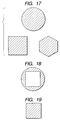
- the electrodes 1606 and 1607 are positioned inside the electrodes 1604 and 1605, respectively, in the region other than the periphery of the single-crystal silicon substrate 1301 and in the form of, e.g., a disk or polygon as shown in Fig. 17.
- a relatively high electric current is flowed across the electrodes 1604 and 1605 and etching is carried out in an electropolishing mode to remove the silicon layers 1304 and 1305, or the silicon layers 1304 and 1305 and part or the whole of the porous layer 1303, lying on the periphery of the single-crystal silicon substrate 1301.
- the removing of either only the silicon layers 1304 and 1305 or both the silicon layers 1304 and 1305 and part or the whole of the porous layer 1303 may be selected in accordance with the separating strength of the porous layer.
- the silicon layers 1304 and 1305 (304) do not completely cover the porous layer 1303 (303) and the porous layer 1303 is uncovered to the surface of the single-crystal silicon substrate 1301 (wafer), part or the whole of the porous layer 1303 at its uncovered portion is removed.
- a relatively low electric current is flowed across the electrodes 1604 and 1605 to carry out conventional anodizing, and a thin porous layer 1309 is formed on the surface of the silicon layer 1304 in its region other than the peripheral region of the single-crystal silicon substrate 1301 to provide an anti-reflection layer (Fig. 12E).
- the step of removing the silicon layer and porous layer on the periphery and the step of forming the porous layer on the surface of the silicon layer in its region other than the peripheral region may be carried out simultaneously or separately.
- a transparent polymeric-film substrate 1306 is bonded with an adhesive 1307 to the side of the single-crystal silicon substrate 1301 on which the silicon layers 1304 and 1305 have been formed, and these are put in an oven (not shown) and heated to bring the polymeric-film substrate 1306 and the silicon layer 1305 on the single-crystal silicon substrate 1301 into firm bond (Fig. 12F).
- the transparent polymeric-film substrate 1306 and the single-crystal silicon substrate 1301 with the stated layers, thus firmly bonded, are put in a water bath to make ultrasonic waves act thereon (not shown).
- the silicon layer 1304 is separated from the single-crystal silicon substrate 1301 at the part of the porous layer 1303 (Fig. 12G).
- a porous layer 1303a remaining on the silicon layer 1304 separated from the single-crystal silicon substrate 1301 is selectively removed. Only the porous silicon is removed by electroless wet chemical etching by the use of at least one of a usual silicon etchant, porous-silicon selective-etchant hydrofluoric acid, a mixed solution prepared by adding at least one of an alcohol and hydrogen peroxide water to hydrofluoric acid, buffered hydrofluoric acid, a mixed solution prepared by adding at least one of an alcohol and hydrogen peroxide water to buffered hydrofluoric acid, and an alkali solution of KOH, NaOH or hydrazine.
- a usual silicon etchant porous-silicon selective-etchant hydrofluoric acid
- a mixed solution prepared by adding at least one of an alcohol and hydrogen peroxide water to hydrofluoric acid buffered hydrofluoric acid
- a mixed solution prepared by adding at least one of an alcohol and hydrogen peroxide water to buffered hydrofluoric acid and
- a p + -type (or n + -type) layer 1308 is formed and a back electrode 1311 is formed by vacuum deposition to make up a solar cell (Fig. 12H).
- another supporting substrate metal substrate
- the single-crystal silicon substrate 1301 after separation may be treated in the same manner as the above to remove a porous layer 1303b remaining on its surface.
- the surface may optionally be flatted (Fig. 12I), and thereafter the substrate is reused in the step of Fig. 12A.
- the thin-film semiconductor layer and optionally the porous layer lying on the periphery of the separating region are kept removed before the former is bonded to the supporting substrate to which it is to be transferred.
- This enables the separating force to act in a good efficiency at the portion readily separable in the porous layer (inclusive of the interface between it and the substrate or semiconductor layer), and hence enables separation free of any adverse effect such as cracking or breaking of the thin-film semiconductor layer.
- thin-film semiconductor members having good characteristics can be obtained in a good efficiency.
- the thin-film semiconductor layer and optionally the porous layer lying on the periphery of the separating region are kept removed before the former is bonded to the supporting substrate to which it is to be transferred, the anti-reflection layer is kept formed on the surface of the semiconductor layer in the separating region.
- the aqueous HF solution is used, where layer can be made porous when it has an HF concentration of at least 10% by weight.
- the quantity of electric current flowed at the time of anodizing may appropriately be determined in accordance with the HF concentration, the intended layer thickness of the porous silicon layer and the state of porous layer surface. Stated roughly, it may suitably be within the range of from 1 mA/cm 2 to 100 mA/cm 2 .
- the level of anodizing electric current may be changed. This makes it possible to previously provide the porous layer with a structural change in density.
- its porous structure can be made plural into two or more layers to enable easy separation.
- the quantity of the alcohol to be added may appropriately be determined in accordance with the HF concentration, the intended layer thickness of the porous silicon layer and the state of porous layer surface. It must be determined especially while paying attention not to make the HF concentration too low.
- the electric currents applied across the electrodes for removing the peripheral portion and across the electrodes for forming the anti-reflection layer may preferably independently be controlled.
- the form of the electrodes those having forms as shown in Figs. 16 and 17 may preferably be used which are fitted to the form the substrate to be treated has, and the electrodes for forming the anti-reflection layer may preferably be so disposed as to be inside the electrodes for removing the peripheral portion.
- a form in which the middle area of a disk has been hollowed out in square as shown in Fig. 18 and a form corresponding substantially to the hollowed-out square as shown in Fig. 19 may be employed in the electrodes for removing the peripheral portion and the electrodes for forming the anti-reflection layer, respectively.
- a semiconductor layer having a square form can be separated from a substrate having the form of a round wafer.
- materials for the electrodes there are no prescriptions on those for the anode side, but those endurable to acids such as hydrofluoric acid are preferred for those on the cathode side, and platinum may most preferably be used.
- An anodizing apparatus having an isolator 1412 (having a cross-sectional form corresponding to the form of the electrodes for forming the anti-reflection layer) as shown in Fig. 13 may also be used for the purpose of improving the independency of electric current control between the electrodes for removing the peripheral portion and between the electrodes for forming the anti-reflection layer.
- the cathode-side electrode is disposed at a position close to the substrate as far as possible in order to make a loss less occur and the distance between the electrodes is shorter than that between the electrodes for forming the anti-reflection layer.
- the electrode on the cathode side may be at any desired distance to the substrate (see Figs. 13 to 15).
- the etching can be effected at an HF concentration of at least 20% by weight when silicon is etched with the aqueous HF solution.
- electroconductivity-providing agents including alcohols such as ethyl alcohol, water, acids or salts thereof may be used.
- the quantity of electric current flowed here may appropriately be determined in accordance with the HF concentration. Stated roughly, it may suitably be within the range of from 10 mA/cm 2 to 100 mA/cm 2 .
- the crystal growth process used in the present invention to form the silicon layer on the porous layer may include thermal CVD, LPCVD (low-pressure CVD), sputtering, plasma CVD, photo-assisted CVD, and liquid-phase epitaxy.
- material gases used in the case of, e.g., gas-phase epitaxy such as the thermal CVD, LPCVD, plasma CVD or photo-assisted CVD they may typically include silanes such as SiH 2 Cl 2 , SiCl 4 , SiHCl 3 , SiH 4 , Si 2 H 6 , SiH 2 F 2 and Si 2 F 6 , and halogenated silanes.
- hydrogen is added as a carrier gas or for the purpose of providing a reducing atmosphere to accelerate crystal growth.
- the proportion of the material gases and hydrogen may appropriately be determined in accordance with the methods of formation, the types of material gases and also the conditions for formation. It may suitably be from 1:10 to 1:1,000 (feed flow rate ratio), and more preferably from 1:20 to 1:800.
- silicon is dissolved in a solvent such as Ga, In, Sb, Bi or Sn to effect epitaxial growth while cooling the solvent gradually or providing a temperature difference in the solvent.
- a solvent such as Ga, In, Sb, Bi or Sn
- temperature and pressure in the epitaxial growth process used in the present invention may differ depending on the methods of formation and the types of materials (gases) used.
- the temperature it may suitably be from 800°C to 1,250°C in approximation when silicon is grown by usual thermal CVD, and may more preferably be controlled to from 850°C to 1,200°C.
- the temperature depends on the types of the solvent, and may preferably be controlled to from 600°C to 1,050C when silicon is grown using Sn or In as the solvent.
- low-temperature processes such as plasma CVD, it may suitably be from 200°C to 600°C in approximation, and may more preferably be controlled to from 200°C to 500°C.
- the pressure it may suitably be from 10 -2 Torr to 760 Torr in approximation, and more preferably be within the range of from 10 -1 Torr to 760 Torr.
- the substrate to which the thin-film crystal semiconductor layer is transferred in the process of the present invention may be any of those having a rigidity and those having a plasticity.
- it may include silicon wafers, SUS stainless steel sheets, glass sheets, and plastic or resin films.
- resin film materials polymeric films may preferably be used, including as typical ones polyimide film, EVA (ethylene vinyl acetate) film, and Tefzel.
- a method may preferably be used in which a conductive metal paste such as copper paste or silver paste, a mixture of such a conductive metal paste with glass frit, or an epoxy type adhesive is inserted between the both to bring them into adhesion, followed by burning to effect firm bond.
- the metal such as copper or silver sintered by burning functions also as a back electrode and a back reflection layer.
- the substrate and the thin-film crystal semiconductor layer are brought into adhesion and in this state (here, a back electrode is previously formed on the surface of the thin-film crystal semiconductor layer) the temperature is raised to the softening point of the film substrate to bond the both firmly.
- Methods for separating the semiconductor layer whose peripheral portion has been removed include a method in which a mechanical external force is made to act directly between the substrates to make separation at the part of the porous layer as a separating layer, and a method in which force (internal stress) existing in the semiconductor layer and separating layer, or between these and the substrate, or energy such as heat, ultrasonic waves, electromagnetic waves or centrifugal force applied externally is utilized and made to act indirectly on a brittle portion in the separating layer.
- the surface of the semiconductor layer may be subjected to texture treatment in order to make incident light less reflect.
- the treatment is made using hydrazine, NaOH or KOH.
- the height of pyramids of the texture formed may suitably be within the range of from several microns to tens of microns.
- the present Example concerns production of a thin-film solar cell according to the process shown in Figs. 1A to 1H.
- a p-type single-crystal silicon substrate (wafer) 101 of 800 ⁇ m thick and 4 inches diameter B (boron) was introduced by thermal diffusion to form a p + -type layer 102.
- This substrate was subjected to anodizing in the state its side on which the p + -type layer was not formed was shielded from an anodizing solution and while changing electric currents into two stages, to obtain a porous layer 103 of about 13 ⁇ m thick.
- the electric currents were first flowed at 8 mA/cm 2 for 10 minutes and thereafter flowed at 30 mA/cm 2 for 1 minute. Because of the changing of electric currents, the porous layer was formed in double-layer structure consisting of a porous layer with a dense structure and a porous layer with a coarse structure.
- the p-type single-crystal silicon wafer 101 at the surface of which the porous layer 103 was formed was annealed at a surface temperature of 1,050°C for 1 minute in an atmosphere of hydrogen, and was thereafter immersed in a 900°C metallic solution of indium into which silicon had been dissolved to become supersaturated, followed by slow cooling to form the silicon layer 104 in a thickness of 30 ⁇ m.
- a cover was provided on the porous layer such that the silicon layer 104 was formed only in the region of a concentric circle smaller by 7 mm in diameter than the wafer.
- P phosphorus
- nine solar-cell regions each having an area of 1 cm 2 were fabricated at the central portion of the silicon layer 104 by isolation of the n + -type layer, and an electrode and an anti-reflection layer were further formed.
- the silicon substrate 101 with these was set in a chamber of a reactive ion etching apparatus, and a glass protective mask of 90 mm diameter was placed thereon in center alignment with the wafer. The portion protruded from the glass mask was etched on the surface side of the silicon layer to remove the silicon layer and part of the porous layer at that portion.
- a transparent adhesive 105 was coated on the surface of the remaining silicon layer 104 such that it was not forced out to the portion uncovered after removal as well as the side (lateral surface) uncovered after removal, and then a transparent substrate 106 was firmly bonded thereto. Thereafter, force was made to act on the porous layer to separate the silicon layer 104 from the silicon substrate 101, and a back electrode was formed to make up a solar cell.
- the present Example concerns production of a semiconductor member according to the process shown in Figs. 2A to 2H.
- a porous layer 203 of about 13 ⁇ m thick was formed in the same manner as in Example 1 except that a p + -type layer 202 was formed at the surface of a p-type silicon substrate (wafer) 201 of 5 inches diameter and the wafer was shielded from the anodizing solution on its periphery 5 mm inward the semiconductor growth surface from the peripheral edge of the wafer. Thereafter, a silicon semiconductor layer 204 of 0.5 ⁇ m thick was epitaxially grown by CVD. (Figs. 2A to 2C).
- the surface layer of the semiconductor layer 204 was subjected to thermal oxidation to form an SiO 2 layer, and thereafter a same-type quartz glass substrate 206 having a diameter smaller by 15 mm than the silicon substrate 201 was bonded thereto in its center alignment with the wafer under heat treatment at 700°C for 0.5 hours (Fig. 2D). Then the portion protruded from the glass substrate 206 (i.e., part of the semiconductor layer 204, part of the porous layer 203 and the semiconductor layer 202) was removed by reactive ion etching (Fig. 2E). It was removed in a depth of about 23 ⁇ m from the surface on the side of the substrate.
- the glass substrate 206 was irradiated with ultrasonic waves to break the porous layer 203 to effect separation, so that the thin-film semiconductor layer was transferred onto the glass substrate 206. Also, a porous residue 207 remaining on the surface of the semiconductor layer 204 was removed by etching to obtain an SOI (silicon-on-insulator) member 208.
- SOI silicon-on-insulator
- an n + -type semiconductor layer of about 0.2 ⁇ m thick and a p - -type semiconductor layer of 30 ⁇ m were successively epitaxially grown by immersing the wafer with porous layer in liquid-phase epitaxy solutions in which impurities suited respectively to these layers had been dissolved.
- the etching was carried out using a jig as shown in Fig. 5.
- a holder 503 is joined to wafer holders (not shown) so that the wafer can be held between them.
- the main body of the jig also has the function to enable adjustment of height so that only the portion intended to be etched is immersed in the etchant.
- Porous residues having remained on the wafer surfaces after the liquid-phase epitaxial thin films were separated were also removed, and the wafer was again subjected to the like steps. As a result, solar cells having a high conversion efficiency were obtainable without any problem.
- a single-crystal silicon wafer 601 (Fig. 6) of 1 mm thick and 5 inches diameter was subjected to anodizing under the same conditions as in Example 3 to form a porous layer 602 of 12 ⁇ m thick in double-layer structure.
- the same wafer as the above on one side of which a porous layer was formed in the same way was additionally prepared. These two wafers were closely put together face to face on their side opposite to the side on which the porous layer was formed, and their periphery was covered and fixed with a jig such that any liquid-phase epitaxy solution did not enter their side on which the porous layer was not formed. These were immersed in a liquid-phase epitaxy solution to grow a p - -type semiconductor layer 603 epitaxially in a thickness of about 40 ⁇ m on each porous layer.
- a comb-like pattern 604 with fingers of 80 ⁇ m wide and 100 ⁇ m in pitch which extended form a bus bar of 3 mm wide was formed by screen printing using a paste containing aluminum.
- the aluminum-silicon contact surface and its vicinity was made into alloy at 900°C to form a p + -type layer 605 and simultaneously the whole surface was oxidized. Only the part where silicon surface was oxidized was selectively removed by etching without removing oxide film 606 of aluminum. Thereafter, an n + -type semiconductor layer 607 was deposited on the surface by CVD.
- the region where the pattern of p + -type layer 605 and n + -type layer 607 was formed was bonded with a conductive paste 608, to a supporting substrate 609 (701 in Fig. 7) of 77 mm ⁇ 77 mm made of stainless steel.
- the semiconductor layer at its portion 702 protruded from the supporting substrate was removed by grinding and polishing. After this removal, a tensile force was applied to the interface between the supporting substrate made of stainless steel and the wafer to separate the thin-film semiconductor layer. A porous residue having remained on the thin-film semiconductor layer was removed and an anti-reflection layer was formed.
- back-side junction-concentrated type solar cells were produced.
- a porous layer was formed in the same manner as in Example 1. Thereafter, on the porous layer, a p + -type semiconductor layer of about 1 ⁇ m thick and a p - -type semiconductor layer of 30 ⁇ m thick were successively epitaxially grown by liquid-phase growth in the same manner as in Example 4, by immersing the wafer with porous layer in liquid-phase epitaxy solutions in which impurities suited respectively to these layers had been dissolved. Thereafter, a diffusing agent was coated on the surface of the p - -type semiconductor layer, followed by heat treatment to form an n + -type layer.
- the n + -type layer, formed on the whole surface was subjected to isolation in a region 801 (Fig. 8) of 85 mm ⁇ 85 mm. Then an electrode pattern was printed with a silver paste on the surface of the n + -type layer, and an insulating anti-reflection layer was further deposited thereon.
- the semiconductor layer and porous layer were removed in a depth of 45 ⁇ m in parallel to a pair of opposing sides of the square region 801 formed by isolation as shown in Fig. 8, and in regions 802 set apart by 5 mm from isolation lines.
- a transparent adhesive was so coated as not to come around to the portion uncovered after removal with the laser, and a transparent substrate was bonded to the semiconductor layer. Then, force was applied to the substrate to cause separation to progress in the direction parallel to the side regions removed by the laser. Thus, the semiconductor layer was transferred to the transparent substrate, followed by formation of a back electrode to obtain a solar cell.
- a single-crystal silicon wafer 901 (Fig. 9) of 1 mm thick and 5 inches diameter was subjected to anodizing under the same conditions as in Example 1 to form a porous layer 902 of 12 ⁇ m thick in double-layer structure.
- the same wafer as the above on one side of which a porous layer was formed in the same way was additionally prepared. These two wafers were closely put together face to face on their side opposite to the side on which the porous layer was formed, and their periphery was covered and fixed with a jig such that any liquid-phase epitaxy solution did not enter their contact surface. These were immersed in a liquid-phase epitaxy solution to grow a p - -type semiconductor layer (silicon layer) 903 epitaxially in a thickness of about 40 ⁇ m on each porous layer.
- each silicon layer P (phosphorus) was diffused to form an n + -type layer, and thereafter nine solar-cell regions each having an area of 1 cm 2 were fabricated at the central portion of the silicon layer by isolation of the n + -type layer, and an electrode and an anti-reflection layer were further formed.
- P phosphorus
- a glass substrate 905 of the same type as the silicon wafer was bonded with a transparent adhesive 904.
- the quantity of the adhesive was so controlled that the adhesive did not come around to the edge face of the wafer.
- a fluid 906 of mixture of fine glass beads with pure water was jetted at a jet-out pressure of 1.0 to 2.0 kg/cm 2 by means of a honing apparatus.
- the porous layer formed at the edge of the wafer was removed over the whole periphery of the wafer.
- the glass substrate was provided with a mask tape 907 so as not to be scratched.
- the present Example concerns production of a semiconductor member by transferring a single-crystal silicon layer to a glass substrate according to the process shown in Figs. 10A to 10H.
- boron was thermally diffused using BCl 3 as a thermal diffusion source at a temperature of 1,200°C to form a p + -type layer to obtain a diffusion layer 1102 of about 3 ⁇ m thick (Fig. 10A).
- This wafer whose surface layer 1102 became p + -type was subjected to anodizing in an aqueous HF/C 2 H 5 OH solution under conditions shown in Table 1 (Fig. 10B).
- the anodizing was carried out first at a low electric current of 8 mA/cm 2 for 2.5 minutes and thereafter, slowly raising the level of electric current on, the anodizing was stopped at the time the electric current reached 35 mA/cm 2 in 30 seconds.
- the porous layer 1103 formed was in a layer thickness of about 3 ⁇ m in total.
- Anodizing solution HF:H 2 O:C 2 H 5 OH 1:1:1 Current density 8 mA/cm 2 ⁇ 35 mA/cm 2 Anodizing time 2.5 min ⁇ (30 sec.) ⁇ 0 sec.
- a silicon layer 1104 was formed in a thickness of 0.5 ⁇ m by thermal CVD (Fig. 10C).
- the peripheral portion of the wafer was in such a state that the silicon layer 1104 covered the top of the porous layer 1103 like that shown in Fig. 3A.
- the wafer 1101 with porous layer was set in the anodizing apparatus shown in Fig. 14, at its prescribed position such that the silicon layer 1104 faced a negative electrode 1504 in the aqueous HF solution.
- the negative electrode 1504 had substantially the same form as a positive electrode 1505 coming in contact with the back of the wafer 1101, and was provided along the periphery of the wafer 1101 in the form of a beltlike ring (see Fig. 16).
- an oxide film 1106 was formed in a thickness of 0.1 ⁇ m by normal-pressure CVD at 450°C. Thereafter, a glass substrate 1105 was bonded to the oxide film 1106, and these were put in a heat-treating furnace (not shown) and heated at 1,150°C to bring the glass substrate 1105 and the silicon layer 1104 on the wafer 1101 into firm bond (Fig. 10E).
- a porous layer 1103a remaining on the silicon layer 1104 separated from the wafer 1101 was selectively removed with a solution of HF/H 2 O mixture.
- a solution of HF/H 2 O mixture was selectively removed with a solution of HF/H 2 O mixture.
- the wafer 1101 after separation was treated in the same manner as the above to remove a porous layer 1103b remaining on its surface.
- the surface was optionally flatted by polishing or the like (Fig. 10H).
- the present Example concerns production of a solar cell by transferring a thin-film single-crystal silicon layer to a polyimide film according to the process shown in Figs. 11A to 11I.
- boron was thermally diffused using BCl 3 as a thermal diffusion source at a temperature of 1,200°C to form a p + -type layer to obtain a diffusion layer 1202 of about 3 ⁇ m thick (Fig. 11A).
- This wafer whose surface layer 1202 became p + -type was subjected to anodizing in an aqueous HF/C 2 H 5 OH solution under conditions shown in Table 2.
- the anodizing was carried out first at a low electric current of 8 mA/cm 2 for 10 minutes and thereafter, raising the level of electric current, an electric current was flowed at 30 mA/cm 2 for 1 minute.
- the porous layer 1203 formed was in a layer thickness of about 13 ⁇ m in total.
- Anodizing solution HF:H 2 O:C 2 H 5 OH 1:1:1 Current density 8 mA/cm 2 ⁇ 30 mA/cm 2 Anodizing time 10 min ⁇ (0 sec.) ⁇ 1 min.
- a silicon layer 1204 was formed in a thickness of 30 ⁇ m by epitaxial growth carried out under conditions shown in Table 3, by means of a liquid-phase epitaxy system of a slider type making use of indium as a solvent.
- boron was added in the solvent in a trace quantity (approximately zero-point-few ppm to few ppm based on the weight of silicon dissolved therein) to make the grown silicon layer 1204 into p - -type and also, after the growth was completed, a p + -type layer 1205 was further formed on grown silicon layer 1204 in a thickness of 1 ⁇ m, using another indium melt having a larger boron content (at least hundreds of ppm based on the weight of silicon dissolved therein) (Figs. 11C, 11D).
- the wafer 1201 with porous layer was set in the anodizing apparatus shown in Fig. 14, at its prescribed position such that the silicon layer 1204 faced a negative electrode 1504 in the aqueous HF solution.
- the negative electrode 1504 had substantially the same form as a positive electrode 1505 coming in contact with the back of the wafer 1201, and was provided along the periphery of the wafer 1201 in the form of a beltlike ring (see Fig. 16).
- a silver paste 1207 was coated in a thickness of 10 to 30 ⁇ m by screen printing, and this side was brought into close contact with the p + -type silicon layer 1205 side to effect bonding. In this state, these were put in an oven, where the silver paste was sintered under conditions of 360°C for 20 minutes and also the polyimide film 1206 and the silicon layer 1205 on the wafer 1201 into firm bond (Fig. 11F).
- a porous layer 1203a remaining on the silicon layer 1204 separated from the wafer 1201 was selectively etched with a solution of HF/H 2 O 2 /H 2 O mixture with stirring. The silicon layers remained without being etched and only the porous layer was completely removed.
- the ⁇ c-Si layer had a dark conductivity of ⁇ 5 S / cm.
- Gas flow rate ratio SiH 4 /H 2 1 cc/20 cc PH 3 /SiH 4 2.0 ⁇ 10 -3
- an ITO (indium tin oxide) transparent conductive film 1209 (82 nm) and a collector electrode 1210 (Ti/Pd/Ag: 400 nm/200 nm/1 ⁇ m) were formed by EB (electron beam) vacuum deposition to make up a solar cell (Fig. 11H).
- porous layer remaining on the silicon wafer after separating was also removed by etching in the same manner as the above, and its surface was made flat (Fig. 11I). Using the regenerated wafer thus obtained, the above steps were repeated to obtain a plurality of thin-film single-crystal solar cells having high-quality semiconductor layers.
- the present Example concerns production of a solar cell by transferring a polycrystalline silicon layer to a Tefzel film (transparent film) according to the process shown in Figs. 12A to 12I.
- boron was thermally diffused using BCl 3 as a thermal diffusion source at a temperature of 1,200°C to form a p + -type layer 1302 to obtain a diffusion layer of about 3 ⁇ m thick (Fig. 12A).
- anodizing was carried out in an aqueous HF solution under conditions shown in Table 5, to form a porous silicon layer 1303 at the surface of the wafer (Fig. 12B).
- the anodizing was carried out first at a low electric current of 5 mA/cm 2 for 2.5 minutes and thereafter, slowly raising the level of electric current on, the anodizing was stopped at the time the electric current reached 32 mA/cm 2 in 30 seconds.
- Anodizing solution HF:H 2 O:C 2 H 5 OH 1:1:1 Current density 5 mA/cm 2 ⁇ 32 mA/cm 2
- Anodizing time 2.5 min. ⁇ (30 sec.) ⁇ 0 sec.
- a silicon layer (polycrystalline) was formed in a layer thickness of about 30 ⁇ m by crystal growth carried out under conditions shown in Table 6, by means of a conventional thermal CVD system.
- Gas flow rate ratio SiH 4 Cl 2 /H 2 0.5/100 (1/min.)
- ppm to few ppm of B 2 H 6 was added to make the grown silicon layer into p - -type and also, at the final stage of the growth, hundreds of ppm of PH 3 was added in place of B 2 H 6 to form an n + -layer 1305 in a thickness of 0.2 ⁇ m to form a p-n junction (Fig. 12C, 12D).
- the peripheral portion of the wafer was in such a state that the silicon layer 1304 covered the top of the porous layer 1303 like that shown in Fig. 3A.
- the wafer 1301 with porous layer was set in the anodizing apparatus shown in Fig. 15, at its prescribed position such that the silicon layer 1305 faced a negative electrodes 1604 and 1606 in the aqueous HF solution.
- the negative electrodes 1604 and 1606 had substantially the same form as positive electrodes 1605 and 1607, respectively, coming in contact with the back of the wafer 1301.
- the electrodes 1604 and 1605 were provided along the periphery of the wafer 1301 in the form of a beltlike rectangle (square) (see Fig. 16).
- the electrodes 1606 and 1607 were provided inside the electrodes 1604 and 1605, respectively, in the region other than the periphery of the wafer 1301 in the form of a rectangle (square) (see Fig. 17).
- an ITO transparent conductive film (not shown) (82 nm) and a collector electrode 1310 (Ti/Pd/Ag: 400 nm/200 nm/1 ⁇ m) were formed by EB vacuum deposition to make up a solar cell previously.
- a transparent adhesive 1307 was coated in a thickness of 10 to 30 ⁇ m, and this side was brought into close contact with the transparent conductive film/collector electrode surface to effect bonding (Fig. 12F).
- the Tefzel film 1306 and wafer 1301 brought into a bonded structure were fastened with a vacuum chuck (not shown) on the latter's side not bonded to the former, in the state of which force was made to act from one edge of the Tefzel film 1306.
- the flexibility of the Tefzel film was utilized and the both were slowly drawn off from an edge of the wafer 1301 to effect separating.
- the silicon layers 1304 and 1305 were separated from the wafer 1301 at the part of the porous layer 1303 and transferred onto the Tefzel film 1306 (Fig. 12G). Neither cracks nor breaks were seen on the periphery of the silicon layers thus separated.
- a porous layer 1303a remaining on the silicon layer 1304 separated from the polycrystalline silicon wafer 1301 was selectively etched with an aqueous KOH solution of 1% by weight in concentration with stirring.
- the silicon layer 1304 remained without being etched so much and the porous layer was completely removed.
- a p-type ⁇ c-Si layer was deposited in a thickness of 500 angstroms by plasma CVD under conditions shown in Table 7.
- the ⁇ c-Si layer had a dark conductivity of ⁇ 1 S/cm.
- a back electrode 1311 aluminum was also deposited in a thickness of 0.1 ⁇ m by sputtering, and a SUS stainless steel substrate (not shown) was further bonded as a supporting substrate via a conductive adhesive to obtain a solar cell (Fig. 12H).
- porous layer remaining on the silicon wafer after separating was also removed by etching in the same manner as the above, and its surface was made flat (Fig. 12I). Using the regenerated wafer thus obtained, the above steps were repeated to obtain a plurality of thin-film polycrystalline solar cells having high-quality semiconductor layers.
- the present Example concerns production of a solar cell according to the process shown in Figs. 11A to 11I where a form in which the middle area of a disk has been hollowed out in square as shown in Fig. 18 and a form corresponding substantially to the hollowed-out square as shown in Fig. 19 are employed in the electrodes for removing the peripheral portion and the electrodes for forming the anti-reflection layer, respectively.
- boron was thermally diffused in the same manner as in Examples 7 to 9, using BCl 3 as a thermal diffusion source at a temperature of 1,200°C to form a p + -type layer to obtain a diffusion layer 1202 of about 3 ⁇ m thick (Fig. 11A).
- This wafer whose surface layer 1202 became p + -type was subjected to anodizing in an aqueous HF/C 2 H 5 OH solution under conditions shown in Table 2 to form a porous layer 1203 at the surface of the wafer (Fig. 11B).
- the anodizing was carried out first at a low electric current of 8 mA/cm 2 for 10 minutes and thereafter, raising the level of electric current, an electric current was flowed at 30 mA/cm 2 for 1 minute.
- the porous layer 1203 formed was in a layer thickness of about 13 ⁇ m in total.
- a silicon layer 1204 (single crystal) was formed in a layer thickness of about 30 ⁇ m by epitaxial growth carried out under conditions shown in Table 6, by means of a conventional thermal CVD system.
- zero-point-few ppm to few ppm of B 2 H 6 was added to make the grown silicon layer into p + -type and also, at the final stage of the growth, the B 2 H 6 was increased to hundreds of ppm or more to form a p + -layer 1205 in a thickness of 1 ⁇ m (Figs. 11C, 11D).
- the peripheral portion of the wafer was in such a state that the silicon layer 1204 covered the top of the porous layer 1203 like that shown in Fig. 3A.
- the wafer 1201 with porous layer was set in the anodizing apparatus shown in Fig. 15, at its prescribed position such that the silicon layer 1205 faced negative electrodes 1604 and 1606 in the aqueous HF solution.
- the negative electrodes 1604 and 1606 had substantially the same form as positive electrodes 1605 and 1607, respectively, coming in contact with the back of the wafer 1201.
- the electrodes 1604 and 1605 were provided along the periphery of the wafer 1201 in the form of a disk the middle area of which had been hollowed out in square (see Fig. 18).
- the electrodes 1606 and 1607 were provided inside the electrodes 1604 and 1605, respectively, in the region other than the periphery of the wafer 1201 in the form corresponding substantially to the hollowed-out square (see Fig. 19).
- a silver paste 1207 was coated in a thickness of 10 to 30 ⁇ m by screen printing, and this side was brought into close contact with the p + -type silicon layer 1205 side to effect bonding. In this state, these were put in an oven, where the silver paste was burnt under conditions of 360°C for 20 minutes and also the polyimide film 1206 and the silicon layer 1205 on the wafer 1201 into firm bond (Fig. 11F).
- an energy of ultrasonic waves was applied in a water bath.
- the silicon layers were separated from the wafer at the part of the porous layer.
- the silicon layers 1204 and 1205 of about 125 mm square were separated from the round wafer of 8 inches diameter and transferred onto the polyimide film 1206 (Fig. 11G). Neither cracks nor breaks were seen on the periphery of the silicon layers thus separated.
- a porous layer 1203a remaining on the silicon layer 1204 separated from the wafer 1201 was selectively etched with a solution of HF/H 2 O 2 /H 2 O mixture with stirring. The silicon layers remained without being etched and only the porous layer was completely removed.
- the ⁇ c-Si layer had a dark conductivity of ⁇ 5 S/cm.
- an ITO transparent conductive film 1209 (82 nm) and a collector electrode 1210 (Ti/Pd/Ag: 400 nm/200 nm/1 ⁇ m) were formed by EB vacuum deposition to make up a solar cell (Fig. 11H).
- porous layer remaining on the silicon wafer after separating was also removed by etching in the same manner as the above, and its surface was made flat (Fig. 11I). Using the regenerated wafer thus obtained, the above steps were repeated to obtain a plurality of thin-film single-crystal solar cells having high-quality semiconductor layers.
- the present invention has specifically been described above by giving Examples.
- the present invention is by no means construed limitative by the foregoing Examples, and is modifiable in variety.
- the foregoing description concerns production of solar cells by separating rectangular semiconductor layers from round-wafer type substrates, but the form of the electrodes for removing the peripheral portion and electrodes for forming the anti-reflection layer can be set as desired, and hence semiconductor layers having any desired forms can be separated from substrates having any desired forms.
- the porous layer is utilized as a separating layer, but a semiconductor member having a separating layer formed by providing a brittle portion in the interior of the wafer can also be treated in quite the same manner as the above, by, e.g., implanting H ions or He ions in the silicon wafer to make heat treatment.
- H ions are implanted into the surface portion of the crystal silicon substrate under conditions of 20 keV and 5 ⁇ 10 16 cm 2 to form the brittle layer in a depth of 0.1 ⁇ m from the silicon surface, and the silicon layer is formed thereon by thermal CVD in the same manner as in, e.g., Example 7. Thereafter, the removal of peripheral portion, the separating and so forth may be followed up likewise according to the steps of, e.g., Figs. 10D to 10H.
- the present invention has made it possible to obtain in a good efficiency semiconductor members and thin-film crystal solar cells having less cracks or breaks and good characteristics. This has made it possible to provide in the market semiconductor members and solar cells having mass productivity and good quality.
- the present invention also has made it possible to form through simple steps thin-film crystal solar cells having good characteristics, making it possible to produce inexpensive solar cells.
- the present invention still also has made it possible to form with ease semiconductor members and thin-film crystal solar cells having any desired forms.
- the process comprises the steps of: (1) anodizing the surface of a first substrate to form a porous layer at least on one side of the substrate, (2) forming a semiconductor layer at least on the surface of the porous layer, (3) removing the semiconductor layer at its peripheral region, (4) bonding a second substrate to the surface of the semiconductor layer, (5) separating the semiconductor layer from the first substrate at the part of the porous layer, and (6) treating the surface of the first substrate after separation and repeating the above steps (1) to (5).
- This process enables separation of the thin-film semiconductor layer at a small force while causing less cracks, breaks or defects to be brought into it and can manufacture high-performance semiconductor members and solar cells in a good efficiency.
Abstract
In a process for producing a semiconductor member,
and a solar cell, making use of a thin-film crystal
semiconductor layer, the process comprises the steps
of: (1) anodizing the surface of a first substrate to
form a porous layer at least on one side of the
substrate, (2) forming a semiconductor layer at least
on the surface of the porous layer, (3) removing the
semiconductor layer at its peripheral region, (4)
bonding a second substrate to the surface of the
semiconductor layer, (5) separating the semiconductor
layer from the first substrate at the part of the
porous layer, and (6) treating the surface of the first
substrate after separation and repeating the above
steps (1) to (5).
This process enables separation of the thin-film
semiconductor layer at a small force while causing less
cracks, breaks or defects to be brought into it and can
manufacture high-performance semiconductor members and
solar cells in a good efficiency.
Description
This invention relates to a method of separating a
semiconductor thin film deposited on a porous layer, a
process for producing a semiconductor member, a process
for producing a solar cell formed of a thin-film single
crystal layered on a low-cost substrate, and an
anodizing apparatus used in these.
A technique is known in which a thin-film
semiconductor layer is formed on a porous layer formed
at the surface portion or layer of a semiconductor
substrate and thereafter the semiconductor layer is
separated at the part of the porous layer. As a
separation method, used is a chemical method making use
of etching or a physical method of causing ultrasonic
waves or force such as tensile force to act on.
With regard to the physical method, Japanese
Patent Application Laid-Open No. 7-302889 discloses
that a porous layer is formed at the surface of a
silicon wafer, thereafter an epitaxial growth layer is
formed thereon, another wafer is bonded to the
epitaxial growth layer (silicon layer), and a pressure,
a shear force or ultrasonic waves is/are applied to the
porous layer to make separation. Japanese Patent
Application Laid-Open No. 8-213645 also discloses that
a porous layer is formed at the surface of a
single-crystal silicon substrate, thereafter a p-n
junction layer is formed thereon, the single-crystal
silicon substrate is, on its back, fastened to a jig
through an adhesive, another jig is bonded to the
epitaxial growth layer, and both the jigs are pulled
against each other to cause the porous layer to break
to obtain a thin-film epitaxial growth layer (a solar
cell). Japanese Patent Application Laid-Open No.
10-190032 discloses that a difference in shrink between
a silicon layer and a plastic substrate bonded to the
silicon layer is utilized to separate the former from
the latter by cooling them with a vapor of liquid
nitrogen.
However, when the thin-film epitaxial growth layer
is obtained by separating it at the part of the porous
layer, the thin-film semiconductor layer may finely be
cracked or broken on the periphery of a region where it
is to be separated (i.e., a separating region), because
of an impact produced when the porous layer formed at
the surface of the first substrate is broken by
separating force. Where it is thus cracked or broken,
not only the thin film can be handled with difficulty
but also, when cracked or broken up to the central
area, the yield and characteristics of devices
including solar cells may lower.
An object of the present invention is to provide a
process for producing a semiconductor member and a
solar cell, which process enables separation of the
thin-film semiconductor layer at a small force while
causing less cracks, breaks or defects to be brought
into it and can manufacture high-performance
semiconductor members and solar cells in a good
efficiency.
To achieve the above object, the present invention
provides a process for producing a semiconductor member
making use of a thin-film crystal semiconductor layer,
the process comprising the steps of:
The present invention also provides a process for
producing a semiconductor member making use of a
thin-film crystal semiconductor layer, the process
comprising the steps of:
The present invention still also provides a
process for producing a solar cell making use of a
thin-film crystal semiconductor layer, the process
comprising the steps of:
The present invention further provides a process
for producing a solar cell making use of a thin-film
crystal semiconductor layer, the process comprising the
steps of:
The present invention still further provides a
process for producing a semiconductor member obtained
by separating a thin-film crystal semiconductor layer
formed on a first substrate to transfer the former to a
second substrate, wherein the thin-film crystal
semiconductor layer is removed by etching by
electropolishing at its part on the periphery of the
first substrate.
The present invention still further provides a
process for producing a semiconductor member making use
of a thin-film crystal semiconductor layer, the process
comprising the steps of:
The present invention still further provides a
process for producing a solar cell obtained by
separating a thin-film crystal semiconductor layer
formed on a first substrate to transfer the former to a
second substrate, wherein the thin-film crystal
semiconductor layer is removed by etching by
electropolishing at its part on the periphery of the
first substrate.
The present invention still further provides a
process for producing a solar cell making use of a
thin-film crystal semiconductor layer, the process
comprising the steps of:
The present invention still further provides an
anodizing apparatus comprising, at the peripheral
portion of a substrate to be subjected to anodizing, a
first electrode coming in contact with the back side of
the substrate and a second electrode facing the first
electrode, interposing the substrate between them; the
first electrode having substantially the same form as
the second electrode.
The present invention still further provides an
anodizing apparatus comprising, at the peripheral
portion of a substrate to be subjected to anodizing, a
first electrode coming in contact with the back side of
the substrate and a second electrode facing the first
electrode, interposing the substrate between them, and,
in the remaining substrate region excluding the
peripheral portion, a third electrode coming in contact
with the back side of the substrate and a fourth
electrode facing the third electrode, interposing the
substrate between them; the first electrode and third
electrode having substantially the same form as the
second electrode and fourth electrode, respectively.
Embodiments of the present invention will be
described below in detail.
As an embodiment according to the present
invention, a process for producing a semiconductor
member is described with reference to Figs. 1A to 1H.
Into the surface portion or layer of a
first-substrate crystal substrate as exemplified by a
single-crystal silicon wafer 101, impurities are
introduced by thermal diffusion or ion implantation or
are incorporated when the wafer is produced, to form a
p+-type (or n+-type) layer 102 at least at the wafer
surface (Fig. 1A).
Next, the wafer surface on the side the impurities
have been introduced is subjected to anodizing in,
e.g., an aqueous HF (hydrogen fluoride) solution to
make the surface and the vicinity thereof porous to
form a porous layer 103 (Fig. 1B).
This porous layer 103 is subjected to hydrogen
annealing to make its surface smooth, followed by CVD
(chemical vapor deposition) or liquid-phase epitaxial
growth to grow a single-crystal silicon semiconductor
layer 104 (Fig. 1C).
In the course of the anodizing to make porous, the
level of anodizing electric current may be changed,
e.g., from a low level to a high level. This makes it
possible to previously provide the porous layer with a
structural change in density, whereby after epitaxial
growth the semiconductor layer 104 can be separated
(peeled) from the silicon wafer 101 with ease at the
part of the porous layer.
Where the side of a wafer on which the
semiconductor layer is formed is defined to be the
surface and the other side the back, the semiconductor
layer 104 formed on the porous layer 103 comes as
follows: When, e.g., the surface portion is made
porous in the state the periphery of the surface is
shielded from the anodizing solution at the time of
anodizing, and the epitaxial growth is carried out on
the whole surface, what is formed in and on the wafer
are, as shown in Fig. 3A, a porous layer 303, a flat
single-crystal layer 305 formed when pores of the
porous-layer surface portion are stopped up as a result
of the hydrogen annealing carried out before the
semiconductor layer is formed, and a single-crystal
silicon semiconductor layer 304 formed by epitaxial
growth. In order to separate the semiconductor layer
to transfer it to a second substrate 308, the
semiconductor layer 304, single-crystal layer 305 and
porous layer 303 must be broken by separating force so
as to reach a portion having the lowest breaking
strength in the porous layer, and at this time the
semiconductor layer 304 tends to be cracked or broken
or to have other defects brought into it.
As another example, when the porous layer is
formed in the state the back is shielded from the
anodizing solution, and the epitaxial growth is carried
out in the state the wafer (with the porous layer) is
masked on the periphery of the surface up to the whole
back, a structure as shown in Fig. 3B comes about. The
porous layer 303 is not hydrogen-annealed at its masked
portion and hence neither flat single-crystal layer 305
nor semiconductor layer 306 is formed at that portion.
In order to separate the semiconductor layer 304 to
transfer it to the second substrate 308, the porous
layer must be broken at its some portion so that the
thin-film single-crystal silicon layer can be separated
at a portion having the lowest breaking strength in the
porous layer. In this case, too, when the porous layer
has a high breaking strength, the single-crystal
silicon layer 304 formed by epitaxial growth may be
damaged like the above case.
Accordingly, depending on the separation strength
of the porous layer, only the single-crystal silicon
layer (silicon layer 104) or, in addition thereto, part
or the whole of the porous layer at its/their
portion(s) lying on the periphery of the separating
region is/are removed (Fig. 1D). Then, a second
substrate supporting substrate 106 is bonded to the
silicon layer 104 via an adhesive layer 105 such that
it is not bonded to the portion uncovered after removal
(Fig. 1E). Thereafter, a physical separating force
(e.g., a direct force such as mechanical force or an
indirect force that acts via a medium, such as
ultrasonic waves) is applied to the porous layer 103 to
separate the silicon layer from the silicon wafer 101
and transfer it onto the supporting substrate 106 (Fig.
1F). In this case, the direct force may directly be
applied to the porous layer 103, or may be applied to
one or both of the wafer 101 and the supporting
substrate 106, or may be applied to all of them.
By doing so, the thin-film semiconductor layer can
be made less broken or damaged and also any force
applied to the porous layer at its portion other than
the part where it is readily separable can be made
small, making it possible to effect separation at a
small force. Here, the silicon layer and optionally
the porous layer may be removed after the supporting
substrate 106 has been bonded. In this case, it is
efficient to use the supporting substrate as a
substitute for a mask necessary for removing the
periphery (see Figs. 2A to 2H). The removing of the
semiconductor layer and optionally the porous layer at
its/their portion(s) lying on the periphery of the
separating region, which may be effective when done at
part of the periphery, can be more effective when done
on the whole periphery.
A porous residue 107 remaining after transfer on
the surface of the thin-film single-crystal silicon
layer may optionally be etched away by etching or the
like to obtain a semiconductor member or solar cell
(Fig. 1G). The supporting substrate used for the
separation of the silicon layer may be incorporated in
the semiconductor member or solar cell product as it
is, or the thin-film silicon may again be transferred
to a third substrate suited for the product.
The silicon wafer 101 from which the silicon layer
has been separated may be treated to remove by etching
or the like the porous residue 107 remaining on its
surface. Thus, it can be reused in the first step and
can effectively be utilized (Fig. 1H).
The removing of the periphery of the separating
region, which is to obtain a thin-film semiconductor
with ease, may be done before the substrate for
supporting the silicon thin film (the supporting
substrate) is bonded or before the supporting substrate
has been bonded. In the case where the periphery of
the separating region is removed before the supporting
substrate is bonded, it is removed by dry etching such
as reactive ion etching, wet etching or electrolytic
etching making use of a hydrofluoric acid type etchant,
mechanical methods such as grinding or polishing, or
laser-assisted etching, in the state the separating
region is masked. Thereafter, the supporting substrate
is bonded to the separating region while paying
attention so as not to provide the adhesive to the
portion uncovered after removal. In the case where the
periphery is removed after the supporting substrate has
been bonded, the supporting substrate for the thin film
may be made to serve as a mask, thereby making good use
of the material and saving the step of removing the
mask, resulting in a good efficiency.
What is removed is only the peripheral region of
the semiconductor layer or, in addition thereto, part
or the whole of the peripheral region of the porous
layer. Since the porous layer may have a different
structure depending on anodizing conditions and may
have a different separation strength, it may be removed
in a depth most suited for the separation.
Features of the process for producing the
semiconductor member and solar cell according to the
present invention will be described below in detail.
The porous layer is described first, taking the
case of silicon as an example. In the anodizing for
forming the porous layer (porous silicon layer) 103,
the aqueous HF solution (hydrofluoric acid) may
preferably be used. An aqueous hydrogen chloride
solution (hydrochloric acid) or a solution of sulfuric
acid may also be used. In the case where the aqueous
HF solution is used, the p+-type (or n+-type) layer 102
can be made porous when it has an HF concentration of
at least 10% by weight. The quantity of electric
current flowed at the time of anodizing may
appropriately be determined in accordance with the HF
concentration, the intended layer thickness of the
porous silicon layer and the state of porous layer
surface. Stated roughly, it may suitably be within the
range of from 1 mA/cm2 to 100 mA/cm2.
An alcohol such as ethyl alcohol may also be added
to the aqueous HF solution, whereby bubbles of reaction
product gases generated at the time of anodizing can
instantaneously be removed from the reaction liquid
surface without stirring and the porous silicon can be
formed uniformly and in a good efficiency. The
quantity of the alcohol to be added may appropriately
be determined in accordance with the HF concentration,
the intended layer thickness of the porous silicon
layer and the state of porous layer surface. It must
be determined especially while paying attention not to
make the HF concentration too low.
The single-crystal silicon has a density of 2.33
g/cm3. The density of single-crystal silicon can be
changed within the range of from 1.1 to 0.6 g/cm3 by
changing the concentration of the aqueous HF solution
from 50 to 20% by weight. Also, its porosity can be
changed by changing anodizing electric currents, where
the porosity increases with an increase in electric
currents.
Mechanical strength of porous silicon differs
depending on the porosity, and is considered to be
sufficiently lower than that of bulk silicon. For
example, porous silicon having a porosity of 50% may be
estimated to have a mechanical strength of half that of
the bulk silicon. Assume that a substrate is bonded to
the surface of a porous silicon layer formed at the
surface of a silicon wafer and a sufficient bonding
power has been given between the porous silicon layer
and the substrate. In such a case, the porous silicon
layer is broken upon application of an instantaneous
separating force such as compression, tension or shear
force to the interface between the silicon wafer and
the substrate. Also, a like effect is obtainable when
an indirect force is made to act between them by
externally applying energy such as heat, ultrasonic
waves or centrifugal force. Still also, the porous
silicon layer can be broken by a weaker force or energy
when made to have a higher porosity.
It is reported that, in the formation of porous
silicon by anodizing, the anodizing reaction requires
holes and hence p-type silicon, in which holes are
chiefly present, is used to make the porous silicon (T.
Unagami, J. Electrochem. Soc., Vol.127, 476, 1980). On
the other hand, however, there is another report that
silicon can also be made porous as long as it is a
low-resistance n-type silicon (R.P. Holmstrom and J.Y.
Chi, Appl. Phys. Lett., Vol.42, 386, 1983). Thus,
without regard to whether the silicon is p-type of
n-type, it can be made porous using low-resistance
silicon. Also, it can be made porous selectively in
accordance with its conductivity type, and only the
p-type layer can be made porous by carrying out
anodizing in the dark as in the FIPOS (full isolation
by porous oxidized silicon) process.
In porous silicon obtained by anodizing
single-crystal silicon, pores having a diameter of few
nanometers are formed as seen in observation with a
transmission electron microscope, and the porous
silicon has a density half or less that of the
single-crystal silicon. Nevertheless, it is kept to
stand single-(or mono)crystalline, where an epitaxial
layer can be made to grow on the porous silicon by,
e.g., thermal CVD.
The porous layer also has voids which are formed
in a large quantity in its interior, and hence has come
to have a dramatically large surface area compared with
its volume. As a result, the rate of its chemical
etching can greatly be higher than the etching rate on
usual single-crystal layers.
The porous layer is also obtainable similarly by
anodizing even when polycrystalline silicon is used in
place of single-crystal silicon. On that layer, a
single-crystal silicon layer can be formed by, e.g.,
thermal CVD. (In this case, partial epitaxial growth
is possible which corresponds to the size of crystal
grains of the polycrystalline silicon.)
To form the thin-film semiconductor layer,
liquid-phase epitaxy and gas-phase epitaxy may be used.
As another embodiment according to the present
invention, a semiconductor member production process
employing electropolishing is described with reference
to Figs. 10A to 10H.
As shown in Fig. 10A, first, into the surface
portion (surface layer) of a single-crystal silicon
substrate 1101, B (boron) is introduced by thermal
diffusion or ion implantation or is incorporated when
the substrate (wafer) is produced. The single-crystal
silicon substrate the surface layer (1202) of which has
become p+-type is subjected to anodizing in, e.g., an
aqueous HF solution to make the p+-type surface layer
1202 porous to form a porous layer 1103 (Fig. 10B).
Here, the layer may be made porous such that the
anodizing is carried out first at a level of low
electric current and, after lapse of a certain time, at
a level abruptly raised to high electric current and
for a short time. This makes it possible to previously
provide the porous layer with an internal structural
change in density, whereby in a later step a silicon
layer 1104 can be separated from the single-crystal
silicon substrate 1101 with ease.
Next, on the surface layer 1103 thus made porous,
the silicon layer 1104 is formed by, e.g., thermal CVD
(Fig. 10C). Here, at the time the silicon layer 1104
is formed, a dopant may be introduced in a trace
quantity to control the silicon layer to be of a p--type
(or n--type).
The single-crystal silicon substrate 1101 having
the silicon layer 1104 is set in an anodizing apparatus
shown in Fig. 14, at its prescribed position such that
the silicon layer 1104 faces a negative electrode 1504
in the aqueous HF solution. Here, the negative
electrode 1504 has substantially the same form as a
positive electrode 1505 coming in contact with the back
of the single-crystal silicon substrate 1101, and is
provided along the periphery of the single-crystal
silicon substrate 1101 in the form of, e.g., a beltlike
ring or polygon as shown in Fig. 16. An electric
current is flowed across the electrodes and etching is
carried out in an electropolishing mode to remove the
silicon layer 1104, or the silicon layer 1104 and part
or the whole of the porous layer 1103, lying on the
periphery of the single-crystal silicon substrate 1101.
In this case, the removing of either only the silicon
layer 1104 or both the silicon layer 1104 and part or
the whole of the porous layer 1103 may be selected in
accordance with the separating strength of the porous
layer.
In the case where as shown in Fig. 3B the silicon
layer 1104 (304) does not completely cover the porous
layer 1103 (303) and the porous layer 1103 is uncovered
to the surface of the substrate 1101 (wafer), part or
the whole of the porous layer 1103 at its uncovered
portion is removed (Fig. 10D).
After an oxide film 1106 is formed at the surface
of the silicon layer 1104, a supporting substrate 1105
is bonded to the oxide film 1106, and these are put in
a heat-treating furnace (not shown) to bring the
supporting substrate 1105 and the silicon layer 1104 on
the single-crystal silicon substrate 1101 into firm
bond (Fig. 10E).
Next, force is made to act between the supporting
substrate 1105 and the single-crystal silicon substrate
1101 in the direction where they are pulled apart from
each other, to separate them at the part of the porous
layer 1103 (Fig. 10F).
A porous layer 1103a remaining on the silicon
layer 1104 separated from the single-crystal silicon
substrate 1101 is selectively removed. Only the porous
silicon can be removed by electroless wet chemical
etching by the use of at least one of a usual silicon
etchant, porous-silicon selective-etchant hydrofluoric
acid, a mixed solution prepared by adding at least one
of an alcohol and hydrogen peroxide water to
hydrofluoric acid, buffered hydrofluoric acid, a mixed
solution prepared by adding at least one of an alcohol
and hydrogen peroxide water to buffered hydrofluoric
acid, and an alkali solution of KOH, NaOH or hydrazine
(Fig. 10G). The supporting substrate to which the
silicon layer has been transferred may be used as a
semiconductor substrate as it is, or, as occasion
calls, the silicon layer may again be transferred to a
third substrate suited for products.
The single-crystal silicon substrate 1101 after
separation may be treated in the same manner as the
above to remove a porous layer 1103b remaining on its
surface. In a case where the surface is too rough for
its flatness to be tolerable, the surface may
optionally be flatted (Fig. 10H), and thereafter the
substrate is reused in the step of Fig. 10A.
As still another embodiment according to the
present invention, a thin-film crystal solar cell
production process employing electropolishing is
described with reference to Figs. 11A to 11I.
As shown in Fig. 11A, first, into the surface
layer of a single-crystal silicon substrate 1201, B
(boron) is introduced by thermal diffusion or ion
implantation or is incorporated when the substrate
(wafer) is produced. The single-crystal silicon
substrate the surface layer (1202) of which has become
p+-type is subjected to anodizing in, e.g., an aqueous
HF solution to make the p+-type surface layer 1202
porous to form a porous layer 1203 (Fig. 11B). Here,
the layer may be made porous such that the anodizing is
carried out first at a level of low electric current
and, after lapse of a certain time, at a level abruptly
raised to high electric current and for a short time.
This makes it possible to previously provide the porous
layer with an internal structural change in density,
whereby in a later step a silicon layer 1204 can be
separated from the single-crystal silicon substrate
1201 with ease.
Next, on the surface layer 1203 thus made porous,
the silicon layer 1204 is formed by, e.g., thermal CVD
(Fig. 11C). Here, at the time the silicon layer 1204
is formed, a dopant may be introduced in a trace
quantity to control the silicon layer to be of a p--type
(or n--type). On the silicon layer 1204, a p+-type
layer (or n+-type layer) 1205 is deposited by plasma CVD
or by increasing the dopant when the formation of the
silicon layer 1204 is finished (Fig. 11D).
The single-crystal silicon substrate 1201 having
the silicon layers 1204 and 1205 is set in an anodizing
apparatus shown in Fig. 14, at its prescribed position
such that the silicon layer 1205 faces a negative
electrode 1504 in the aqueous HF solution. Here, the
negative electrode 1504 has substantially the same form
as a positive electrode 1505 coming in contact with the
back of the single-crystal silicon substrate 1201, and
is provided along the periphery of the single-crystal
silicon substrate 1201 in the form of, e.g., a beltlike
ring or polygon as shown in Fig. 16. An electric
current is flowed across the electrodes and etching is
carried out in an electropolishing mode to remove the
silicon layers 1204 and 1205, or the silicon layers
1204 and 1205 and part or the whole of the porous layer
1203, lying on the periphery of the single-crystal
silicon substrate 1201. In this case, the removing of
either only the silicon layers 1204 and 1205 or both
the silicon layers 1204 and 1205 and part or the whole
of the porous layer 1203 may be selected in accordance
with the separating strength of the porous layer.
In the case where as shown in Fig. 3B the silicon
layers 1204 and 1205 (304) do not completely cover the
porous layer 1203 (303) and the porous layer 1203 is
uncovered to the surface of the single-crystal silicon
substrate 1201 (wafer), part or the whole of the porous
layer 1203 at its uncovered portion is removed (Fig.
11E).
A polymeric-film substrate 1206 on which a silver
paste has been printed as a back electrode 1207 is
bonded in close contact with the side of the
single-crystal silicon substrate 1201 on which the
silicon layers 1204 and 1205 have been formed, and
these are put in an oven (not shown) and heated to
bring the polymeric-film substrate 1206 and the silicon
layer 1205 on the single-crystal silicon substrate 1201
into firm bond (Fig. 11F).
Next, force is made to act between the
polymeric-film substrate 1206 and the single-crystal
silicon substrate 1201 in the direction where they are
pulled apart from each other. That is, the flexibility
of the polymeric film is utilized and the both are
slowly drawn off from an edge of the single-crystal
silicon substrate 1201 to separate them at the part of
the porous layer 1203 (Fig. 11G).
A porous layer 1203a remaining on the silicon
layer 1204 separated from the single-crystal silicon
substrate 1201 is selectively removed. Only the porous
silicon is removed by electroless wet chemical etching
by the use of at least one of a usual silicon etchant,
porous-silicon selective-etchant hydrofluoric acid, a
mixed solution prepared by adding at least one of an
alcohol and hydrogen peroxide water to hydrofluoric
acid, buffered hydrofluoric acid, a mixed solution
prepared by adding at least one of an alcohol and
hydrogen peroxide water to buffered hydrofluoric acid,
and an alkali solution of KOH, NaOH or hydrazine.
On the surface of the silicon layer 1204 from
which the porous layer has been removed, an n+-type (or
p+-type) layer 1208 is formed and further thereon a
transparent conductive film (ITO) serving also as a
surface anti-reflection layer and a grid type collector
electrode 1210 are formed by vacuum deposition to make
up a solar cell (Fig. 11H).
The single-crystal silicon substrate 1201 after
separation may be treated in the same manner as the
above to remove a porous layer 1203b remaining on its
surface. In a case where the surface is too rough for
its flatness to be tolerable, the surface may
optionally be flatted (Fig. 11I), and thereafter the
substrate is reused in the step of Fig. 11A.
As a further embodiment according to the present
invention, a thin-film crystal solar cell production
process employing electropolishing is described with
reference to Figs. 12A to 12I.
As shown in Fig. 12A, first, into the surface
layer of a single-crystal silicon substrate 1301, B
(boron) is introduced by thermal diffusion or ion
implantation or is incorporated when the substrate
(wafer) is produced. The single-crystal silicon
substrate the surface layer (1302) of which has become
p+-type is subjected to anodizing in, e.g., an aqueous
HF solution to make the p+-type surface layer 1302
porous to form a porous layer 1303 (Fig. 12B). Here,
the layer may be made porous such that the anodizing is
carried out first at a level of low electric current
and, after lapse of a certain time, at a level abruptly
raised to high electric current and for a short time.
This makes it possible to previously provide the porous
layer with an internal structural change in density,
whereby in a later step a silicon layer 1304 can be
separated from the single-crystal silicon substrate
1301 with ease.
Next, on the surface layer 1303 thus made porous,
the silicon layer 1304 is formed by, e.g., thermal CVD
(Fig. 12C). Here, at the time the silicon layer 1304
is formed, a dopant may be introduced in a trace
quantity to control the silicon layer to be of a p--type
(or n--type). On the silicon layer 1304, an n+-type
layer (or p+-type layer) 1305 is deposited by plasma CVD
or by increasing the dopant when the formation of the
silicon layer 1304 (Fig. 12D) is finished.
The single-crystal silicon substrate 1301 having
the silicon layers 1304 and 1305 is set in an anodizing
apparatus shown in Fig. 15, at its prescribed position
such that the silicon layer 1305 faces negative
electrodes 1604 and 1606 in the aqueous HF solution.
Here, the negative electrodes 1604 and 1606 have
substantially the same form as positive electrodes 1605
and 1607, respectively, coming in contact with the back
of the single-crystal silicon substrate 1301. The
electrodes 1604 and 1605 are provided along the
periphery of the single-crystal silicon substrate 1301
in the form of, e.g., a beltlike ring or polygon as
shown in Fig. 16. The electrodes 1606 and 1607 are
positioned inside the electrodes 1604 and 1605,
respectively, in the region other than the periphery of
the single-crystal silicon substrate 1301 and in the
form of, e.g., a disk or polygon as shown in Fig. 17.
A relatively high electric current is flowed
across the electrodes 1604 and 1605 and etching is
carried out in an electropolishing mode to remove the
silicon layers 1304 and 1305, or the silicon layers
1304 and 1305 and part or the whole of the porous layer
1303, lying on the periphery of the single-crystal
silicon substrate 1301. In this case, the removing of
either only the silicon layers 1304 and 1305 or both
the silicon layers 1304 and 1305 and part or the whole
of the porous layer 1303 may be selected in accordance
with the separating strength of the porous layer.
In the case where as shown in Fig. 3B the silicon
layers 1304 and 1305 (304) do not completely cover the
porous layer 1303 (303) and the porous layer 1303 is
uncovered to the surface of the single-crystal silicon
substrate 1301 (wafer), part or the whole of the porous
layer 1303 at its uncovered portion is removed. A
relatively low electric current is flowed across the
electrodes 1604 and 1605 to carry out conventional
anodizing, and a thin porous layer 1309 is formed on
the surface of the silicon layer 1304 in its region
other than the peripheral region of the single-crystal
silicon substrate 1301 to provide an anti-reflection
layer (Fig. 12E). Here, the step of removing the
silicon layer and porous layer on the periphery and the
step of forming the porous layer on the surface of the
silicon layer in its region other than the peripheral
region may be carried out simultaneously or separately.
After a grid electrode 1310 is formed on the
surface of the porous layer 1309, a transparent
polymeric-film substrate 1306 is bonded with an
adhesive 1307 to the side of the single-crystal silicon
substrate 1301 on which the silicon layers 1304 and
1305 have been formed, and these are put in an oven
(not shown) and heated to bring the polymeric-film
substrate 1306 and the silicon layer 1305 on the
single-crystal silicon substrate 1301 into firm bond
(Fig. 12F).
Next, the transparent polymeric-film substrate
1306 and the single-crystal silicon substrate 1301 with
the stated layers, thus firmly bonded, are put in a
water bath to make ultrasonic waves act thereon (not
shown). Thus, the silicon layer 1304 is separated from
the single-crystal silicon substrate 1301 at the part
of the porous layer 1303 (Fig. 12G).
A porous layer 1303a remaining on the silicon
layer 1304 separated from the single-crystal silicon
substrate 1301 is selectively removed. Only the porous
silicon is removed by electroless wet chemical etching
by the use of at least one of a usual silicon etchant,
porous-silicon selective-etchant hydrofluoric acid, a
mixed solution prepared by adding at least one of an
alcohol and hydrogen peroxide water to hydrofluoric
acid, buffered hydrofluoric acid, a mixed solution
prepared by adding at least one of an alcohol and
hydrogen peroxide water to buffered hydrofluoric acid,
and an alkali solution of KOH, NaOH or hydrazine.
On the back of the silicon layer 1304 from which
the porous layer has been removed, a p+-type (or
n+-type) layer 1308 is formed and a back electrode 1311
is formed by vacuum deposition to make up a solar cell
(Fig. 12H). Here, in contact with the back electrode
1311, another supporting substrate (metal substrate)
may optionally be bonded via a conductive adhesive.
The single-crystal silicon substrate 1301 after
separation may be treated in the same manner as the
above to remove a porous layer 1303b remaining on its
surface. In a case where the surface is too rough for
its flatness to be tolerable, the surface may
optionally be flatted (Fig. 12I), and thereafter the
substrate is reused in the step of Fig. 12A.
As described above, according to the present
invention, after the thin-film semiconductor layer has
been formed on the porous layer, the thin-film
semiconductor layer and optionally the porous layer
lying on the periphery of the separating region are
kept removed before the former is bonded to the
supporting substrate to which it is to be transferred.
This enables the separating force to act in a good
efficiency at the portion readily separable in the
porous layer (inclusive of the interface between it and
the substrate or semiconductor layer), and hence
enables separation free of any adverse effect such as
cracking or breaking of the thin-film semiconductor
layer. Thus, thin-film semiconductor members having
good characteristics can be obtained in a good
efficiency.
In addition, according to the present invention,
while after the thin-film semiconductor layer has been
formed on the porous layer the thin-film semiconductor
layer and optionally the porous layer lying on the
periphery of the separating region are kept removed
before the former is bonded to the supporting substrate
to which it is to be transferred, the anti-reflection
layer is kept formed on the surface of the
semiconductor layer in the separating region. This
enables separation of the thin-film semiconductor layer
having the anti-reflection layer formed beforehand,
without causing any cracks or breaks on the periphery.
Thus, thin-film semiconductor members having good
characteristics can be obtained through a process with
simplified steps.
In the anodizing for forming the porous layer
which serves as a separating layer or peeling layer
used in the present invention, the aqueous HF solution
is used, where layer can be made porous when it has an
HF concentration of at least 10% by weight. The
quantity of electric current flowed at the time of
anodizing may appropriately be determined in accordance
with the HF concentration, the intended layer thickness
of the porous silicon layer and the state of porous
layer surface. Stated roughly, it may suitably be
within the range of from 1 mA/cm2 to 100 mA/cm2. In the
course of the anodizing, the level of anodizing
electric current may be changed. This makes it
possible to previously provide the porous layer with a
structural change in density. Thus, its porous
structure can be made plural into two or more layers to
enable easy separation.
With the addition of the alcohol such as ethyl
alcohol to the aqueous HF solution, bubbles of reaction
product gases generated at the time of anodizing can
instantaneously be removed from the reaction liquid
surface without stirring and the porous silicon can be
formed uniformly and in a good efficiency. The
quantity of the alcohol to be added may appropriately
be determined in accordance with the HF concentration,
the intended layer thickness of the porous silicon
layer and the state of porous layer surface. It must
be determined especially while paying attention not to
make the HF concentration too low.
In the anodizing apparatus used in the present
invention to etch the semiconductor layer at its
peripheral portion or to form the anti-reflection layer
at the surface of the semiconductor layer in its region
other than the periphery, the electric currents applied
across the electrodes for removing the peripheral
portion and across the electrodes for forming the
anti-reflection layer may preferably independently be
controlled. As the form of the electrodes, those
having forms as shown in Figs. 16 and 17 may preferably
be used which are fitted to the form the substrate to
be treated has, and the electrodes for forming the
anti-reflection layer may preferably be so disposed as
to be inside the electrodes for removing the peripheral
portion. Also, as occasion calls, a form in which the
middle area of a disk has been hollowed out in square
as shown in Fig. 18 and a form corresponding
substantially to the hollowed-out square as shown in
Fig. 19 may be employed in the electrodes for removing
the peripheral portion and the electrodes for forming
the anti-reflection layer, respectively. Using
electrodes having such forms, a semiconductor layer
having a square form can be separated from a substrate
having the form of a round wafer. As materials for the
electrodes, there are no prescriptions on those for the
anode side, but those endurable to acids such as
hydrofluoric acid are preferred for those on the
cathode side, and platinum may most preferably be used.
An anodizing apparatus having an isolator 1412
(having a cross-sectional form corresponding to the
form of the electrodes for forming the anti-reflection
layer) as shown in Fig. 13 may also be used for the
purpose of improving the independency of electric
current control between the electrodes for removing the
peripheral portion and between the electrodes for
forming the anti-reflection layer.
There are no particular prescriptions on the
distance between the substrate to be treated and the
electrode on the cathode side. With regard to the
electrodes for removing the peripheral portion, since a
relatively high electric current is flowed thereto, it
is preferred that the cathode-side electrode is
disposed at a position close to the substrate as far as
possible in order to make a loss less occur and the
distance between the electrodes is shorter than that
between the electrodes for forming the anti-reflection
layer. With regard to the electrodes for forming the
anti-reflection layer, the electrode on the cathode
side may be at any desired distance to the substrate
(see Figs. 13 to 15).
As conditions for providing the electropolishing
mode to etch the semiconductor layer and optionally the
porous layer at their peripheral portions, the etching
can be effected at an HF concentration of at least 20%
by weight when silicon is etched with the aqueous HF
solution. To dilute hydrogen fluoride (HF),
electroconductivity-providing agents including alcohols
such as ethyl alcohol, water, acids or salts thereof
may be used. The quantity of electric current flowed
here may appropriately be determined in accordance with
the HF concentration. Stated roughly, it may suitably
be within the range of from 10 mA/cm2 to 100 mA/cm2.
The crystal growth process used in the present
invention to form the silicon layer on the porous layer
may include thermal CVD, LPCVD (low-pressure CVD),
sputtering, plasma CVD, photo-assisted CVD, and
liquid-phase epitaxy. As material gases used in the
case of, e.g., gas-phase epitaxy such as the thermal
CVD, LPCVD, plasma CVD or photo-assisted CVD, they may
typically include silanes such as SiH2Cl2, SiCl4, SiHCl3,
SiH4, Si2H6, SiH2F2 and Si2F6, and halogenated silanes.
In addition to the above material gases, hydrogen
(H2) is added as a carrier gas or for the purpose of
providing a reducing atmosphere to accelerate crystal
growth. The proportion of the material gases and
hydrogen may appropriately be determined in accordance
with the methods of formation, the types of material
gases and also the conditions for formation. It may
suitably be from 1:10 to 1:1,000 (feed flow rate
ratio), and more preferably from 1:20 to 1:800.
In the case where the liquid-phase epitaxy is
used, silicon is dissolved in a solvent such as Ga, In,
Sb, Bi or Sn to effect epitaxial growth while cooling
the solvent gradually or providing a temperature
difference in the solvent.
As for temperature and pressure in the epitaxial
growth process used in the present invention, they may
differ depending on the methods of formation and the
types of materials (gases) used. With regard to the
temperature, it may suitably be from 800°C to 1,250°C
in approximation when silicon is grown by usual thermal
CVD, and may more preferably be controlled to from
850°C to 1,200°C. In the case of the liquid-phase
epitaxy, the temperature depends on the types of the
solvent, and may preferably be controlled to from 600°C
to 1,050C when silicon is grown using Sn or In as the
solvent. In low-temperature processes such as plasma
CVD, it may suitably be from 200°C to 600°C in
approximation, and may more preferably be controlled to
from 200°C to 500°C.
Similarly, with regard to the pressure, it may
suitably be from 10-2 Torr to 760 Torr in approximation,
and more preferably be within the range of from 10-1
Torr to 760 Torr.
The substrate to which the thin-film crystal
semiconductor layer is transferred in the process of
the present invention may be any of those having a
rigidity and those having a plasticity. For example,
it may include silicon wafers, SUS stainless steel
sheets, glass sheets, and plastic or resin films. As
resin film materials, polymeric films may preferably be
used, including as typical ones polyimide film, EVA
(ethylene vinyl acetate) film, and Tefzel.
As methods for bonding the substrate to the
thin-film crystal semiconductor layer in the present
invention, a method may preferably be used in which a
conductive metal paste such as copper paste or silver
paste, a mixture of such a conductive metal paste with
glass frit, or an epoxy type adhesive is inserted
between the both to bring them into adhesion, followed
by burning to effect firm bond. In this case, the
metal such as copper or silver sintered by burning
functions also as a back electrode and a back
reflection layer. Also, in the case of the substrates
such as polymeric films, the substrate and the
thin-film crystal semiconductor layer are brought into
adhesion and in this state (here, a back electrode is
previously formed on the surface of the thin-film
crystal semiconductor layer) the temperature is raised
to the softening point of the film substrate to bond
the both firmly.
Methods for separating the semiconductor layer
whose peripheral portion has been removed include a
method in which a mechanical external force is made to
act directly between the substrates to make separation
at the part of the porous layer as a separating layer,
and a method in which force (internal stress) existing
in the semiconductor layer and separating layer, or
between these and the substrate, or energy such as
heat, ultrasonic waves, electromagnetic waves or
centrifugal force applied externally is utilized and
made to act indirectly on a brittle portion in the
separating layer.
In the solar cell according to the present
invention, the surface of the semiconductor layer may
be subjected to texture treatment in order to make
incident light less reflect. In the case of silicon,
the treatment is made using hydrazine, NaOH or KOH.
The height of pyramids of the texture formed may
suitably be within the range of from several microns to
tens of microns.
The present invention will be described below in
greater detail by giving Examples specifically.
The present Example concerns production of a
thin-film solar cell according to the process shown in
Figs. 1A to 1H.
Into the surface layer of one side of a p-type
single-crystal silicon substrate (wafer) 101 of 800 µm
thick and 4 inches diameter, B (boron) was introduced
by thermal diffusion to form a p+-type layer 102. This
substrate was subjected to anodizing in the state its
side on which the p+-type layer was not formed was
shielded from an anodizing solution and while changing
electric currents into two stages, to obtain a porous
layer 103 of about 13 µm thick. The electric currents
were first flowed at 8 mA/cm2 for 10 minutes and
thereafter flowed at 30 mA/cm2 for 1 minute. Because of
the changing of electric currents, the porous layer was
formed in double-layer structure consisting of a porous
layer with a dense structure and a porous layer with a
coarse structure.
Next, the p-type single-crystal silicon wafer 101
at the surface of which the porous layer 103 was formed
was annealed at a surface temperature of 1,050°C for 1
minute in an atmosphere of hydrogen, and was thereafter
immersed in a 900°C metallic solution of indium into
which silicon had been dissolved to become
supersaturated, followed by slow cooling to form the
silicon layer 104 in a thickness of 30 µm. Here, a
cover was provided on the porous layer such that the
silicon layer 104 was formed only in the region of a
concentric circle smaller by 7 mm in diameter than the
wafer.
Next, to the surface of the silicon layer 104, P
(phosphorus) was diffused to form an n+-type layer, and
thereafter nine solar-cell regions each having an area
of 1 cm2 were fabricated at the central portion of the
silicon layer 104 by isolation of the n+-type layer, and
an electrode and an anti-reflection layer were further
formed. The silicon substrate 101 with these was set
in a chamber of a reactive ion etching apparatus, and a
glass protective mask of 90 mm diameter was placed
thereon in center alignment with the wafer. The
portion protruded from the glass mask was etched on the
surface side of the silicon layer to remove the silicon
layer and part of the porous layer at that portion.
These were removed in a depth of about 11 µm, which
reached the second-layer porous layer by about a half
of its layer thickness. A transparent adhesive 105 was
coated on the surface of the remaining silicon layer
104 such that it was not forced out to the portion
uncovered after removal as well as the side (lateral
surface) uncovered after removal, and then a
transparent substrate 106 was firmly bonded thereto.
Thereafter, force was made to act on the porous layer
to separate the silicon layer 104 from the silicon
substrate 101, and a back electrode was formed to make
up a solar cell.
Compared with a solar cell produced by separating
the silicon layer 104 without removing the peripheral
portion of the separating region of the silicon
substrate 101, solar cells were obtainable in a good
yield because the silicon layer was less cracked or
broken, and also high values were obtainable on their
photoelectric conversion efficiency.
The present Example concerns production of a
semiconductor member according to the process shown in
Figs. 2A to 2H.
A porous layer 203 of about 13 µm thick was formed
in the same manner as in Example 1 except that a p+-type
layer 202 was formed at the surface of a p-type silicon
substrate (wafer) 201 of 5 inches diameter and the
wafer was shielded from the anodizing solution on its
periphery 5 mm inward the semiconductor growth surface
from the peripheral edge of the wafer. Thereafter, a
silicon semiconductor layer 204 of 0.5 µm thick was
epitaxially grown by CVD. (Figs. 2A to 2C).
Next, the surface layer of the semiconductor layer
204 was subjected to thermal oxidation to form an SiO2
layer, and thereafter a same-type quartz glass
substrate 206 having a diameter smaller by 15 mm than
the silicon substrate 201 was bonded thereto in its
center alignment with the wafer under heat treatment at
700°C for 0.5 hours (Fig. 2D). Then the portion
protruded from the glass substrate 206 (i.e., part of
the semiconductor layer 204, part of the porous layer
203 and the semiconductor layer 202) was removed by
reactive ion etching (Fig. 2E). It was removed in a
depth of about 23 µm from the surface on the side of
the substrate. The glass substrate 206 was irradiated
with ultrasonic waves to break the porous layer 203 to
effect separation, so that the thin-film semiconductor
layer was transferred onto the glass substrate 206.
Also, a porous residue 207 remaining on the surface of
the semiconductor layer 204 was removed by etching to
obtain an SOI (silicon-on-insulator) member 208.
In visual examination, neither cracks nor breaks
were observable at the peripheral portion of the
semiconductor layer. As a result of further
observation with a transmission electron microscope, it
was confirmed that any additional defects were not seen
to have been brought into the layer and a good crystal
state was obtained.
On both sides of a polycrystalline silicon wafer
501 (Fig. 5) of 1 mm thick and 4 inches diameter,
p+-type layers were formed and thereafter this wafer was
subjected to anodizing on its both sides in the state
the wafer was shielded from an anodizing solution in
the same manner as in Example 2. Electric currents
were first flowed at 8 mA/cm2 for 10 minutes and
thereafter flowed at 32 mA/cm2 for 1 minute. Since the
values of electric currents were set under conditions
different form those in Example 1, porous layers were
formed in a lower strength. The porous layers formed
in double-layer structure on both sides of the wafer
were each in a layer thickness of about 12 µm.
Subsequently, on each porous layer on the both
sides of the wafer, an n+-type semiconductor layer of
about 0.2 µm thick and a p--type semiconductor layer of
30 µm were successively epitaxially grown by immersing
the wafer with porous layer in liquid-phase epitaxy
solutions in which impurities suited respectively to
these layers had been dissolved. Aluminum substrates
502 (406 in Fig. 4) serving also as back electrodes and
supporting substrates, having a size smaller by 7 mm in
radius than the wafer, were thermally fused to the
semiconductor layers on the both sides and
simultaneously aluminum was diffused to form p+-type
layers. Thereafter, each aluminum substrate 502 was
protected by masking with a material resistant to
hydrofluoric acid, and the uncovered portions of the
semiconductor layers were removed by etching with a
hydrofluoric acid/nitric acid (HF:HNO = 3:1) etchant
505. The etching was carried out using a jig as shown
in Fig. 5. A holder 503 is joined to wafer holders
(not shown) so that the wafer can be held between them.
The main body of the jig also has the function to
enable adjustment of height so that only the portion
intended to be etched is immersed in the etchant.
After the semiconductor layers on the both sides at
their peripheral portions were removed by etching, the
masking of the aluminum substrates was removed. Then,
as shown in Fig. 4, force was applied to the porous
layers 403 while holding with the jig 409 the regions
408 in wafer 401 from which the semiconductor layers
404 were removed, thus the semiconductor layers 404 on
the both sides were separated. As a result, the
semiconductor layers 404 were respectively transferred
to aluminum substrates 406. Porous residues having
remained on the surfaces of the semiconductor layers
were removed, followed by isolation, where four cells
each having an area of 4 cm2 were fabricated, grid
electrodes were formed and TiO2 anti-reflection layers
having also the passivation effect were deposited to
make up solar cells.
Compared with solar cells having the same
construction but produced by separating the
semiconductor layers without removing their peripheral
portions, those produced by separating the
semiconductor layers after the removing of their
peripheral portions less caused the defects such as
cracks or breaks by separation, and hence the yield of
cells was good and also high values were obtainable on
their conversion efficiency.
Porous residues having remained on the wafer
surfaces after the liquid-phase epitaxial thin films
were separated were also removed, and the wafer was
again subjected to the like steps. As a result, solar
cells having a high conversion efficiency were
obtainable without any problem.
One side of a single-crystal silicon wafer 601
(Fig. 6) of 1 mm thick and 5 inches diameter was
subjected to anodizing under the same conditions as in
Example 3 to form a porous layer 602 of 12 µm thick in
double-layer structure. The same wafer as the above on
one side of which a porous layer was formed in the same
way was additionally prepared. These two wafers were
closely put together face to face on their side
opposite to the side on which the porous layer was
formed, and their periphery was covered and fixed with
a jig such that any liquid-phase epitaxy solution did
not enter their side on which the porous layer was not
formed. These were immersed in a liquid-phase epitaxy
solution to grow a p--type semiconductor layer 603
epitaxially in a thickness of about 40 µm on each
porous layer.
Next, the wafers with these layers were detached
from the jig. On each semiconductor layer and in its
region of 75 mm × 75 mm, a comb-like pattern 604 with
fingers of 80 µm wide and 100 µm in pitch which
extended form a bus bar of 3 mm wide was formed by
screen printing using a paste containing aluminum.
Then, the aluminum-silicon contact surface and its
vicinity was made into alloy at 900°C to form a p+-type
layer 605 and simultaneously the whole surface was
oxidized. Only the part where silicon surface was
oxidized was selectively removed by etching without
removing oxide film 606 of aluminum. Thereafter, an
n+-type semiconductor layer 607 was deposited on the
surface by CVD.
Next, the region where the pattern of p+-type layer
605 and n+-type layer 607 was formed was bonded with a
conductive paste 608, to a supporting substrate 609
(701 in Fig. 7) of 77 mm × 77 mm made of stainless
steel. Thereafter, the semiconductor layer at its
portion 702 protruded from the supporting substrate was
removed by grinding and polishing. After this removal,
a tensile force was applied to the interface between
the supporting substrate made of stainless steel and
the wafer to separate the thin-film semiconductor
layer. A porous residue having remained on the
thin-film semiconductor layer was removed and an
anti-reflection layer was formed. Thus, back-side
junction-concentrated type solar cells were produced.
Characteristics of the solar cells were evaluated.
As a result, compared with solar cells having the same
construction but produced by separating the
semiconductor layers without removing their peripheral
portions, superior characteristics were obtainable.
On one side of a single-crystal wafer of 5 inches
diameter, a porous layer was formed in the same manner
as in Example 1. Thereafter, on the porous layer, a
p+-type semiconductor layer of about 1 µm thick and a
p--type semiconductor layer of 30 µm thick were
successively epitaxially grown by liquid-phase growth
in the same manner as in Example 4, by immersing the
wafer with porous layer in liquid-phase epitaxy
solutions in which impurities suited respectively to
these layers had been dissolved. Thereafter, a
diffusing agent was coated on the surface of the p--type
semiconductor layer, followed by heat treatment to form
an n+-type layer.
Subsequently, the n+-type layer, formed on the
whole surface, was subjected to isolation in a region
801 (Fig. 8) of 85 mm × 85 mm. Then an electrode
pattern was printed with a silver paste on the surface
of the n+-type layer, and an insulating anti-reflection
layer was further deposited thereon.
Next, using a YAG laser, the semiconductor layer
and porous layer were removed in a depth of 45 µm in
parallel to a pair of opposing sides of the square
region 801 formed by isolation as shown in Fig. 8, and
in regions 802 set apart by 5 mm from isolation lines.
A transparent adhesive was so coated as not to come
around to the portion uncovered after removal with the
laser, and a transparent substrate was bonded to the
semiconductor layer. Then, force was applied to the
substrate to cause separation to progress in the
direction parallel to the side regions removed by the
laser. Thus, the semiconductor layer was transferred
to the transparent substrate, followed by formation of
a back electrode to obtain a solar cell.
In the present Example, too, compared with those
having the same construction but produced by separating
the semiconductor layers without removing their
peripheral portions, solar cells having less breaks of
thin films and having superior characteristics were
obtainable.
One side of a single-crystal silicon wafer 901
(Fig. 9) of 1 mm thick and 5 inches diameter was
subjected to anodizing under the same conditions as in
Example 1 to form a porous layer 902 of 12 µm thick in
double-layer structure. The same wafer as the above on
one side of which a porous layer was formed in the same
way was additionally prepared. These two wafers were
closely put together face to face on their side
opposite to the side on which the porous layer was
formed, and their periphery was covered and fixed with
a jig such that any liquid-phase epitaxy solution did
not enter their contact surface. These were immersed
in a liquid-phase epitaxy solution to grow a p--type
semiconductor layer (silicon layer) 903 epitaxially in
a thickness of about 40 µm on each porous layer.
Next, the wafers with these layers were detached
from the jig. To the surface of each silicon layer, P
(phosphorus) was diffused to form an n+-type layer, and
thereafter nine solar-cell regions each having an area
of 1 cm2 were fabricated at the central portion of the
silicon layer by isolation of the n+-type layer, and an
electrode and an anti-reflection layer were further
formed.
Subsequently, a glass substrate 905 of the same
type as the silicon wafer was bonded with a transparent
adhesive 904. Here, the quantity of the adhesive was
so controlled that the adhesive did not come around to
the edge face of the wafer. Against the edge face of
the silicon wafer thus bonded to the glass substrate, a
fluid 906 of mixture of fine glass beads with pure
water was jetted at a jet-out pressure of 1.0 to 2.0
kg/cm2 by means of a honing apparatus. Thus, the porous
layer formed at the edge of the wafer was removed over
the whole periphery of the wafer. The glass substrate
was provided with a mask tape 907 so as not to be
scratched. Thereafter, a wedge made of stainless steel
and coated with Teflon was inserted to the porous layer
to separate the thin-film semiconductor layer from the
silicon wafer at the part of the porous layer. A
porous residue having remained on the thin-film
semiconductor layer was removed and a back electrode
was formed. Thus, solar cells were produced.
Characteristics of the solar cells were evaluated.
As a result, compared with solar cells having the same
construction but produced by separating the
semiconductor layers without removing their peripheral
portions, superior characteristics were obtainable.
The present Example concerns production of a
semiconductor member by transferring a single-crystal
silicon layer to a glass substrate according to the
process shown in Figs. 10A to 10H.
Into the surface layer of a silicon wafer 1101 of
5 inches diameter, boron was thermally diffused using
BCl3 as a thermal diffusion source at a temperature of
1,200°C to form a p+-type layer to obtain a diffusion
layer 1102 of about 3 µm thick (Fig. 10A). This wafer
whose surface layer 1102 became p+-type was subjected to
anodizing in an aqueous HF/C2H5OH solution under
conditions shown in Table 1 (Fig. 10B). Here, the
anodizing was carried out first at a low electric
current of 8 mA/cm2 for 2.5 minutes and thereafter,
slowly raising the level of electric current on, the
anodizing was stopped at the time the electric current
reached 35 mA/cm2 in 30 seconds. The porous layer 1103
formed was in a layer thickness of about 3 µm in total.
| Anodizing solution | HF:H2O:C2H5OH = 1:1:1 |
| Current density | 8 mA/cm2 → 35 mA/cm2 |
| Anodizing time | 2.5 min → (30 sec.) → 0 sec. |
This makes it possible to previously provide the
porous layer with an internal structural change in
density, and later enables easy separation of the
silicon layer 1104 from the wafer 1101.
Next, on the surface layer 1103 having been made
porous, a silicon layer 1104 was formed in a thickness
of 0.5 µm by thermal CVD (Fig. 10C). Here, the
peripheral portion of the wafer was in such a state
that the silicon layer 1104 covered the top of the
porous layer 1103 like that shown in Fig. 3A.
The wafer 1101 with porous layer was set in the
anodizing apparatus shown in Fig. 14, at its prescribed
position such that the silicon layer 1104 faced a
negative electrode 1504 in the aqueous HF solution.
Here, the negative electrode 1504 had substantially the
same form as a positive electrode 1505 coming in
contact with the back of the wafer 1101, and was
provided along the periphery of the wafer 1101 in the
form of a beltlike ring (see Fig. 16). An electric
current of 120 mA/cm2 was flowed across the electrodes
in an HF/H2O solution (HF:C2H5OH:H2O = 1:1:6) and etching
was carried out in an electropolishing mode to remove
the silicon layer 1104 and part of the porous layer
1103, lying on the periphery of the wafer 1101, in a
depth of 10.5 µm in total (Fig. 10D).
On the surface of the silicon layer 1104, an oxide
film 1106 was formed in a thickness of 0.1 µm by
normal-pressure CVD at 450°C. Thereafter, a glass
substrate 1105 was bonded to the oxide film 1106, and
these were put in a heat-treating furnace (not shown)
and heated at 1,150°C to bring the glass substrate 1105
and the silicon layer 1104 on the wafer 1101 into firm
bond (Fig. 10E).
Next, force was made to act between the supporting
substrate 1105 and the wafer 1101 in the direction
where they were pulled apart from each other, to
separate them at the part of the porous layer 1103
(Fig. 10F). Neither cracks nor breaks were seen on the
periphery of the silicon layer thus separated.
A porous layer 1103a remaining on the silicon
layer 1104 separated from the wafer 1101 was
selectively removed with a solution of HF/H2O mixture.
Thus, an SOI member was obtained (Fig. 10G).
The wafer 1101 after separation was treated in the
same manner as the above to remove a porous layer 1103b
remaining on its surface. In a case where the surface
was too rough for its flatness to be tolerable, the
surface was optionally flatted by polishing or the like
(Fig. 10H).
Using the regenerated wafer thus obtained, the
above steps were repeated to obtain a plurality of
semiconductor (SOI) members having high-quality
semiconductor layers.
The present Example concerns production of a solar
cell by transferring a thin-film single-crystal silicon
layer to a polyimide film according to the process
shown in Figs. 11A to 11I.
Into the surface layer of a silicon wafer 1201 of
5 inches diameter, boron was thermally diffused using
BCl3 as a thermal diffusion source at a temperature of
1,200°C to form a p+-type layer to obtain a diffusion
layer 1202 of about 3 µm thick (Fig. 11A). This wafer
whose surface layer 1202 became p+-type was subjected to
anodizing in an aqueous HF/C2H5OH solution under
conditions shown in Table 2. Here, the anodizing was
carried out first at a low electric current of 8 mA/cm2
for 10 minutes and thereafter, raising the level of
electric current, an electric current was flowed at 30
mA/cm2 for 1 minute. The porous layer 1203 formed was
in a layer thickness of about 13 µm in total.
| Anodizing solution | HF:H2O:C2H5OH = 1:1:1 |
| Current density | 8 mA/cm2 → 30 mA/cm2 |
| Anodizing time | 10 min → (0 sec.) → 1 min. |
Next, on the surface of the porous layer 1203, a
silicon layer 1204 was formed in a thickness of 30 µm
by epitaxial growth carried out under conditions shown
in Table 3, by means of a liquid-phase epitaxy system
of a slider type making use of indium as a solvent.
Here, boron was added in the solvent in a trace
quantity (approximately zero-point-few ppm to few ppm
based on the weight of silicon dissolved therein) to
make the grown silicon layer 1204 into p--type and also,
after the growth was completed, a p+-type layer 1205 was
further formed on grown silicon layer 1204 in a
thickness of 1 µm, using another indium melt having a
larger boron content (at least hundreds of ppm based on
the weight of silicon dissolved therein) (Figs. 11C,
11D). Here, in relation to a jig on which the
substrate was placed, the peripheral portion of the
wafer was not in contact with the indium solvent, and
hence the silicon layer 1204 did not completely cover
the porous layer 1203 like that shown in Fig. 3B and
the porous layer 1203 stood uncovered at the surface of
the substrate 1201.
| H2 flow rate | 5 liter/min. |
| Solvent (In) temp. | 950°C → 830°C |
| Slow- | 1°C/min. |
The wafer 1201 with porous layer was set in the
anodizing apparatus shown in Fig. 14, at its prescribed
position such that the silicon layer 1204 faced a
negative electrode 1504 in the aqueous HF solution.
Here, the negative electrode 1504 had substantially the
same form as a positive electrode 1505 coming in
contact with the back of the wafer 1201, and was
provided along the periphery of the wafer 1201 in the
form of a beltlike ring (see Fig. 16).
An electric current of 170 mA/cm2 was flowed across
the electrodes in an HF/H2O solution (HF:C2H5OH:H2O =
1:1:6) and etching was carried out in an
electropolishing mode to remove the silicon layer 1204
and the whole (layer thickness: 13 µm) of the porous
layer 1203, lying on the periphery of the wafer 1201
(Fig. 11E).
On one side of a polyimide film 1206 of 50 µm
thick, a silver paste 1207 was coated in a thickness of
10 to 30 µm by screen printing, and this side was
brought into close contact with the p+-type silicon
layer 1205 side to effect bonding. In this state,
these were put in an oven, where the silver paste was
sintered under conditions of 360°C for 20 minutes and
also the polyimide film 1206 and the silicon layer 1205
on the wafer 1201 into firm bond (Fig. 11F).
Against the polyimide film 1206 and wafer 1201
brought into a bonded structure, being kept fastened
with a vacuum chuck (not shown) on the latter's side
not bonded to the former, force was made to act from
one edge of the polyimide film 1206. The flexibility
of the polyimide film was utilized and the both were
slowly drawn off from an edge of the wafer 1201 to
effect separating. Thus, the silicon layers 1204 and
1205 were separated from the wafer 1201 at the part of
the porous layer 1203 and transferred onto the
polyimide film 1206 (Fig. 11G). Neither cracks nor
breaks were seen on the periphery of the silicon layers
thus separated.
A porous layer 1203a remaining on the silicon
layer 1204 separated from the wafer 1201 was
selectively etched with a solution of HF/H2O2/H2O
mixture with stirring. The silicon layers remained
without being etched and only the porous layer was
completely removed.
The surface of the silicon layer 1204 on the
polyimide film, thus obtained, was lightly etched with
a hydrofluoric acid/nitric acid type etchant to clean
it, and thereafter on the silicon layer an n-type µc-Si
(microcrystalline silicon) layer was deposited in a
thickness of 200 angstroms by means of a conventional
plasma CVD system under conditions shown in Table 4.
Here, the µc-Si layer had a dark conductivity of ∼5
S / cm.
| Gas flow rate ratio | SiH4/H2 = 1 cc/20 cc PH3/SiH4 2.0 × 10⁻³ |
| Substrate temperature | 250°C |
| Pressure | 0.5 Torr |
| Discharge power | 20 W |
Finally, on the µc-Si layer an ITO (indium tin
oxide) transparent conductive film 1209 (82 nm) and a
collector electrode 1210 (Ti/Pd/Ag: 400 nm/200 nm/1 µm)
were formed by EB (electron beam) vacuum deposition to
make up a solar cell (Fig. 11H).
In regard to the thin-film single-crystal silicon
solar cell on polymide thus obtained, its I-V
characteristics under irradiation by light of AM1.5
(100 mW/cm2) were measured. As a result, open-circuit
voltage was 0.59 V, short-circuit photoelectric current
was 33 mA/cm2 and fill factor was 0.78 at a cell area of
6 cm2, and an energy conversion efficiency of 15.2% was
obtained.
The porous layer remaining on the silicon wafer
after separating was also removed by etching in the
same manner as the above, and its surface was made flat
(Fig. 11I). Using the regenerated wafer thus obtained,
the above steps were repeated to obtain a plurality of
thin-film single-crystal solar cells having
high-quality semiconductor layers.
The present Example concerns production of a solar
cell by transferring a polycrystalline silicon layer to
a Tefzel film (transparent film) according to the
process shown in Figs. 12A to 12I.
Into the surface layer of a rectangular (square)
polycrystalline silicon wafer 1301 of 500 µm thick,
boron was thermally diffused using BCl3 as a thermal
diffusion source at a temperature of 1,200°C to form a
p+-type layer 1302 to obtain a diffusion layer of about
3 µm thick (Fig. 12A). Next, anodizing was carried out
in an aqueous HF solution under conditions shown in
Table 5, to form a porous silicon layer 1303 at the
surface of the wafer (Fig. 12B). More specifically,
the anodizing was carried out first at a low electric
current of 5 mA/cm2 for 2.5 minutes and thereafter,
slowly raising the level of electric current on, the
anodizing was stopped at the time the electric current
reached 32 mA/cm2 in 30 seconds.
| Anodizing solution | HF:H2O:C2H5OH = 1:1:1 |
| Current density | 5 mA/cm2 → 32 mA/cm2 |
| Anodizing time | 2.5 min. → (30 sec.) → 0 sec. |
On the surface of the porous silicon layer, a
silicon layer (polycrystalline) was formed in a layer
thickness of about 30 µm by crystal growth carried out
under conditions shown in Table 6, by means of a
conventional thermal CVD system.
| Gas flow rate ratio | SiH4Cl2/H2 = 0.5/100 (1/min.) |
| Substrate temperature | 1,050°C |
| Pressure | normal pressure |
| Growth time | 30 min. |
Here, during the growth, zero-point-few ppm to few
ppm of B2H6 was added to make the grown silicon layer
into p--type and also, at the final stage of the growth,
hundreds of ppm of PH3 was added in place of B2H6 to
form an n+-layer 1305 in a thickness of 0.2 µm to form a
p-n junction (Fig. 12C, 12D).
Here, the peripheral portion of the wafer was in
such a state that the silicon layer 1304 covered the
top of the porous layer 1303 like that shown in Fig.
3A.
The wafer 1301 with porous layer was set in the
anodizing apparatus shown in Fig. 15, at its prescribed
position such that the silicon layer 1305 faced a
negative electrodes 1604 and 1606 in the aqueous HF
solution. Here, the negative electrodes 1604 and 1606
had substantially the same form as positive electrodes
1605 and 1607, respectively, coming in contact with the
back of the wafer 1301. The electrodes 1604 and 1605
were provided along the periphery of the wafer 1301 in
the form of a beltlike rectangle (square) (see Fig.
16). The electrodes 1606 and 1607 were provided inside
the electrodes 1604 and 1605, respectively, in the
region other than the periphery of the wafer 1301 in
the form of a rectangle (square) (see Fig. 17).
An electric current of 150 mA/cm2 was flowed across
the electrodes 1604 and 1605 in an HF/H2O solution
(HF:C2H5OH:H2O = 1:1:6) and etching was carried out in
an electropolishing mode to remove the silicon layers
1304 and 1305 and the whole of the porous layer 1303,
lying on the periphery of the wafer 1301. Also, an
electric current of 8 mA/cm2 was flowed across the
electrodes 1604 and 1605 to carry out conventional
anodizing to form a thin porous layer 1309 at the
surface of the silicon layer 1304 in the region other
than the periphery of the wafer 1301, in a thickness of
90 nm and as an anti-reflection layer (Fig. 12E).
After the anodizing was completed, on the
anti-reflection layer 1309 an ITO transparent
conductive film (not shown) (82 nm) and a collector
electrode 1310 (Ti/Pd/Ag: 400 nm/200 nm/1 µm) were
formed by EB vacuum deposition to make up a solar cell
previously. Thereafter, on one side of a Tefzel film
1306 of 80 µm thick, a transparent adhesive 1307 was
coated in a thickness of 10 to 30 µm, and this side was
brought into close contact with the transparent
conductive film/collector electrode surface to effect
bonding (Fig. 12F).
Upon sufficient hardening of the adhesive, the
Tefzel film 1306 and wafer 1301 brought into a bonded
structure were fastened with a vacuum chuck (not shown)
on the latter's side not bonded to the former, in the
state of which force was made to act from one edge of
the Tefzel film 1306. The flexibility of the Tefzel
film was utilized and the both were slowly drawn off
from an edge of the wafer 1301 to effect separating.
Thus, the silicon layers 1304 and 1305 were separated
from the wafer 1301 at the part of the porous layer
1303 and transferred onto the Tefzel film 1306 (Fig.
12G). Neither cracks nor breaks were seen on the
periphery of the silicon layers thus separated.
A porous layer 1303a remaining on the silicon
layer 1304 separated from the polycrystalline silicon
wafer 1301 was selectively etched with an aqueous KOH
solution of 1% by weight in concentration with
stirring. The silicon layer 1304 remained without
being etched so much and the porous layer was
completely removed.
On the back of the silicon layer 1304 on the
polyimide film, thus obtained, a p-type µc-Si layer was
deposited in a thickness of 500 angstroms by plasma CVD
under conditions shown in Table 7. Here, the µc-Si
layer had a dark conductivity of ∼1 S/cm.
| Gas flow rate ratio | SiH4/H2 = 1 cc/20 cc B2H6/SiH4 = 2.0 × 10⁻³ |
| Substrate temperature | 250°C |
| Pressure | 0.5 Torr |
| Discharge power | 20 W |
As a back electrode 1311, aluminum was also
deposited in a thickness of 0.1 µm by sputtering, and a
SUS stainless steel substrate (not shown) was further
bonded as a supporting substrate via a conductive
adhesive to obtain a solar cell (Fig. 12H).
In regard to the thin-film polycrystalline silicon
solar cell on Tefzel thus obtained, its I-V
characteristics under irradiation by light of AM1.5
(100 mW/cm2) were measured. As a result, open-circuit
voltage was 0.59 V, short-circuit photoelectric current
was 33.5 mA/cm2 and fill factor was 0.78 at a cell area
of 6 cm2, and an energy conversion efficiency of 15.4%
was obtained.
The porous layer remaining on the silicon wafer
after separating was also removed by etching in the
same manner as the above, and its surface was made flat
(Fig. 12I). Using the regenerated wafer thus obtained,
the above steps were repeated to obtain a plurality of
thin-film polycrystalline solar cells having
high-quality semiconductor layers.
The present Example concerns production of a solar
cell according to the process shown in Figs. 11A to 11I
where a form in which the middle area of a disk has
been hollowed out in square as shown in Fig. 18 and a
form corresponding substantially to the hollowed-out
square as shown in Fig. 19 are employed in the
electrodes for removing the peripheral portion and the
electrodes for forming the anti-reflection layer,
respectively.
Into the surface layer of a silicon wafer 1201 of
8 inches diameter, boron was thermally diffused in the
same manner as in Examples 7 to 9, using BCl3 as a
thermal diffusion source at a temperature of 1,200°C to
form a p+-type layer to obtain a diffusion layer 1202 of
about 3 µm thick (Fig. 11A). This wafer whose surface
layer 1202 became p+-type was subjected to anodizing in
an aqueous HF/C2H5OH solution under conditions shown in
Table 2 to form a porous layer 1203 at the surface of
the wafer (Fig. 11B). Here, the anodizing was carried
out first at a low electric current of 8 mA/cm2 for 10
minutes and thereafter, raising the level of electric
current, an electric current was flowed at 30 mA/cm2 for
1 minute. The porous layer 1203 formed was in a layer
thickness of about 13 µm in total.
Next, on the surface of the porous silicon layer
1203, a silicon layer 1204 (single crystal) was formed
in a layer thickness of about 30 µm by epitaxial growth
carried out under conditions shown in Table 6, by means
of a conventional thermal CVD system. Here, during the
growth, zero-point-few ppm to few ppm of B2H6 was added
to make the grown silicon layer into p+-type and also,
at the final stage of the growth, the B2H6 was increased
to hundreds of ppm or more to form a p+-layer 1205 in a
thickness of 1 µm (Figs. 11C, 11D). Here, the
peripheral portion of the wafer was in such a state
that the silicon layer 1204 covered the top of the
porous layer 1203 like that shown in Fig. 3A.
The wafer 1201 with porous layer was set in the
anodizing apparatus shown in Fig. 15, at its prescribed
position such that the silicon layer 1205 faced
negative electrodes 1604 and 1606 in the aqueous HF
solution. Here, the negative electrodes 1604 and 1606
had substantially the same form as positive electrodes
1605 and 1607, respectively, coming in contact with the
back of the wafer 1201. The electrodes 1604 and 1605
were provided along the periphery of the wafer 1201 in
the form of a disk the middle area of which had been
hollowed out in square (see Fig. 18). The electrodes
1606 and 1607 were provided inside the electrodes 1604
and 1605, respectively, in the region other than the
periphery of the wafer 1201 in the form corresponding
substantially to the hollowed-out square (see Fig. 19).
An electric current of 150 mA/cm2 was flowed across
the electrodes 1604 and 1605 in an HF/H2O solution
(HF:C2H5OH:H2O = 1:1:6) and etching was carried out in
an electropolishing mode to remove the silicon layers
1204 and 1205 and the whole of the porous layer 1203,
lying on the periphery of the wafer 1201. Also, an
electric current of 6 mA/cm2 was flowed across the
electrodes 1604 and 1605 to carry out conventional
anodizing to form a thin porous layer 1209 at the
surface of the silicon layer 1204 in the region other
than the periphery of the wafer 1201, in a thickness of
95 nm and as an anti-reflection layer (Fig. 11E).
On one side of a polyimide film 1206 of 50 µm
thick, a silver paste 1207 was coated in a thickness of
10 to 30 µm by screen printing, and this side was
brought into close contact with the p+-type silicon
layer 1205 side to effect bonding. In this state,
these were put in an oven, where the silver paste was
burnt under conditions of 360°C for 20 minutes and also
the polyimide film 1206 and the silicon layer 1205 on
the wafer 1201 into firm bond (Fig. 11F).
To the polyimide film 1206 and wafer 1201 brought
into a bonded structure, an energy of ultrasonic waves
was applied in a water bath. For example, upon
irradiation by ultrasonic waves of 25 kHz and 650 W,
the silicon layers were separated from the wafer at the
part of the porous layer. Thus, the silicon layers
1204 and 1205 of about 125 mm square were separated
from the round wafer of 8 inches diameter and
transferred onto the polyimide film 1206 (Fig. 11G).
Neither cracks nor breaks were seen on the periphery of
the silicon layers thus separated.
A porous layer 1203a remaining on the silicon
layer 1204 separated from the wafer 1201 was
selectively etched with a solution of HF/H2O2/H2O
mixture with stirring. The silicon layers remained
without being etched and only the porous layer was
completely removed.
The surface of the silicon layer 1204 on the
polyimide film, thus obtained, was lightly etched with
a hydrofluoric acid/nitric acid type etchant to clean
it, and thereafter on the silicon layer an n-type µc-Si
layer was deposited in a thickness of 200 angstroms by
means of a conventional plasma CVD system under
conditions shown in Table 4. Here, the µc-Si layer had
a dark conductivity of ∼5 S/cm.
Finally, on the µc-Si layer an ITO transparent
conductive film 1209 (82 nm) and a collector electrode
1210 (Ti/Pd/Ag: 400 nm/200 nm/1 µm) were formed by EB
vacuum deposition to make up a solar cell (Fig. 11H).
In regard to the thin-film single-crystal silicon
solar cell on polymide thus obtained, its I-V
characteristics under irradiation by light of AM1.5
(100 mW/cm2) were measured. As a result, open-circuit
voltage was 0.60 V, short-circuit photoelectric current
was 33 mA/cm2 and fill factor was 0.79 at a cell area of
6 cm2, and an energy conversion efficiency of 15.6% was
obtained.
The porous layer remaining on the silicon wafer
after separating was also removed by etching in the
same manner as the above, and its surface was made flat
(Fig. 11I). Using the regenerated wafer thus obtained,
the above steps were repeated to obtain a plurality of
thin-film single-crystal solar cells having
high-quality semiconductor layers.
The present invention has specifically been
described above by giving Examples. The present
invention is by no means construed limitative by the
foregoing Examples, and is modifiable in variety. For
example, the foregoing description concerns production
of solar cells by separating rectangular semiconductor
layers from round-wafer type substrates, but the form
of the electrodes for removing the peripheral portion
and electrodes for forming the anti-reflection layer
can be set as desired, and hence semiconductor layers
having any desired forms can be separated from
substrates having any desired forms.
In all the foregoing Examples, the porous layer is
utilized as a separating layer, but a semiconductor
member having a separating layer formed by providing a
brittle portion in the interior of the wafer can also
be treated in quite the same manner as the above, by,
e.g., implanting H ions or He ions in the silicon wafer
to make heat treatment. Stated specifically, for
example, H ions are implanted into the surface portion
of the crystal silicon substrate under conditions of 20
keV and 5 × 1016 cm2 to form the brittle layer in a
depth of 0.1 µm from the silicon surface, and the
silicon layer is formed thereon by thermal CVD in the
same manner as in, e.g., Example 7. Thereafter, the
removal of peripheral portion, the separating and so
forth may be followed up likewise according to the
steps of, e.g., Figs. 10D to 10H.
As having been described above, the present
invention has made it possible to obtain in a good
efficiency semiconductor members and thin-film crystal
solar cells having less cracks or breaks and good
characteristics. This has made it possible to provide
in the market semiconductor members and solar cells
having mass productivity and good quality. The present
invention also has made it possible to form through
simple steps thin-film crystal solar cells having good
characteristics, making it possible to produce
inexpensive solar cells. The present invention still
also has made it possible to form with ease
semiconductor members and thin-film crystal solar cells
having any desired forms.
In a process for producing a semiconductor member,
and a solar cell, making use of a thin-film crystal
semiconductor layer, the process comprises the steps
of: (1) anodizing the surface of a first substrate to
form a porous layer at least on one side of the
substrate, (2) forming a semiconductor layer at least
on the surface of the porous layer, (3) removing the
semiconductor layer at its peripheral region, (4)
bonding a second substrate to the surface of the
semiconductor layer, (5) separating the semiconductor
layer from the first substrate at the part of the
porous layer, and (6) treating the surface of the first
substrate after separation and repeating the above
steps (1) to (5).
This process enables separation of the thin-film
semiconductor layer at a small force while causing less
cracks, breaks or defects to be brought into it and can
manufacture high-performance semiconductor members and
solar cells in a good efficiency.
Claims (51)
- A process for producing a semiconductor member making use of a thin-film crystal semiconductor layer, the process comprising the steps of:(1) anodizing the surface of a first substrate to form a porous layer at least on one side of the substrate;(2) forming a semiconductor layer at least on the surface of the porous layer;(3) removing the semiconductor layer at its peripheral region;(4) bonding a second substrate to the surface of the semiconductor layer;(5) separating the semiconductor layer from the first substrate at the part of the porous layer by applying an external force to at least one of the first substrate, the porous layer and the second substrate; and(6) treating the surface of the first substrate after separation and repeating the above steps (1) to (5).
- The process for producing a semiconductor member according to claim 1, wherein, in the step (3), the semiconductor layer at its peripheral region is removed together with the porous layer lying directly beneath that region.
- A process for producing a semiconductor member making use of a thin-film crystal semiconductor layer, the process comprising the steps of:(1) anodizing the surface of a first substrate to form a porous layer at least on one side of the substrate;(2) forming a semiconductor layer at least on the surface of the porous layer;(3) bonding a second substrate to the semiconductor layer;(4) removing the semiconductor layer at its region not covered with the second substrate;(5) separating the semiconductor layer from the first substrate at the part of the porous layer by applying an external force to at least one of the first substrate, the porous layer and the second substrate; and(6) treating the surface of the first substrate after separation and repeating the above steps (1) to (5).
- The process for producing a semiconductor member according to claim 3, wherein, in the step (4), the semiconductor layer at its region not covered with the second substrate is removed together with the porous layer lying directly beneath that region.
- The process for producing a semiconductor member according to claim 1 or 3, wherein the first substrate comprises silicon.
- The process for producing a semiconductor member according to claim 1 or 3, wherein the first substrate comprises a single crystal.
- The process for producing a semiconductor member according to claim 1 or 3, wherein, in the step (2), a semiconductor junction is formed in the semiconductor layer.
- A process for producing a solar cell making use of a thin-film crystal semiconductor layer, the process comprising the steps of:(1) anodizing the surface of a first substrate to form a porous layer at least on one side of the substrate;(2) forming a semiconductor layer at least on the surface of the porous layer;(3) removing the semiconductor layer at its peripheral region;(4) bonding a second substrate to the surface of the semiconductor layer;(5) separating the semiconductor layer from the first substrate at the part of the porous layer by applying an external force to at least one of the first substrate, the porous layer and the second substrate; and(6) treating the surface of the first substrate after separation and repeating the above steps (1) to (5).
- The process for producing a solar cell according to claim 8, wherein, in the step (3), the semiconductor layer at its peripheral region is removed together with the porous layer lying directly beneath that region.
- A process for producing a solar cell making use of a thin-film crystal semiconductor layer, the process comprising the steps of:(1) anodizing the surface of a first substrate to form a porous layer at least on one side of the substrate;(2) forming a semiconductor layer at least on the surface of the porous layer;(3) bonding a second substrate to the semiconductor layer;(4) removing the semiconductor layer at its region not covered with the second substrate;(5) separating the semiconductor layer from the first substrate at the part of the porous layer by applying an external force to at least one of the first substrate, the porous layer and the second substrate; and(6) treating the surface of the first substrate after separation and repeating the above steps (1) to (5).
- The process for producing a solar cell according to claim 10, wherein, in the step (4), the semiconductor layer at its region not covered with the second substrate is removed together with the porous layer lying directly beneath that region.
- The process for producing a solar cell according to claim 8 or 10, wherein the first substrate comprises silicon.
- The process for producing a solar cell according to claim 8 or 10, wherein the first substrate comprises a single crystal.
- The process for producing a solar cell according to claim 8 or 10, wherein, in the step (2), a semiconductor junction is formed in the semiconductor layer.
- A process for producing a semiconductor member obtained by separating a thin-film crystal semiconductor layer formed on a first substrate to transfer the former to a second substrate, wherein the thin-film crystal semiconductor layer is removed by etching by electropolishing at its part on the periphery of the first substrate.
- The process for producing a semiconductor member according to claim 15, wherein a separating layer lies between the first substrate and the thin-film crystal semiconductor layer, and only the thin-film crystal semiconductor layer, only the separating layer or both the thin-film crystal semiconductor layer and the separating layer is/are removed at its/their part on the periphery of the first substrate.
- The process for producing a semiconductor member according to claim 16, wherein the separating layer comprises a porous layer.
- The process for producing a semiconductor member according to claim 16, wherein the separating layer comprises two or more porous layers.
- The process for producing a semiconductor member according to claim 16, wherein the separating layer is formed by ion implantation.
- A process for producing a semiconductor member making use of a thin-film crystal semiconductor layer, the process comprising the steps of:(1) anodizing the surface of a first substrate at least on its principal-surface side to form a porous layer;(2) forming a semiconductor layer on the surface of the porous layer;(3) removing the semiconductor layer at its part on the periphery of the first substrate by electropolishing;(4) bonding a second substrate to the surface of the semiconductor layer;(5) separating the semiconductor layer from the first substrate at the part of the porous layer to transfer the semiconductor layer to the second substrate; and(6) treating the surface of the first substrate after separation and repeating the above steps (1) to (5).
- The process for producing a semiconductor member according to claim 20, wherein, in the step (3), the semiconductor layer at its peripheral portion is removed together with the porous layer lying directly beneath that portion.
- The process for producing a semiconductor member according to claim 20, wherein the first substrate comprises silicon.
- The process for producing a semiconductor member according to claim 20, wherein the first substrate comprises a single crystal.
- The process for producing a semiconductor member according to claim 20, wherein, in the step (2), a semiconductor junction is formed in the semiconductor layer.
- The process for producing a semiconductor member according to claim 20, which further comprises, between the steps (5) and (6), the step of forming a semiconductor junction on the surface of the semiconductor layer having been transferred to the second substrate.
- The process for producing a semiconductor member according to claim 20, wherein the second substrate comprises a flexible film, and force that acts in the direction where the film is separated from the first substrate is applied to the film to separate the semiconductor layer at the part of the porous layer.
- The process for producing a semiconductor member according to claim 26, wherein the second film comprises a resinous film.
- A process for producing a solar cell obtained by separating a thin-film crystal semiconductor layer formed on a first substrate to transfer the former to a second substrate, wherein the thin-film crystal semiconductor layer is removed by etching by electropolishing at its part on the periphery of the first substrate.
- The process for producing a solar cell according to claim 28, wherein a separating layer lies between the first substrate and the thin-film crystal semiconductor layer.
- The process for producing a solar cell according to claim 29, wherein the separating layer comprises a porous layer.
- The process for producing a solar cell according to claim 29, wherein the separating layer comprises two or more porous layers.
- The process for producing a solar cell according to claim 29, wherein the separating layer is formed by ion implantation.
- A process for producing a solar cell making use of a thin-film crystal semiconductor layer, the process comprising the steps of:(1) anodizing the surface of a first substrate at least on its principal-surface side to form a porous layer;(2) forming a semiconductor layer on the surface of the porous layer;(3) removing the semiconductor layer and the porous layer at their part on the periphery of the first substrate by electropolishing;(4) forming a surface anti-reflection layer on the surface of the semiconductor layer at its part other than that on the periphery of the first substrate;(5) bonding a second substrate to the surface of the semiconductor layer;(6) separating the semiconductor layer from the first substrate at the part of the porous layer to transfer the semiconductor layer to the second substrate; and(7) treating the surface of the first substrate after separation and repeating the above steps (1) to (6).
- The process for producing a solar cell according to claim 33, wherein, in the step (3), the semiconductor layer at its peripheral portion is removed together with the porous layer lying directly beneath that portion.
- The process for producing a solar cell according to claim 33, wherein the first substrate comprises silicon.
- The process for producing a solar cell according to claim 33, wherein the first substrate comprises a single crystal.
- The process for producing a solar cell according to claim 33, wherein the step of removing the semiconductor layer and porous layer at their part on the periphery of the first substrate and the step of forming a surface anti-reflection layer on the surface of the semiconductor layer at its part other than that on the periphery of the first substrate are carried out simultaneously.
- The process for producing a solar cell according to claim 33, wherein the step of removing the semiconductor layer and porous layer at their part on the periphery of the first substrate and the step of forming a surface anti-reflection layer on the surface of the semiconductor layer at its part other than that on the periphery of the first substrate are carried in the same anodizing bath.
- The process for producing a solar cell according to claim 33, wherein, in the step (2), a semiconductor junction is formed in the semiconductor layer.
- The process for producing a solar cell according to claim 33, which further comprises, between the steps (6) and (7), the step of forming a semiconductor junction on the surface of the semiconductor layer having been transferred to the second substrate.
- The process for producing a solar cell according to claim 33, wherein the second substrate comprises a flexible film, and force that acts in the direction where the film is separated from the first substrate is applied to the film to separate the semiconductor layer at the part of the porous layer.
- The process for producing a solar cell according to claim 41, wherein the second film comprises a resinous film.
- An anodizing apparatus comprising, at the peripheral portion of a substrate to be subjected to anodizing, a first electrode coming in contact with the back side of the substrate and a second electrode facing the first electrode, interposing the substrate between them; the first electrode having substantially the same form as the second electrode.
- The anodizing apparatus according to claim 43, wherein the first and second electrodes each have the form of a beltlike ring or a beltlike polygon.
- The anodizing apparatus according to claim 43, wherein the second electrode comprises platinum.
- An anodizing apparatus comprising, at the peripheral portion of a substrate to be subjected to anodizing, a first electrode coming in contact with the back side of the substrate and a second electrode facing the first electrode, interposing the substrate between them, and, in the remaining substrate region excluding the peripheral portion, a third electrode coming in contact with the back side of the substrate and a fourth electrode facing the third electrode, interposing the substrate between them; the first electrode and third electrode having substantially the same form as the second electrode and fourth electrode, respectively.
- The anodizing apparatus according to claim 46, wherein the first and second electrodes each have the form of a beltlike ring or a beltlike polygon.
- The anodizing apparatus according to claim 46, wherein the third and fourth electrodes each have the form of a disk or a polygon.
- The anodizing apparatus according to claim 46, wherein the distance between the first and second electrodes is shorter than the distance between the third and fourth electrodes.
- The process for producing a semiconductor member according to claim 15, wherein the thin-film crystal semiconductor layer is separated in a desired form by electropolishing etching.
- The process for producing a solar cell according to claim 28, wherein the thin-film crystal semiconductor layer is separated in a desired form by electropolishing etching.
Applications Claiming Priority (4)
| Application Number | Priority Date | Filing Date | Title |
|---|---|---|---|
| JP16111099A JP3472197B2 (en) | 1999-06-08 | 1999-06-08 | Semiconductor substrate and method for manufacturing solar cell |
| JP16111099 | 1999-06-08 | ||
| JP16111199A JP3542521B2 (en) | 1999-06-08 | 1999-06-08 | Method for producing semiconductor substrate and solar cell and anodizing apparatus |
| JP16111199 | 1999-06-08 |
Publications (1)
| Publication Number | Publication Date |
|---|---|
| EP1059663A2 true EP1059663A2 (en) | 2000-12-13 |
Family
ID=26487362
Family Applications (1)
| Application Number | Title | Priority Date | Filing Date |
|---|---|---|---|
| EP00112239A Withdrawn EP1059663A2 (en) | 1999-06-08 | 2000-06-07 | Process for producing a semiconductor thin film with a bonding and separating steps, solar cell fabrication and anodizing apparatus |
Country Status (3)
| Country | Link |
|---|---|
| US (2) | US6664169B1 (en) |
| EP (1) | EP1059663A2 (en) |
| CN (2) | CN1188898C (en) |
Cited By (34)
| Publication number | Priority date | Publication date | Assignee | Title |
|---|---|---|---|---|
| US6452091B1 (en) * | 1999-07-14 | 2002-09-17 | Canon Kabushiki Kaisha | Method of producing thin-film single-crystal device, solar cell module and method of producing the same |
| WO2002084721A2 (en) * | 2001-04-13 | 2002-10-24 | Commissariat A L'energie Atomique | Detachable substrate or detachable structure and method for the production thereof |
| WO2004008525A1 (en) * | 2002-07-17 | 2004-01-22 | S.O.I.Tec Silicon On Insulator Technologies | Method of smoothing the outline of a useful layer of material transferred onto a support substrate |
| WO2004008527A1 (en) * | 2002-07-17 | 2004-01-22 | S.O.I.Tec Silicon On Insulator Technologies | A method of increasing the area of a useful layer of material transferred onto a support |
| FR2842651A1 (en) * | 2002-07-17 | 2004-01-23 | Soitec Silicon On Insulator | Smoothing outline of useful layer of material transferred onto support substrate during forming of composite substrate for, e.g. optics, by allowing receiving face of support substrate to undergo machining to form shoulder prior to bonding |
| FR2842649A1 (en) * | 2002-07-17 | 2004-01-23 | Soitec Silicon On Insulator | Wafer bonding method for increasing the area of useful layer of a source substrate transferred to a support substrate, where flat central zone of one substrate is inscribed in that of other substrate |
| FR2842646A1 (en) * | 2002-07-17 | 2004-01-23 | Soitec Silicon On Insulator | Increasing area of useful layer of material transferred to support substrate when making composite substrate for optics by bonding substrates such that inner outline of chamfer of substrate is inscribed within outline of other substrate |
| WO2004025722A1 (en) * | 2002-07-17 | 2004-03-25 | S.O.I.Tec Silicon On Insulator Technologies | A method of increasing the area of a useful layer of material transferred onto a support |
| WO2004081974A2 (en) * | 2003-03-14 | 2004-09-23 | S.O.I.Tec Silicon On Insulator Technologies | A method of producing substrates or components on substrates involving transfer of a useful layer, for microelectronics, optoelectronics, or optics |
| WO2005038903A1 (en) * | 2003-10-14 | 2005-04-28 | Tracit Technologies | Method for preparing and assembling substrates |
| US7060590B2 (en) | 2003-01-24 | 2006-06-13 | S.O.I. Tec Silicon On Insulator Technologies S.A. | Layer transfer method |
| US7122095B2 (en) * | 2003-03-14 | 2006-10-17 | S.O.I.Tec Silicon On Insulator Technologies S.A. | Methods for forming an assembly for transfer of a useful layer |
| NL2000104C2 (en) * | 2006-06-15 | 2007-12-18 | Stichting Energie | Solar panel and method thereof. |
| EP1894254A2 (en) * | 2005-05-29 | 2008-03-05 | Hahn-Meitner-Institut Berlin GmbH | Method for production of a single-sided contact solar cell and single-sided contact solar cell |
| EP2015354A1 (en) * | 2007-07-11 | 2009-01-14 | S.O.I.Tec Silicon on Insulator Technologies | Method for recycling a substrate, laminated wafer fabricating method and suitable recycled donor substrate |
| WO2009007003A1 (en) * | 2007-07-11 | 2009-01-15 | S.O.I. Tec Silicon On Insulator Technologies | Method for recycling a substrate, laminated water fabricating method and suitable recycled donor substrate |
| DE102007025649A1 (en) * | 2007-07-21 | 2009-01-22 | X-Fab Semiconductor Foundries Ag | A method of transferring an epitaxial layer from a donor to a system disk of microsystem technology |
| US7696065B2 (en) | 2004-09-08 | 2010-04-13 | Canon Kabushiki Kaisha | Method of manufacturing a semiconductor device by forming separation regions which do not extend to the peripherals of a substrate, and structures thereof |
| US7883994B2 (en) | 1997-12-30 | 2011-02-08 | Commissariat A L'energie Atomique | Process for the transfer of a thin film |
| US7902038B2 (en) | 2001-04-13 | 2011-03-08 | Commissariat A L'energie Atomique | Detachable substrate with controlled mechanical strength and method of producing same |
| US7960248B2 (en) | 2007-12-17 | 2011-06-14 | Commissariat A L'energie Atomique | Method for transfer of a thin layer |
| US8048766B2 (en) | 2003-06-24 | 2011-11-01 | Commissariat A L'energie Atomique | Integrated circuit on high performance chip |
| US8142593B2 (en) | 2005-08-16 | 2012-03-27 | Commissariat A L'energie Atomique | Method of transferring a thin film onto a support |
| US8193069B2 (en) | 2003-07-21 | 2012-06-05 | Commissariat A L'energie Atomique | Stacked structure and production method thereof |
| US8252663B2 (en) | 2009-06-18 | 2012-08-28 | Commissariat A L'energie Atomique Et Aux Energies Alternatives | Method of transferring a thin layer onto a target substrate having a coefficient of thermal expansion different from that of the thin layer |
| EP2510551A2 (en) * | 2009-12-09 | 2012-10-17 | Solexel, Inc. | High-efficiency photovoltaic back-contact solar cell structures and manufacturing methods using thin planar semiconductors |
| US8309431B2 (en) | 2003-10-28 | 2012-11-13 | Commissariat A L'energie Atomique | Method for self-supported transfer of a fine layer by pulsation after implantation or co-implantation |
| US8389379B2 (en) | 2002-12-09 | 2013-03-05 | Commissariat A L'energie Atomique | Method for making a stressed structure designed to be dissociated |
| US8530331B2 (en) | 2006-04-10 | 2013-09-10 | Commissariat A L'energie Atomique | Process for assembling substrates with low-temperature heat treatments |
| US8664084B2 (en) | 2005-09-28 | 2014-03-04 | Commissariat A L'energie Atomique | Method for making a thin-film element |
| US8778775B2 (en) | 2006-12-19 | 2014-07-15 | Commissariat A L'energie Atomique | Method for preparing thin GaN layers by implantation and recycling of a starting substrate |
| WO2015049205A1 (en) * | 2013-10-01 | 2015-04-09 | Fraunhofer-Gesellschaft zur Förderung der angewandten Forschung e.V. | Device and method for the continuous production of porous silicon layers |
| EP2534700A4 (en) * | 2010-02-12 | 2015-04-29 | Solexel Inc | Double-sided reusable template for fabrication of semiconductor substrates for photovoltaic cell and microelectronics device manufacturing |
| EP3667706A3 (en) * | 2018-11-23 | 2020-11-25 | Infineon Technologies AG | Partially removing a semiconductor wafer |
Families Citing this family (77)
| Publication number | Priority date | Publication date | Assignee | Title |
|---|---|---|---|---|
| US8507361B2 (en) * | 2000-11-27 | 2013-08-13 | Soitec | Fabrication of substrates with a useful layer of monocrystalline semiconductor material |
| JP4803884B2 (en) * | 2001-01-31 | 2011-10-26 | キヤノン株式会社 | Method for manufacturing thin film semiconductor device |
| TW564471B (en) | 2001-07-16 | 2003-12-01 | Semiconductor Energy Lab | Semiconductor device and peeling off method and method of manufacturing semiconductor device |
| JP2003109773A (en) * | 2001-07-27 | 2003-04-11 | Semiconductor Energy Lab Co Ltd | Light-emitting device, semiconductor device and its manufacturing method |
| JP5057619B2 (en) | 2001-08-01 | 2012-10-24 | 株式会社半導体エネルギー研究所 | Method for manufacturing semiconductor device |
| TW554398B (en) * | 2001-08-10 | 2003-09-21 | Semiconductor Energy Lab | Method of peeling off and method of manufacturing semiconductor device |
| TW558743B (en) | 2001-08-22 | 2003-10-21 | Semiconductor Energy Lab | Peeling method and method of manufacturing semiconductor device |
| TW594947B (en) * | 2001-10-30 | 2004-06-21 | Semiconductor Energy Lab | Semiconductor device and method of manufacturing the same |
| TWI264121B (en) | 2001-11-30 | 2006-10-11 | Semiconductor Energy Lab | A display device, a method of manufacturing a semiconductor device, and a method of manufacturing a display device |
| JP2004006702A (en) * | 2002-03-28 | 2004-01-08 | Canon Inc | Solar cell module placement structure, solar cell module array, and solar energy power generation system |
| US20030227057A1 (en) | 2002-06-07 | 2003-12-11 | Lochtefeld Anthony J. | Strained-semiconductor-on-insulator device structures |
| US6995430B2 (en) | 2002-06-07 | 2006-02-07 | Amberwave Systems Corporation | Strained-semiconductor-on-insulator device structures |
| JP2004140120A (en) * | 2002-10-16 | 2004-05-13 | Canon Inc | Polycrystalline silicon substrate |
| WO2004040648A1 (en) | 2002-10-30 | 2004-05-13 | Semiconductor Energy Laboratory Co., Ltd. | Semiconductor device and method for manufacturing semiconductor device |
| US7930815B2 (en) * | 2003-04-11 | 2011-04-26 | Avery Dennison Corporation | Conductive pattern and method of making |
| US20040200061A1 (en) * | 2003-04-11 | 2004-10-14 | Coleman James P. | Conductive pattern and method of making |
| TWI242232B (en) * | 2003-06-09 | 2005-10-21 | Canon Kk | Semiconductor substrate, semiconductor device, and method of manufacturing the same |
| US20050066881A1 (en) * | 2003-09-25 | 2005-03-31 | Canon Kabushiki Kaisha | Continuous production method for crystalline silicon and production apparatus for the same |
| JP2005135942A (en) * | 2003-10-28 | 2005-05-26 | Canon Inc | Method of wiring electrode |
| JP2005136214A (en) * | 2003-10-30 | 2005-05-26 | Nec Corp | Method of manufacturing substrate for thin-film device |
| JP2005142268A (en) * | 2003-11-05 | 2005-06-02 | Canon Inc | Photovoltaic element and its manufacturing method |
| US20050132332A1 (en) * | 2003-12-12 | 2005-06-16 | Abhay Sathe | Multi-location coordinated test apparatus |
| JP2005336008A (en) | 2004-05-27 | 2005-12-08 | Canon Inc | Method for manufacturing silicon film and method for manufacturing solar battery |
| US7734559B2 (en) * | 2004-09-28 | 2010-06-08 | Huelsman David L | Rule processing method and apparatus providing exclude cover removal to simplify selection and/or conflict advice |
| JP4464240B2 (en) * | 2004-10-06 | 2010-05-19 | キヤノン株式会社 | Member processing apparatus and processing method |
| US8399331B2 (en) | 2007-10-06 | 2013-03-19 | Solexel | Laser processing for high-efficiency thin crystalline silicon solar cell fabrication |
| US8420435B2 (en) * | 2009-05-05 | 2013-04-16 | Solexel, Inc. | Ion implantation fabrication process for thin-film crystalline silicon solar cells |
| US9508886B2 (en) | 2007-10-06 | 2016-11-29 | Solexel, Inc. | Method for making a crystalline silicon solar cell substrate utilizing flat top laser beam |
| US8129822B2 (en) * | 2006-10-09 | 2012-03-06 | Solexel, Inc. | Template for three-dimensional thin-film solar cell manufacturing and methods of use |
| US7393733B2 (en) | 2004-12-01 | 2008-07-01 | Amberwave Systems Corporation | Methods of forming hybrid fin field-effect transistor structures |
| FR2891403A1 (en) * | 2005-09-29 | 2007-03-30 | St Microelectronics Sa | FUEL CELL COVERED WITH A LAYER OF HYDROPHILIC POLYMERS |
| FR2891280B1 (en) * | 2005-09-29 | 2008-01-18 | St Microelectronics Sa | POROUS SILICON FORMATION IN A SILICON PLATELET |
| DE102006027737A1 (en) * | 2006-06-10 | 2007-12-20 | Hahn-Meitner-Institut Berlin Gmbh | Unilaterally contacted solar cell with plated-through holes and method of manufacture |
| US8035028B2 (en) | 2006-10-09 | 2011-10-11 | Solexel, Inc. | Pyramidal three-dimensional thin-film solar cells |
| US8053665B2 (en) * | 2008-11-26 | 2011-11-08 | Solexel, Inc. | Truncated pyramid structures for see-through solar cells |
| US20100304521A1 (en) * | 2006-10-09 | 2010-12-02 | Solexel, Inc. | Shadow Mask Methods For Manufacturing Three-Dimensional Thin-Film Solar Cells |
| US8293558B2 (en) | 2006-10-09 | 2012-10-23 | Solexel, Inc. | Method for releasing a thin-film substrate |
| US8193076B2 (en) | 2006-10-09 | 2012-06-05 | Solexel, Inc. | Method for releasing a thin semiconductor substrate from a reusable template |
| US7999174B2 (en) | 2006-10-09 | 2011-08-16 | Solexel, Inc. | Solar module structures and assembly methods for three-dimensional thin-film solar cells |
| US8084684B2 (en) * | 2006-10-09 | 2011-12-27 | Solexel, Inc. | Three-dimensional thin-film solar cells |
| WO2009026240A1 (en) * | 2007-08-17 | 2009-02-26 | Solexel, Inc. | Methods for liquid transfer coating of three-dimensional substrates |
| US8030119B2 (en) * | 2008-03-08 | 2011-10-04 | Crystal Solar, Inc. | Integrated method and system for manufacturing monolithic panels of crystalline solar cells |
| US8294026B2 (en) | 2008-11-13 | 2012-10-23 | Solexel, Inc. | High-efficiency thin-film solar cells |
| US8288195B2 (en) * | 2008-11-13 | 2012-10-16 | Solexel, Inc. | Method for fabricating a three-dimensional thin-film semiconductor substrate from a template |
| WO2010080358A2 (en) * | 2008-12-19 | 2010-07-15 | Applied Materials, Inc. | Edge film removal process for thin film solar cell applications |
| US9076642B2 (en) | 2009-01-15 | 2015-07-07 | Solexel, Inc. | High-Throughput batch porous silicon manufacturing equipment design and processing methods |
| WO2010083422A1 (en) | 2009-01-15 | 2010-07-22 | Solexel, Inc. | Porous silicon electro-etching system and method |
| US8906218B2 (en) | 2010-05-05 | 2014-12-09 | Solexel, Inc. | Apparatus and methods for uniformly forming porous semiconductor on a substrate |
| US8999058B2 (en) | 2009-05-05 | 2015-04-07 | Solexel, Inc. | High-productivity porous semiconductor manufacturing equipment |
| MY162405A (en) * | 2009-02-06 | 2017-06-15 | Solexel Inc | Trench Formation Method For Releasing A Thin-Film Substrate From A Reusable Semiconductor Template |
| US8828517B2 (en) | 2009-03-23 | 2014-09-09 | Solexel, Inc. | Structure and method for improving solar cell efficiency and mechanical strength |
| CN102427971B (en) | 2009-04-14 | 2015-01-07 | 速力斯公司 | High efficiency epitaxial chemical vapor deposition (cvd) reactor |
| US9099584B2 (en) * | 2009-04-24 | 2015-08-04 | Solexel, Inc. | Integrated three-dimensional and planar metallization structure for thin film solar cells |
| US9318644B2 (en) | 2009-05-05 | 2016-04-19 | Solexel, Inc. | Ion implantation and annealing for thin film crystalline solar cells |
| US8445314B2 (en) * | 2009-05-22 | 2013-05-21 | Solexel, Inc. | Method of creating reusable template for detachable thin film substrate |
| MY159405A (en) * | 2009-05-29 | 2016-12-30 | Solexel Inc | Three-dimensional thin-film semiconductor substrate with through-holes and methods of manufacturing |
| US9847243B2 (en) | 2009-08-27 | 2017-12-19 | Corning Incorporated | Debonding a glass substrate from carrier using ultrasonic wave |
| KR101113692B1 (en) | 2009-09-17 | 2012-02-27 | 한국과학기술원 | A manufacturing method for solar cell and GaN solar cell manufactured by the same |
| CN101789466B (en) * | 2010-02-10 | 2011-12-07 | 上海理工大学 | method for manufacturing solar battery |
| FR2957190B1 (en) * | 2010-03-02 | 2012-04-27 | Soitec Silicon On Insulator | PROCESS FOR PRODUCING A MULTILAYER STRUCTURE WITH THERMOMECHANICAL EFFECT DETOURAGE |
| WO2011156657A2 (en) | 2010-06-09 | 2011-12-15 | Solexel, Inc. | High productivity thin film deposition method and system |
| KR101182267B1 (en) | 2010-07-12 | 2012-09-12 | 삼성디스플레이 주식회사 | Cleaning device |
| US8946547B2 (en) | 2010-08-05 | 2015-02-03 | Solexel, Inc. | Backplane reinforcement and interconnects for solar cells |
| CN101964398A (en) * | 2010-10-11 | 2011-02-02 | 福建钧石能源有限公司 | Flexible thin film solar cell and manufacturing method thereof |
| US8609453B2 (en) * | 2010-11-22 | 2013-12-17 | International Business Machines Corporation | Low cost solar cell manufacture method employing a reusable substrate |
| EP2710639A4 (en) | 2011-05-20 | 2015-11-25 | Solexel Inc | Self-activated front surface bias for a solar cell |
| FR2985601B1 (en) * | 2012-01-06 | 2016-06-03 | Soitec Silicon On Insulator | METHOD FOR MANUFACTURING SUBSTRATE AND SEMICONDUCTOR STRUCTURE |
| JP5859949B2 (en) * | 2012-09-27 | 2016-02-16 | 三ツ星ベルト株式会社 | Conductive composition |
| TWI571949B (en) * | 2013-01-10 | 2017-02-21 | 晶元光電股份有限公司 | Semiconductor device transfer apparatus |
| KR102309244B1 (en) | 2013-02-20 | 2021-10-05 | 가부시키가이샤 한도오따이 에네루기 켄큐쇼 | Semiconductor device |
| CN104060312B (en) * | 2013-03-21 | 2016-10-12 | 汉达精密电子(昆山)有限公司 | Anodic oxidation device and method thereof |
| CN103208561B (en) * | 2013-03-22 | 2016-04-20 | 中国科学院上海高等研究院 | A kind of flexible thin-film solar cell and preparation method thereof |
| CN104377251B (en) * | 2013-08-12 | 2016-09-14 | 上海理想万里晖薄膜设备有限公司 | The flexible large area lamination solar cell of a kind of multiple dimensioned sunken light and preparation method |
| WO2015087192A1 (en) | 2013-12-12 | 2015-06-18 | Semiconductor Energy Laboratory Co., Ltd. | Peeling method and peeling apparatus |
| WO2016075787A1 (en) * | 2014-11-13 | 2016-05-19 | 新電元工業株式会社 | Method for manufacturing semiconductor device and glass coating forming device |
| US20230127556A1 (en) * | 2021-10-22 | 2023-04-27 | Infineon Technologies Ag | Manufacturing and reuse of semiconductor substrates |
| US11908723B2 (en) * | 2021-12-03 | 2024-02-20 | International Business Machines Corporation | Silicon handler with laser-release layers |
Family Cites Families (22)
| Publication number | Priority date | Publication date | Assignee | Title |
|---|---|---|---|---|
| JP3257580B2 (en) | 1994-03-10 | 2002-02-18 | キヤノン株式会社 | Manufacturing method of semiconductor substrate |
| JP3293736B2 (en) * | 1996-02-28 | 2002-06-17 | キヤノン株式会社 | Semiconductor substrate manufacturing method and bonded substrate |
| US5565084A (en) * | 1994-10-11 | 1996-10-15 | Qnix Computer Co., Ltd. | Electropolishing methods for etching substrate in self alignment |
| JP3381443B2 (en) | 1995-02-02 | 2003-02-24 | ソニー株式会社 | Method for separating semiconductor layer from substrate, method for manufacturing semiconductor device, and method for manufacturing SOI substrate |
| US6107213A (en) * | 1996-02-01 | 2000-08-22 | Sony Corporation | Method for making thin film semiconductor |
| EP0840381A3 (en) | 1996-10-31 | 1999-08-04 | Sony Corporation | Thin-film semiconductor device and its manufacturing method and apparatus and thin-film semiconductor solar cell module and its manufacturing method |
| JPH10190032A (en) | 1996-10-31 | 1998-07-21 | Sony Corp | Thin film semiconductor device and method and device for manufacturing it |
| EP0851513B1 (en) * | 1996-12-27 | 2007-11-21 | Canon Kabushiki Kaisha | Method of producing semiconductor member and method of producing solar cell |
| CA2233096C (en) * | 1997-03-26 | 2003-01-07 | Canon Kabushiki Kaisha | Substrate and production method thereof |
| US6143628A (en) * | 1997-03-27 | 2000-11-07 | Canon Kabushiki Kaisha | Semiconductor substrate and method of manufacturing the same |
| CA2233127C (en) * | 1997-03-27 | 2004-07-06 | Canon Kabushiki Kaisha | Method and apparatus for separating composite member using fluid |
| JP3647191B2 (en) | 1997-03-27 | 2005-05-11 | キヤノン株式会社 | Manufacturing method of semiconductor device |
| JP3492142B2 (en) | 1997-03-27 | 2004-02-03 | キヤノン株式会社 | Manufacturing method of semiconductor substrate |
| JPH11195775A (en) * | 1997-12-26 | 1999-07-21 | Sony Corp | Semiconductor substrate, thin-film semiconductor element, manufacture thereof, and anodizing device |
| EP0926709A3 (en) * | 1997-12-26 | 2000-08-30 | Canon Kabushiki Kaisha | Method of manufacturing an SOI structure |
| JP3501642B2 (en) * | 1997-12-26 | 2004-03-02 | キヤノン株式会社 | Substrate processing method |
| US6331208B1 (en) * | 1998-05-15 | 2001-12-18 | Canon Kabushiki Kaisha | Process for producing solar cell, process for producing thin-film semiconductor, process for separating thin-film semiconductor, and process for forming semiconductor |
| JP3697106B2 (en) | 1998-05-15 | 2005-09-21 | キヤノン株式会社 | Method for manufacturing semiconductor substrate and method for manufacturing semiconductor thin film |
| EP0989616A3 (en) * | 1998-09-22 | 2006-05-10 | Canon Kabushiki Kaisha | Method and apparatus for producing photoelectric conversion device |
| JP2000164905A (en) | 1998-09-22 | 2000-06-16 | Canon Inc | Method and device for manufacture photoelectric conversion device |
| JP2000223683A (en) * | 1999-02-02 | 2000-08-11 | Canon Inc | Composite member and its isolation method, laminated substrate and its isolation method, relocation method of relocation layer, and method for manufacturing soi substrate |
| JP2001140100A (en) * | 1999-11-12 | 2001-05-22 | Fuji Photo Film Co Ltd | Device for electrolyzing metallic sheet and electrode for electrolyzing metallic sheet |
-
2000
- 2000-06-05 US US09/586,887 patent/US6664169B1/en not_active Expired - Fee Related
- 2000-06-07 EP EP00112239A patent/EP1059663A2/en not_active Withdrawn
- 2000-06-08 CN CNB001217453A patent/CN1188898C/en not_active Expired - Fee Related
- 2000-06-08 CN CNB2004100323714A patent/CN1239754C/en not_active Expired - Fee Related
-
2003
- 2003-09-24 US US10/669,002 patent/US6818104B2/en not_active Expired - Fee Related
Cited By (61)
| Publication number | Priority date | Publication date | Assignee | Title |
|---|---|---|---|---|
| US8609514B2 (en) | 1997-12-10 | 2013-12-17 | Commissariat A L'energie Atomique | Process for the transfer of a thin film comprising an inclusion creation step |
| US7883994B2 (en) | 1997-12-30 | 2011-02-08 | Commissariat A L'energie Atomique | Process for the transfer of a thin film |
| AU768197B2 (en) * | 1999-07-14 | 2003-12-04 | Canon Kabushiki Kaisha | Method of producing thin-film single-crystal device, solar cell module and method of producing the same |
| US6452091B1 (en) * | 1999-07-14 | 2002-09-17 | Canon Kabushiki Kaisha | Method of producing thin-film single-crystal device, solar cell module and method of producing the same |
| WO2002084721A2 (en) * | 2001-04-13 | 2002-10-24 | Commissariat A L'energie Atomique | Detachable substrate or detachable structure and method for the production thereof |
| WO2002084721A3 (en) * | 2001-04-13 | 2003-11-06 | Commissariat Energie Atomique | Detachable substrate or detachable structure and method for the production thereof |
| US7713369B2 (en) | 2001-04-13 | 2010-05-11 | Commissariat A L'energie Atomique | Detachable substrate or detachable structure and method for the production thereof |
| US7902038B2 (en) | 2001-04-13 | 2011-03-08 | Commissariat A L'energie Atomique | Detachable substrate with controlled mechanical strength and method of producing same |
| FR2842651A1 (en) * | 2002-07-17 | 2004-01-23 | Soitec Silicon On Insulator | Smoothing outline of useful layer of material transferred onto support substrate during forming of composite substrate for, e.g. optics, by allowing receiving face of support substrate to undergo machining to form shoulder prior to bonding |
| FR2842649A1 (en) * | 2002-07-17 | 2004-01-23 | Soitec Silicon On Insulator | Wafer bonding method for increasing the area of useful layer of a source substrate transferred to a support substrate, where flat central zone of one substrate is inscribed in that of other substrate |
| FR2842646A1 (en) * | 2002-07-17 | 2004-01-23 | Soitec Silicon On Insulator | Increasing area of useful layer of material transferred to support substrate when making composite substrate for optics by bonding substrates such that inner outline of chamfer of substrate is inscribed within outline of other substrate |
| US7452584B2 (en) | 2002-07-17 | 2008-11-18 | S.O.I. Tec Silicon On Insulator Technologies | Method of increasing the area of a useful layer of material transferred onto a support |
| US7956441B2 (en) | 2002-07-17 | 2011-06-07 | S.O.I.Tec Silicon On Insulator Technologies | Method of increasing the area of a useful layer of material transferred onto a support |
| US6958284B2 (en) | 2002-07-17 | 2005-10-25 | S.O.I.Tec Silicon On Insulator Technologies S.A. | Method of smoothing the outline of a useful layer of material transferred onto a support substrate |
| US7048867B2 (en) | 2002-07-17 | 2006-05-23 | S.O.I.Tec Silicon Insulator Technologies S.A. | Method of increasing the area of a useful layer of material transferred onto a support |
| WO2004025722A1 (en) * | 2002-07-17 | 2004-03-25 | S.O.I.Tec Silicon On Insulator Technologies | A method of increasing the area of a useful layer of material transferred onto a support |
| EP2164097A2 (en) * | 2002-07-17 | 2010-03-17 | S.O.I. Tec Silicon on Insulator Technologies | Method of smoothing the outline of a useful layer of material transferred onto a support substrate |
| US7294557B2 (en) | 2002-07-17 | 2007-11-13 | S.O.I.Tec Silicon On Insulator Technologies | Method of increasing the area of a useful layer of material transferred onto a support |
| WO2004008527A1 (en) * | 2002-07-17 | 2004-01-22 | S.O.I.Tec Silicon On Insulator Technologies | A method of increasing the area of a useful layer of material transferred onto a support |
| EP2164096A3 (en) * | 2002-07-17 | 2010-07-21 | S.O.I. Tec Silicon on Insulator Technologies | Method of smoothing the outline of a useful layer of material transferred onto a support substrate |
| EP2164097A3 (en) * | 2002-07-17 | 2010-07-21 | S.O.I. Tec Silicon on Insulator Technologies | Method of smoothing the outline of a useful layer of material transferred onto a support substrate |
| WO2004008525A1 (en) * | 2002-07-17 | 2004-01-22 | S.O.I.Tec Silicon On Insulator Technologies | Method of smoothing the outline of a useful layer of material transferred onto a support substrate |
| EP2164096A2 (en) * | 2002-07-17 | 2010-03-17 | S.O.I. Tec Silicon on Insulator Technologies | Method of smoothing the outline of a useful layer of material transferred onto a support substrate |
| US8389379B2 (en) | 2002-12-09 | 2013-03-05 | Commissariat A L'energie Atomique | Method for making a stressed structure designed to be dissociated |
| US7060590B2 (en) | 2003-01-24 | 2006-06-13 | S.O.I. Tec Silicon On Insulator Technologies S.A. | Layer transfer method |
| WO2004081974A3 (en) * | 2003-03-14 | 2004-11-25 | Soitec Silicon On Insulator | A method of producing substrates or components on substrates involving transfer of a useful layer, for microelectronics, optoelectronics, or optics |
| US7404870B2 (en) | 2003-03-14 | 2008-07-29 | S.O.I.Tec Silicon On Insulator Technologies | Methods for forming an assembly for transfer of a useful layer |
| WO2004081974A2 (en) * | 2003-03-14 | 2004-09-23 | S.O.I.Tec Silicon On Insulator Technologies | A method of producing substrates or components on substrates involving transfer of a useful layer, for microelectronics, optoelectronics, or optics |
| US8093687B2 (en) | 2003-03-14 | 2012-01-10 | S.O.I.Tec Silicon On Insulator Technologies | Methods for forming an assembly for transfer of a useful layer using a peripheral recess area to facilitate transfer |
| US7122095B2 (en) * | 2003-03-14 | 2006-10-17 | S.O.I.Tec Silicon On Insulator Technologies S.A. | Methods for forming an assembly for transfer of a useful layer |
| KR100801780B1 (en) * | 2003-03-14 | 2008-02-11 | 에스. 오. 이. 떼끄 씰리꽁 오 냉쉴라또흐 떼끄놀로지 | A method of producing substrates or components on substrates involving transfer of a transfer layer, for microelectronics, optoelectronics, or optics |
| US8048766B2 (en) | 2003-06-24 | 2011-11-01 | Commissariat A L'energie Atomique | Integrated circuit on high performance chip |
| US8193069B2 (en) | 2003-07-21 | 2012-06-05 | Commissariat A L'energie Atomique | Stacked structure and production method thereof |
| WO2005038903A1 (en) * | 2003-10-14 | 2005-04-28 | Tracit Technologies | Method for preparing and assembling substrates |
| EP2375443A1 (en) * | 2003-10-14 | 2011-10-12 | S.O.I.Tec Silicon on Insulator Technologies | Method for preparing and assembling substrates |
| US8309431B2 (en) | 2003-10-28 | 2012-11-13 | Commissariat A L'energie Atomique | Method for self-supported transfer of a fine layer by pulsation after implantation or co-implantation |
| US7696065B2 (en) | 2004-09-08 | 2010-04-13 | Canon Kabushiki Kaisha | Method of manufacturing a semiconductor device by forming separation regions which do not extend to the peripherals of a substrate, and structures thereof |
| EP1894254A2 (en) * | 2005-05-29 | 2008-03-05 | Hahn-Meitner-Institut Berlin GmbH | Method for production of a single-sided contact solar cell and single-sided contact solar cell |
| US8142593B2 (en) | 2005-08-16 | 2012-03-27 | Commissariat A L'energie Atomique | Method of transferring a thin film onto a support |
| US8664084B2 (en) | 2005-09-28 | 2014-03-04 | Commissariat A L'energie Atomique | Method for making a thin-film element |
| US8530331B2 (en) | 2006-04-10 | 2013-09-10 | Commissariat A L'energie Atomique | Process for assembling substrates with low-temperature heat treatments |
| NL2000104C2 (en) * | 2006-06-15 | 2007-12-18 | Stichting Energie | Solar panel and method thereof. |
| WO2007145524A1 (en) * | 2006-06-15 | 2007-12-21 | Stichting Energieonderzoek Centrum Nederland | Solar panel and associated method |
| US8778775B2 (en) | 2006-12-19 | 2014-07-15 | Commissariat A L'energie Atomique | Method for preparing thin GaN layers by implantation and recycling of a starting substrate |
| EP2037495A1 (en) * | 2007-07-11 | 2009-03-18 | S.O.I. TEC Silicon | Method for recycling a substrate, laminated wafer fabricating method and suitable recycled donor substrate |
| WO2009007003A1 (en) * | 2007-07-11 | 2009-01-15 | S.O.I. Tec Silicon On Insulator Technologies | Method for recycling a substrate, laminated water fabricating method and suitable recycled donor substrate |
| US8324075B2 (en) | 2007-07-11 | 2012-12-04 | Soitec | Methods for recycling substrates and fabricating laminated wafers |
| EP2015354A1 (en) * | 2007-07-11 | 2009-01-14 | S.O.I.Tec Silicon on Insulator Technologies | Method for recycling a substrate, laminated wafer fabricating method and suitable recycled donor substrate |
| DE102007025649B4 (en) * | 2007-07-21 | 2011-03-03 | X-Fab Semiconductor Foundries Ag | A method of transferring an epitaxial layer from a donor to a system disk of microsystem technology |
| DE102007025649A1 (en) * | 2007-07-21 | 2009-01-22 | X-Fab Semiconductor Foundries Ag | A method of transferring an epitaxial layer from a donor to a system disk of microsystem technology |
| US7960248B2 (en) | 2007-12-17 | 2011-06-14 | Commissariat A L'energie Atomique | Method for transfer of a thin layer |
| US8252663B2 (en) | 2009-06-18 | 2012-08-28 | Commissariat A L'energie Atomique Et Aux Energies Alternatives | Method of transferring a thin layer onto a target substrate having a coefficient of thermal expansion different from that of the thin layer |
| EP2510551A4 (en) * | 2009-12-09 | 2014-11-26 | Solexel Inc | High-efficiency photovoltaic back-contact solar cell structures and manufacturing methods using thin planar semiconductors |
| EP2510551A2 (en) * | 2009-12-09 | 2012-10-17 | Solexel, Inc. | High-efficiency photovoltaic back-contact solar cell structures and manufacturing methods using thin planar semiconductors |
| EP2534700A4 (en) * | 2010-02-12 | 2015-04-29 | Solexel Inc | Double-sided reusable template for fabrication of semiconductor substrates for photovoltaic cell and microelectronics device manufacturing |
| US9401276B2 (en) | 2010-02-12 | 2016-07-26 | Solexel, Inc. | Apparatus for forming porous silicon layers on at least two surfaces of a plurality of silicon templates |
| WO2015049205A1 (en) * | 2013-10-01 | 2015-04-09 | Fraunhofer-Gesellschaft zur Förderung der angewandten Forschung e.V. | Device and method for the continuous production of porous silicon layers |
| US10790170B2 (en) | 2013-10-01 | 2020-09-29 | Fraunhofer-Gesellscahft zur Foerderung der angewandten Forschung e.V. | Device and method for continuous production of porous silicon layers |
| EP3667706A3 (en) * | 2018-11-23 | 2020-11-25 | Infineon Technologies AG | Partially removing a semiconductor wafer |
| US11404262B2 (en) | 2018-11-23 | 2022-08-02 | Infineon Technologies Ag | Method for partially removing a semiconductor wafer |
| US11810779B2 (en) | 2018-11-23 | 2023-11-07 | Infineon Technologies Ag | Method of porosifying part of a semiconductor wafer |
Also Published As
| Publication number | Publication date |
|---|---|
| US20040055894A1 (en) | 2004-03-25 |
| CN1280383A (en) | 2001-01-17 |
| US6818104B2 (en) | 2004-11-16 |
| CN1188898C (en) | 2005-02-09 |
| CN1532307A (en) | 2004-09-29 |
| US6664169B1 (en) | 2003-12-16 |
| CN1239754C (en) | 2006-02-01 |
Similar Documents
| Publication | Publication Date | Title |
|---|---|---|
| US6818104B2 (en) | Anodizing apparatus | |
| US6566235B2 (en) | Process for producing semiconductor member, and process for producing solar cell | |
| CA2225131C (en) | Process for producing semiconductor article | |
| US6448155B1 (en) | Production method of semiconductor base material and production method of solar cell | |
| US6258698B1 (en) | Process for producing semiconductor substrate | |
| US6656271B2 (en) | Method of manufacturing semiconductor wafer method of using and utilizing the same | |
| EP0851513B1 (en) | Method of producing semiconductor member and method of producing solar cell | |
| EP1981092B1 (en) | Method for manufacturing single-crystal silicon solar cell | |
| US6211038B1 (en) | Semiconductor device, and method for manufacturing the same | |
| EP1005095A1 (en) | Photovoltaic element and method for manufacture thereof | |
| JPH10233352A (en) | Manufacture of semiconductor member and semiconductor member | |
| JP2001094136A (en) | Method for manufacturing semiconductor element module and solar cell module | |
| JPH11214720A (en) | Manufacture of thin-film crystal solar cell | |
| JPH114008A (en) | Manufacture of thin film solar battery | |
| JP3472197B2 (en) | Semiconductor substrate and method for manufacturing solar cell | |
| JP3542521B2 (en) | Method for producing semiconductor substrate and solar cell and anodizing apparatus | |
| JP4035862B2 (en) | Manufacturing method of semiconductor substrate | |
| JP2001026500A (en) | Deposition of thin-film single crystal device | |
| JP3297600B2 (en) | Manufacturing method of semiconductor substrate | |
| JP2001089291A (en) | Liquid phase growth method, method of producing semiconductor member and method of producing solar battery | |
| JP3927977B2 (en) | Manufacturing method of semiconductor member | |
| US20120258561A1 (en) | Low-Temperature Method for Forming Amorphous Semiconductor Layers | |
| JP2001093849A (en) | Epitaxial growth, method of manufacturing epitaxial substrate and solar cell | |
| JP2000349265A (en) | Method of forming semiconductor member | |
| US20120282726A1 (en) | Method for forming thin semiconductor layer substrates for manufacturing solar cells |
Legal Events
| Date | Code | Title | Description |
|---|---|---|---|
| PUAI | Public reference made under article 153(3) epc to a published international application that has entered the european phase |
Free format text: ORIGINAL CODE: 0009012 |
|
| STAA | Information on the status of an ep patent application or granted ep patent |
Free format text: STATUS: THE APPLICATION HAS BEEN PUBLISHED |
|
| AK | Designated contracting states |
Kind code of ref document: A2 Designated state(s): AT BE CH CY DE DK ES FI FR GB GR IE IT LI LU MC NL PT SE |
|
| AX | Request for extension of the european patent |
Free format text: AL;LT;LV;MK;RO;SI |
|
| STAA | Information on the status of an ep patent application or granted ep patent |
Free format text: STATUS: THE APPLICATION HAS BEEN WITHDRAWN |
|
| 18W | Application withdrawn |
Effective date: 20070209 |