EP1055949A1 - Mirror with deformable membrane - Google Patents
Mirror with deformable membrane Download PDFInfo
- Publication number
- EP1055949A1 EP1055949A1 EP00401459A EP00401459A EP1055949A1 EP 1055949 A1 EP1055949 A1 EP 1055949A1 EP 00401459 A EP00401459 A EP 00401459A EP 00401459 A EP00401459 A EP 00401459A EP 1055949 A1 EP1055949 A1 EP 1055949A1
- Authority
- EP
- European Patent Office
- Prior art keywords
- membrane
- electrode
- substrate
- mirror
- layer
- Prior art date
- Legal status (The legal status is an assumption and is not a legal conclusion. Google has not performed a legal analysis and makes no representation as to the accuracy of the status listed.)
- Granted
Links
Images


Classifications
-
- G—PHYSICS
- G02—OPTICS
- G02B—OPTICAL ELEMENTS, SYSTEMS OR APPARATUS
- G02B26/00—Optical devices or arrangements for the control of light using movable or deformable optical elements
- G02B26/08—Optical devices or arrangements for the control of light using movable or deformable optical elements for controlling the direction of light
- G02B26/0816—Optical devices or arrangements for the control of light using movable or deformable optical elements for controlling the direction of light by means of one or more reflecting elements
- G02B26/0825—Optical devices or arrangements for the control of light using movable or deformable optical elements for controlling the direction of light by means of one or more reflecting elements the reflecting element being a flexible sheet or membrane, e.g. for varying the focus
Definitions
- the present invention relates to mirrors with deformable membrane.
- mirrors by modifying the geometry of their reflective surface under the action of a command exterior, transform some characteristics of the reflected beam to achieve, for example, a change of direction, a change spatial surface of the wave surface, phase shift, etc.
- Deformable membrane mirrors find applications in many fields (astronomy, optronic sights, ophthalmology, interferometry and holography, imagery in turbid environments, etc.) where they can be used to perform various functions and in particular for carrying out optical alignments (micro-positioning, harmonization of optical axes ...), micro-scans, beam stabilizations, micro focusing / defocusing, corrections of wave fronts (optical aberrations, turbulence, anamorphosis of beams %), phase shifts, etc ...
- the mirror shown in this figure 1 has a metallized membrane 1 carried by a substrate 2 which has a recess 2a.
- the membrane 1 closes said recess 2a and the bottom of said recess 2a carries, at membrane 1 right, a network of electrodes of command 2b.
- the metallized side of the membrane 1 - which is the face of said membrane which is not opposite the recess 2a - is maintained at a neutral potential, while control potentials Vi, Vj are applied to the different electrodes 2b, to generate on the membrane of the electrostatic forces which deforms it.
- Metallized membranes are usually in silicon nitride and the mirror components to deformable membrane are generally made by techniques conventionally known and used for the manufacture of integrated circuits based on Si3 N4 and in particular by depositing thin layers, photolithography, ionic or chemical machining, etc ...
- the invention aims to overcome these disadvantages.
- a mirror with deformable membrane of the type comprising a membrane which is carried by a substrate and of which at least one face is metallized, this substrate having two recesses closed on each other on either side of the metallized membrane, said mirror also comprising at at least two electrodes for controlling the deformation of the membrane, these two electrodes being arranged on either side of the membrane on the portions which define the funds of the recesses, that of these portions which is directly opposite the face metallized membrane being transparent.
- the invention provides a method for producing a mirror of this type
- the invention also provides a method for the realization of a mirror of the aforementioned type from a silicon wafer with integrated oxidized layer.
- silicon and technologies relating to silicon with integrated oxide allow make membranes of any shape (circular, square, hexagonal or more complex), with a very good accuracy, while allowing diameters of important mirror.
- a portion of substrate is produced by etching a silicon wafer with buried oxide layer (SOI).
- SOI buried oxide layer
- the invention also provides a mirror of the type cited above.
- a control electrode carried by said portion is a transparent electrode.
- Such a structure has the advantage of allowing distort any sign and double the amplitude of deformation at control voltage constant, while presenting a very good quality of reflection.
- the membrane is a silicon membrane and more particularly a silicon membrane with a thickness of around 3 ⁇ m or lower.
- Such a silicon membrane has low mechanical tensions which reduces the control voltages, for example at values from 100 to 150 V instead of voltages from 250 to 300 V for mirrors based on silicon nitride.
- a bottom portion on the side opposite the metallized face of the membrane carries a monolithic stack which includes a transparent electrode and a layer of photoconductive, said stack being able to be optically controlled to generate on the membrane a electrostatic field of complex profile while the electrodes on either side of the membrane are powered by a single power source.
- FIG. 2 shows a component conforms to a possible embodiment of the invention.
- This component has a membrane 1 which extends between the recesses 2a, 3a of two glass slides 2 and 3 which are closed on top of each other.
- the blade 2 carries a single electrode 2b which extends at the bottom of its recess 2a, in line with the membrane 1.
- the blade 3 carries, in the bottom of its recess 3a, in line with the membrane 1, an array of electrodes 3b. On its face opposite the electrode 2b, the membrane 1 carries a metallization 5.
- This membrane 1 is 3 ⁇ m thick and is carried out in the manner which will now be described with reference to Figures 3a to 3g.
- This section 6 presents for example the following dimensional characteristics: diameter of on the order of 25 mm or more; total thickness of the order of 520 ⁇ m; buried oxidized layer (referenced by 7 on the figures) with a thickness of 0.5 ⁇ m and is located at a 20 ⁇ m deep.
- a first step we dop (p +) the face of the section 6 located on the side of the buried layer 7, the doped layer 8 thus produced being intended to define the membrane 1 3 ⁇ m thick, in the rest of the process.
- This same face is then metallized, for example by evaporation of a layer of aluminum or silver, so to get the mirror function.
- the recess 2a is produced by chemical etching. It is typically of a height of the order of 50 ⁇ m. The etching of this recess is preferably carried out with an accuracy of less than ⁇ m.
- blade 2 (as well as blade 3) is advantageously a silicon blade with layer buried oxide, which allows high precision of engraving.
- the electrode 2b deposited at the bottom of this recess 2a is optically transparent and is, for example, in indium tin oxide (ITO). She is for example vacuum deposited by evaporation or spraying cathodic.
- ITO indium tin oxide
- this counter electrode 2a is not subdivided and consists of a uniformly deposited layer over substantially the entire bottom of the recess 2a.
- the buried oxidized layer 7 having for function of selectively stopping this engraving.
- the barrier layer that this layer constitutes buried thus allows the etching of silicon with great precision that it would not be possible to achieve for such a thickness with silicon pure.
- SOI silicon oxide wafers integrated
- the next step is (figure 3e) to open, by photolithography and chemical attack, a window in the oxidized layer 7, at the level of the recess 2a and at etch non-oxidized silicon by chemical attack as well discovered, over a thickness of 20 ⁇ m. This thickness is very well controlled because the chemical attack is blocked by the p + doping layer previously obtained.
- the component obtained after these first steps have many advantages.
- the unetched portions of the layer oxidized define a reference surface of a large precision, which, as we will see later in a more detailed, is used for the assembly of a second electrode.
- the membrane 1 is released by a final etching step which only works on a very small thickness, it is possible to consider for the membrane forms very varied, without being limited by the anisotropic effects of chemical attack in crystalline media.
- the membrane 1 thus obtained at the end of these first steps is not flat, but is drawn into the recess 2a due to the pressure difference between the two sides of this membrane 1.
- Atmospheric pressure is restored on the one hand and on the other side of the membrane 1, leaving an opening for small dimension (not shown) in the thickness of the glass slide 2 (Figure 3f). This opening is also used to introduce an electrical contact on the ITO layer serving as a counter electrode.
- blade 3 is done, substantially in the same way as for blade 2, by making a chemical etching, over a thickness which is typically of the order of 50 ⁇ m, then by depositing a network of electrodes 3b in the bottom of the recess 3a as well form.
- blade 3 does not need to be transparent and could be any other material than glass and especially any other material electrically insulating.
- a glass substrate offers the advantage a proven ion weld assembly.
- the electrode network 3b is produced by deposition under vacuum of a metallic layer (Aluminum by example). This layer is then masked, then etched chemically by lithography.
- the electrodes 3b do not have uniform dimensions and geometries but are optimized according to the basic deformations that the mirror must be able to withstand.
- an optimized electrode network is of the type that shown in FIG. 5: it includes a central electrode 9 of square shape, surrounded by twelve peripheral electrodes 10, also of square shape, whose side length is equal to half the length of side of the central electrode 9.
- the control voltages applied between the electrode 2b and the network of electrodes 3b are very substantially reduced compared to those required for components based on silicon nitride.
- Tensions of 100 V is sufficient to obtain distortions of a few micrometers, to be compared to voltages of 250 V for components based on silicon nitride.
- silicon membranes allow to consider deformations of greater amplitudes for more restrictive applications. It is indeed possible, by applying control voltages comparable to those used with membranes in silicon nitride (250 V) to obtain deformed shapes having higher amplitudes (> 10 ⁇ m).
- said electrode 2b is advantageously covered by an anti-reflection layer.
- this etching of a bellows is for example carried out before the doping and metallization deposition step on the slice of SELF.
- the bellows is for example constituted by one or more circular grooves 11 engraved on a silicon thickness of 20 ⁇ m.
- the electrodes of the network 3b can be replaced by a single electrode optically controlled.
- the single electrode (from ITO for example) - referenced by 3c - is deposited in the bottom of the recess 3a of the blade 3, on a layer of material photo-conductor 12 to which it is thus coupled.
- a light source 13 for example a lamp incandescent, illuminates a mask 14 through a Streamer.
- This mask 14 is representative of the distribution and shape of the electrostatic field that we want to create on the silicon membrane.
- the picture of this mask is projected by a lens 15 onto the blade 3 in glass supporting the electrode 3c.
- the photoconductor can be a mineral layer (for example a silicon bismuth oxide Bi12 SiO20) or an organic layer (for example polyvinyl carbozole PVK).
- a mineral layer for example a silicon bismuth oxide Bi12 SiO20
- an organic layer for example polyvinyl carbozole PVK
- This conductivity then has a distribution of the type illustrated in FIG. 7b
- Thin thickness (1 ⁇ m to a few micrometers) of the photoconductive layer 12 makes it possible to preserve a excellent spatial resolution. Spatial distribution of the electrical voltage is reproduced faithfully at from the spatial distribution of intensity bright incident.
- controllable electrode optically requires an optical addressing system additional, which may not be accepted for some applications this approach can be optionally used for applications requiring generation of complex deformities that cannot be obtained with a simple network of electrodes.
- This concept also allows the generation of a profile continuous field of electrostatic forces. For it, just choose a mask whose transparency is not not binary but at N gray levels. Ultimately, the transparency of the mask can be analog with a continuous variation of its opacity. On the other hand, the mask can have a dynamic function of the transparency. Instead of using a mask where the spatial transparency is frozen once and for all, we may, for certain applications, use a mask dynamic whose transfer function evolves temporally.
- This specificity can be taken advantage of for applications requiring the generation of deformed shapes dynamics reproducing a sequence whose functions transfer, spatial and temporal, are recorded beforehand.
- Another variant of the electrical control can be considered in case it is necessary to increase the number of electrodes of the network 3b. If this number of electrodes is high, for example of the order of 100 or higher, in addition to the complexity of the order electric, there is the problem of access to different studs. This problem is well known in particular by liquid crystal display designers for the visualization. Matrix access to address each coordinate point X, Y can use lines and columns, each powered by voltages: + V / 2, -V / 2 or 0. But this principle, besides the fact that requires a threshold effect that does not exist in application to deformation membranes electrostatic, is not compatible with large number of electrodes. Indeed, in the absence of an effect memory, control voltage cannot be applied only on one line at a time. In the case of visualization, a device consists in multiplexing electric control. this is not too annoying for the observer, who integrates temporally the images of each line thanks to the retinal remanence.
- One approach is to create local memory attached to each point (pixel for viewing, zonal electrode for MMA).
- command matrices like those used in the field of flat screens and in particular control matrices using TFT technology (Thin Film Transistor).
Landscapes
- Physics & Mathematics (AREA)
- General Physics & Mathematics (AREA)
- Optics & Photonics (AREA)
- Mechanical Light Control Or Optical Switches (AREA)
Abstract
Description
La présente invention est relative aux miroirs à membrane déformable.The present invention relates to mirrors with deformable membrane.
Les miroirs à membrane déformable sont désormais classiquement connus.Deformable membrane mirrors are now conventionally known.
Ces miroirs, en modifiant la géométrie de leur surface réfléchissante sous l'action d'une commande extérieure, permettent de transformer certaines caractéristiques du faisceau réfléchi pour réaliser, par exemple, un changement de direction, une modification spatiale de la surface d'onde, un déphasage, etc..These mirrors, by modifying the geometry of their reflective surface under the action of a command exterior, transform some characteristics of the reflected beam to achieve, for example, a change of direction, a change spatial surface of the wave surface, phase shift, etc.
Les miroirs à membrane déformable trouvent des applications dans de nombreux domaines (astronomie, viseurs optroniques, ophtalmologie, interférométrie et holographie, imagerie en milieux turbides, etc.) où ils peuvent être utilisés pour réaliser des fonctions variées et notamment pour réaliser des alignements optiques (micro-positionnement, harmonisation d'axes optiques...), des micro-balayages, des stabilisations de faisceaux, des micro focalisation / défocalisation, des corrections de fronts d'onde (aberrations optiques, turbulence, anamorphose de faisceaux...), des décalages de phase, etc...Deformable membrane mirrors find applications in many fields (astronomy, optronic sights, ophthalmology, interferometry and holography, imagery in turbid environments, etc.) where they can be used to perform various functions and in particular for carrying out optical alignments (micro-positioning, harmonization of optical axes ...), micro-scans, beam stabilizations, micro focusing / defocusing, corrections of wave fronts (optical aberrations, turbulence, anamorphosis of beams ...), phase shifts, etc ...
Une structure connue de composant miroir à membrane déformable est représentée sur la figure 1.A known structure of a mirror component deformable membrane is shown in Figure 1.
Le miroir représenté sur cette figure 1 comporte
une membrane 1 métallisée portée par un substrat 2 qui
présente un évidement 2a. La membrane 1 ferme ledit
évidement 2a et le fond dudit évidement 2a porte, au
droit de la membrane 1, un réseau d'électrodes de
commande 2b.The mirror shown in this figure 1 has
a
La face métallisée de la membrane 1 - qui est la
face de ladite membrane qui n'est pas en regard de
l'évidement 2a - est maintenue à un potentiel neutre,
tandis que des potentiels de commande Vi, Vj sont
appliqués aux différentes électrodes 2b, pour générer sur
la membrane des forces électrostatiques qui la déforme.The metallized side of the membrane 1 - which is the
face of said membrane which is not opposite
the
Les membranes métallisées sont habituellement en nitrure de silicium et les composants formant miroir à membrane déformable sont généralement réalisés par les techniques classiquement connues et utilisées pour la fabrication de circuits intégrés à base de Si3 N4 et notamment par dépôt de couches minces, photolithogravure, usinage ionique ou chimique, etc...Metallized membranes are usually in silicon nitride and the mirror components to deformable membrane are generally made by techniques conventionally known and used for the manufacture of integrated circuits based on Si3 N4 and in particular by depositing thin layers, photolithography, ionic or chemical machining, etc ...
Cette approche technologique présente toutefois
un certain nombre de limitations :
L'invention a pour buts de pallier ces inconvénients.The invention aims to overcome these disadvantages.
On connaít déjà par US 5 022 745 un miroir à membrane déformable du type comportant une membrane qui est portée par un substrat et dont au moins une face est métallisée, ce substrat présentant deux évidements refermés l'un sur l'autre de part et d'autre de la membrane métallisée, ledit miroir comportant également au moins deux électrodes pour la commande de la déformation de la membrane, ces deux électrodes étant disposée de part et d'autre de la membrane sur les portions qui définissent les fonds des évidements, celle de ces portions qui est directement en regard de la face métallisée de la membrane étant transparente.We already know from US 5,022,745 a mirror with deformable membrane of the type comprising a membrane which is carried by a substrate and of which at least one face is metallized, this substrate having two recesses closed on each other on either side of the metallized membrane, said mirror also comprising at at least two electrodes for controlling the deformation of the membrane, these two electrodes being arranged on either side of the membrane on the portions which define the funds of the recesses, that of these portions which is directly opposite the face metallized membrane being transparent.
L'invention propose un procédé pour réaliser un miroir de ce typeThe invention provides a method for producing a mirror of this type
L'invention propose également un procédé pour la réalisation d'un miroir du type précité à partir d'une tranche de silicium à couche oxydée intégrée.The invention also provides a method for the realization of a mirror of the aforementioned type from a silicon wafer with integrated oxidized layer.
Selon ce procédé, on met en oeuvre les différentes étapes suivantes :
- dopage de la face d'une tranche de silicium à couche oxydée intégrée disposée du côté de la couche enterrée de ladite tranche,
- métallisation de ladite face,
- assemblage sur le composant ainsi obtenu d'une portion d'une première portion substrat transparente, présentant un évidement au fond duquel est disposée au moins une électrode,
- gravure jusqu'à la couche oxydée de la couche de silicium la plus éloignée de ladite première portion de substrat ainsi rapportée,
- photo-lithographie et attaque chimique de la couche oxydée au droit de l'évidement de ladite première portion de substrat, puis gravure du silicium au droit de l'ouverture ainsi réalisée,
- assemblage sur le composant ainsi obtenu d'une deuxième portion de substrat présentant un évidement au fond duquel est disposée au moins une électrode.
- doping of the face of a silicon wafer with an integrated oxidized layer disposed on the side of the buried layer of said wafer,
- metallization of said face,
- assembly on the component thus obtained of a portion of a first transparent substrate portion, having a recess at the bottom of which is arranged at least one electrode,
- etching to the oxidized layer of the silicon layer furthest from said first portion of substrate thus added,
- photo-lithography and chemical attack on the oxidized layer at the level of the recess of said first portion of substrate, then etching of the silicon at the level of the opening thus produced,
- assembly on the component thus obtained of a second portion of substrate having a recess at the bottom of which is arranged at least one electrode.
On notera que le silicium et les technologies relatives au silicium à oxyde intégré permettent de réaliser des membranes de formes quelconques (circulaire, carrée, hexagonale voir plus complexe), avec une très bonne précision, tout en autorisant des diamètres de miroir importants.Note that silicon and technologies relating to silicon with integrated oxide allow make membranes of any shape (circular, square, hexagonal or more complex), with a very good accuracy, while allowing diameters of important mirror.
Avantageusement, une portion de substrat est réalisée par gravure d'une tranche de silicium avec couche d'oxyde enterrée (SOI).Advantageously, a portion of substrate is produced by etching a silicon wafer with buried oxide layer (SOI).
Ceci permet le contrôle précis de l'épaisseur de l'entrefer entre la membrane et la première électrode (réduction des tensions de commande et amélioration de la possibilité de répété le procédé) ; ceci contribue également à permettre de réaliser - du fait de la faible épaisseur à graver - des géométries de membranes variées (pas de dépouille lors de la gravure).This allows precise control of the thickness of the air gap between the membrane and the first electrode (reduction of control voltages and improvement of possibility of repeating the process); this contributes also allow to achieve - due to the low thickness to be engraved - various geometries of membranes (no draft during engraving).
Ce procédé est avantageusement complété par les différentes caractéristiques suivantes :
- on perce une ouverture à travers la première portion de substrat avant l'assemblage de la deuxième portion de substrat ;
- une portion de substrat est une lame en verre et son assemblage se fait par soudure anodique verre/silicium.
- le dopage est de type P+.
- la tranche de silicium à couche oxydée intégrée présente une épaisseur de l'ordre de 520 µm et une couche oxydée enterrée d'une épaisseur de 0,5 µm, située à une profondeur de 20 µm.
- an opening is drilled through the first portion of substrate before assembly of the second portion of substrate;
- a portion of substrate is a glass slide and its assembly is done by anodic glass / silicon welding.
- doping is P + type.
- the silicon wafer with an integrated oxidized layer has a thickness of the order of 520 μm and a buried oxidized layer with a thickness of 0.5 μm, located at a depth of 20 μm.
L'invention propose également un miroir du type précité.The invention also provides a mirror of the type cited above.
Selon une caractéristique du miroir proposé par l'invention, une électrode de commande portée par ladite portion est une électrode transparente.According to a characteristic of the mirror proposed by the invention, a control electrode carried by said portion is a transparent electrode.
Une telle structure à l'avantage de permettre de réaliser des déformées de signe quelconque et de doubler l'amplitude de déformation à tension de commande constante, tout en présentant une très bonne qualité de réflexion.Such a structure has the advantage of allowing distort any sign and double the amplitude of deformation at control voltage constant, while presenting a very good quality of reflection.
Selon une autre caractéristique, la membrane est une membrane de silicium et plus particulièrement une membrane de silicium d'une épaisseur de l'ordre de 3 µm ou inférieure.According to another characteristic, the membrane is a silicon membrane and more particularly a silicon membrane with a thickness of around 3 µm or lower.
Une telle membrane de silicium présente de faibles tensions mécaniques ce qui permet de diminuer les tensions de commande, par exemple à des valeurs de 100 à 150 V au lieu de tensions de 250 à 300 V pour des miroirs à base de nitrure de silicium.Such a silicon membrane has low mechanical tensions which reduces the control voltages, for example at values from 100 to 150 V instead of voltages from 250 to 300 V for mirrors based on silicon nitride.
Ils permettent en outre des diamètres de miroirs pouvant atteindre 3 cm ou plus.They also allow mirror diameters up to 3 cm or more.
Selon une autre caractéristique encore, une portion de fond du côté opposé à la face métallisée de la membrane porte un empilement monolithique qui comprend une électrode transparente et une couche de photoconducteur, ledit empilement étant apte à être commandé de façon optique pour générer sur la membrane un champ électrostatique de profil complexe alors que les électrodes de part et d'autre de la membrane sont alimentées par une source d'alimentation unique.According to yet another characteristic, a bottom portion on the side opposite the metallized face of the membrane carries a monolithic stack which includes a transparent electrode and a layer of photoconductive, said stack being able to be optically controlled to generate on the membrane a electrostatic field of complex profile while the electrodes on either side of the membrane are powered by a single power source.
Avec une telle structure, il est ainsi possible par commande optique de générer un réseau d'électrodes temporellement dynamique.With such a structure, it is thus possible by optical command to generate an array of electrodes temporally dynamic.
Les miroirs selon l'invention sont avantageusement complétés par les différentes caractéristiques suivantes prises seules ou selon toutes leurs combinaisons techniquement possibles :
- une portion de substrat qui porte une électrode transparente est une lame en verre ;
- une électrode transparente est en oxyde d'indium et d'étain ;
- une électrode transparente est recouverte par une couche anti-reflet ;
- un soufflet est gravé à la périphérie de la membrane ;
- le fond directement en regard d'une face métallisée de la membrane présente quant à lui une électrode unique s'étendant de façon uniforme sur sa surface, tandis que le fond d'un évidement opposé à une face métallisée de la membrane porte un réseau d'électrodes ;
- les électrodes du réseau ne sont pas uniformes et sont optimisées en fonction des déformations que doit pouvoir subir le miroir ;
- le réseau d'électrodes comporte une électrode centrale de forme carrée entourée de douze électrodes périphériques également de forme carrée ;
- le miroir comporte des moyens pour multiplexer temporellement les commandes des différentes électrodes.
- a portion of substrate which carries a transparent electrode is a glass slide;
- a transparent electrode is made of indium tin oxide;
- a transparent electrode is covered by an anti-reflection layer;
- a bellows is engraved at the periphery of the membrane;
- the bottom directly opposite a metallized face of the membrane has a single electrode extending uniformly over its surface, while the bottom of a recess opposite a metallized face of the membrane carries a network of 'electrodes;
- the electrodes of the network are not uniform and are optimized as a function of the deformations which the mirror must be able to undergo;
- the electrode array comprises a central electrode of square shape surrounded by twelve peripheral electrodes also of square shape;
- the mirror includes means for temporally multiplexing the commands of the different electrodes.
D'autres caractéristiques et avantages de l'invention ressortiront encore de la description qui suit. Cette description est purement illustrative et non limitative et doit être lue en regard des dessins annexés sur lesquels :
- la figure 1 est une représentation schématique en coupe d'un miroir à membrane déformable connu dans l'état de la technique ;
- la figure 2 est une représentation schématique en coupe d'un composant conforme à un mode de réalisation possible de l'invention ;
- les figures 3a à 3g illustrent différentes étapes de réalisation du composant de la figure 2 ;
- les figures 4a à 4h illustrent différents types de déformation possibles pour un miroir conforme à un mode de réalisation possible de l'invention ;
- la figure 5 est une représentation schématique d'une configuration optimisée pour un réseau d'électrodes d'un miroir conforme à un mode de réalisation possible de l'invention ;
- les figures 6a à 6c illustrent trois étapes d'un procédé de réalisation possible pour l'invention ;
- la figure 7a illustre schématiquement la commande optique d'une électrode d'un miroir conforme à un mode de réalisation possible de l'invention ;
- la figure 7b illustre la conductivité spatiale du photo-conducteur du composant représenté sur la figure 7a.
- Figure 1 is a schematic sectional representation of a deformable membrane mirror known in the prior art;
- Figure 2 is a schematic sectional representation of a component according to a possible embodiment of the invention;
- Figures 3a to 3g illustrate different stages of production of the component of Figure 2;
- Figures 4a to 4h illustrate different types of possible deformation for a mirror according to a possible embodiment of the invention;
- FIG. 5 is a schematic representation of an optimized configuration for an array of electrodes of a mirror according to a possible embodiment of the invention;
- FIGS. 6a to 6c illustrate three stages of a possible production method for the invention;
- Figure 7a schematically illustrates the optical control of an electrode of a mirror according to a possible embodiment of the invention;
- FIG. 7b illustrates the spatial conductivity of the photo-conductor of the component represented in FIG. 7a.
On a représenté sur la figure 2 un composant conforme à un mode de réalisation possible de l'invention.FIG. 2 shows a component conforms to a possible embodiment of the invention.
Ce composant comporte une membrane 1 qui s'étend
entre les évidements 2a, 3a de deux lames de verre 2 et 3
qui sont refermées l'une sur l'autre.This component has a
La lame 2 porte une électrode unique 2b qui
s'étend dans le fond de son évidement 2a, au droit de la
membrane 1.The
La lame 3 porte, dans le fond de son évidement
3a, au droit de la membrane 1, un réseau d'électrodes 3b.
Sur sa face en regard de l'électrode 2b, la membrane 1
porte une métallisation 5.The
Cette membrane 1 est d'une épaisseur de 3 µm et
est réalisée de la façon qui va maintenant être décrite
en référence aux figures 3a à 3g.This
On part initialement d'une tranche 6 de silicium
à couche oxydée intégrée (SOI ou "Silicon on insulator"
selon la terminologie anglo-saxonne) (figure 3a).We start initially with a
Cette tranche 6 présente par exemple les
caractéristiques dimensionnelles suivantes : diamètre de
l'ordre de 25 mm ou plus ; épaisseur totale de l'ordre de
520 µm ; couche oxydée enterrée (référencée par 7 sur les
figures) d'une épaisseur de 0,5 µm et est située à une
profondeur de 20 µm.This
Dans une première étape, on dope (p+) la face de
la tranche 6 située du côté de la couche 7 enterrée, la
couche 8 dopée ainsi réalisée étant destinée à définir la
membrane 1 de 3 µm d'épaisseur, dans la suite du procédé.
Cette même face est ensuite métallisée, par exemple par
évaporation d'une couche d'aluminium ou d'argent, afin
d'obtenir la fonction miroir.In a first step, we dop (p +) the face of
the
Le composant alors obtenu est celui Illustré sur la figure 3b.The component then obtained is that illustrated on Figure 3b.
Puis, on assemble sur la tranche de SOI ainsi
métallisée la lame 2 qui a été préalablement préparée et
qui porte l'électrode 2b au fond de son évidement 2a
(figure 3c). L'assemblage se fait par soudure anodique
verre/silicium sur la couche de Si qui porte la
métallisation 5.Then, we assemble on the slice of SOI as well
metallized
La préparation de la lame 2 se fait de la façon
suivante.The preparation of
L'évidement 2a est réalisé par gravure chimique.
Il est typiquement d'une hauteur de l'ordre de 50 µm. La
gravure de cet évidement est préférentiellement réalisée
avec une précision inférieure au µm.The
On notera que la lame 2 (de même que la lame 3) est avantageusement une lame en silicium avec couche d'oxyde enterrée, ce qui permet une grande précision de gravure.Note that blade 2 (as well as blade 3) is advantageously a silicon blade with layer buried oxide, which allows high precision of engraving.
L'électrode 2b déposée au fond de cet évidement
2a est optiquement transparente et est, par exemple, en
oxyde d'indium et d'étain (ITO). Elle est par exemple
déposée sous vide par évaporation ou par pulvérisation
cathodique.The
Afin de simplifier la commande électrique et
aussi pour ne pas affecter la qualité de la propagation
optique, cette contre-électrode 2a n'est pas sous-divisée
et est constituée par un couche déposée de façon uniforme
sur sensiblement l'ensemble du fond de l'évidement 2a. In order to simplify the electrical control and
also so as not to affect the quality of the propagation
optical, this
Après avoir assemblé la lame 2 sur la tranche de
SOI, on supprime, dans une étape suivante (figure 3d) la
couche de silicium la plus épaisse, c'est à dire la
couche de silicium située par rapport à la couche oxydée
enterrée 7 du côté opposé à la métallisation 5.After assembling the
Cette opération est réalisée, par exemple, par
attaque chimique, la couche oxydée enterrée 7 ayant pour
fonction de stopper sélectivement cette gravure. On
notera que la couche d'arrêt que constitue cette couche
enterrée permet ainsi de réaliser la gravure du silicium
avec une grande précision qu'il ne serait pas possible
d'atteindre pour une telle épaisseur avec du silicium
pur. L'utilisation de tranches de silicium à oxyde
intégré (SOI) permet quant à elle d'atteindre la
précision requise pour la réalisation de la membrane 1.This is done, for example, by
chemical attack, the buried
L'étape suivante consiste (figure 3e) à ouvrir,
par photolithographie et attaque chimique, une fenêtre
dans la couche oxydée 7, au droit de l'évidement 2a et à
graver par attaque chimique le silicium non oxydé ainsi
découvert, sur une épaisseur de 20 µm. Cette épaisseur
est très bien contrôlée car l'attaque chimique est
bloquée par la couche de dopage p+ préalablement obtenue.The next step is (figure 3e) to open,
by photolithography and chemical attack, a window
in the oxidized
Le composant obtenu à l'issue de ces premières étapes présente de nombreux avantages.The component obtained after these first steps have many advantages.
Notamment, il présente une membrane 1 métallisée
de faible épaisseur (3 µm). Du fait de cette faible
épaisseur, la tension mécanique sur cette membrane est
faible (45 N/m).In particular, it has a metallized
En outre, les portions non gravées de la couche oxydée définissent une surface de référence d'une grande précision, qui, comme on le verra plus loin de façon plus détaillée, est utilisée pour l'assemblage d'une seconde électrode.In addition, the unetched portions of the layer oxidized define a reference surface of a large precision, which, as we will see later in a more detailed, is used for the assembly of a second electrode.
Egalement, étant donné que la membrane 1 est
dégagée par une dernière étape de gravure qui
n'intervient que sur une très faible épaisseur, il est
possible d'envisager pour la membrane des formes très
variées, sans être limité par les effets anisotropes de
l'attaque chimique dans les milieux cristallins.Also, since the
Comme on le voit sur la figure 3e, la membrane 1
ainsi obtenue à l'issue de ces premières étapes n'est pas
plane, mais est aspirée dans l'évidement 2a en raison de
la différence de pression entre les deux faces de cette
membrane 1.As seen in Figure 3e, the
La pression atmosphérique est rétablie de part et
d'autre de la membrane 1 en ménageant une ouverture de
petite dimension (non représentée) dans l'épaisseur de la
lame de verre 2 (figure 3f). Cette ouverture est en outre
utilisée pour introduire un contact électrique sur la
couche d'ITO servant de contre-électrode.Atmospheric pressure is restored on the one hand and
on the other side of the
Enfin, dans une dernière étape (figure 3g), on
assemble sur le composant ainsi obtenu, par soudure
ionique verre/silicium, la lame 3 préalablement préparée
qui porte le réseau d'électrodes 3b.Finally, in a last step (Figure 3g), we
assembles on the component thus obtained, by welding
glass / silicon ionic, slide 3 previously prepared
which carries the network of
La préparation de la lame 3 se fait, sensiblement
de la même façon que pour la lame 2, en réalisant une
gravure chimique, sur une épaisseur qui est typiquement
de l'ordre de 50µm, puis en déposant un réseau
d'électrodes 3b dans le fond de l'évidement 3a ainsi
formé.The preparation of
On notera que la lame 3 n'a pas besoin d'être
transparente et pourrait être en tout autre matériau que
le verre et notamment en tout autre matériau
électriquement isolant.Note that
Néanmoins, un substrat en verre offre l'avantage d'un assemblage par soudure ionique éprouvé.However, a glass substrate offers the advantage a proven ion weld assembly.
Le réseau d'électrodes 3b est réalisé par dépôt
sous vide d'une couche métallique (Aluminium par
exemple). Cette couche est ensuite masquée, puis gravée
chimiquement par lithographie.The
On notera que les électrodes 3b ne présentent pas
des dimensions et géométries uniformes mais sont
optimisées en fonction des déformées de base que le
miroir doit pouvoir subir.Note that the
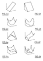
Ces déformées de base sont par exemple du type de celles illustrées sur les figures 4a à 4h : basculement autour d'un côté (figures 4a et 4b), courbure (figure 4c), astigmatisme à O° ou 45° (figures 4d et 4e), déformée de type "coma" (figures 4f et 4g), aberration sphérique (figure 4h).These basic deformations are for example of the type of those illustrated in Figures 4a to 4h: tilting around one side (figures 4a and 4b), curvature (figure 4c), astigmatism at 0 ° or 45 ° (Figures 4d and 4e), deformed type "coma" (Figures 4f and 4g), aberration spherical (Figure 4h).
A titre d'exemple, dans le cas d'un miroir de
forme carrée, un réseau d'électrodes optimisé est du type
de celui représenté sur la figure 5 : il comporte une
électrode 9 centrale de forme carrée, entourée de douze
électrodes périphériques 10, également de forme carrée,
dont la longueur de côté est égale à la demi-longueur de
côté de l'électrode centrale 9.For example, in the case of a mirror
square shape, an optimized electrode network is of the type
that shown in FIG. 5: it includes a
Par ailleurs, du fait de la faible tension
mécanique des membranes de silicium ((45N/m) par rapport
à celle des membranes en nitrure de silicium (520 N/m)),
les tensions de commande appliquées entre l'électrode 2b
et le réseau d'électrodes 3b sont très sensiblement
diminuées par rapport à celles nécessaires pour les
composants à base de nitrure de silicium. Des tensions de
100 V sont suffisantes pour obtenir des déformées de
quelques micromètres, à comparer à des tensions de 250 V
pour les composants à base de nitrure de silicium.Furthermore, due to the low voltage
mechanics of silicon membranes ((45N / m) compared
to that of silicon nitride membranes (520 N / m)),
the control voltages applied between the
Outre l'avantage de simplifier la commande électrique, les membranes silicium permettent d'envisager des déformées de plus grandes amplitudes pour des applications plus contraignantes. Il est en effet envisageable, en appliquant des tensions de commande comparables à celles utilisées avec des membranes en nitrure de silicium (250 V) d'obtenir des déformées ayant des amplitudes supérieures (> 10 µm).Besides the advantage of simplifying the order electric, silicon membranes allow to consider deformations of greater amplitudes for more restrictive applications. It is indeed possible, by applying control voltages comparable to those used with membranes in silicon nitride (250 V) to obtain deformed shapes having higher amplitudes (> 10 µm).
Les composants qui viennent d'être décrits peuvent avantageusement être complétés de la façon suivante.The components which have just been described can advantageously be completed in the way next.
Pour réduire les interférences parasites entre la
surface réfléchissante de la métallisation 5 et
l'électrode transparente 2b en ITO, ladite électrode 2b
est avantageusement recouverte par une couche anti-reflet.To reduce spurious interference between the
reflective surface of
Par ailleurs, il peut être avantageusement prévu
dans le procédé de réalisation une étape consistant à
graver un soufflet à la périphérie de la membrane 1.Furthermore, it can advantageously be provided
in the production process, a step consisting of
engrave a bellows on the periphery of the
En effet, si l'utilisation d'une membrane de silicium fine tendue (d'une épaisseur de l'ordre de 3µm) offre, entre autres, l'avantage de contraintes mécaniques faibles, la périphérie de la membrane est rigidifiée par la structure qui la supporte. Un soufflet de forme générale circulaire permet de réduire cette rigidité.Indeed, if the use of a membrane of fine tensile silicon (with a thickness of the order of 3 μm) offers, among other things, the advantage of mechanical constraints weak, the periphery of the membrane is stiffened by the structure that supports it. A shaped bellows general circular reduces this rigidity.
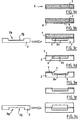
Ainsi que l'illustre les figures 6a à 6c, cette
gravure d'un soufflet est par exemple réalisée avant
l'étape de dopage et de dépôt de métallisation sur la
tranche de SOI. Le soufflet est par exemple constitué par
un ou plusieurs sillons circulaires 11 gravés sur une
épaisseur de silicium de 20 µm.As illustrated in Figures 6a to 6c, this
etching of a bellows is for example carried out before
the doping and metallization deposition step on the
slice of SELF. The bellows is for example constituted by
one or more
En variante encore, les électrodes du réseau 3b
peuvent être remplacées par une électrode unique
commandée optiquement.In another variant, the electrodes of the
Une telle solution permet en effet de simplifier de façon encore accrue l'électronique de commande ; elle permet en outre d'avoir accès à des déformées plus complexes.Such a solution makes it possible to simplify further increased the control electronics; she also allows access to more deformed complex.
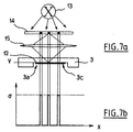
Cette solution optique est illustrée sur les figures 7a et 7b.This optical solution is illustrated on the Figures 7a and 7b.
L'électrode unique (d'ITO par exemple) -
référencée par 3c - est déposée dans le fond de
l'évidement 3a de la lame 3, sur une couche de matériau
photo-conducteur 12 à laquelle elle est ainsi couplée.The single electrode (from ITO for example) -
referenced by 3c - is deposited in the bottom of
the
Une source lumineuse 13, par exemple une lampe
incandescente, éclaire un masque 14 à travers un
diffuseur. Ce masque 14 est représentatif de la
répartition et la forme du champ électrostatique que l'on
désire créer sur la membrane en silicium. L'image de ce
masque est projetée par une lentille 15 sur la lame 3 en
verre supportant l'électrode 3c.A
Le photoconducteur peut être une couche minérale (par exemple un oxyde de bismuth de silicium Bi12 SiO20) ou une couche organique (par exemple du polyvinyl carbozole PVK).The photoconductor can be a mineral layer (for example a silicon bismuth oxide Bi12 SiO20) or an organic layer (for example polyvinyl carbozole PVK).
Le couple électrode-photoconducteur fonctionne de la façon suivante :
- en l'absence de lumière : la tension appliquée sur l'électrode en ITO n'est pas influente sur la membrane Si car le photoconducteur est dans un état isolant,
- aux points éclairés, la tension appliquée sur l'électrode en ITO est transmise sur la face externe du photoconducteur car celui-ci devient conducteur. La force électrostatique est ainsi appliquée à la membrane qui se déforme.
- in the absence of light: the voltage applied to the ITO electrode has no influence on the membrane If the photoconductor is in an insulating state,
- at the lit points, the voltage applied to the ITO electrode is transmitted to the external face of the photoconductor because it becomes conductive. The electrostatic force is thus applied to the deforming membrane.
La conductivité spatiale du photoconducteur
s'écrit :
Cette conductivité présente alors une répartition du type de celle illustrée sur la figure 7bThis conductivity then has a distribution of the type illustrated in FIG. 7b
La faible épaisseur (1 µm à quelques micromètres)
de la couche photoconductrice 12 permet de conserver une
excellente résolution spatiale. La répartition spatiale
de la tension électrique est reproduite fidèlement à
partir de la répartition spatiale de l'intensité
lumineuse incidente.Thin thickness (1 µm to a few micrometers)
of the
On notera que si cette électrode commandable optiquement nécessite un système d'adressage optique supplémentaire, qui peut ne pas être accepté pour certaines applications, cette approche peut être utilisée, en option, pour les applications nécessitant la génération de déformées complexes ne pouvant pas être obtenues avec un simple réseau d'électrodes.Note that if this controllable electrode optically requires an optical addressing system additional, which may not be accepted for some applications this approach can be optionally used for applications requiring generation of complex deformities that cannot be obtained with a simple network of electrodes.
Ce concept permet aussi la génération d'un profil continu du champ de forces électrostatiques. Pour cela, il suffit de choisir un masque dont la transparence n'est pas binaire mais à N niveaux de gris. A la limite, la transparence du masque peut être analogique avec une variation continue de son opacité. D'autre part, le masque peut avoir une fonction dynamique de la transparence. Au lieu d'utiliser un masque où la transparence spatiale est figée une fois pour toutes, on peut, pour certaines applications, utiliser un masque dynamique dont la fonction de transfert évolue temporellement.This concept also allows the generation of a profile continuous field of electrostatic forces. For it, just choose a mask whose transparency is not not binary but at N gray levels. Ultimately, the transparency of the mask can be analog with a continuous variation of its opacity. On the other hand, the mask can have a dynamic function of the transparency. Instead of using a mask where the spatial transparency is frozen once and for all, we may, for certain applications, use a mask dynamic whose transfer function evolves temporally.
Cette spécificité peut être mise à profit pour des applications nécessitant la génération de déformées dynamiques reproduisant une séquence dont les fonctions de transfert, spatiale et temporelle, sont enregistrées au préalable.This specificity can be taken advantage of for applications requiring the generation of deformed shapes dynamics reproducing a sequence whose functions transfer, spatial and temporal, are recorded beforehand.
Une autre variante de la commande électrique peut
être envisagée dans le cas où il est nécessaire
d'accroítre le nombre d'électrodes du réseau 3b. Si ce
nombre d'électrodes est élevé, par exemple de l'ordre de
100 ou supérieur, outre la complexité de la commande
électrique, se pose le problème de l'accès aux différents
plots. Ce problème est bien connu en particulier par les
concepteurs d'écrans plats à cristaux liquides pour la
visualisation. L'accès matriciel pour adresser chaque
point de coordonnée X, Y peut utiliser des lignes et des
colonnes, chacune étant alimentée par des tensions :
+V/2, -V/2 ou 0. Mais ce principe, outre le fait qu'il
nécessite un effet de seuil qui n'existe pas dans
l'application aux membranes à déformation
électrostatique, n'est pas compatible avec un grand
nombre d'électrodes. En effet, en absence d'un effet
mémoire, la tension de commande ne peut être appliquée
que sur une ligne à la fois. Dans le cas de la
visualisation, un artifice consiste à multiplexer
temporellement la commande électrique. Ceci n'est pas
trop gênant pour l'observateur, qui intègre
temporellement les images de chaque ligne grâce à la
rémanence rétinienne.Another variant of the electrical control can
be considered in case it is necessary
to increase the number of electrodes of the
Une approche consiste à créer une mémoire locale attachée à chaque point (pixel pour la visualisation, électrode zonale pour le MMA). On peut à cet effet utiliser des matrices de commande du type de celles utilisées dans le domaine des écrans plats et notamment des matrices de commande utilisant la technologie TFT (Thin Film Transistor).One approach is to create local memory attached to each point (pixel for viewing, zonal electrode for MMA). We can for this purpose use command matrices like those used in the field of flat screens and in particular control matrices using TFT technology (Thin Film Transistor).
Claims (19)
Applications Claiming Priority (2)
| Application Number | Priority Date | Filing Date | Title |
|---|---|---|---|
| FR9906709 | 1999-05-27 | ||
| FR9906709A FR2794251B1 (en) | 1999-05-27 | 1999-05-27 | DEFORMABLE MEMBRANE MIRROR |
Publications (2)
| Publication Number | Publication Date |
|---|---|
| EP1055949A1 true EP1055949A1 (en) | 2000-11-29 |
| EP1055949B1 EP1055949B1 (en) | 2005-11-09 |
Family
ID=9546068
Family Applications (1)
| Application Number | Title | Priority Date | Filing Date |
|---|---|---|---|
| EP20000401459 Expired - Lifetime EP1055949B1 (en) | 1999-05-27 | 2000-05-25 | Mirror with deformable membrane |
Country Status (3)
| Country | Link |
|---|---|
| EP (1) | EP1055949B1 (en) |
| DE (1) | DE60023788T2 (en) |
| FR (1) | FR2794251B1 (en) |
Cited By (3)
| Publication number | Priority date | Publication date | Assignee | Title |
|---|---|---|---|---|
| WO2002091060A2 (en) * | 2001-05-10 | 2002-11-14 | Jean-Pierre Lazzari | Light modulating device |
| WO2004038877A2 (en) * | 2002-10-07 | 2004-05-06 | Coherent, Inc. | Tunable optically-pumped semiconductor laser including a polarizing resonator mirror |
| WO2011051755A1 (en) * | 2009-10-30 | 2011-05-05 | Consiglio Nazionale Delle Ricerche | Optically controlled deformable reflective/refractive assembly with photoconductive substrate |
Citations (4)
| Publication number | Priority date | Publication date | Assignee | Title |
|---|---|---|---|---|
| EP0046873A1 (en) * | 1980-09-02 | 1982-03-10 | Texas Instruments Incorporated | Deformable mirror light modulator |
| US5022745A (en) * | 1989-09-07 | 1991-06-11 | Massachusetts Institute Of Technology | Electrostatically deformable single crystal dielectrically coated mirror |
| US5774252A (en) * | 1994-01-07 | 1998-06-30 | Texas Instruments Incorporated | Membrane device with recessed electrodes and method of making |
| US5822110A (en) * | 1994-09-02 | 1998-10-13 | Dabbaj Rad H | Reflective light valve modulator |
-
1999
- 1999-05-27 FR FR9906709A patent/FR2794251B1/en not_active Expired - Fee Related
-
2000
- 2000-05-25 DE DE2000623788 patent/DE60023788T2/en not_active Expired - Fee Related
- 2000-05-25 EP EP20000401459 patent/EP1055949B1/en not_active Expired - Lifetime
Patent Citations (5)
| Publication number | Priority date | Publication date | Assignee | Title |
|---|---|---|---|---|
| EP0046873A1 (en) * | 1980-09-02 | 1982-03-10 | Texas Instruments Incorporated | Deformable mirror light modulator |
| US5022745A (en) * | 1989-09-07 | 1991-06-11 | Massachusetts Institute Of Technology | Electrostatically deformable single crystal dielectrically coated mirror |
| US5774252A (en) * | 1994-01-07 | 1998-06-30 | Texas Instruments Incorporated | Membrane device with recessed electrodes and method of making |
| US5822110A (en) * | 1994-09-02 | 1998-10-13 | Dabbaj Rad H | Reflective light valve modulator |
| US5822110C1 (en) * | 1994-09-02 | 2001-06-26 | Dabbaj Rad Hassan | Reflective light valve modulator |
Cited By (6)
| Publication number | Priority date | Publication date | Assignee | Title |
|---|---|---|---|---|
| WO2002091060A2 (en) * | 2001-05-10 | 2002-11-14 | Jean-Pierre Lazzari | Light modulating device |
| FR2824643A1 (en) * | 2001-05-10 | 2002-11-15 | Jean Pierre Lazzari | LIGHT MODULATION DEVICE |
| WO2002091060A3 (en) * | 2001-05-10 | 2003-04-03 | Jean-Pierre Lazzari | Light modulating device |
| WO2004038877A2 (en) * | 2002-10-07 | 2004-05-06 | Coherent, Inc. | Tunable optically-pumped semiconductor laser including a polarizing resonator mirror |
| WO2004038877A3 (en) * | 2002-10-07 | 2004-07-08 | Coherent Inc | Tunable optically-pumped semiconductor laser including a polarizing resonator mirror |
| WO2011051755A1 (en) * | 2009-10-30 | 2011-05-05 | Consiglio Nazionale Delle Ricerche | Optically controlled deformable reflective/refractive assembly with photoconductive substrate |
Also Published As
| Publication number | Publication date |
|---|---|
| DE60023788D1 (en) | 2005-12-15 |
| EP1055949B1 (en) | 2005-11-09 |
| FR2794251B1 (en) | 2002-08-02 |
| DE60023788T2 (en) | 2006-06-08 |
| FR2794251A1 (en) | 2000-12-01 |
Similar Documents
| Publication | Publication Date | Title |
|---|---|---|
| EP0610185B1 (en) | Optical modulation device having variable-sized cells | |
| EP2548054B1 (en) | Diffractive combiner for a colour head up display | |
| FR2820834A1 (en) | METHOD FOR MANUFACTURING AN OPTICAL MICRO-MIRROR AND MICRO-MIRROR OR MICRO-MIRROR MATRIX OBTAINED BY THIS PROCESS | |
| EP3239671B1 (en) | Device for detecting electromagnetic radiation with encapsulation structure comprising at least one interference filter | |
| FR2989518A1 (en) | Method for manufacturing integrated image sensor, involves forming pixels at end of columns, and deforming structure such that another end of each of columns is brought closer or separated to form surface in shape of polyhedral cap | |
| WO2015091836A1 (en) | Optical device for stabilising images | |
| WO2012004213A1 (en) | Wave front analyzer having liquid-crystal microlenses | |
| EP1055949B1 (en) | Mirror with deformable membrane | |
| CA2584239C (en) | Deformable mirror | |
| FR2820833A1 (en) | PIVOT OPTICAL MICRO-MIRROR, MATRIX OF SUCH MICRO-MIRRORS AND METHOD FOR PRODUCING SAID MICRO-MIRROR | |
| EP0742459A1 (en) | Optomechanical microdeflector using the displacement of microlenses | |
| EP1008892A1 (en) | Semiconductor phase modulator | |
| EP3123212B1 (en) | Optical device with a deformable membrane | |
| WO2021170708A1 (en) | Multiple resolution display screen and method for producing same | |
| WO2005069057A1 (en) | Optical components and production therof | |
| WO2021228744A1 (en) | Screen for displaying a projected image comprising a structured coating | |
| EP1275020A1 (en) | Optical switch with mobile components and method for making same | |
| EP3764148A1 (en) | Optical network scanner with mobile phase control | |
| WO2021165608A1 (en) | Optical component with encapsulated metasurface and method for manufacturing such a component | |
| EP4070139A1 (en) | Adaptive optical system with improved response time, related use and method | |
| FR2702851A1 (en) | Light modulator based on ferroelectric liquid crystals and having optical addressing | |
| EP1042813A1 (en) | Device comprising a semiconductor chip with insulating and transparent original substrate | |
| FR2835062A1 (en) | MICRO-MIRROR OPTICAL SWITCH AND ITS MANUFACTURING METHOD | |
| EP1097398A1 (en) | Display device with low energy consumption | |
| FR2742224A1 (en) | Silicon@ sensor with controlled membrane thickness |
Legal Events
| Date | Code | Title | Description |
|---|---|---|---|
| PUAI | Public reference made under article 153(3) epc to a published international application that has entered the european phase |
Free format text: ORIGINAL CODE: 0009012 |
|
| AK | Designated contracting states |
Kind code of ref document: A1 Designated state(s): DE FR GB IT |
|
| AX | Request for extension of the european patent |
Free format text: AL;LT;LV;MK;RO;SI |
|
| 17P | Request for examination filed |
Effective date: 20010514 |
|
| AKX | Designation fees paid |
Free format text: DE FR GB IT |
|
| 17Q | First examination report despatched |
Effective date: 20040422 |
|
| GRAP | Despatch of communication of intention to grant a patent |
Free format text: ORIGINAL CODE: EPIDOSNIGR1 |
|
| GRAS | Grant fee paid |
Free format text: ORIGINAL CODE: EPIDOSNIGR3 |
|
| GRAA | (expected) grant |
Free format text: ORIGINAL CODE: 0009210 |
|
| RAP1 | Party data changed (applicant data changed or rights of an application transferred) |
Owner name: SAGEM SA |
|
| AK | Designated contracting states |
Kind code of ref document: B1 Designated state(s): DE FR GB IT |
|
| REG | Reference to a national code |
Ref country code: GB Ref legal event code: FG4D Free format text: NOT ENGLISH |
|
| REF | Corresponds to: |
Ref document number: 60023788 Country of ref document: DE Date of ref document: 20051215 Kind code of ref document: P |
|
| GBT | Gb: translation of ep patent filed (gb section 77(6)(a)/1977) |
Effective date: 20060227 |
|
| RAP2 | Party data changed (patent owner data changed or rights of a patent transferred) |
Owner name: SAGEM DEFENSE SECURITE |
|
| PLBE | No opposition filed within time limit |
Free format text: ORIGINAL CODE: 0009261 |
|
| STAA | Information on the status of an ep patent application or granted ep patent |
Free format text: STATUS: NO OPPOSITION FILED WITHIN TIME LIMIT |
|
| 26N | No opposition filed |
Effective date: 20060810 |
|
| REG | Reference to a national code |
Ref country code: GB Ref legal event code: 732E |
|
| PGFP | Annual fee paid to national office [announced via postgrant information from national office to epo] |
Ref country code: IT Payment date: 20090424 Year of fee payment: 10 Ref country code: DE Payment date: 20090603 Year of fee payment: 10 |
|
| PGFP | Annual fee paid to national office [announced via postgrant information from national office to epo] |
Ref country code: GB Payment date: 20090427 Year of fee payment: 10 |
|
| GBPC | Gb: european patent ceased through non-payment of renewal fee |
Effective date: 20100525 |
|
| PG25 | Lapsed in a contracting state [announced via postgrant information from national office to epo] |
Ref country code: IT Free format text: LAPSE BECAUSE OF NON-PAYMENT OF DUE FEES Effective date: 20100525 |
|
| PG25 | Lapsed in a contracting state [announced via postgrant information from national office to epo] |
Ref country code: DE Free format text: LAPSE BECAUSE OF NON-PAYMENT OF DUE FEES Effective date: 20101201 |
|
| PG25 | Lapsed in a contracting state [announced via postgrant information from national office to epo] |
Ref country code: GB Free format text: LAPSE BECAUSE OF NON-PAYMENT OF DUE FEES Effective date: 20100525 |
|
| PGFP | Annual fee paid to national office [announced via postgrant information from national office to epo] |
Ref country code: FR Payment date: 20120625 Year of fee payment: 13 |
|
| REG | Reference to a national code |
Ref country code: FR Ref legal event code: ST Effective date: 20140131 |
|
| PG25 | Lapsed in a contracting state [announced via postgrant information from national office to epo] |
Ref country code: FR Free format text: LAPSE BECAUSE OF NON-PAYMENT OF DUE FEES Effective date: 20130531 |