BACKGROUND OF THE INVENTION
1. FIELD OF THE INVENTION:
-
The present invention relates to a voltage detecting
circuit for detecting a state of voltage, such as a power
supply voltage detecting circuit.
2. DESCRIPTION OF THE RELATED ART:
-
A power supply voltage detecting circuit is widely
used in various applications, such as detecting the life
of a battery or detecting a capacitor power supply voltage
in a backup mode state. The power supply voltage detecting
circuit is typically incorporated into a micro computer
mainly for portable devices. Moreover, the power supply
voltage detecting circuit can also be used for the generation
of a reset signal for initialization at power-on or
generation of a reset signal for prevention of system runaway
when the power supply voltage changes.
-
A configuration and operation of a conventional
power source voltage detecting circuit 10 will be described
with reference to Figure 1. The power source voltage
detecting circuit 10 includes a detection voltage
generating circuit 11, a reference voltage generating
circuit 12, and a comparison circuit 13. The detection
voltage generating circuit 11 generates a detection
voltage 11a for monitoring a power supply voltage. The
reference voltage generating circuit 12 generates a
reference voltage 12a which is constant and independent of
the power supply voltage. The comparison circuit 13
compares the detection voltage 11a with the reference
voltage 12a and outputs the result of the comparison as a
comparison circuit output signal 13a. A power supply
voltage dividing circuit may, for example, be used as the
detection voltage generating circuit 11. A bandgap
reference circuit may, for example, be used as the reference
voltage generating circuit 12.
-
Figure 2 shows signal levels of a power supply
voltage V. the detection voltage 11a, the reference
voltage 12a, and the comparison circuit output signal 13a
with respect to time. In Figure 2, when the detection
voltage 11a is higher than the reference voltage 12a, the
comparison circuit 13 outputs the comparison circuit output
signal 13a at the same level as the power supply level. The
detection voltage 11a is designed to be proportional to the
power supply voltage V.
-
As is seen from Figure 2, whether the detection
voltage 11a is higher than the reference voltage 12a depends
on the absolute value of variation in the power supply
voltage V. When the detection voltage 11a is higher than
the reference voltage 12a, the output of the comparison
circuit 13 goes to a HIGH level and outputs the comparison
circuit output signal 13a which has the same level as that
of the power supply voltage V. When the detection
voltage 11a is lower than the reference voltage 12a, the
comparison circuit 13 outputs the comparison circuit output
signal 13a having a LOW level. This operation allows
determination if the power supply voltage V has the HIGH
level or the LOW level with respect to a predetermined level.
-
The power source voltage detecting circuit 10
continuously compares the detection voltage 11a with the
reference voltage 12a. The comparison circuit output
signal 13a is continuously output from the comparison
circuit 13. In other words, in the power source voltage
detecting circuit 10, all of the detection voltage
generating circuit 11, the reference voltage generating
circuit 12, and the comparison circuit 13 are continuously
in operation so as to detect the power supply voltage. For
this reason, there is a problem that a power supply current
required to operate these circuits flows continuously.
-
A plausible way to solve such a problem is to
interrupt the power supply current required to operate the
circuits if the comparison circuit 13 outputs the comparison
circuit output signal 13a. However, this is not practical
since the output of the comparison circuit 13 would also
be interrupted. Alternatively, the power supply current
required to operate the circuits may be reduced. In this
case, however, another problem arises such that the circuits
are easily affected by temperature fluctuation and variation
of their elements, thereby reducing the detection accuracy.
SUMMARY OF THE INVENTION
-
According to one aspect of the present invention,
a voltage detecting circuit for detecting a state of a first
voltage, includes a detection voltage generating circuit
for generating a detection voltage depending on the first
voltage; a reference voltage generating circuit for
generating a reference voltage; a comparison circuit for
comparing the detection voltage with the reference voltage
and outputting a result of the comparison as a detection
signal; and a control circuit for controlling at least one
of the detection voltage generating circuit, the reference
voltage generating circuit, and the comparison circuit so
that at least one of these circuits operates intermittently.
-
In one embodiment of this invention, the control
circuit includes an oscillation circuit for outputting a
clock signal.
-
In one embodiment of this invention, the voltage
detecting circuit further includes a frequency dividing
circuit for dividing the clock signal output from the
oscillation circuit by a factor of N, wherein N is a natural
number.
-
In one embodiment of this invention, the circuit
operating intermittently is the comparison circuit.
-
According to another aspect of the present invention,
a voltage detecting method for detecting a state of a first
voltage, includes the step of intermittently comparing a
detection voltage as a monitor of the first voltage with
a reference voltage, and outputting a result of the
comparison as a detection signal.
-
In one embodiment of this invention, a cycle of the
intermittent comparing operation is controlled by a clock
signal having a predetermined frequency.
-
Thus, the invention described herein makes possible
the advantages of providing a voltage detecting circuit and
method having a low power consumption without a decrease
in accuracy of voltage detection.
-
These and other advantages of the present invention
will become apparent to those skilled in the art upon reading
and understanding the following detailed description with
reference to the accompanying figures.
BRIEF DESCRIPTION OF THE DRAWINGS
-
- Figure 1 is a diagram illustrating a configuration
of a conventional power supply voltage detecting circuit.
- Figure 2 is a diagram showing signal levels with
respect to time of a detection voltage 11a, a reference
voltage 12a, a comparison circuit output signal 13a, and
a power supply voltage V.
- Figure 3 is a diagram illustrating a configuration
of a voltage detecting circuit 100 according to Example 1
of this invention.
- Figure 4 is a timing chart showing the output of each
portion of the voltage detecting circuit 100.
- Figure 5 is a diagram illustrating a configuration
of a partially modified version of the voltage detecting
circuit 100.
- Figure 6 is a diagram illustrating a configuration
of a voltage detecting circuit 200 according to Example 2
of this invention.
- Figure 7 is a timing chart showing the output of each
portion of the voltage detecting circuit 200.
- Figure 8 is a table for comparing operational power
supply currents consumed by the voltage detecting
circuit 200 of Example 2 and the conventional voltage
detecting circuit shown in Figure 1.
-
DESCRIPTION OF THE PREFERRED EMBODIMENTS
-
A voltage detecting circuit according to the present
invention includes a detection voltage generating circuit,
a reference voltage generating circuit, and a comparison
circuit. The voltage detecting circuit further includes a
control circuit for controlling at least one of these
circuits so that at least one of these circuits operates
intermittently. The intermittent operation of at least one
of these circuits reduces power consumption by the overall
circuit.
-
The voltage detecting circuit according to the
present invention detects primarily a voltage (hereinafter
referred to as a first voltage). The first voltage may be
a power supply voltage for the voltage detecting circuit
or an integrated circuit carrying the voltage detecting
circuit; or an arbitrary power voltage other than the power
supply voltage (e.g., a power supply voltage of another
integrated circuit or a well bias required for DRAM).
-
The voltage detecting circuit according to the
present invention can be used for the detection of a current
such as a rush current of a heater and a latch-up current
or for the detection of a frequency. To this end, a current
or frequency is converted into a voltage which is in turn
subjected to the voltage detection circuit for detection.
-
Hereinafter, concrete embodiments of the present
invention will be described by way of example using a voltage
detecting circuit for detecting a power supply voltage.
(Example 1)
-
Figure 3 illustrates a configuration of a voltage
detecting circuit 100 of Example 1 for detecting a power
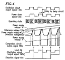
supply voltage. Figure 4 is a timing chart showing the
output of each portion of the voltage detecting circuit 100.
-
The voltage detecting circuit 100 includes a
detection voltage generating circuit 110, a reference
voltage generating circuit 120, and a comparison
circuit 130. The detection voltage generating circuit 110
generates a detection voltage 110a for monitoring a power
supply voltage. The detection voltage 110a has a value
proportional to the value of the power supply voltage (e.g.,
one n-th of the power supply voltage, where n>0). The
reference voltage generating circuit 120 generates a
reference voltage 120a which is constant and independent
of the power supply voltage. The comparison circuit 130
includes a differential comparator. The comparison
circuit 130 compares the detection voltage 110a with the
reference voltage 120a and outputs the result of the
comparison as a comparison circuit output signal 130a. A
power supply voltage dividing circuit may, for example, be
used as the detection voltage generating circuit 110. A
bandgap reference circuit may, for example, be used as the
reference voltage generating circuit 120.
-
In Example 1, the voltage detecting circuit 100
further includes an oscillation circuit 140, a delay
circuit 150, and a latch circuit 160. The oscillation
circuit 140 may include a ring oscillator circuit, for
example.
-
The oscillation circuit 140 outputs a clock signal
(oscillation circuit output signal) 140a having a constant
frequency as shown in Figure 4. The phase of the oscillation
circuit output signal 140a is delayed at a level of about
5 ns±2 ns by the delay circuit 150 and output as a power down
signal 150a as shown in Figure 4. The power down
signal 150a is output from the delay circuit 150. The
detection voltage generating circuit 110, the reference
voltage generating circuit 120, and the comparison
circuit 130 receive the power down signal 150a and operate
intermittently in accordance with the power down signal 150a
to output the detection voltage 110a, the reference
voltage 120a, and the comparison circuit output signal 130a,
as shown in Figure 4.
-
As is seen from Figure 4, in a time period during
which the power down signal 150a has a HIGH level, the
comparison circuit 130 as well as the detection voltage
generating circuit 110 and the reference voltage generating
circuit 120 carry out the comparison operation. In a time
period during which the power down signal 150a has a LOW
level, these circuits are in a power down state so that the
comparison operation is not carried out. As described above,
the detection voltage generating circuit 110, the reference
voltage generating circuit 120, and the comparison
circuit 130 each have a power down function. By the
intermittent comparison operation, the comparison
circuit 130 outputs the comparison circuit output
signal 130a as shown in Figure 4. The voltage detection
circuit 100 has the same comparison operation as that of
the conventional example in the time period during which
the power down signal 150a has the HIGH level.
-
The comparison circuit output signal 130a output
from the comparison circuit 130 is latched by the latch
circuit 160 at the same time of the above-described
intermittent operation. The oscillation circuit output
signal 140a of the oscillation circuit 140 is used as a latch
clock. This latching generates a continuous detection
signal 160a output from the latch circuit 160 as shown in
Figure 4. In Example 1, the delay circuit 150 which
adjusts the timing of latching data is provided so that the
latch circuit 160 can latch securely the comparison circuit
output signal 130a.
-
The detection signal 160a thus obtained can be used
for obtaining information about the power supply voltage
to be detected. Examples of such information include the
life or voltage drop of a battery used as a main power supply
of an information portable device, and the voltage drop of
a capacitor power voltage in a backup mode state (e.g.,
cordless iron). Based on the information, in the case of
a battery in an information portable device, for example,
when the voltage of the battery is lower than a reference
voltage, a part of a circuit inside the information portable
device can be stopped to consume power. The detection
signal 160a may be used as a reset signal for initialization
at power-on or a reset signal for prevention of system
runaway when a power supply voltage changes.
-
In Example 1, assuming that the oscillation circuit
output signal 140a output from the oscillation circuit 140
has a pulse having a duty ratio of 1, the power consumption
by the overall circuit can be reduced in half without
decreasing an operational power supply current of the
circuit itself. Adjustment of the duty ratio of the
oscillation circuit output signal 140a allows optional
variations in the reduction factor of power consumption.
-
In Example 1, the power down signal 150a is supplied
to the detection voltage generating circuit 110, the
reference voltage generating circuit 120, and the
comparison circuit 130 so that all the circuits operate
intermittently. This invention is not limited to this. To
achieve an effect of this invention, i.e., a reduction in
operational power supply current, only one or more of these
circuits may operate intermittently. For example, as shown
in Figure 5, when only the comparison circuit 130 operates
intermittently in the voltage detecting circuit, the delay
circuit 150 is connected neither to the detection voltage
generating circuit 110 nor the reference voltage generating
circuit 120, but only to the comparison circuit 130.
Similarly, connections between the delay circuit 150, and
the detection voltage generating circuit 110 and the
reference voltage generating circuit 120 are optionally
provided so that only the detection voltage generating
circuit 110 and/or the reference voltage generating
circuit 120 may operate intermittently. Such modification
can be applied to Example 2 described later.
-
In Example 1, the oscillation circuit 140 and the
delay circuit 150 constitute a control circuit for
controlling the voltage detecting circuit 100 in such a
manner as to obtain the above-described intermittent
operation. The oscillation circuit 140 (and the delay
circuit 150) generates a pulse signal for obtaining the
intermittent operation. According to this invention, at
least one of the detection voltage generating circuit 110,
the reference voltage generating circuit 120, and the
comparison circuit 130 does not operate continuously but
intermittently. In view of this, another means may be used
as the control circuit instead of the combination of the
oscillation circuit 140 and the delay circuit 150, as long
as it can supply the above-described power down signal and
latch clock signal.
(Example 2)
-
A voltage detecting circuit for detecting a power
supply voltage according to Example 2 of this invention will
be described with reference to Figures 6 and 7. The voltage
detecting device of Example 2 differs from that of Example 1
in that the voltage detecting device of Example 2 is provided
with a frequency dividing circuit for dividing the frequency
of a pulse signal output from an oscillation circuit. Except
for this point, the voltage detecting device of Example 2
has the same structure as that of Example 1.
-
Figure 6 illustrates a configuration of a voltage
detecting circuit 200 of Example 2. Figure 7 is a timing
chart showing the output of each portion of the voltage
detecting circuit 200. The voltage detecting circuit 200
will be described in detail below.
-
The voltage detecting circuit 200 includes a
detection voltage generating circuit 110, a reference
voltage generating circuit 120, and a comparison
circuit 130. The detection voltage generating circuit 110
generates a detection voltage 110a for monitoring a power
supply voltage. The detection voltage 110a has a value
proportional to the value of the power supply voltage (e.g.,
one n-th of the power supply voltage where n>0). The
reference voltage generating circuit 120 generates a
reference voltage 120a which is constant and independent
of the power supply voltage. The comparison circuit 130
includes a differential comparator. The comparison
circuit 130 compares the detection voltage 110a with the
reference voltage 120a and outputs the result of the
comparison as a comparison circuit output signal 130a. A
power supply voltage dividing circuit may, for example, be
used as the detection voltage generating circuit 110. A
bandgap reference circuit may, for example, be used as the
reference voltage generating circuit 120.
-
The voltage detecting circuit 200 further includes
an oscillation circuit 140, a frequency dividing
circuit 142, a delay circuit 150, and a latch circuit 160.
The oscillation circuit 140 may include a ring oscillator
circuit, for example. The oscillation circuit 140 outputs
a clock signal (oscillation circuit output signal) 140a
having a constant frequency as shown in Figure 7, similar
to Example 1.
-
The frequency dividing circuit 142 divides the
frequency of the oscillation circuit output signal 140a
output from the oscillation circuit 140 and outputs a
frequency dividing circuit output signal 142a which is a
clock signal having a specified frequency. A toggle-type
flip-flop (T-FF) circuit may be used as the frequency
dividing circuit 142. The oscillation circuit output
signal 140a and the frequency dividing circuit output
signal 142a are logically synthesized by an AND gate so that
the clock frequency of the oscillation circuit output
signal 140a is divided by a factor of N (N is a natural number)
to obtain a frequency divided signal 140b as shown in
Figure 7. The frequency divided signal 140b is supplied to
the delay circuit 150 and the latch circuit 160.
-
The phase of the frequency divided signal 140b is
delayed at a level of about 5 ns±2 ns by the delay circuit 150
and output as a power down signal 150a as shown in Figure 7.
The power down signal 150a is output from the delay
circuit 150. The detection voltage generating circuit 110,
the reference voltage generating circuit 120, and the
comparison circuit 130 receive the power down signal 150a
and operate intermittently in accordance with the power down
signal 150a to output the detection voltage 110a, the
reference voltage 120a, and the comparison circuit output
signal 130a as shown in Figure 7.
-
As is seen from Figure 7, in a time period during
which the power down signal 150a has a HIGH level, the
comparison circuit 130 as well as the detection voltage
generating circuit 110 and the reference voltage generating
circuit 120 carry out the comparison operation. In a time
period during which the power down signal 150a has a LOW
level, these circuits are in a power down state so that the
comparison operation is not carried out. As described above,
the detection voltage generating circuit 110, the reference
voltage generating circuit 120, and the comparison
circuit 130 each have a power down function. By the
intermittent comparison operation, the comparison
circuit 130 outputs the comparison circuit Output
signal 130a as shown in Figure 7. The voltage detection
circuit 200 has the same comparison operation as that of
the conventional example in the time period during which
the power down signal 150a has the HIGH level.
-
The comparison circuit output signal 130a output
from the comparison circuit 130 is latched by the latch
circuit 160 at the same time of the above-described
intermittent operation. The frequency divided signal is
used as a latch clock. This latching generates a continuous
detection signal 160a output from the latch circuit 160 as
shown in Figure 7. In Example 2, the delay circuit 150
which adjusts the timing of latching data is provided in
order that the latch circuit 160 can latch securely the
comparison circuit output signal 130a.
-
In Example 2, the frequency dividing circuit 142
divides an input signal by a factor of 2, so that power
consumption by the overall circuit can be further reduced
in half as compared with Example 1. Although a frequency
division factor is two in Example 2, the frequency division
factor may be another value (three or more). Power
consumption by the overall circuit can be reduced to the
desired level by setting the frequency division factor N
of the frequency dividing circuit to an appropriate value
(natural number).
-
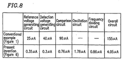
Figure 8 is a table showing data of the operational
power supply current consumed by the voltage detecting
circuit 200 of Example 2 and the conventional voltage
detecting circuit shown in Figure 1. In Figure 8, results
for the voltage detecting circuit 200 of Example 2 are
obtained where the power supply voltage is 5 V and the
frequency division factor of the frequency dividing
circuit 142 is, for example, 150 (the clock frequency of
the oscillation circuit output signal 140a of the
oscillation circuit 140 is divided by a factor of 150), i.e.,
a detecting operation is performed for about 1 µs in each
interval of about 150 µs. As is seen from Figure 8, in the
voltage detecting circuit 200, the overall reduced amount
of operational power supply current of the reference voltage
generating circuit, the detection voltage generating
circuit, and the comparison circuit is greater than the
overall increased amount of operational power supply current
of the oscillation circuit and the frequency dividing
circuit. The frequency dividing circuit 142 having a
frequency division factor of 150 leads to a reduction in
operational power supply current consumed by the overall
circuit to about 2.6 % of that of the conventional example
shown in Figure 1. The frequency division factor of the
frequency dividing circuit 142 may be set to be an
appropriate value depending on the object having the voltage
to be detected.
-
The voltage detecting circuit of this invention
includes the control circuit for controlling the voltage
detecting circuit in such a manner that at least one of the
detection voltage generating circuit, the reference voltage
generating circuit, and the comparison circuit operates
intermittently. The intermittent operation of the circuit
allows a reduction in power consumption by the overall
circuit. According to this invention, low power
consumption is achieved without a reduction in detection
accuracy of the circuit. The use of the voltage detecting
circuit of this invention can increase the life of a power
supply battery as a main battery.
-
Various other modifications will be apparent to and
can be readily made by those skilled in the art without
departing from the scope and spirit of this invention.
Accordingly, it is not intended that the scope of the claims
appended hereto be limited to the description as set forth
herein, but rather that the claims be broadly construed.