EP1035445A2 - Microlithographic reduction objective and projection exposure apparatus - Google Patents
Microlithographic reduction objective and projection exposure apparatus Download PDFInfo
- Publication number
- EP1035445A2 EP1035445A2 EP99125783A EP99125783A EP1035445A2 EP 1035445 A2 EP1035445 A2 EP 1035445A2 EP 99125783 A EP99125783 A EP 99125783A EP 99125783 A EP99125783 A EP 99125783A EP 1035445 A2 EP1035445 A2 EP 1035445A2
- Authority
- EP
- European Patent Office
- Prior art keywords
- mirror
- microlithography projection
- projection lens
- lens device
- mirrors
- Prior art date
- Legal status (The legal status is an assumption and is not a legal conclusion. Google has not performed a legal analysis and makes no representation as to the accuracy of the status listed.)
- Granted
Links
Images


Classifications
-
- G—PHYSICS
- G03—PHOTOGRAPHY; CINEMATOGRAPHY; ANALOGOUS TECHNIQUES USING WAVES OTHER THAN OPTICAL WAVES; ELECTROGRAPHY; HOLOGRAPHY
- G03F—PHOTOMECHANICAL PRODUCTION OF TEXTURED OR PATTERNED SURFACES, e.g. FOR PRINTING, FOR PROCESSING OF SEMICONDUCTOR DEVICES; MATERIALS THEREFOR; ORIGINALS THEREFOR; APPARATUS SPECIALLY ADAPTED THEREFOR
- G03F7/00—Photomechanical, e.g. photolithographic, production of textured or patterned surfaces, e.g. printing surfaces; Materials therefor, e.g. comprising photoresists; Apparatus specially adapted therefor
- G03F7/70—Microphotolithographic exposure; Apparatus therefor
- G03F7/70216—Mask projection systems
- G03F7/70233—Optical aspects of catoptric systems, i.e. comprising only reflective elements, e.g. extreme ultraviolet [EUV] projection systems
-
- G—PHYSICS
- G02—OPTICS
- G02B—OPTICAL ELEMENTS, SYSTEMS OR APPARATUS
- G02B17/00—Systems with reflecting surfaces, with or without refracting elements
- G02B17/02—Catoptric systems, e.g. image erecting and reversing system
- G02B17/06—Catoptric systems, e.g. image erecting and reversing system using mirrors only, i.e. having only one curved mirror
- G02B17/0647—Catoptric systems, e.g. image erecting and reversing system using mirrors only, i.e. having only one curved mirror using more than three curved mirrors
- G02B17/0657—Catoptric systems, e.g. image erecting and reversing system using mirrors only, i.e. having only one curved mirror using more than three curved mirrors off-axis or unobscured systems in which all of the mirrors share a common axis of rotational symmetry
-
- G—PHYSICS
- G03—PHOTOGRAPHY; CINEMATOGRAPHY; ANALOGOUS TECHNIQUES USING WAVES OTHER THAN OPTICAL WAVES; ELECTROGRAPHY; HOLOGRAPHY
- G03F—PHOTOMECHANICAL PRODUCTION OF TEXTURED OR PATTERNED SURFACES, e.g. FOR PRINTING, FOR PROCESSING OF SEMICONDUCTOR DEVICES; MATERIALS THEREFOR; ORIGINALS THEREFOR; APPARATUS SPECIALLY ADAPTED THEREFOR
- G03F7/00—Photomechanical, e.g. photolithographic, production of textured or patterned surfaces, e.g. printing surfaces; Materials therefor, e.g. comprising photoresists; Apparatus specially adapted therefor
- G03F7/70—Microphotolithographic exposure; Apparatus therefor
- G03F7/70216—Mask projection systems
- G03F7/7025—Size or form of projection system aperture, e.g. aperture stops, diaphragms or pupil obscuration; Control thereof
-
- G—PHYSICS
- G03—PHOTOGRAPHY; CINEMATOGRAPHY; ANALOGOUS TECHNIQUES USING WAVES OTHER THAN OPTICAL WAVES; ELECTROGRAPHY; HOLOGRAPHY
- G03F—PHOTOMECHANICAL PRODUCTION OF TEXTURED OR PATTERNED SURFACES, e.g. FOR PRINTING, FOR PROCESSING OF SEMICONDUCTOR DEVICES; MATERIALS THEREFOR; ORIGINALS THEREFOR; APPARATUS SPECIALLY ADAPTED THEREFOR
- G03F7/00—Photomechanical, e.g. photolithographic, production of textured or patterned surfaces, e.g. printing surfaces; Materials therefor, e.g. comprising photoresists; Apparatus specially adapted therefor
- G03F7/70—Microphotolithographic exposure; Apparatus therefor
- G03F7/70216—Mask projection systems
- G03F7/70275—Multiple projection paths, e.g. array of projection systems, microlens projection systems or tandem projection systems
Definitions
- the invention relates to a microlithography lens according to the preamble of claim 1, a projection exposure apparatus according to claim 29 and a chip manufacturing method according to claim 32.
- Optical systems are used for imaging systems in the EUV area essentially reflective systems with multilayer layers are available.
- the reflectivity of the multilayer layers used is only in the range of is about 70%, it is the projection lenses for EUV microlithography vital to achieve one sufficient light intensity with as few optical components as possible EUV projection lens get along.
- 6-mirror systems for microlithography are from the publications US-A-5686728 and EP 0779528 and US 5815310 have become known.
- the projection lithography system according to US-A-5686728 shows a Projection lens with six mirrors, each of the reflective Mirror surfaces is aspherical. The mirrors are along one common optical axis arranged so that an obscuration-free Light path is reached.
- EP-A-0779528 describes a projection objective with six mirrors Use in EUV lithography, especially at wavelengths of 13 nm and 11 nm.
- This projection lens also has the disadvantage that at least two of the a total of six mirrors very high asphericities of 26 and 18.5 ⁇ m exhibit.
- EP-A-0779528 known arrangement of the optical free working distance between wafnext mirrors and wafers so low that it either too Instabilities or a mechanically free working distance that is negative is coming.
- the object of the invention is therefore one for lithography with short Wavelengths, preferably less than 100 nm, are suitable Projection lens device specify the disadvantages mentioned above of the prior art.
- the object is thereby achieved in a first embodiment solved that with a projection lens with six mirrors waferssene mirror is arranged such that the image-side numerical Aperture is greater than or equal to 0.15 and the wafer-side optical free Working distance at least the used diameter of the next wafer Corresponds to the mirror and / or the wafer-side optical free working distance at least the sum of one third of the diameter used Mirror and a length that is between 20 and 30 mm, and / or the optical free working distance on the wafer side is at least 50 mm, is preferably 60 mm.
- the object-side numerical aperture NA is greater than 0.15
- the ring field width W on the wafer is in the range 1.0 mm ⁇ W
- the tip-to-tip deviation A of the aspheres is through on all mirrors compared to the best-fitting sphere in the useful area A ⁇ 19 ⁇ m - 102 ⁇ m (0.25- N / A ) - 0.7 ⁇ m mm (2nd mm - W ) limited.
- the tip-tip deviation A of the aspheres is particularly preferred on all mirrors A ⁇ 12 ⁇ m - 64 ⁇ m (0.25- N / A ) - 0.3 ⁇ m mm (2nd mm - W ) limited.
- the angles of incidence AOI relative to the surface normal of all rays are through on all mirrors AOI ⁇ 23 ° - 35 ° (0.25 - N / A ) - 0.2 ° / mm (2nd mm- W ) limited.
- the asphericities discussed in this document refer to the tip-tip or peak to valley (PV) deviation A of the aspherical surfaces compared to the best-fitting sphere in the usable area.
- PV peak to valley
- the information on the angles of incidence relate to the angle between the respective incident beam and surface normal at the point of incidence.
- the largest angle of any ray is given, in general a beam-limiting beam that appears at any of the mirrors.
- the optical free working distance is particularly preferably 60 mm.
- the lenses described above can not only be used in the EUV , but of course also at other wavelengths, without deviated from the invention.
- the Mirrors of the projection lens are arranged such that the Lighting is free from obscuration.
- the projection lens device as a system with Intermediate image is executed. It is particularly preferred if that Intermediate image is formed after the fourth mirror. With such Constructions it is possible that the aperture in the front, low-aperture Lens part comes to lie and a conjugated pupil plane in the Focus of the last mirror is mapped. Such a structure poses a telecentric beam path in the image space.
- the free accessible aperture optically and physically between the second and third Mirror is arranged.
- the aperture is easily accessible if the distance from the first and third mirrors to the first and second mirrors in the area 0.5 ⁇ S1S3 S1S2 ⁇ 2 lies.
- the angular loads in the front part of the projection lens can also be reduced by means of an elongated structure, as implemented in the first embodiment of the invention.
- a diaphragm physically between S2 and S1 must at least partially formed as a narrow ring to cut the Avoid S1 after S2 running bundle. With such a Design there is a risk that undesirable direct or at S1 and S2 reflected light passes the aperture outside of this ring and reached the wafer.
- the aperture can both as an opening in the first mirror or behind the first mirror be carried out.
- the aperture is provided or to be placed close to the second mirror.
- An arrangement of the aperture the mirror has the advantage that it is mechanically simple to implement.
- a manufacturing simplification is achieved if in one alternative embodiment is provided, a maximum of five mirrors to train aspherically. It is then possible to use a mirror, preferably the largest mirror, here in the form of the quaternary mirror, spherical to train.
- An arrangement of the second to sixth mirror is particularly preferred in the order concave - convex - concave - convex - concave.
- the design portion of the system's rms wavefront portion is at most 0.07 ⁇ , preferably 0.03 ⁇ .
- the lenses are always in the examples of the invention telecentric on the image side.
- the Projection lens is designed telecentrically on the object side.
- the first mirror is preferably concave.
- the telecentricity error on the wafer should not be 10 mrad exceed, preferably it is 5 mrad, particularly preferably 2 mrad. This ensures that the change in the magnification holds within tolerable limits over the depth of field.
- this one Field mirror, a scaling down three-mirror subsystem and a two-mirror subsystem includes.
- the Invention also a projection exposure system, comprising at least such a facility.
- the projection exposure system has a reflection mask, in a alternative embodiment, a transmission mask.
- the projection exposure system has a Illumination device for illuminating an off-axis ring field includes and the system is designed as a ring field scanner. It is an advantage provided that the secant length of the scan slot is at least 26 mm is and the ring width is greater than 0.5 mm, so that a homogeneous Lighting is enabled.
- FIG. 2 shows a system according to the prior art for Wavelengths> 100 nm, as known for example from US-A-5686728.
- the aberrations of the subsystems are balanced against each other that the overall system is of sufficient quality for the application.
- the physical aperture B is between the second mirror S2 and the third Mirror S3 arranged. As is clear from Figure 1, the aperture is accessible in the beam path between the second mirror S2 and the third Mirror S3.
- the optical working distance between the next mirror next to the wafer, that is the fifth mirror S5 in the present exemplary embodiment, and the wafer plane 4 is larger than the diameter of the mirror S5 used, ie the following condition is met: optical distance S5 to wafer level 4> used diameter S5.
- optical working distance is greater than the sum of one third of the used diameter of the next mirror S5 plus 20 mm or is more than 50 mm.
- the free optical working distance is 60 mm without being limited to this.
- Such an optical working distance guarantees a sufficiently free one mechanical working distance that is greater than 0 and the use of optical components with sufficient strength properties for Wavelengths ⁇ 100 nm, preferably 11 or 13 nm.
- the reflectivities of the systems are achievable in the range of approximately 70%.
- the multilayer coating systems can Layer stresses of 350 MPa and more occur that Surface deformation, especially in the edge areas of the mirrors induce.
- the beam path of the objective shown in FIG. 1 is free of obscuration.
- the projection objectives according to the invention are preferably used in ring field scan projection exposure systems, the secant length of the scan slot being at least 26 mm.
- the telecentric system on the image side can be telecentric on the object side or not be telecentric, being a telecentric Beam path on the object side only when using a reflection lens
- Use of a transmission-reducing beam splitter is possible.
- Unevenness of the mask result in a non-telecentric beam path in the Object space for scale errors in the figure.
- the main beam angles on Reticles are therefore preferably below 10 °, so that the requirements for Flatness of the reticle lies in the range of technologically feasible.
- the system according to the invention according to FIG. 1 has an image side Telecentricity error on the wafer of 1 mrad with a numerical aperture of 0.2 on.
- the entrance pupil of the last one is located Mirror S6 at or near its focal point.
- the aperture comes in the front, low-aperture lens part mainly between the first and third Mirrors S1, S3 for lying and the pupil plane conjugated to it is shown in the focus of the last mirror.
- all mirrors are S1-S6 made aspherical, the maximum asphericity in the useful area at 7.3 ⁇ m.
- the low asphericity of the arrangement according to the invention is Particularly advantageous from a manufacturing point of view, since the technological difficulties in machining the surfaces of the Multilayer mirror with the aspherical deviation and growing Gradients of the asphere increase disproportionately.
- the large angle of incidence in the arrangement according to FIG. 1 occurs at S5 and is 18.4 °.
- the maximum angle of incidence of mirror occurs at mirror S5 about 14.7 ° above the mirror.
- the aperture arranged between the second and third mirrors in the embodiment according to FIG. 1 is freely accessible.
- a free accessibility of the aperture and a shading of the bundle running from S3 to S4 through the aperture is prevented with at the same time acceptable angles of incidence on the mirrors, if in the arrangements shown, the following condition 0.5 ⁇ S1S3 S1S2 ⁇ 2 and 0.5 ⁇ S2 aperture S3 aperture ⁇ 2 are fulfilled.
- the short form S1S3 denotes the mechanical distance between the individual components, here mirrors S1 and S3.
- the distance from the reticle to S1 is smaller than the distance from S2 to S3, ie the following applies: Reticle S1 ⁇ S2S3.
- the distance between reticle S2 is 80 mm, without being restricted to this his.
- the distance between the mirrors S3 and S6 so large chosen that the mirror can be made sufficiently thick to in the case of the high layer tensions that occur above the required To have strength properties.
- the following table shows in Code V nomenclature the parameters of the systems shown by way of example in FIG. 1.
- the lens is a 5x system with a 26 x 2 mm 2 ring field and a numerical aperture of 0.2.
- the mean image-side radius of the system is approximately 26 mm.
- FIG. 2 shows an arrangement of a projection lens for the Microlithography with wavelength ⁇ ⁇ 100 nm according to US-A-5686728 shown.
- the same components as in Figure 1 are given the same reference numerals busy.
- the distance between the next wafer Mirror S5 and the wafer much smaller than the diameter of the Mirror and in the present case is in the range of approximately 20 mm, which is in the EUV range due to the extreme layer stresses to strength problems leads.
- the system according to the prior art has very high Asphericities of +/- 50 ⁇ m and angle of incidence of 38 °.
- Such Asphericities and angles of incidence are in the EUV range from the perspective manufacturing and coating technology not feasible.
- Figure 3 is an alternative embodiment of an inventive 6-mirror system shown, in which the aperture on the first mirror lies.
- the same components as in Figure 1 are again the same Reference numbers occupied.
- the optical free working distance on the wafer is also this Embodiment as in the embodiment according to FIG. 1 60 mm and is therefore larger than the diameter of the mirror S5 next to the wafer.
- the design according to FIG Figure 3 shows the distance between S2 and S3 compared to the prior art in the form of US-A-5686728 has been increased significantly so that large Incidence angles in the system can be reduced.
- the diaphragm is in FIG. 3 B physically placed on the primary mirror.
- S2 the diaphragm
- the embodiment shown in FIG. 3 can either be an opening in the S1 mother mirror or behind S1.
- Another advantage of the solution according to FIG. 3 is the spherical design of the mirror S4, which represents a particular advantage in particular from a manufacturing perspective, since the mirror S4 is the largest mirror in the system.
- the asphericity in the useful area is slightly increased in the embodiment according to FIG. 3 and is 10.5 ⁇ m.
- the greatest angle of incidence occurs at mirror S5 and is approximately 18.6 °.
- Table 2 shows the construction data of the 5x objective according to FIG. 3 in code V nomenclature, the fourth mirror S4 being spherical.
- the average radius of the 26 x 1.7 mm 2 image field is again 26 mm.
- the aperture B was optically and physically placed on the secondary mirror or second mirror S2.
- the arrangement of the diaphragm directly on the mirror has the advantage that this Aperture on a mirror is easier to implement mechanically.
- the optical free working distance between the wafer and wafer next mirror S5 larger than the diameter of the invention next to the mirror S5 and in the present embodiment is approx. 59 mm.
- Table 3 lists the optical parameters in Code V nomenclature of the embodiment of the invention shown in FIG.
- FIG. 5 shows an embodiment of the invention, which has a field mirror S1, a first subsystem with second to fourth mirrors S2 - S4 and a second Subsystem with fifth and sixth mirrors S5, S6 comprises.
- the field mirror S1 with ⁇ > 0 generates a virtual image of the object 2, which is characterized by the first formed from second, third and fourth mirrors S2, S3, S4 Subsystem with ⁇ ⁇ 0 is mapped real into the intermediate image Z, the the second subsystem formed from the fifth and sixth mirrors S5, S6 Maps intermediate image Z into the real system image of wafer level 4.
- the working distance between the last mirror S5 and the wafer level corresponds at least to that Sum of one third of the diameter used next to the wafer Mirror and a length that is between 20 and 30 mm. Aperture B comes to rest on the second mirror S2.
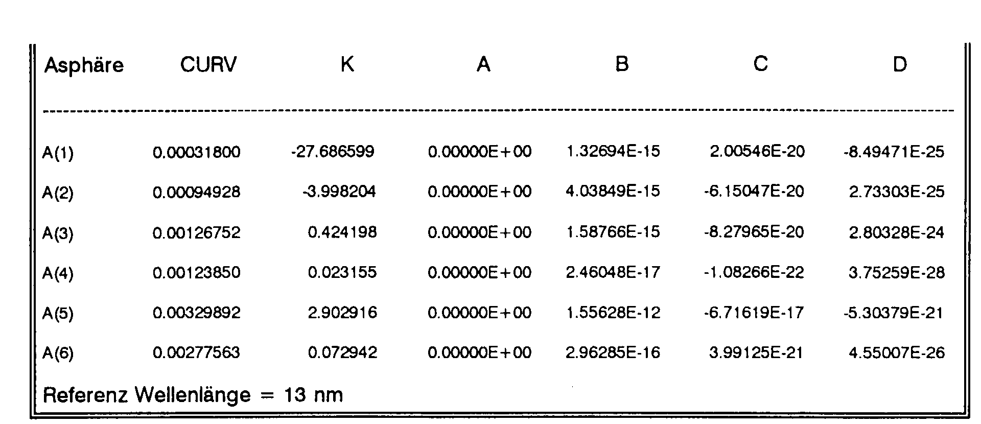
- Table 4 lists the optical parameters of the embodiment according to FIG. 5 in code V nomenclature.
- FIG. 6 shows a second embodiment of a 6-mirror lens Field mirror S1, first and second subsystem and intermediate image Z shown.
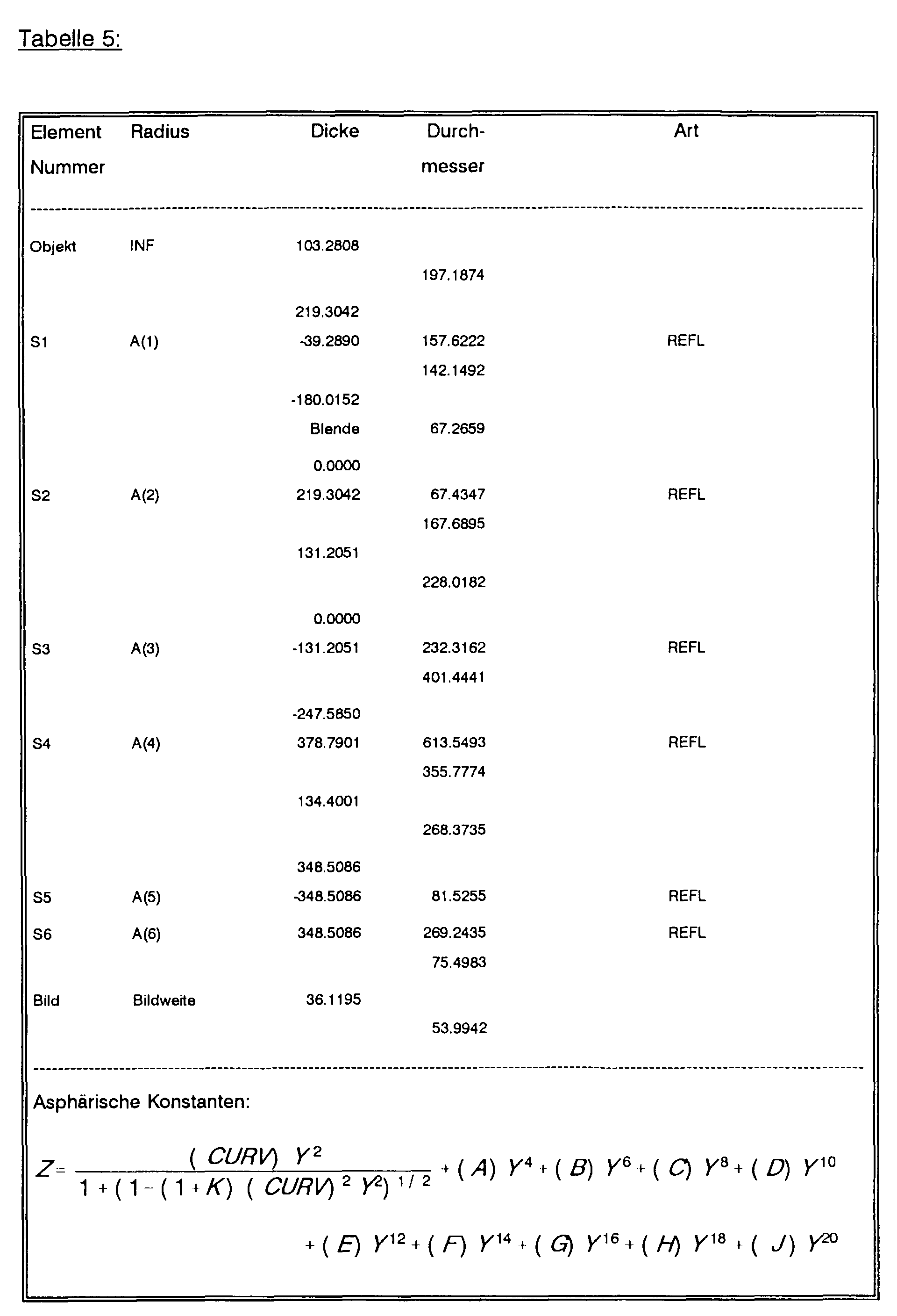
- optical parameters of the embodiment according to FIG. 6 are listed in Table 5 in Code V nomenclature.
- FIGS. 7A and 7B again illustrate what is in the present Registration is to be understood under the diameter D used.
- the illuminated field 100 on a mirror in FIG. 7A is an example a rectangular field.
- the diameter D used is then the diameter of the enveloping circle 102 which encloses the rectangle 100, the corners 104 of the rectangle 100 come to lie on the enveloping circle 102.
- FIG. 7B A second example is shown in FIG. 7B.
- the illuminated field 100 has a kidney shape, as for the useful area when using the Lenses according to the invention in a microlithography projection exposure system expected.
- the enveloping circle 102 encloses the Kidney shape completely and falls at two points 106, 108 with the edge 110 of the Kidney shape together.
- the diameter D used then results from the diameter of the enveloping circle 102.
- a 6-mirror projection lens is thus used for the first time a magnification of preferably 4x, 5x and 6x for the preferred use in an EUV ring field projection system specified that both the necessary resolution for the required image field as well Design conditions, which has a functional Construction allows the angles because the aspheres are sufficiently mild sufficiently small for the layers and the installation space for the mirror supports are sufficiently large.
Abstract
Die Erfindung betrifft eine Mikrolithographie-Projektionsobjektiveinrichtung für kurze Wellenlängen, vorzugsweise < 100 nm mit einem ersten (S1), einem zweiten Spiegel (S2), einem dritten (S3), einem vierten Spiegel (S4), einem fünften (S5) und einem sechsten Spiegel (S6). Die Erfindung ist dadurch gekennzeichnet, daß die bildseitige numerische Apertur NA >= 0,15 ist und der dem zu belichtenden Objekt vorzugsweise dem Wafer am nächsten kommende Spiegel derart angeordnet ist, daß der bildseitige optische freie Arbeitsabstand mindestens dem genutzten Durchmesser D dieses wafernächsten Spiegels entspricht und/oder der bildseitige optische freie Arbeitsabstand mindestens die Summe aus einem Drittel des genutzten Durchmessers D dieses Spiegels und einer Länge, die zwischen 20 mm und 30 mm liegt, beträgt und/oder der bildseitseitige optische freie Arbeitsabstand mindestens 50 mm, vorzugsweise 60 mm beträgt. <IMAGE>The invention relates to a microlithography projection lens device for short wavelengths, preferably <100 nm, with a first (S1), a second mirror (S2), a third (S3), a fourth mirror (S4), a fifth (S5) and a sixth Mirror (S6). The invention is characterized in that the image-side numerical aperture NA> = 0.15 and the mirror closest to the object to be exposed is preferably arranged in such a way that the image-side optical free working distance corresponds at least to the diameter D used of this mirror next to the wafer and / or the optical free working distance on the image side is at least the sum of one third of the used diameter D of this mirror and a length which is between 20 mm and 30 mm, and / or the optical free working distance on the image side is at least 50 mm, preferably 60 mm . <IMAGE>
Description
Die Erfindung betrifft ein Mikrolithographieobjektiv gemäß dem Oberbegriff
von Anspruch 1, eine Projektionsbelichtungsanlage gemäß Anspruch 29 sowie
ein Chipherstellungsverfahren gemäß Anspruch 32.The invention relates to a microlithography lens according to the preamble
of
Die Lithographie mit Wellenlängen < 193 nm, insbesondere die EUV-Lithographie
mit λ = 11 nm bzw. λ = 13 nm werden als mögliche Techniken
zur Abbildungen von Strukturen < 130 nm, besonders bevorzugt < 100 nm
diskutiert. Die Auflösung eines lithographischen Systems wird durch
nachfolgende Gleichung beschrieben:
Für abbildende Systeme im EUV-Bereich stehen als optische Komponenten im wesentlichen reflektive Systeme mit Multilayer-Schichten zur Verfügung. Als Multilayer-Schichtsysteme finden bei λ = 11 nm bevorzugt Mo/Be-Systeme und bei λ = 13 nm Mo/Si-Systeme Verwendung.Optical systems are used for imaging systems in the EUV area essentially reflective systems with multilayer layers are available. As Multilayer coating systems prefer Mo / Be systems at λ = 11 nm and at λ = 13 nm Mo / Si systems use.
Legt man eine eine numerische Apertur von 0,2 zugrunde, so erfordert die Abbildung von 50 nm-Strukturen mit 13 nm-Strahlung einen vergleichsweise einfachen Prozeß mit k1 = 0,77. Mit k1 = 0,64 wird bei 11 nm-Strahlung die Abbildung von 35 nm-Strukturen möglich. Assuming a numerical aperture of 0.2, the imaging of 50 nm structures with 13 nm radiation requires a comparatively simple process with k 1 = 0.77. With k 1 = 0.64, the imaging of 35 nm structures is possible with 11 nm radiation.
Da die Reflektivität der eingesetzten Multilayer-Schichten nur im Bereich von ungefähr 70 % liegt, ist es bei den Projektionsobjektiven für die EUV-Mikrolithographie von ganz entscheidender Bedeutung, zum Erreichen einer ausreichenden Lichtstärke mit möglichst wenig optischen Komponenten im EUV-Projektionsobjektiv auszukommen.Since the reflectivity of the multilayer layers used is only in the range of is about 70%, it is the projection lenses for EUV microlithography vital to achieve one sufficient light intensity with as few optical components as possible EUV projection lens get along.
Als besonders bevorzugt haben sich mit Blick auf eine hohe Lichtintensität und ausreichende Möglichkeiten zur Korrektur von Abbildungsfehlern bei NA = 0,20 Systeme mit sechs Spiegeln herausgestellt.Have been particularly preferred with a view to a high light intensity and sufficient possibilities to correct aberrations NA = 0.20 systems with six mirrors highlighted.
6-Spiegel-Systeme für die Mikrolithographie sind aus den Druckschriften US-A-5686728 und EP 0779528 bzw. US 5815310 bekannt geworden.6-mirror systems for microlithography are from the publications US-A-5686728 and EP 0779528 and US 5815310 have become known.
Das Projektions-Lithographiesystem gemäß der US-A-5686728 zeigt ein Projektionsobjektiv mit sechs Spiegeln, wobei jede der reflektiven Spiegelflächen asphärisch ausgebildet ist. Die Spiegel sind entlang einer gemeinsamen optischen Achse so angeordnet, daß ein obskurationfreier Lichtweg erreicht wird.The projection lithography system according to US-A-5686728 shows a Projection lens with six mirrors, each of the reflective Mirror surfaces is aspherical. The mirrors are along one common optical axis arranged so that an obscuration-free Light path is reached.
Da das aus der US-A-5686728 bekannte Projektionsobjektiv nur für UV-Licht mit einer Wellenlänge von 100 - 300 nm eingesetzt wird, weisen die Spiegel dieses Projektionsobjektives eine sehr hohe Asphärizität von ungefähr +/- 50 µm sowie sehr große Einfallswinkel von ca. 38° auf. Auch nach Abblenden auf NA = 0,2 verbleibt hier eine Asphärizität von 25 µm von Spitze zu Spitze bei kaum vermindertem Einfallswinkel. Derartige Asphärizitäten und Einfallwinkel sind im EUV-Bereich wegen der hohen Anforderungen an die Oberflächenqualität, Reflektivität der Spiegel nach heutigem Stand der Technik nicht praktikabel.Since the projection lens known from US-A-5686728 only for UV light with a wavelength of 100 - 300 nm, the mirrors have this projection lens has a very high asphericity of approximately +/- 50 µm and very large angles of incidence of approx. 38 °. Even after Stopping down to NA = 0.2 leaves an asphericity of 25 µm from the tip to tip with hardly any reduced angle of incidence. Such asphericities and Incidence angles are in the EUV area because of the high demands on the Surface quality, reflectivity of the mirrors according to the current state of the Technology not practical.
Ein weiterer Nachteil des aus der US-A-5686728 bekannt gewordenen Objektives, der einen Einsatz im Bereich von λ < 100 nm, insbesondere bei den Wellenlängen von 11 und 13 nm nicht mehr erlaubt, ist der sehr geringe Abstand zwischen dem Wafer und dem dem Wafer am nächsten liegenden Spiegel. Bei den aus der US-A-5686728 bekanntgewordenen Abständen von Wafer und wäfernächstem Spiegel können die Spiegel nur sehr dünn ausgebildet werden. Wegen der extremen Schicht-Spannungen in den Multilayer-Systemen für die angesprochenen Wellenlängen von 11 und 13 nm sind derartige Spiegel sehr instabil.Another disadvantage of that known from US-A-5686728 Objectives that can be used in the range of λ <100 nm, especially at the wavelengths of 11 and 13 nm are no longer allowed, is the very small one Distance between the wafer and the one closest to the wafer Mirror. At the intervals of known from US-A-5686728 Wafers and the next mirror can only be very thin be formed. Because of the extreme layer tensions in the Multilayer systems for the mentioned wavelengths of 11 and 13 nm such mirrors are very unstable.
Aus der EP-A-0779528 ist ein Projektionsobjektiv mit sechs Spiegeln zum Einsatz in der EUV-Lithographie, insbesondere auch bei Wellenlängen von 13 nm und 11 nm, bekanntgeworden.EP-A-0779528 describes a projection objective with six mirrors Use in EUV lithography, especially at wavelengths of 13 nm and 11 nm.
Auch dieses Projektionsobjektiv hat den Nachteil, daß mindestens zwei der insgesamt sechs Spiegel sehr hohe Asphärizitäten von 26 bzw. 18,5 µm aufweisen. Insbesondere ist aber auch bei der aus der EP-A-0779528 bekannten Anordnung der optische freie Arbeitsabstand zwischen wafernächstem Spiegel und Wafer derart gering, daß es entweder zu Instabilitäten oder aber einem mechanisch freien Arbeitsabstand, der negativ ist, kommt.This projection lens also has the disadvantage that at least two of the a total of six mirrors very high asphericities of 26 and 18.5 µm exhibit. In particular, however, is also that from EP-A-0779528 known arrangement of the optical free working distance between wafnext mirrors and wafers so low that it either too Instabilities or a mechanically free working distance that is negative is coming.
Aufgabe der Erfindung ist es somit, eine für die Lithographie mit kurzen Wellenlängen, vorzugweise kleiner 100 nm, geeignete Projektionsobjektiveinrichtung anzugeben, die die zuvor erwähnten Nachteile des Standes der Technik nicht aufweist.The object of the invention is therefore one for lithography with short Wavelengths, preferably less than 100 nm, are suitable Projection lens device specify the disadvantages mentioned above of the prior art.
Erfindungsgemäß wird die Aufgabe in einer ersten Ausgestaltung dadurch gelöst, daß bei einem Projektionsobjektiv mit sechs Spiegeln der wafernächste Spiegel derart angeordnet ist, daß die bildseitige numerische Apertur größer gleich 0,15 ist und der waferseitige optische freie Arbeitsabstand mindestens dem genutzten Durchmesser des wafernächsten Spiegels entspricht und/oder der waferseitige optische freie Arbeitsabstand mindestens der Summe aus einem Drittel des genutzten Durchmessers dieses Spiegels und einer Länge, die zwischen 20 und 30 mm liegt, beträgt und/oder der waferseitige optische freie Arbeitsabstand mindestens 50 mm, vorzugsweise 60 mm beträgt.According to the invention, the object is thereby achieved in a first embodiment solved that with a projection lens with six mirrors wafernächste mirror is arranged such that the image-side numerical Aperture is greater than or equal to 0.15 and the wafer-side optical free Working distance at least the used diameter of the next wafer Corresponds to the mirror and / or the wafer-side optical free working distance at least the sum of one third of the diameter used Mirror and a length that is between 20 and 30 mm, and / or the optical free working distance on the wafer side is at least 50 mm, is preferably 60 mm.
In einer zweiten Ausgestaltung der Erfindung ist die objektseitige numerische
Apertur NA größer als 0,15, die Ringfeldbreite W am Wafer liegt im Bereich
Besonders bevorzugt ist die Spitze-Spitze-Abweichung A der Asphären auf
allen Spiegeln auf
In einer dritten Ausführungsform der Erfindung sind bei einer numerischen
Apertur NA ≥ 0,15 und einer waferseitigen Breite des Ringfeldes
W ≥ 1 mm die Einfallswinkel AOI relativ zur Flächennormalen aller Strahlen
auf allen Spiegeln durch
Auch Kombinationen der zuvor aufgeführten Einzelmaßnahmen zur Lösung der erfindungsgemäßen Aufgabe sind möglich; beispielsweise können in einer besonders bevorzugten Ausgestaltung alle drei Bedingungen erfüllt sein, d.h. der freie optische Arbeitsabstand mehr als 50 mm bei NA = 0,20 betragen, die Spitze-Spitze-Abweichung der Asphären sowie die Einfallswinkel im zuvor definierten Bereich liegen.Combinations of the individual measures listed above to solve them the object of the invention are possible; for example, in a particularly preferred embodiment, all three conditions are met, i.e. the free optical working distance is more than 50 mm at NA = 0.20, the tip-tip deviation of the aspheres as well as the angle of incidence in the previous one defined area.
Die in dieser Schrift diskutierten Asphärizitäten beziehen sich auf die Spitze-Spitze- bzw. peak to valley (PV)-Abweichung A der asphärischen Flächen gegenüber der im Nutzbereich bestpassenden Sphäre.The asphericities discussed in this document refer to the tip-tip or peak to valley (PV) deviation A of the aspherical surfaces compared to the best-fitting sphere in the usable area.
Diese werden in den Beispielen durch eine Sphäre approximiert, deren Mittelpunkt auf der Figurenachse des Spiegels liegt und die im Meridionalschnitt die Ashpäre im oberen und unteren Endpunkt des Nutzbereiches schneidet.These are approximated in the examples by a sphere, the Center lies on the figure axis of the mirror and which in the Meridional section of the ashphere in the upper and lower end point of the Useful area cuts.
Die Angaben zu den Einfallswinkeln beziehen sich jeweils auf den Winkel zwischen jeweiligen einfallendem Strahl und Flächennormale am Einfallsort. Angegeben ist jeweils der größte Winkel irgendeines Strahles, im allgemeinen eines bündelbegrenzenden Strahles, der an irgendeinem der Spiegel auftritt.The information on the angles of incidence relate to the angle between the respective incident beam and surface normal at the point of incidence. The largest angle of any ray is given, in general a beam-limiting beam that appears at any of the mirrors.
Unter genutztem Durchmesser sei hier und im weiteren der Hüllkreisdurchmesser des im allgemeinen nicht kreisförmigen Nutzbereiches verstanden. Under the diameter used here and in the following Envelope diameter of the generally non-circular useful area Roger that.
Besonders bevorzugt beträgt der waferseitige optische freie Arbeitsabstand 60 mm.The optical free working distance is particularly preferably 60 mm.
Die zuvor beschriebenen Objektive können nicht nur im EUV eingesetzt werden, sondern selbstverständlich auch bei anderen Wellenlängen, ohne daß von der Erfindung abgewichen wird.The lenses described above can not only be used in the EUV , but of course also at other wavelengths, without deviated from the invention.
Um Degradationen der Abbildungsgüte, beispielsweise aufgrund von Mittenabschattungen zu vermeiden, ist mit Vorteil vorgesehen, daß die Spiegel des Projektionsobjektives derart angeordnet sind, daß die Lichtführung obskurationsfrei ist.To degradation of the image quality, for example due to To avoid central shadowing, it is advantageously provided that the Mirrors of the projection lens are arranged such that the Lighting is free from obscuration.
Um eine leichte Montage und Justage des Systems zu gewährleisten, ist mit Vorteil vorgesehen, daß in einer weitergebildeten Ausführungsform der Erfindung die Spiegelflächen auf zu einer Hauptachse (HA), rotationssymmetischen Fläche ausgebildet sind.To ensure easy assembly and adjustment of the system, use Advantage provided that in a further developed embodiment Invention the mirror surfaces to a main axis (HA), rotationally symmetrical surface are formed.
Um ein kompaktes Design des Objektives bei zugänglicher Blende zu erhalten, und einen obskurationsfreien Strahlengang zu realisieren, ist mit Vorteil vorgesehen, daß die Projektionsobjektiveinrichtung als System mit Zwischenbild ausgeführt ist. Besonders bevorzugt ist es, wenn das Zwischenbild nach dem vierten Spiegel ausgebildet wird. Bei derartigen Aufbauten ist es möglich, daß die Blende im vorderen, niederaperturigen Objektivteil zu liegen kommt und eine dazu konjugierte Pupillenebene in den Brennpunkt des letzten Spiegels abgebildet wird. Ein solcher Aufbau stellt einen telezentrischen Strahlengang im Bildraum sicher.To achieve a compact design of the lens with an accessible aperture received, and to realize an obscuration-free beam path is with Advantage provided that the projection lens device as a system with Intermediate image is executed. It is particularly preferred if that Intermediate image is formed after the fourth mirror. With such Constructions it is possible that the aperture in the front, low-aperture Lens part comes to lie and a conjugated pupil plane in the Focus of the last mirror is mapped. Such a structure poses a telecentric beam path in the image space.
In einer ersten Ausführungsform der Erfindung ist vorgesehen, daß die frei zugängliche Blende optisch und physikalisch zwischen zweitem und drittem Spiegel angeordnet ist. In a first embodiment of the invention it is provided that the free accessible aperture optically and physically between the second and third Mirror is arranged.
Eine gute Zugänglichkeit der Blende ist dann gegeben, wenn der Abstand
von erstem und drittem Spiegel zu erstem und zweitem Spiegel im Bereich
Eine physikalisch zwischen S2 und S1 liegende Blende muß zumindest partiell als schmaler Ring ausgebildet werden, um ein Beschneiden des von S1 nach S2 laufenden Bündels zu vermeiden. Bei einer derartigen Ausgestaltung besteht die Gefahr, daß unerwünschtes direktes oder an S1 und S2 reflektiertes Licht die Blende außerhalb dieses Ringes passiert und den Wafer erreicht.A diaphragm physically between S2 and S1 must at least partially formed as a narrow ring to cut the Avoid S1 after S2 running bundle. With such a Design there is a risk that undesirable direct or at S1 and S2 reflected light passes the aperture outside of this ring and reached the wafer.
Setzt man die Blende optisch zwischen zweiten und dritten Spiegel und physikalisch nahe beim ersten Spiegel, so ist durch eine derartige mechanisch einfach zu realisierende Anordnung der Blende ein effizienteres Ausblenden dieser unerwünschten Strahlen möglich. Die Blende kann sowohl als Öffnung im ersten Spiegel oder hinter dem ersten Spiegel liegend ausgeführt werden. If you set the aperture optically between the second and third mirrors and physically close to the first mirror, is by such a mechanically easy to implement arrangement of the panel a more efficient It is possible to hide these unwanted rays. The aperture can both as an opening in the first mirror or behind the first mirror be carried out.
In einer dritten Ausführungsform der Erfindung ist vorgesehen, die Blende auf oder nahe beim zweiten Spiegel anzuordnen. Eine Anordnung der Blende auf dem Spiegel hat den Vorteil, daß sie mechanisch einfach zu realisieren ist.In a third embodiment of the invention, the aperture is provided or to be placed close to the second mirror. An arrangement of the aperture the mirror has the advantage that it is mechanically simple to implement.
Hier ist es zur Sicherstellung eines obskurationsfreien Strahlenganges bei
gleichzeitig kleinen Einfallswinkeln von Vorteil, wenn
Um die nötigen Korrekturen der Abbildungsfehler in den 6-Spiegelsystemen vornehmen zu können, sind in einer bevorzugten Ausführungsform sämtliche sechs Spiegel asphärisch ausgebildet.To make the necessary corrections of the aberrations in the 6-mirror systems To be able to make, all are in a preferred embodiment six aspherical mirrors.
Eine fertigungstechnische Vereinfachung wird erreicht, wenn in einer alternativen Ausführungsform vorgesehen ist, höchstens fünf Spiegel asphärisch auszubilden. Es ist dann möglich, einen Spiegel, vorzugsweise den größten Spiegel, hier in Gestalt des Quartärspiegels, sphärisch auszubilden.A manufacturing simplification is achieved if in one alternative embodiment is provided, a maximum of five mirrors to train aspherically. It is then possible to use a mirror, preferably the largest mirror, here in the form of the quaternary mirror, spherical to train.
Besonders bevorzugt ist eine Anordnung des zweiten bis sechsten Spiegels in der Reihenfolge konkav - konvex - konkav - konvex - konkav.An arrangement of the second to sixth mirror is particularly preferred in the order concave - convex - concave - convex - concave.
Um eine Auflösung von mindestens 50 nm zu erreichen, ist mit Vorteil vorgesehen, daß der Design-Anteil des rms-Wellenfrontanteils des Systems höchstens 0,07 λ, bevorzugt 0,03 λ beträgt. It is advantageous to achieve a resolution of at least 50 nm provided that the design portion of the system's rms wavefront portion is at most 0.07 λ, preferably 0.03 λ.
Vorteilhafterweise sind in den Beispielen der Erfindung die Objektive stets bildseitig telezentrisch ausgebildet.Advantageously, the lenses are always in the examples of the invention telecentric on the image side.
Bei Projektionssystemen, die mit einer Reflektionsmaske betrieben werden, ist ein telezentrischer Strahlengang ohne Beleuchtung über einen stark transmissionsmindernden Strahlteiler, wie beispielsweise aus der JP-A-95 28 31 16 bekannt, objektseitig nicht möglich. Daher sind die Hauptstrahlwinkel am Retikel so gewählt, daß eine abschattungsfreie Beleuchtung gewährleistet ist.For projection systems that are operated with a reflection mask a telecentric beam path without lighting over a strong transmission-reducing beam splitter, such as from the JP-A-95 28 31 16 known, not possible on the object side. Therefore they are The main beam angle on the reticle is chosen so that a shadow-free one Lighting is guaranteed.
Bei Systemen mit Transmissionsmaske kann vorgesehen sein, daß das Projektionsobjektiv objektseitig telezentrisch ausgelegt ist. Bei derartigen Ausführungsformen ist der erste Spiegel vorzugsweise konkav ausgebildet.In systems with a transmission mask it can be provided that the Projection lens is designed telecentrically on the object side. With such Embodiments, the first mirror is preferably concave.
Im gesamten sollte der Telezentriefehler am Wafer 10 mrad nicht überschreiten, vorzugsweise liegt er bei 5 mrad, besonders bevorzugt bei 2 mrad. Dies stellt sicher, daß sich die Änderung des Abbildungsmaßstabes über den Tiefenschärfenbereich in tolerierbaren Grenzen hält.Overall, the telecentricity error on the wafer should not be 10 mrad exceed, preferably it is 5 mrad, particularly preferably 2 mrad. This ensures that the change in the magnification holds within tolerable limits over the depth of field.
In den Ausführungsformen der Erfindung ist vorgesehen, daß diese einen Feldspiegel, ein verkleinerndes Drei-Spiegel-Subsystem und ein Zwei-Spiegel-Subsystem umfaßt.In the embodiments of the invention it is provided that this one Field mirror, a scaling down three-mirror subsystem and a two-mirror subsystem includes.
Neben der erfindungsgemäßen Projektionsobjektiveinrichtung stellt die Erfindung auch eine Projektionsbelichtungsanlage, umfassend mindestens eine derartige Einrichtung, zur Verfügung. In einer ersten Ausführungsform weist die Projektionsbelichtungsanlage eine Reflektionsmaske auf, in einer alternativen Ausführungsform eine Transmissionsmaske.In addition to the projection lens device according to the invention, the Invention also a projection exposure system, comprising at least such a facility. In a first embodiment the projection exposure system has a reflection mask, in a alternative embodiment, a transmission mask.
Besonders bevorzugt ist es, wenn die Projektionsbelichtungsanlage eine Beleuchtungseinrichtung zur Beleuchtung eines außeraxialen Ringfeldes umfaßt und das System als Ringfeldsscanner ausgebildet ist. Mit Vorteil ist vorgesehen, daß die Sekantenlänge des Scan-Schlitzes mindestens 26 mm beträgt und die Ringbreite größer als 0,5 mm ist, so daß eine homogene Beleuchtung ermöglicht wird.It is particularly preferred if the projection exposure system has a Illumination device for illuminating an off-axis ring field includes and the system is designed as a ring field scanner. It is an advantage provided that the secant length of the scan slot is at least 26 mm is and the ring width is greater than 0.5 mm, so that a homogeneous Lighting is enabled.
Die Erfindung soll nachfolgend anhand der Zeichnungen beispielhaft beschrieben werden.The invention is intended to serve as an example with reference to the drawings to be discribed.
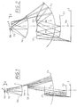
Es zeigen:
- Figur 1:
- Ein erstes erfindungsgemäßes System mit Zwischenbild und frei
zugänglicher Blende zwischen zweitem und drittem Spiegel und
numerischer
Apertur von 0,2. - Figur 2:
- Eine 6-Spiegelanordnung für Wellenlängen > 100 nm wie aus dem Stand der Technik in Form der US-A-5686728 bekannt ist.
- Figur 3:
- Eine zweite erfindungsgemäße Ausführungsform mit Blende zwischen zweitem und drittem Spiegel, die auf dem ersten Spiegel zu liegen kommt.
- Figur 4:
- Eine dritte Ausführungsform der Erfindung mit Blende auf dem zweiten Spiegel und Arbeitsabstand 59 mm.
- Figur 5:
- Eine vierte Ausführungsform der Erfindung eines Systems mit Zwischenbild, einer numerischen Apertur NA von 0,28 sowie einem bildseitigen optischen freien Arbeitsabstand, der mindestens der Summe aus einem Drittel des genutzten Durchmessers des wafernächsten Spiegels und einer Länge, die zwischen 20 und 30 mm liegt, entspricht.
- Figur 6:
- Eine fünfte Ausführungsform der Erfindung eines Systems mit Zwischenbild und einer numerischen Apertur NA von 0,30.
- Figur 7A - 7B:
- Definition des genutzten Durchmessers bei unterschiedlich ausgeleuchteten Lichtfeldern.
- Figure 1:
- A first system according to the invention with an intermediate image and a freely accessible diaphragm between the second and third mirror and a numerical aperture of 0.2.
- Figure 2:
- A 6-mirror arrangement for wavelengths> 100 nm as is known from the prior art in the form of US-A-5686728.
- Figure 3:
- A second embodiment according to the invention with an aperture between the second and third mirror, which comes to rest on the first mirror.
- Figure 4:
- A third embodiment of the invention with an aperture on the second mirror and working distance 59 mm.
- Figure 5:
- A fourth embodiment of the invention of a system with an intermediate image, a numerical aperture NA of 0.28 and an optical free working distance on the image side, which is at least the sum of one third of the diameter used of the next mirror and a length which is between 20 and 30 mm, corresponds.
- Figure 6:
- A fifth embodiment of the invention of a system with an intermediate image and a numerical aperture NA of 0.30.
- Figures 7A - 7B:
- Definition of the diameter used for differently illuminated light fields.
In den nachfolgenden Figuren 1 sowie 3 bis 4 sind Anordnungen von erfindungsgemäßen 6-Spiegel-Projektionsobjektiven gezeigt, die einen freien optischen Arbeitsabstand, der mindestens dem genutzten Durchmesser des wafernächsten Spiegels entspricht, aufweisen.In the following Figures 1 and 3 to 4 are arrangements of 6-mirror projection lenses according to the invention shown that a free optical working distance of at least the diameter used which corresponds to the next mirror.
Figur 2 zeigt demgegenüber ein System gemäß dem Stand der Technik für Wellenlängen > 100 nm, wie beispielsweise aus der US-A-5686728 bekannt.In contrast, FIG. 2 shows a system according to the prior art for Wavelengths> 100 nm, as known for example from US-A-5686728.
In sämtlichen Ausführungsformen werden nachfolgend für gleiche Bauelemente gleiche Bezugsziffern verwendet, wobei nachfolgende Nomenklatur verwendet wurde:
- erster Spiegel (S1), zweiter Spiegel (S2)
- dritter Spiegel (S3), vierter Spiegel (S4)
- fünfter Spiegel (S5), sechster Spiegel (S6).
- first mirror (S1), second mirror (S2)
- third mirror (S3), fourth mirror (S4)
- fifth mirror (S5), sixth mirror (S6).
In Figur 1 ist ein 6-Spiegel-Projektionsobjektiv gemäß der Erfindung mit Strahlengang von der Retikelebene 2 bis zur Waferebene 4 dargestellt. Die dargestellte spezielle Ausgestaltung des erfindungsgemäßen Systems kann aufgefaßt werden als Hintereinanderschaltung
- eines Feldspiegels S1, der mit Abbildungsmaßstab β > 0 ein virtuelles Bild eines Objektes erzeugt,
- eines aus S2, S3 und S4 gebildeten 3-Spiegelsystems, welches eine reelle, verkleinerte Abbildung des von S1 erzeugten virtuellen Bildes des Objektes in das System-Zwischenbild Z bewirkt und
- eines 2-Spiegelsstems S5, S6, welches das Zwischenbild Z unter
Einhaltung der Telezentrieanforderungen in
die Waferebene 4 abbildet.
- a field mirror S1, which generates a virtual image of an object with magnification β> 0,
- a 3-mirror system formed from S2, S3 and S4, which effects a real, reduced image of the virtual image of the object generated by S1 in the system intermediate image Z and
- of a 2-mirror system S5, S6, which maps the intermediate image Z into the
wafer level 4 while observing the telecentricity requirements.
Die Aberrationen der Subsysteme sind dabei so gegeneinander ausbalanciert, daß das Gesamtsystem eine für die Anwendung hinreichende Güte besitzt.The aberrations of the subsystems are balanced against each other that the overall system is of sufficient quality for the application.
Die physikalische Blende B ist zwischen zweitem Spiegel S2 und drittem Spiegel S3 angeordnet. Wie deutlich aus Figur 1 hervorgeht, liegt die Blende zugänglich im Strahlengang zwischen zweitem Spiegel S2 und drittem Spiegel S3.The physical aperture B is between the second mirror S2 and the third Mirror S3 arranged. As is clear from Figure 1, the aperture is accessible in the beam path between the second mirror S2 and the third Mirror S3.
Beim System gemäß Figur 1 ist der optische Arbeitsabstand zwischen dem
wafernächsten Spiegel, das ist in vorliegendem Ausführungsbeispiel der fünfte
Spiegel S5, und der Waferebene 4 größer als der genutzte Durchmesser des
Spiegels S5, d.h. es ist nachfolgende Bedingung erfüllt:
optischer Abstand S5 zur Waferebene 4 > genutzter Durchmesser S5.In the system according to FIG. 1, the optical working distance between the next mirror next to the wafer, that is the fifth mirror S5 in the present exemplary embodiment, and the
optical distance S5 to
Auch andere Abstandsbedinungen sind alternativ möglich, beispielsweise daß der optische Arbeitsabstand größer als die Summe aus ein Drittel des genutzten Durchmessers des wafernächsten Spiegels S5 plus 20 mm oder mehr als 50 mm ist.Other distance conditions are alternatively possible, for example that the optical working distance is greater than the sum of one third of the used diameter of the next mirror S5 plus 20 mm or is more than 50 mm.
Im vorliegenden Ausführungsbeispiel beträgt der freie optische Arbeitsabstand 60 mm, ohne hierauf beschränkt zu sein. In the present exemplary embodiment, the free optical working distance is 60 mm without being limited to this.
Ein derartiger optischer Arbeitsabstand garantiert einen ausreichend freien mechanischen Arbeitsabstand, der größer als 0 ist sowie die Verwendung von optischen Komponenten mit ausreichenden Festigkeitseigenschaften für Wellenlängen < 100 nm, vorzugsweise von 11 bzw. 13 nm.Such an optical working distance guarantees a sufficiently free one mechanical working distance that is greater than 0 and the use of optical components with sufficient strength properties for Wavelengths <100 nm, preferably 11 or 13 nm.
Die optischen Komponenten umfassen für eine Wellenlänge λ = 13 nm und λ = 11 nm beispielsweise Mo/Si- bzw. Mo/Be-Multilayer-Schichtsysteme, wobei typische Multilayer-Schichtsysteme für λ = 13 nm 40 Mo/Si-Schichtpaare und für λ = 11 nm taugliche Mo/Be-Systeme ungefähr 70 Schichtpaare aufweisen. Die erreichbaren Reflektivitäten der Systeme liegen im Bereich von ungefähr 70 %. In den Multilayer-Schichtsystemen können Schichtspannungen von 350 MPa und mehr auftreten, die Oberflächendeformation, insbesondere in den Randbereichen der Spiegel induzieren.For a wavelength, the optical components include λ = 13 nm and λ = 11 nm, for example Mo / Si or Mo / Be multilayer coating systems, where typical multilayer layer systems for λ = 13 nm 40 Mo / Si layer pairs and for λ = 11 nm suitable Mo / Be systems about 70 Have layer pairs. The reflectivities of the systems are achievable in the range of approximately 70%. In the multilayer coating systems can Layer stresses of 350 MPa and more occur that Surface deformation, especially in the edge areas of the mirrors induce.
Die erfindungsgemäßen Systeme, wie beispielsweise in Figur 1 dargestellt,
besitzen gemäß
Des weiteren ist der Strahlengang des in Fig. 1 dargestellten Objektives obskurationsfrei. Um beispielsweise Bildformate von 26 x 34 mm2 bzw. 26 x 52 mm2 bereitzustellen, werden die erfindungsgemäßen Projektionsobjektive vorzugsweise in Ringfeld-Scan-Projektionsbelichtungsanlagen verwendet, wobei die Sekantenlänge des Scan-Schlitzes mindestens 26 mm beträgt. Furthermore, the beam path of the objective shown in FIG. 1 is free of obscuration. In order to provide, for example, image formats of 26 x 34 mm 2 or 26 x 52 mm 2 , the projection objectives according to the invention are preferably used in ring field scan projection exposure systems, the secant length of the scan slot being at least 26 mm.
Je nach verwandter Maske in der Projektionsbelichtungsanlage, hier sind Transmissionsmasken z.B. Stencilmasken oder auch Reflektionsmasken denkbar, kann das bildseitig telezentrische System objektseitig telezentrisch oder nicht telezentrisch ausgebildet werden, wobei ein telezentrischer Strahlengang objektseitig bei Verwendung einer Reflektionsmakse nur unter Verwendung eines transmissionsmindernden Strahlenteilers möglich ist. Unebenheiten der Maske führen bei nicht telezentrischem Strahlengang im Objektraum zu Maßstabsfehlern in der Abbildung. Die Hauptstrahlwinkel am Retikel liegen daher vorzugsweise unter 10°, damit die Anforderungen an die Retikelebenheit im Bereich des technologisch realisierbaren liegen.Depending on the mask used in the projection exposure system, here are Transmission masks e.g. Stencil masks or reflection masks conceivable, the telecentric system on the image side can be telecentric on the object side or not be telecentric, being a telecentric Beam path on the object side only when using a reflection lens Use of a transmission-reducing beam splitter is possible. Unevenness of the mask result in a non-telecentric beam path in the Object space for scale errors in the figure. The main beam angles on Reticles are therefore preferably below 10 °, so that the requirements for Flatness of the reticle lies in the range of technologically feasible.
Das erfindungsgemäße System gemäß Figur 1 weist einen bildseitigen Telezentriefehler am Wafer von 1 mrad bei einer numerischen Apertur von 0,2 auf.The system according to the invention according to FIG. 1 has an image side Telecentricity error on the wafer of 1 mrad with a numerical aperture of 0.2 on.
Aufgrund der hohen bildseitigen Telezentrie liegt die Eintrittspupille des letzten Spiegel S6 in oder nahe seines Brennpunktes. Bei den erfindungsgemäßen Systemen mit Zwischenbild kommt die Blende dann im vorderen, niederaperturigen Objektivteil vorwiegend zwischen dem ersten und dritten Spiegel S1, S3 zum Liegen und die dazu konjugierte Pupillenebene wird in den Fokus des letzten Spiegels abgebildet.Due to the high image-side telecentricity, the entrance pupil of the last one is located Mirror S6 at or near its focal point. In the invention In systems with an intermediate image, the aperture comes in the front, low-aperture lens part mainly between the first and third Mirrors S1, S3 for lying and the pupil plane conjugated to it is shown in the focus of the last mirror.
In der dargestellten Ausführungsform sind sämtliche Spiegel S1 - S6 asphärisch ausgeführt, wobei die maximale Asphärizität im Nutzbereich bei 7,3 µm liegt. Die niedrige Asphärizität der erfindungsgemäßen Anordnung ist insbesondere aus fertigungstechnischer Sicht vorteilhaft, da die technologischen Schwierigkeiten bei der Bearbeitung der Oberflächen der Multilayer-Spiegel mit der asphärischen Abweichung und wachsendem Gradienten der Asphäre überproportional stark ansteigen. In the illustrated embodiment, all mirrors are S1-S6 made aspherical, the maximum asphericity in the useful area at 7.3 µm. The low asphericity of the arrangement according to the invention is Particularly advantageous from a manufacturing point of view, since the technological difficulties in machining the surfaces of the Multilayer mirror with the aspherical deviation and growing Gradients of the asphere increase disproportionately.
Der größe Einfallswinkel in der Anordnung gemäß Figur 1 tritt an S5 auf und beträgt 18,4°. An Spiegel S5 tritt auch die maximale Einfallswinkelvariation von ca. 14,7° über den Spiegel hinweg auf. Der Wellenfrontfehler der Anordnung gemäß Figur 1 bei λ = 13 nm ist besser als 0,032 λ, die Schwerpunktverschiebung der Punktbilder ist < 3 nm, die statische, maßstabskorrigierte Verzeichnung liegt bei 4 nm.The large angle of incidence in the arrangement according to FIG. 1 occurs at S5 and is 18.4 °. The maximum angle of incidence of mirror occurs at mirror S5 about 14.7 ° above the mirror. The wavefront error of the arrangement according to Figure 1 at λ = 13 nm is better than 0.032 λ that Center of gravity shift of the point images is <3 nm, the static, scale-corrected distortion is 4 nm.
Die in der Ausführungsform gemäß Figur 1 zwischen zweitem und dritten
Spiegel angeordnete Blende ist frei zugänglich. Eine freie Zugängigkeit der
Blende und eine Abschattung des von S3 nach S4 laufenden Bündels durch
die Blende wird bei gleichzeitig akzeptablen Einfallswinkeln auf den Spiegeln
verhindert, wenn in den dargestellten Anordnungen, nachfolgende
Bedingung
Hierbei bezeichnet die Kurzschreibweise S1S3 den mechanischen Abstand zwischen den einzelnen Komponenten, hier den Spiegeln S1 und S3.The short form S1S3 denotes the mechanical distance between the individual components, here mirrors S1 and S3.
Um die Einfallswinkel auf den Spiegeln zu vermindern ist in einer besonders
bevorzugten Ausführungsform der Erfindung gemäß Fig. 1 und Fig. 3-4 der
Abstand vom Retikel zu S1 kleiner als der Abstand von S2 zu S3, d.h. es gilt:
Für die mechanische Realisierung ist es besonders vorteilhaft, wenn das Retikel physikalisch hinreichend weit vor dem in Lichtrichtung ersten Spiegel - hier S2 - zu liegen kommt.For the mechanical implementation, it is particularly advantageous if that Reticle physically sufficiently far in front of the first mirror in the direction of light - here S2 - comes to rest.
Vorliegend beträgt der Abstand Retikel S2 80 mm, ohne hierauf beschränkt zu sein.In the present case, the distance between reticle S2 is 80 mm, without being restricted to this his.
Des weiteren ist bei der Ausführungsform der Erfindung gemäß den Figuren 1 sowie 3 bis 5 der Abstand zwischen den Spiegeln S3 und S6 so groß gewählt, daß die Spiegel hinreichend dick ausgebildet werden können, um bei den auftretenden hohen Schichtspannungen über die geforderten Festigkeitseigenschaften zu verfügen.Furthermore, in the embodiment of the invention according to FIGS and 3 to 5 the distance between the mirrors S3 and S6 so large chosen that the mirror can be made sufficiently thick to in the case of the high layer tensions that occur above the required To have strength properties.
Besonders bevorzugt ist es, wenn nachfolgende Beziehung vorliegt:It is particularly preferred if the following relationship exists:
0,3 (genutzter Durchmesser S3 + genutzter Durchmesser S6) < S3S6.0.3 (used diameter S3 + used diameter S6) <S3S6.
Aus der nachfolgenden Tabelle gehen in Code V-Nomenklatur die Parameter
der beispielhaft in Figur 1 dargestellten Systeme hervor. Bei dem Objektiv
handelt es sich um 5x-System mit einem 26 x 2 mm2 Ringfeld und einer
numerischen Apertur von 0,2. Der mittlere bildseitige Radius des Systems
beträgt dabei ungefähr 26 mm.

In Figur 2 ist eine Anordnung eines Projektionsobjektives für die Mikrolithographie mit Wellenlänge λ < 100 nm gemäß der US-A-5686728 gezeigt. Gleiche Bauteile wie in Figur 1 sind mit denselben Bezugsziffern belegt.FIG. 2 shows an arrangement of a projection lens for the Microlithography with wavelength λ <100 nm according to US-A-5686728 shown. The same components as in Figure 1 are given the same reference numerals busy.
Wie deutlich zu erkennen, ist der Abstand zwischen dem wafernächsten Spiegel S5 und dem Wafer wesentlich geringer als der Durchmesser des Spiegels und liegt vorliegend im Bereich von ungefähr 20 mm, was im EUV-Bereich aufgrund der extremen Schichtspannungen zu Festigkeitsproblemen führt.As can be clearly seen, the distance between the next wafer Mirror S5 and the wafer much smaller than the diameter of the Mirror and in the present case is in the range of approximately 20 mm, which is in the EUV range due to the extreme layer stresses to strength problems leads.
Des weiteren weist das System gemäß dem Stand der Technik sehr hohe Asphärizitäten von +/- 50 µm und Einfallswinkel von 38° auf. Derartige Asphärizitäten und Einfallswinkel sind im EUV-Bereich unter dem Blickwinkel der Fertigungs- und Beschichtungstechnologie nicht realisierbar.Furthermore, the system according to the prior art has very high Asphericities of +/- 50 µm and angle of incidence of 38 °. Such Asphericities and angles of incidence are in the EUV range from the perspective manufacturing and coating technology not feasible.
In Figur 3 ist eine alternative Ausführungsform eines erfindungsgemäßen 6-Spiegelsystems dargestellt, bei dem die Blende auf dem ersten Spiegel liegt. Gleiche Bauteile wie in Figur 1 werden wiederum mit denselben Bezugsziffern belegt. In Figure 3 is an alternative embodiment of an inventive 6-mirror system shown, in which the aperture on the first mirror lies. The same components as in Figure 1 are again the same Reference numbers occupied.
Der optische freie Arbeitsabstand am Wafer beträgt auch bei dieser Ausführungsform wie schon bei der Ausführungsform gemäß Figur 1 60 mm und ist somit größer als der Durchmesser des wafernächsten Spiegels S5. Wie bei der Ausführungsform gemäß Figur 1 ist auch bei dem Design gemäß Figur 3 der Abstand zwischen S2 und S3 gegenüber dem Stand der Technik in Form der US-A-5686728 wesentlich erhöht worden, so daß große Inzidenzwinkel im System vermindert werden.The optical free working distance on the wafer is also this Embodiment as in the embodiment according to FIG. 1 60 mm and is therefore larger than the diameter of the mirror S5 next to the wafer. As with the embodiment according to FIG. 1, the design according to FIG Figure 3 shows the distance between S2 and S3 compared to the prior art in the form of US-A-5686728 has been increased significantly so that large Incidence angles in the system can be reduced.
Im Unterschied zu der Ausgestaltung gemäß Figur 1 ist in Figur 3 die Blende B physikalisch auf den Primärspiegel gelegt. Durch diese Position wird eine sehr effiziente Abschaltung von an S2 reflektiertem Licht möglich, das bei einer physikalischen Blendenposition zwischen S1 und S2 leicht oberhalb der als schmalen Ring auszubildenden Blende passieren könnte. Bei dem in Figur 3 dargestellten Ausführungsbeispiel kann die Blende entweder als Öffnung im S1-Mutterspiegel oder hinter S1 liegend realisiert werden.In contrast to the configuration according to FIG. 1, the diaphragm is in FIG. 3 B physically placed on the primary mirror. Through this position a very efficient switching off of light reflected at S2 possible, which at a physical aperture position between S1 and S2 slightly above the could pass as a narrow ring to be trained. In the figure The embodiment shown in FIG. 3 can either be an opening in the S1 mother mirror or behind S1.
Ein weiterer Vorteil der Lösung gemäß Figur 3 ist die sphärische Ausbildung
des Spiegels S4, die insbesondere unter Fertigungsaspekten einen
besonderen Vorteil darstellt, da der Spiegel S4 der größte Spiegel des
Systems ist. Gegenüber der Ausführungsform gemäß Figur 1 ist bei der
Ausgestaltung gemäß Figur 3 die Asphärizität im Nutzbereich leicht erhöht
und liegt bei 10,5 µm. Der größte Einfallswinkel tritt wie bei der
Ausführungsform gemäß Figur 1 an Spiegel S5 auf und beträgt ca. 18,6°. Der
Wellenfrontfehler der Anordnung gemäß Figur 3 beträgt 0,032 λ, innerhalb
des 1,7 mm breiten Ringfeldes bei λ = 13 nm. Bildet man den Spiegel S4 bei
der Ausgestaltung gemäß Figur 3 leicht asphärisch aus mit 0,4 µm, so kann
der Wellenfrontfehler auf 0,031 λ innerhalb eines 1,8 mm breiten Ringfeldes
bei λ = 13 nm gehalten werden. Eine effiziente Ausblendung unerwünschten
Lichtes erhält man nicht nur, wenn man die Blende direkt auf dem Spiegel S1
ausbildet, sondern auch dann, wenn man sie dem Spiegel S1 nachordnet.
Eine besonders bevorzugte Baubedingung für eine derartige Blende ist:
In Tabelle 2 sind die Konstruktionsdaten des 5x Objektives gemäß Figur 3 in
Code V-Nomenklatur dargestellt, wobei der vierte Spiegel S4 sphärisch
ausgebildet ist. Der mittlere Radius des 26 x 1,7 mm2 - Bildfeldes beträgt
wiederum 26 mm.


In Figur 4 ist eine weitere Ausführungsform der Erfindung gezeigt, wobei wiederum für gleiche Bauteile dieselben Bezugsziffern wie in den vorausgegangenen Figuren verwendet wurden.A further embodiment of the invention is shown in FIG again for the same components the same reference numerals as in the previous figures were used.
Bei der Ausführungsform gemäß Figur 4 wurde die Blende B optisch und physikalisch auf den Sekundärspiegel bzw. zweiten Spiegel S2 gelegt.In the embodiment according to FIG. 4, the aperture B was optically and physically placed on the secondary mirror or second mirror S2.
Die Anordnung der Blende direkt auf dem Spiegel hat den Vorteil, daß diese Blende auf einem Spiegel sich mechanisch einfacher realisieren läßt.The arrangement of the diaphragm directly on the mirror has the advantage that this Aperture on a mirror is easier to implement mechanically.
Mit dem in Figur 4 dargestellten 4x Aufbau läßt sich innerhalb eines 2 mm breiten Ringfeldes ein Wellenfrontfehler bei λ = 13 nm von 0,021 λ realisieren. Die maximale Asphärizität im Nutzbereich liegt bei 11,2 µm, der größte an S5 auftretende Einfallswinkel beträgt 18,3°. Der mittlere Bildfeldradius beträgt wiederum 26 mm.With the 4x structure shown in Figure 4 can be within a 2 mm wide wavefront realize a wavefront error at λ = 13 nm of 0.021 λ. The maximum asphericity in the useful area is 11.2 µm, the largest at S5 angle of incidence is 18.3 °. The average field radius is again 26 mm.
Erfindungsgemäß ist der optische freie Arbeitsabstand zwischen Wafer und wafernächstem Spiegel S5 erfindungsgemäß größer als der Durchmesser des wafernächsten Spiegels S5 und liegt in vorliegender Ausführungsform bei ca. 59 mm. According to the invention, the optical free working distance between the wafer and wafer next mirror S5 larger than the diameter of the invention next to the mirror S5 and in the present embodiment is approx. 59 mm.
In Tabelle 3 sind die optischen Parameter in Code V-Nomenklatur der in Figur
4 dargestellten Ausführungsform der Erfindung aufgeführt.


Figur 5 zeigt eine Ausführungsform der Erfindung, die einen Feldspiegel S1,
ein erstes Subsystem mit zweitem bis viertem Spiegel S2 - S4 und ein zweites
Subsystem mit fünftem und sechstem Spiegel S5, S6 umfaßt. Der Feldspiegel
S1 mit β > 0 erzeugt ein virtuelles Bild des Objektes 2, welches durch das
aus zweitem, drittem und viertem Spiegel S2, S3, S4 gebildeten erste
Subsystem mit β < 0 reell in das Zwischenbild Z abgebildet wird, wobei das
aus fünftem und sechstem Spiegel S5, S6 gebildete zweite Subsystem das
Zwischenbild Z in das reelle Systembild der Waferebene 4 abbildet. Die
numerische Apertur des Systems beträgt NA = 0,28. Der Arbeitsabstand
zwischen letztem Spiegel S5 und der Waferebene entspricht mindestens der
Summe aus einem Drittel des genutzten Durchmessers des wafernächsten
Spiegels und einer Länge, die zwischen 20 und 30 mm liegt. Die Blende B
kommt auf dem zweiten Spiegel S2 zum Liegen.FIG. 5 shows an embodiment of the invention, which has a field mirror S1,
a first subsystem with second to fourth mirrors S2 - S4 and a second
Subsystem with fifth and sixth mirrors S5, S6 comprises. The field mirror
S1 with β> 0 generates a virtual image of the
In Tabelle 4 sind die optischen Parameter der Ausführungsform gemäß Figur
5 in Code V-Nomenklatur aufgeführt.

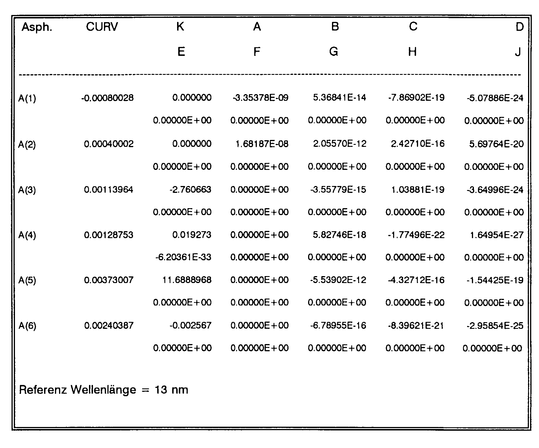
In Figur 6 ist eine zweite Ausführungsform eines 6-Spiegel-Objektives mit Feldspiegel S1, erstem und zweitem Subsystem sowie Zwischenbild Z gezeigt. Die numerische Apertur NA dieses Systems liegt bei NA = 0,30; die Blende B wird wie bei der Ausführungsform gemäß Figur 5 auf dem zweiten Spiegel S2 ausgebildet.FIG. 6 shows a second embodiment of a 6-mirror lens Field mirror S1, first and second subsystem and intermediate image Z shown. The numerical aperture NA of this system is NA = 0.30; the As in the embodiment according to FIG. 5, aperture B becomes second Mirror S2 formed.
Die optischen Parameter der Ausführungsform gemäß Figur 6 sind in Tabelle
5 in Code V-Nomenklatur aufgeführt.

Die Figuren 7A und 7B verdeutlichen nochmals was in der vorliegenden Anmeldung unter dem genutzten Durchmesser D zu verstehen ist.FIGS. 7A and 7B again illustrate what is in the present Registration is to be understood under the diameter D used.
Beispielhaft sei das ausgeleuchtete Feld 100 auf einem Spiegel in Figur 7A
ein Rechteckfeld. Der genutzte Durchmesser D ist dann der Durchmesser
des Hüllkreises 102, der das Rechteck 100 umschließt, wobei die Ecken 104
des Rechteckes 100 auf den Hüllkreis 102 zu liegen kommen.The
In Figur 7B ist ein zweites Beispiel dargestellt. Das ausgeleuchtete Feld 100
weist eine Nierenform auf, wie für den Nutzbereich bei Verwendung der
erfindungsgemäßen Objektive in einer Mikrolithographie-Projektionsbelichtungsanlage
erwartet. Der Hüllkreis 102 umschließt die
Nierenform völlig und fällt an zwei Punkten 106, 108 mit dem Rand 110 der
Nierenform zusammen. Der genutzte Durchmesser D ergibt sich dann aus
dem Durchmesser des Hüllkreises 102.A second example is shown in FIG. 7B. The
Mit der Erfindung wird somit erstmals ein 6-Spiegel-Projektionsobjektiv mit einem Abbildungsmaßstab von vorzugsweise 4x, 5x sowie 6x für den bevorzugten Einsatz in einem EUV-Ringfeldprojektionssystem angegeben, das sowohl die notwendige Auflösung bei gefordertem Bildfeld wie auch Konstruktionsbedingungen aufweist, welche eine funktionsgerechte Bauausführung ermöglichen, da die Asphären hinreichend mild, die Winkel hinreichend klein für die Schichten und die Bauräume für die Spiegelträger hinreichend groß sind.With the invention, a 6-mirror projection lens is thus used for the first time a magnification of preferably 4x, 5x and 6x for the preferred use in an EUV ring field projection system specified that both the necessary resolution for the required image field as well Design conditions, which has a functional Construction allows the angles because the aspheres are sufficiently mild sufficiently small for the layers and the installation space for the mirror supports are sufficiently large.
Claims (32)
dadurch gekennzeichnet, daß
die bildseitige numerische Apertur NA ≥ 0,15 ist und der dem zu belichtenden Objekt vorzugsweise dem Wafer am nächsten kommende Spiegel derart angeordnet ist, daß
characterized in that
the numerical aperture on the image side is NA 0,1 0.15 and the mirror closest to the object to be exposed is preferably arranged in such a way that
dadurch gekennzeichnet, daß
die bildseitige numerische Apertur (NA) im Bereich
und daß die Spitze-Spitze-Abweichung (A) der Asphären gegenüber der im Nutzbereich bestpassenden Sphäre auf allen Spiegeln durch
characterized in that
the numerical aperture (NA) in the area
and that the tip-to-tip deviation (A) of the aspheres compared to the best-fitting sphere in the usable area occurs on all mirrors
dadurch gekennzeichnet, daß
die bildseitige numerische Apertur (NA) ≥ 0,15 ist,
die bildseitige Breite des Ringfeldes W ≥ 1,0 mm ist und
daß die Einfallswinkel (AOI) relativ zur Flächennormalen aller Strahlen auf allen Spiegeln durch
characterized in that
the image-side numerical aperture (NA) is ≥ 0.15,
the image-side width of the ring field W ≥ 1.0 mm and
that the angle of incidence (AOI) is relative to the surface normal of all rays on all mirrors
einem Feldspiegel S1, einem ersten Subsystem mit zweitem bis viertem Spiegel (S2 - S4) und einem zweiten Subsystem mit fünftem und sechstem Spiegel (S5, S6),
dadurch gekennzeichnet, daß
der Feldspiegel mit β > 0 ein virtuelles Bild des Objektes (2) erzeugt, welches durch das aus zweitem, drittem und viertem Spiegel (S2, S3, S4) gebildete erste Subsystem mit β < 0 reell in das Zwischenbild (Z) abgebildet wird, wobei das aus fünftem und sechstem Spiegel (S5, S6) gebildete zweite Subsystem das Zwischenbild in das reelle Systembild in der Waferebene (4) abbildet.Microlithography projection lens device with
a field mirror S1, a first subsystem with second to fourth mirrors (S2 - S4) and a second subsystem with fifth and sixth mirrors (S5, S6),
characterized in that
the field mirror with β> 0 generates a virtual image of the object (2), which is mapped into the intermediate image (Z) by the first subsystem with β <0, formed from the second, third and fourth mirror (S2, S3, S4), wherein the second subsystem formed from the fifth and sixth mirrors (S5, S6) maps the intermediate image into the real system image in the wafer plane (4).
dadurch gekennzeichnet, daß
der dem zu belichtenden Objekt vorzugsweise dem Wafer am nächsten kommenden Spiegel derart angeordnet ist, daß
characterized in that
the mirror closest to the object to be exposed is preferably arranged in such a way that
die bildseitige numerische Apertur NA im Bereich
the numerical aperture NA in the area
dadurch gekennzeichnet, daß
die Spiegel derart angeordnet sind, daß die Lichtführung obskurationsfrei ist.Microlithography projection lens device according to one of claims 1 to 6,
characterized in that
the mirrors are arranged in such a way that the light is free from obscuration.
dadurch gekennzeichnet, daß
die Spiegelflächen auf zu einer Hauptachse (HA) rotationssymmetrischen Flächen angeordnet sind.Microlithography projection lens device according to one of claims 1 to 7,
characterized in that
the mirror surfaces are arranged on surfaces that are rotationally symmetrical to a main axis (HA).
dadurch gekennzeichnet, daß
im Projektionsobjektiv nach dem vierten Spiegel (S4) ein Zwischenbild ausgebildet wird.Microlithography projection lens device according to one of claims 1 to 8,
characterized in that
an intermediate image is formed in the projection lens after the fourth mirror (S4).
dadurch gekennzeichnet, daß
eine Blende (B) im Lichtweg bzw. Strahlengang zwischen zweitem (S2) und drittem Spiegel (S3) angeordnet ist.Microlithography projection lens device according to claim 9,
characterized in that
an aperture (B) is arranged in the light path or beam path between the second (S2) and third mirror (S3).
dadurch gekennzeichnet, daß
die Abstände zwischen erstem, zweitem und drittem Spiegel derart gewählt werden, daß die Blende frei zugänglich ist. Microlithography projection lens device according to claim 10,
characterized in that
the distances between the first, second and third mirror are chosen such that the diaphragm is freely accessible.
dadurch gekennzeichnet, daß
der Abstand von erstem und drittem Spiegel (S1S3) zum Abstand von erstem und zweitem Spiegel (S1S2) im Bereich
characterized in that
the distance from the first and third mirror (S1S3) to the distance from the first and second mirror (S1S2) in the area
dadurch gekennzeichnet, daß
die Blende (B) im Strahlengang zwischen zweitem (S2) und drittem Spiegel (S3) am Körper des ersten Spiegels (S1) angeordnet ist.Microlithography projection lens device according to one of claims 1 to 12,
characterized in that
the diaphragm (B) is arranged in the beam path between the second (S2) and third mirror (S3) on the body of the first mirror (S1).
dadurch gekennzeichnet, daß
die bildseitige numerische Apertur NA ≥ 0,15 und die Ringfeldbreite am Wafer W ≥ 1 mm ist und
daß die Spitze-Spitze-Abweichung (A) der Asphären gegenüber der im Nutzbereich bestpassenden Sphären auf allen Spiegeln durch
characterized in that
the image-side numerical aperture NA ≥ 0.15 and the ring field width on the wafer W ≥ 1 mm and
that the tip-to-tip deviation (A) of the aspheres compared to the spheres best fitting in the useful area on all mirrors
dadurch gekennzeichnet, daß
die Blende (B) auf oder nahe beim zweiten Spiegel (S2) angeordnet ist. Microlithography projection lens device according to one of claims 1 to 8,
characterized in that
the diaphragm (B) is arranged on or near the second mirror (S2).
dadurch gekennzeichnet, daß
der Abstand vom ersten und dritten Spiegel (S1S3) zum Abstand von erstem und zweitem Spiegel (S1S2) im Bereich
characterized in that
the distance from the first and third mirror (S1S3) to the distance from the first and second mirror (S1S2) in the area
dadurch gekennzeichnet, daß
sämtliche Spiegel asphärisch ausgebildet sind.Microlithography projection lens device according to one of Claims 1 to 16,
characterized in that
all mirrors are aspherical.
dadurch gekennzeichnet, daß
höchstens fünf Spiegel asphärisch sind.Microlithography projection lens device according to one of Claims 1 to 16,
characterized in that
a maximum of five mirrors are aspherical.
dadurch gekennzeichnet, daß
der zweite bis sechste Spiegel (S2 - S6) in der Reihenfolge konkavkonvex-konkav-konvex-konkav ausgebildet ist.Microlithography projection objective device according to one of Claims 1 to 18,
characterized in that
the second to sixth mirrors (S2 - S6) are designed in the order concave-convex-concave-convex-concave.
dadurch gekennzeichnet, daß
der Abbildungsmaßstab des ersten Spiegels (S1) positiv ist, vorzugsweise 0,5 < β < 1,5.Microlithography projection lens device according to one of claims 1 to 19,
characterized in that
the imaging scale of the first mirror (S1) is positive, preferably 0.5 <β <1.5.
dadurch gekennzeichnet, daß
der Abbildungsmaßstab des aus zweitem (S2), drittem (S3) und viertem Spiegel (S4) gebildeten Subsystems negativ und verkleinernd ist, vorzugsweise - 0,5 > β > - 1,0.Microlithography projection lens device according to one of claims 1 to 19,
characterized in that
the imaging scale of the subsystem formed from the second (S2), third (S3) and fourth mirror (S4) is negative and reducing, preferably - 0.5>β> - 1.0.
dadurch gekennzeichnet, daß
der rms-Wellenfrontfehler des Systems höchstens 0,07 λ, bevorzugt 0,03 λ, über das gesamte Bildfeld beträgt.Microlithography projection lens device according to one of claims 1 to 21,
characterized in that
the system's rms wavefront error is at most 0.07 λ, preferably 0.03 λ, over the entire image field.
dadurch gekennzeichnet, daß
das Bildfeld mindestens 1,0 mm breit ist.Microlithography projection device according to claim 22,
characterized in that
the image field is at least 1.0 mm wide.
dadurch gekennzeichnet, daß
sie bildseitig telezentrisch ist.Microlithography projection lens device according to one of claims 1 to 23,
characterized in that
it is telecentric on the image side.
dadurch gekennzeichnet, daß
sie objektseitig telezentrisch ist.Microlithography projection lens device according to claim 24,
characterized in that
it is telecentric on the object side.
dadurch gekennzeichnet, daß
der Hauptstrahl am Objekt zur optischen Achse hinläuft.Microlithography projection objective device according to one of Claims 1 to 24,
characterized in that
the main beam on the object runs towards the optical axis.
dadurch gekennzeichnet, daß
der Spiegel mit der betragsmäßig kleinsten Brennweite nach dem Zwischenbild liegt.Microlithography projection objective device according to one of Claims 9 to 26,
characterized in that
the mirror with the smallest focal length is located according to the intermediate image.
dadurch gekennzeichnet, daß
der Abstand von drittem und sechstem Spiegel (S3S6) nachfolgender Beziehung genügt:
characterized in that
the distance between the third and sixth mirror (S3S6) of the following relationship is sufficient:
dadurch gekennzeichnet, daß
eine Reflektionsmaske vorgesehen ist.Projection exposure system with a microlithography projection objective device according to one of Claims 1 to 28,
characterized in that
a reflection mask is provided.
dadurch gekennzeichnet, daß
eine Transmissionsmaske vorgesehen ist.Projection exposure system with a microlithography projection objective device according to one of Claims 1 to 28,
characterized in that
a transmission mask is provided.
dadurch gekennzeichnet, daß
die Projektionsbelichtungsanlage eine Beleuchtungseinrichtung zur Beleuchtung eines Ringfeldes umfaßt. Projection exposure system according to one of claims 29 to 30,
characterized in that
the projection exposure system comprises an illumination device for illuminating a ring field.
Priority Applications (1)
| Application Number | Priority Date | Filing Date | Title |
|---|---|---|---|
| EP06025651A EP1772775B1 (en) | 1999-02-15 | 1999-12-23 | Microlithographic reduction lens and projection illumination system |
Applications Claiming Priority (4)
| Application Number | Priority Date | Filing Date | Title |
|---|---|---|---|
| DE19906001 | 1999-02-15 | ||
| DE19906001 | 1999-02-15 | ||
| DE19948240 | 1999-10-07 | ||
| DE19948240A DE19948240A1 (en) | 1999-02-15 | 1999-10-07 | Microlithography reduction objective lens with projection illumination installation, including its use in chip manufacture |
Related Child Applications (1)
| Application Number | Title | Priority Date | Filing Date |
|---|---|---|---|
| EP06025651A Division EP1772775B1 (en) | 1999-02-15 | 1999-12-23 | Microlithographic reduction lens and projection illumination system |
Publications (3)
| Publication Number | Publication Date |
|---|---|
| EP1035445A2 true EP1035445A2 (en) | 2000-09-13 |
| EP1035445A3 EP1035445A3 (en) | 2003-04-23 |
| EP1035445B1 EP1035445B1 (en) | 2007-01-31 |
Family
ID=26051832
Family Applications (2)
| Application Number | Title | Priority Date | Filing Date |
|---|---|---|---|
| EP06025651A Expired - Lifetime EP1772775B1 (en) | 1999-02-15 | 1999-12-23 | Microlithographic reduction lens and projection illumination system |
| EP99125783A Expired - Lifetime EP1035445B1 (en) | 1999-02-15 | 1999-12-23 | Microlithographic reduction objective and projection exposure apparatus |
Family Applications Before (1)
| Application Number | Title | Priority Date | Filing Date |
|---|---|---|---|
| EP06025651A Expired - Lifetime EP1772775B1 (en) | 1999-02-15 | 1999-12-23 | Microlithographic reduction lens and projection illumination system |
Country Status (5)
| Country | Link |
|---|---|
| US (1) | US6353470B1 (en) |
| EP (2) | EP1772775B1 (en) |
| JP (1) | JP2000235144A (en) |
| DE (1) | DE59914179D1 (en) |
| TW (1) | TW464768B (en) |
Cited By (4)
| Publication number | Priority date | Publication date | Assignee | Title |
|---|---|---|---|---|
| EP1178356A2 (en) * | 2000-08-01 | 2002-02-06 | Carl Zeiss | 6 mirror microlithography projection system |
| US6867913B2 (en) | 2000-02-14 | 2005-03-15 | Carl Zeiss Smt Ag | 6-mirror microlithography projection objective |
| US6927403B2 (en) | 2001-08-10 | 2005-08-09 | Carl Zeiss Smt Ag | Illumination system that suppresses debris from a light source |
| US7030965B2 (en) | 2000-10-23 | 2006-04-18 | Nikon Corporation | Catadioptric system and exposure device having this system |
Families Citing this family (70)
| Publication number | Priority date | Publication date | Assignee | Title |
|---|---|---|---|---|
| DE10053587A1 (en) * | 2000-10-27 | 2002-05-02 | Zeiss Carl | Lighting system with variable adjustment of the illumination |
| US7329886B2 (en) * | 1998-05-05 | 2008-02-12 | Carl Zeiss Smt Ag | EUV illumination system having a plurality of light sources for illuminating an optical element |
| US6577443B2 (en) * | 1998-05-30 | 2003-06-10 | Carl-Zeiss Stiftung | Reduction objective for extreme ultraviolet lithography |
| EP1093021A3 (en) * | 1999-10-15 | 2004-06-30 | Nikon Corporation | Projection optical system as well as equipment and methods making use of said system |
| TW538256B (en) * | 2000-01-14 | 2003-06-21 | Zeiss Stiftung | Microlithographic reduction projection catadioptric objective |
| JP2004512552A (en) * | 2000-10-20 | 2004-04-22 | カール ツァイス シュティフトゥング トレイディング アズ カール ツァイス | 8 Reflection mirror type projection optical system for microlithography |
| DE10052289A1 (en) * | 2000-10-20 | 2002-04-25 | Zeiss Carl | 8 mirror microlithography projection lens |
| TW573234B (en) * | 2000-11-07 | 2004-01-21 | Asml Netherlands Bv | Lithographic projection apparatus and integrated circuit device manufacturing method |
| KR100831706B1 (en) * | 2001-01-09 | 2008-05-22 | 칼 짜이스 에스엠티 에이지 | Projection system for euv lithography |
| JP2002329655A (en) * | 2001-05-01 | 2002-11-15 | Canon Inc | Reflection type contraction projection optical system, aligner and device manufacturing method |
| JP2003015040A (en) * | 2001-07-04 | 2003-01-15 | Nikon Corp | Projection optical system and exposure device equipped therewith |
| EP1282011B1 (en) | 2001-08-01 | 2006-11-22 | Carl Zeiss SMT AG | Reflective projection lens for EUV photolithography |
| DE10139177A1 (en) * | 2001-08-16 | 2003-02-27 | Zeiss Carl | Objective with pupil obscuration |
| JP2003233001A (en) * | 2002-02-07 | 2003-08-22 | Canon Inc | Reflection type projection optical system, exposure device, and method for manufacturing device |
| US7428037B2 (en) * | 2002-07-24 | 2008-09-23 | Carl Zeiss Smt Ag | Optical component that includes a material having a thermal longitudinal expansion with a zero crossing |
| JP2005536900A (en) * | 2002-08-26 | 2005-12-02 | カール・ツァイス・エスエムティー・アーゲー | A grating-based spectral filter that removes a band of radiation within an extreme ultraviolet lithography system |
| JP2006501660A (en) * | 2002-09-30 | 2006-01-12 | カール・ツァイス・エスエムティー・アーゲー | Illumination system for wavelengths ≦ 193 nm comprising a sensor for illumination identification |
| US6975385B2 (en) * | 2002-11-08 | 2005-12-13 | Canon Kabushiki Kaisha | Projection optical system and exposure apparatus |
| JP2004158786A (en) | 2002-11-08 | 2004-06-03 | Canon Inc | Projection optical system and exposure device |
| JP3938040B2 (en) | 2002-12-27 | 2007-06-27 | キヤノン株式会社 | Reflective projection optical system, exposure apparatus, and device manufacturing method |
| US7154586B2 (en) | 2003-02-21 | 2006-12-26 | Canon Kabushiki Kaisha | Catoptric projection optical system and exposure apparatus having the same |
| JP2004252358A (en) | 2003-02-21 | 2004-09-09 | Canon Inc | Reflective projection optical system and exposing device |
| DE10317667A1 (en) * | 2003-04-17 | 2004-11-18 | Carl Zeiss Smt Ag | Optical element for a lighting system |
| JP2004325649A (en) * | 2003-04-23 | 2004-11-18 | Canon Inc | Reflective projection optical system, exposure device, and method for manufacturing device |
| AU2003229725A1 (en) * | 2003-04-24 | 2004-11-19 | Carl Zeiss Smt Ag | Projection optical system |
| US7085075B2 (en) * | 2003-08-12 | 2006-08-01 | Carl Zeiss Smt Ag | Projection objectives including a plurality of mirrors with lenses ahead of mirror M3 |
| US8208198B2 (en) | 2004-01-14 | 2012-06-26 | Carl Zeiss Smt Gmbh | Catadioptric projection objective |
| KR101052386B1 (en) * | 2003-09-27 | 2011-07-28 | 칼 짜이스 에스엠테 게엠베하 | Ultra-short ultraviolet projection optics with mirrors made of materials with different gradient signs, depending on the temperature of the coefficient of thermal expansion near the zero crossing temperature |
| JP2005172988A (en) * | 2003-12-09 | 2005-06-30 | Nikon Corp | Projection optical system and exposure device equipped with the projection optical system |
| US7466489B2 (en) * | 2003-12-15 | 2008-12-16 | Susanne Beder | Projection objective having a high aperture and a planar end surface |
| DE10359102A1 (en) * | 2003-12-17 | 2005-07-21 | Carl Zeiss Smt Ag | Optical component comprises a material with a longitudinal expansion coefficient which is spatially dependent |
| JP5102492B2 (en) * | 2003-12-19 | 2012-12-19 | カール・ツァイス・エスエムティー・ゲーエムベーハー | Objective lens for microlithography projection with crystal elements |
| DE10360414A1 (en) | 2003-12-19 | 2005-07-21 | Carl Zeiss Smt Ag | EUV projection lens and method for its production |
| JP2005189247A (en) * | 2003-12-24 | 2005-07-14 | Nikon Corp | Projection optical system and exposure device provided with the projection optical system |
| US20080151364A1 (en) | 2004-01-14 | 2008-06-26 | Carl Zeiss Smt Ag | Catadioptric projection objective |
| US7463422B2 (en) | 2004-01-14 | 2008-12-09 | Carl Zeiss Smt Ag | Projection exposure apparatus |
| CN102169226B (en) * | 2004-01-14 | 2014-04-23 | 卡尔蔡司Smt有限责任公司 | Catadioptric projection objective |
| WO2005098504A1 (en) | 2004-04-08 | 2005-10-20 | Carl Zeiss Smt Ag | Imaging system with mirror group |
| KR101376931B1 (en) | 2004-05-17 | 2014-03-25 | 칼 짜이스 에스엠티 게엠베하 | Catadioptric projection objective with intermediate images |
| US7136149B2 (en) * | 2004-12-20 | 2006-11-14 | Asml Netherlands B.V. | Lithographic apparatus with autofocus system |
| JP2006245147A (en) | 2005-03-01 | 2006-09-14 | Canon Inc | Projection optical system, exposure apparatus, and process for fabricating device |
| JP2008533709A (en) | 2005-03-08 | 2008-08-21 | カール ツァイス エスエムテー アーゲー | Microlithography projection optical system with handleable aperture or aperture stop |
| WO2006111319A2 (en) | 2005-04-20 | 2006-10-26 | Carl Zeiss Smt Ag | Projection exposure system, method for manufacturing a micro-structured structural member by the aid of such a projection exposure system and polarization-optical element adapted for use in such a system |
| JP4750183B2 (en) * | 2005-05-03 | 2011-08-17 | カール・ツァイス・エスエムティー・ゲーエムベーハー | Microlithography projection optics |
| EP1889110A1 (en) * | 2005-05-13 | 2008-02-20 | Carl Zeiss SMT AG | A six-mirror euv projection system with low incidence angles |
| CN103076723A (en) * | 2005-09-13 | 2013-05-01 | 卡尔蔡司Smt有限责任公司 | Microlithography projection optical system |
| DE102006014380A1 (en) | 2006-03-27 | 2007-10-11 | Carl Zeiss Smt Ag | Microlithography projection objective for imaging radiation from object plane to image plane, has mirrored entry pupil in mirrored entry pupil plane obtained by mirroring entry pupil at object plane |
| EP2005249A1 (en) | 2006-04-07 | 2008-12-24 | Carl Zeiss SMT AG | Microlithography projection optical system and method for manufacturing a device |
| TWI439815B (en) * | 2006-07-03 | 2014-06-01 | Zeiss Carl Smt Gmbh | Method for revising/repairing a projection objective of a lithography projection expose apparatus and such projection objective |
| US8831170B2 (en) * | 2006-11-03 | 2014-09-09 | Carl Zeiss Smt Gmbh | Mirror with a mirror carrier and projection exposure apparatus |
| EP2097789B1 (en) | 2006-12-01 | 2012-08-01 | Carl Zeiss SMT GmbH | Optical system with an exchangeable, manipulable correction arrangement for reducing image aberrations |
| US20080175349A1 (en) * | 2007-01-16 | 2008-07-24 | Optical Research Associates | Maskless euv projection optics |
| US7929114B2 (en) * | 2007-01-17 | 2011-04-19 | Carl Zeiss Smt Gmbh | Projection optics for microlithography |
| EP1950594A1 (en) | 2007-01-17 | 2008-07-30 | Carl Zeiss SMT AG | Imaging optical system, projection illumination unit for microlithography with such an optical system, method for manufacturing a microstructured component with such a projection illumination unit, microstructured component produced by the manufacturing method and use of such an optical system |
| KR20090115712A (en) * | 2007-02-20 | 2009-11-05 | 칼 짜이스 에스엠테 아게 | Optical element with multiple primary light sources |
| DE102007009867A1 (en) * | 2007-02-28 | 2008-09-11 | Carl Zeiss Smt Ag | Imaging device with interchangeable diaphragms and method for this |
| DE102008002377A1 (en) * | 2007-07-17 | 2009-01-22 | Carl Zeiss Smt Ag | Illumination system and projection exposure apparatus for microlithography with such a lighting system |
| DE102007033967A1 (en) * | 2007-07-19 | 2009-01-29 | Carl Zeiss Smt Ag | projection lens |
| US8027022B2 (en) * | 2007-07-24 | 2011-09-27 | Carl Zeiss Smt Gmbh | Projection objective |
| KR101428136B1 (en) | 2007-08-03 | 2014-08-07 | 칼 짜이스 에스엠티 게엠베하 | Projection objective for microlithography, projection exposure apparatus, projection exposure method and optical correction plate |
| DE102007045396A1 (en) * | 2007-09-21 | 2009-04-23 | Carl Zeiss Smt Ag | Bundle-guiding optical collector for detecting the emission of a radiation source |
| DE102007047446A1 (en) | 2007-10-04 | 2009-04-09 | Carl Zeiss Smt Ag | Optical element with at least one electrically conductive region and illumination system with such an element |
| CN102819197B (en) * | 2007-10-26 | 2016-06-22 | 卡尔蔡司Smt有限责任公司 | Imaging optical system, projection exposure apparatus, micro-structural components and production method thereof |
| WO2009053023A2 (en) * | 2007-10-26 | 2009-04-30 | Carl Zeiss Smt Ag | Imaging optical system and projection exposure apparatus for microlithography comprising an imaging optical system of this type |
| DE102008046699B4 (en) | 2008-09-10 | 2014-03-13 | Carl Zeiss Smt Gmbh | Imaging optics |
| CN105511065B (en) * | 2009-12-14 | 2019-04-23 | 卡尔蔡司Smt有限责任公司 | Illumination optics, lighting system, projection exposure apparatus and assembly manufacture method |
| DE102010002822A1 (en) | 2010-03-12 | 2011-09-15 | Carl Zeiss Smt Gmbh | Lighting system for use in microlithography projection exposure system for lighting reticle in object field for manufacturing semiconductor components by extreme UV lithography process, has selection device provided with selection mirror |
| US8593729B2 (en) * | 2010-06-25 | 2013-11-26 | The United States Of America As Represented By The Secretary Of The Army | Multi-field of view annular folded optics |
| US9448343B2 (en) * | 2013-03-15 | 2016-09-20 | Kla-Tencor Corporation | Segmented mirror apparatus for imaging and method of using the same |
| DE102022206112A1 (en) | 2022-06-20 | 2023-12-21 | Carl Zeiss Smt Gmbh | Imaging EUV optics for imaging an object field into an image field |
Citations (3)
| Publication number | Priority date | Publication date | Assignee | Title |
|---|---|---|---|---|
| EP0779528A2 (en) * | 1995-12-12 | 1997-06-18 | Svg Lithography Systems, Inc. | High numerical aperture ring field optical reduction system |
| US5686728A (en) * | 1996-05-01 | 1997-11-11 | Lucent Technologies Inc | Projection lithography system and method using all-reflective optical elements |
| WO1999057606A1 (en) * | 1998-05-06 | 1999-11-11 | Koninklijke Philips Electronics N.V. | Mirror projection system for a scanning lithographic projection apparatus, and lithographic apparatus comprising such a system |
Family Cites Families (3)
| Publication number | Priority date | Publication date | Assignee | Title |
|---|---|---|---|---|
| US5272568A (en) * | 1991-12-11 | 1993-12-21 | Eastman Kodak Company | High aperture finite conjugate lens system |
| US6199991B1 (en) * | 1997-11-13 | 2001-03-13 | U.S. Philips Corporation | Mirror projection system for a scanning lithographic projection apparatus, and lithographic apparatus comprising such a system |
| JP2000100694A (en) * | 1998-09-22 | 2000-04-07 | Nikon Corp | Reflection/reduction projection optical system, projection aligner comprising it, and exposure method using the aligner |
-
1999
- 1999-12-23 DE DE59914179T patent/DE59914179D1/en not_active Expired - Lifetime
- 1999-12-23 EP EP06025651A patent/EP1772775B1/en not_active Expired - Lifetime
- 1999-12-23 EP EP99125783A patent/EP1035445B1/en not_active Expired - Lifetime
-
2000
- 2000-02-10 JP JP2000033981A patent/JP2000235144A/en active Pending
- 2000-02-11 TW TW089102316A patent/TW464768B/en not_active IP Right Cessation
- 2000-02-14 US US09/503,640 patent/US6353470B1/en not_active Expired - Lifetime
Patent Citations (3)
| Publication number | Priority date | Publication date | Assignee | Title |
|---|---|---|---|---|
| EP0779528A2 (en) * | 1995-12-12 | 1997-06-18 | Svg Lithography Systems, Inc. | High numerical aperture ring field optical reduction system |
| US5686728A (en) * | 1996-05-01 | 1997-11-11 | Lucent Technologies Inc | Projection lithography system and method using all-reflective optical elements |
| WO1999057606A1 (en) * | 1998-05-06 | 1999-11-11 | Koninklijke Philips Electronics N.V. | Mirror projection system for a scanning lithographic projection apparatus, and lithographic apparatus comprising such a system |
Non-Patent Citations (1)
| Title |
|---|
| JEWELL T E: "Optical system design issues in development of projection camera for EUV lithography" PROCEEDINGS OF THE SPIE, SPIE, BELLINGHAM, VA, US, Bd. 2437, 20. Februar 1995 (1995-02-20), Seiten 340-346, XP002112301 * |
Cited By (5)
| Publication number | Priority date | Publication date | Assignee | Title |
|---|---|---|---|---|
| US6867913B2 (en) | 2000-02-14 | 2005-03-15 | Carl Zeiss Smt Ag | 6-mirror microlithography projection objective |
| EP1178356A2 (en) * | 2000-08-01 | 2002-02-06 | Carl Zeiss | 6 mirror microlithography projection system |
| EP1178356A3 (en) * | 2000-08-01 | 2003-05-28 | Carl Zeiss | 6 mirror microlithography projection system |
| US7030965B2 (en) | 2000-10-23 | 2006-04-18 | Nikon Corporation | Catadioptric system and exposure device having this system |
| US6927403B2 (en) | 2001-08-10 | 2005-08-09 | Carl Zeiss Smt Ag | Illumination system that suppresses debris from a light source |
Also Published As
| Publication number | Publication date |
|---|---|
| TW464768B (en) | 2001-11-21 |
| EP1772775B1 (en) | 2008-11-05 |
| JP2000235144A (en) | 2000-08-29 |
| EP1772775A1 (en) | 2007-04-11 |
| EP1035445B1 (en) | 2007-01-31 |
| DE59914179D1 (en) | 2007-03-22 |
| EP1035445A3 (en) | 2003-04-23 |
| US6353470B1 (en) | 2002-03-05 |
Similar Documents
| Publication | Publication Date | Title |
|---|---|---|
| EP1772775B1 (en) | Microlithographic reduction lens and projection illumination system | |
| EP1480082B1 (en) | Ringfield four mirror system with convex primary mirror for EUV lithography | |
| EP1282011B1 (en) | Reflective projection lens for EUV photolithography | |
| DE60106966T2 (en) | Illumination system, in particular for microlithography | |
| EP1199590A1 (en) | 8 mirror microlithography projection lens | |
| DE69813126T2 (en) | Four-mirror projection optics for extreme UV | |
| DE60208045T2 (en) | LENS WITH PUPIL COVER | |
| DE69635725T2 (en) | Reducing optical ring field system with high numerical aperture | |
| EP1828829B1 (en) | High aperture lens with an obscured pupil | |
| EP1327172A1 (en) | 8-mirrored microlithographic projector lens | |
| DE102005042005A1 (en) | Objective lens esp. as micro-lithography projection objective, has objective divided into first part-objective with single mirror and second part-objective with primary and secondary mirror | |
| DE102015226531A1 (en) | Imaging optics for imaging an object field in an image field and projection exposure apparatus with such an imaging optics | |
| EP1950594A1 (en) | Imaging optical system, projection illumination unit for microlithography with such an optical system, method for manufacturing a microstructured component with such a projection illumination unit, microstructured component produced by the manufacturing method and use of such an optical system | |
| DE102008043162A1 (en) | Imaging optics and projection exposure system for microlithography with such an imaging optics | |
| EP1845417B1 (en) | Illumination system with zoom lens | |
| DE102008042917A1 (en) | Imaging optics and projection exposure system for microlithography with such an imaging optics | |
| DE102006043251A1 (en) | Microlithography tool for fabrication of e.g. semiconductor chip, has projection objective with mirrors arranged to direct radiation reflected from reticle, positioned at object plane, to substrate positioned at image plane | |
| DE19548805A1 (en) | REMA lens for microlithography projection exposure systems | |
| EP1102100A2 (en) | Catadioptric objective with beamsplitter | |
| EP1178356B1 (en) | 6 mirror microlithography projection system | |
| DE10208854A1 (en) | Illumination system with nested collector for annular illumination of an exit pupil | |
| EP1037115B1 (en) | Microlithographic projection objective and projection exposure apparatus | |
| DE19948240A1 (en) | Microlithography reduction objective lens with projection illumination installation, including its use in chip manufacture | |
| DE102016205617A1 (en) | Projection exposure method and projection exposure apparatus | |
| DE19908526A1 (en) | Illumination system with field mirrors to achieve a uniform scanning energy |
Legal Events
| Date | Code | Title | Description |
|---|---|---|---|
| PUAI | Public reference made under article 153(3) epc to a published international application that has entered the european phase |
Free format text: ORIGINAL CODE: 0009012 |
|
| AK | Designated contracting states |
Kind code of ref document: A2 Designated state(s): AT BE CH CY DE DK ES FI FR GB GR IE IT LI LU MC NL PT SE |
|
| AX | Request for extension of the european patent |
Free format text: AL;LT;LV;MK;RO;SI |
|
| PUAL | Search report despatched |
Free format text: ORIGINAL CODE: 0009013 |
|
| AK | Designated contracting states |
Designated state(s): AT BE CH CY DE DK ES FI FR GB GR IE IT LI LU MC NL PT SE |
|
| AX | Request for extension of the european patent |
Extension state: AL LT LV MK RO SI |
|
| 17P | Request for examination filed |
Effective date: 20030926 |
|
| AKX | Designation fees paid |
Designated state(s): DE FR GB NL |
|
| 17Q | First examination report despatched |
Effective date: 20040315 |
|
| RAP1 | Party data changed (applicant data changed or rights of an application transferred) |
Owner name: CARL-ZEISS-STIFTUNG TRADING AS CARL ZEISS Owner name: CARL ZEISS |
|
| RAP1 | Party data changed (applicant data changed or rights of an application transferred) |
Owner name: CARL ZEISS SMT AG |
|
| GRAP | Despatch of communication of intention to grant a patent |
Free format text: ORIGINAL CODE: EPIDOSNIGR1 |
|
| GRAS | Grant fee paid |
Free format text: ORIGINAL CODE: EPIDOSNIGR3 |
|
| GRAA | (expected) grant |
Free format text: ORIGINAL CODE: 0009210 |
|
| AK | Designated contracting states |
Kind code of ref document: B1 Designated state(s): DE FR GB NL |
|
| REG | Reference to a national code |
Ref country code: GB Ref legal event code: FG4D Free format text: NOT ENGLISH |
|
| GBT | Gb: translation of ep patent filed (gb section 77(6)(a)/1977) |
Effective date: 20070201 |
|
| REF | Corresponds to: |
Ref document number: 59914179 Country of ref document: DE Date of ref document: 20070322 Kind code of ref document: P |
|
| EN | Fr: translation not filed | ||
| RAP2 | Party data changed (patent owner data changed or rights of a patent transferred) |
Owner name: CARL ZEISS SMT AG |
|
| NLT2 | Nl: modifications (of names), taken from the european patent patent bulletin |
Owner name: CARL ZEISS SMT AG Effective date: 20071017 |
|
| PLBE | No opposition filed within time limit |
Free format text: ORIGINAL CODE: 0009261 |
|
| STAA | Information on the status of an ep patent application or granted ep patent |
Free format text: STATUS: NO OPPOSITION FILED WITHIN TIME LIMIT |
|
| 26N | No opposition filed |
Effective date: 20071101 |
|
| PG25 | Lapsed in a contracting state [announced via postgrant information from national office to epo] |
Ref country code: FR Free format text: LAPSE BECAUSE OF FAILURE TO SUBMIT A TRANSLATION OF THE DESCRIPTION OR TO PAY THE FEE WITHIN THE PRESCRIBED TIME-LIMIT Effective date: 20070921 |
|
| PG25 | Lapsed in a contracting state [announced via postgrant information from national office to epo] |
Ref country code: FR Free format text: LAPSE BECAUSE OF FAILURE TO SUBMIT A TRANSLATION OF THE DESCRIPTION OR TO PAY THE FEE WITHIN THE PRESCRIBED TIME-LIMIT Effective date: 20070131 |
|
| PGFP | Annual fee paid to national office [announced via postgrant information from national office to epo] |
Ref country code: GB Payment date: 20141219 Year of fee payment: 16 Ref country code: DE Payment date: 20141211 Year of fee payment: 16 |
|
| PGFP | Annual fee paid to national office [announced via postgrant information from national office to epo] |
Ref country code: NL Payment date: 20141219 Year of fee payment: 16 |
|
| REG | Reference to a national code |
Ref country code: DE Ref legal event code: R119 Ref document number: 59914179 Country of ref document: DE |
|
| GBPC | Gb: european patent ceased through non-payment of renewal fee |
Effective date: 20151223 |
|
| REG | Reference to a national code |
Ref country code: NL Ref legal event code: MM Effective date: 20160101 |
|
| PG25 | Lapsed in a contracting state [announced via postgrant information from national office to epo] |
Ref country code: NL Free format text: LAPSE BECAUSE OF NON-PAYMENT OF DUE FEES Effective date: 20160101 Ref country code: DE Free format text: LAPSE BECAUSE OF NON-PAYMENT OF DUE FEES Effective date: 20160701 Ref country code: GB Free format text: LAPSE BECAUSE OF NON-PAYMENT OF DUE FEES Effective date: 20151223 |