EP1030359A2 - Layered structure and method of making it - Google Patents
Layered structure and method of making it Download PDFInfo
- Publication number
- EP1030359A2 EP1030359A2 EP99125339A EP99125339A EP1030359A2 EP 1030359 A2 EP1030359 A2 EP 1030359A2 EP 99125339 A EP99125339 A EP 99125339A EP 99125339 A EP99125339 A EP 99125339A EP 1030359 A2 EP1030359 A2 EP 1030359A2
- Authority
- EP
- European Patent Office
- Prior art keywords
- recess
- bump
- layer
- layers
- layer stack
- Prior art date
- Legal status (The legal status is an assumption and is not a legal conclusion. Google has not performed a legal analysis and makes no representation as to the accuracy of the status listed.)
- Withdrawn
Links
Images

Classifications
-
- H—ELECTRICITY
- H01—ELECTRIC ELEMENTS
- H01L—SEMICONDUCTOR DEVICES NOT COVERED BY CLASS H10
- H01L24/00—Arrangements for connecting or disconnecting semiconductor or solid-state bodies; Methods or apparatus related thereto
- H01L24/01—Means for bonding being attached to, or being formed on, the surface to be connected, e.g. chip-to-package, die-attach, "first-level" interconnects; Manufacturing methods related thereto
- H01L24/10—Bump connectors ; Manufacturing methods related thereto
- H01L24/12—Structure, shape, material or disposition of the bump connectors prior to the connecting process
-
- H—ELECTRICITY
- H01—ELECTRIC ELEMENTS
- H01L—SEMICONDUCTOR DEVICES NOT COVERED BY CLASS H10
- H01L24/00—Arrangements for connecting or disconnecting semiconductor or solid-state bodies; Methods or apparatus related thereto
- H01L24/01—Means for bonding being attached to, or being formed on, the surface to be connected, e.g. chip-to-package, die-attach, "first-level" interconnects; Manufacturing methods related thereto
- H01L24/10—Bump connectors ; Manufacturing methods related thereto
- H01L24/11—Manufacturing methods
-
- H—ELECTRICITY
- H01—ELECTRIC ELEMENTS
- H01L—SEMICONDUCTOR DEVICES NOT COVERED BY CLASS H10
- H01L2224/00—Indexing scheme for arrangements for connecting or disconnecting semiconductor or solid-state bodies and methods related thereto as covered by H01L24/00
- H01L2224/01—Means for bonding being attached to, or being formed on, the surface to be connected, e.g. chip-to-package, die-attach, "first-level" interconnects; Manufacturing methods related thereto
- H01L2224/10—Bump connectors; Manufacturing methods related thereto
- H01L2224/12—Structure, shape, material or disposition of the bump connectors prior to the connecting process
- H01L2224/13—Structure, shape, material or disposition of the bump connectors prior to the connecting process of an individual bump connector
- H01L2224/13001—Core members of the bump connector
- H01L2224/1301—Shape
- H01L2224/13016—Shape in side view
- H01L2224/13018—Shape in side view comprising protrusions or indentations
-
- H—ELECTRICITY
- H01—ELECTRIC ELEMENTS
- H01L—SEMICONDUCTOR DEVICES NOT COVERED BY CLASS H10
- H01L2224/00—Indexing scheme for arrangements for connecting or disconnecting semiconductor or solid-state bodies and methods related thereto as covered by H01L24/00
- H01L2224/01—Means for bonding being attached to, or being formed on, the surface to be connected, e.g. chip-to-package, die-attach, "first-level" interconnects; Manufacturing methods related thereto
- H01L2224/10—Bump connectors; Manufacturing methods related thereto
- H01L2224/12—Structure, shape, material or disposition of the bump connectors prior to the connecting process
- H01L2224/13—Structure, shape, material or disposition of the bump connectors prior to the connecting process of an individual bump connector
- H01L2224/13001—Core members of the bump connector
- H01L2224/1302—Disposition
- H01L2224/13022—Disposition the bump connector being at least partially embedded in the surface
-
- H—ELECTRICITY
- H01—ELECTRIC ELEMENTS
- H01L—SEMICONDUCTOR DEVICES NOT COVERED BY CLASS H10
- H01L2224/00—Indexing scheme for arrangements for connecting or disconnecting semiconductor or solid-state bodies and methods related thereto as covered by H01L24/00
- H01L2224/01—Means for bonding being attached to, or being formed on, the surface to be connected, e.g. chip-to-package, die-attach, "first-level" interconnects; Manufacturing methods related thereto
- H01L2224/10—Bump connectors; Manufacturing methods related thereto
- H01L2224/12—Structure, shape, material or disposition of the bump connectors prior to the connecting process
- H01L2224/13—Structure, shape, material or disposition of the bump connectors prior to the connecting process of an individual bump connector
- H01L2224/13001—Core members of the bump connector
- H01L2224/13099—Material
- H01L2224/131—Material with a principal constituent of the material being a metal or a metalloid, e.g. boron [B], silicon [Si], germanium [Ge], arsenic [As], antimony [Sb], tellurium [Te] and polonium [Po], and alloys thereof
- H01L2224/13138—Material with a principal constituent of the material being a metal or a metalloid, e.g. boron [B], silicon [Si], germanium [Ge], arsenic [As], antimony [Sb], tellurium [Te] and polonium [Po], and alloys thereof the principal constituent melting at a temperature of greater than or equal to 950°C and less than 1550°C
- H01L2224/13144—Gold [Au] as principal constituent
-
- H—ELECTRICITY
- H01—ELECTRIC ELEMENTS
- H01L—SEMICONDUCTOR DEVICES NOT COVERED BY CLASS H10
- H01L2224/00—Indexing scheme for arrangements for connecting or disconnecting semiconductor or solid-state bodies and methods related thereto as covered by H01L24/00
- H01L2224/01—Means for bonding being attached to, or being formed on, the surface to be connected, e.g. chip-to-package, die-attach, "first-level" interconnects; Manufacturing methods related thereto
- H01L2224/10—Bump connectors; Manufacturing methods related thereto
- H01L2224/12—Structure, shape, material or disposition of the bump connectors prior to the connecting process
- H01L2224/13—Structure, shape, material or disposition of the bump connectors prior to the connecting process of an individual bump connector
- H01L2224/13001—Core members of the bump connector
- H01L2224/13099—Material
- H01L2224/131—Material with a principal constituent of the material being a metal or a metalloid, e.g. boron [B], silicon [Si], germanium [Ge], arsenic [As], antimony [Sb], tellurium [Te] and polonium [Po], and alloys thereof
- H01L2224/13138—Material with a principal constituent of the material being a metal or a metalloid, e.g. boron [B], silicon [Si], germanium [Ge], arsenic [As], antimony [Sb], tellurium [Te] and polonium [Po], and alloys thereof the principal constituent melting at a temperature of greater than or equal to 950°C and less than 1550°C
- H01L2224/13147—Copper [Cu] as principal constituent
-
- H—ELECTRICITY
- H01—ELECTRIC ELEMENTS
- H01L—SEMICONDUCTOR DEVICES NOT COVERED BY CLASS H10
- H01L23/00—Details of semiconductor or other solid state devices
- H01L23/28—Encapsulations, e.g. encapsulating layers, coatings, e.g. for protection
- H01L23/31—Encapsulations, e.g. encapsulating layers, coatings, e.g. for protection characterised by the arrangement or shape
- H01L23/3157—Partial encapsulation or coating
- H01L23/3192—Multilayer coating
-
- H—ELECTRICITY
- H01—ELECTRIC ELEMENTS
- H01L—SEMICONDUCTOR DEVICES NOT COVERED BY CLASS H10
- H01L2924/00—Indexing scheme for arrangements or methods for connecting or disconnecting semiconductor or solid-state bodies as covered by H01L24/00
- H01L2924/01—Chemical elements
- H01L2924/01004—Beryllium [Be]
-
- H—ELECTRICITY
- H01—ELECTRIC ELEMENTS
- H01L—SEMICONDUCTOR DEVICES NOT COVERED BY CLASS H10
- H01L2924/00—Indexing scheme for arrangements or methods for connecting or disconnecting semiconductor or solid-state bodies as covered by H01L24/00
- H01L2924/01—Chemical elements
- H01L2924/01005—Boron [B]
-
- H—ELECTRICITY
- H01—ELECTRIC ELEMENTS
- H01L—SEMICONDUCTOR DEVICES NOT COVERED BY CLASS H10
- H01L2924/00—Indexing scheme for arrangements or methods for connecting or disconnecting semiconductor or solid-state bodies as covered by H01L24/00
- H01L2924/01—Chemical elements
- H01L2924/01006—Carbon [C]
-
- H—ELECTRICITY
- H01—ELECTRIC ELEMENTS
- H01L—SEMICONDUCTOR DEVICES NOT COVERED BY CLASS H10
- H01L2924/00—Indexing scheme for arrangements or methods for connecting or disconnecting semiconductor or solid-state bodies as covered by H01L24/00
- H01L2924/01—Chemical elements
- H01L2924/01013—Aluminum [Al]
-
- H—ELECTRICITY
- H01—ELECTRIC ELEMENTS
- H01L—SEMICONDUCTOR DEVICES NOT COVERED BY CLASS H10
- H01L2924/00—Indexing scheme for arrangements or methods for connecting or disconnecting semiconductor or solid-state bodies as covered by H01L24/00
- H01L2924/01—Chemical elements
- H01L2924/01022—Titanium [Ti]
-
- H—ELECTRICITY
- H01—ELECTRIC ELEMENTS
- H01L—SEMICONDUCTOR DEVICES NOT COVERED BY CLASS H10
- H01L2924/00—Indexing scheme for arrangements or methods for connecting or disconnecting semiconductor or solid-state bodies as covered by H01L24/00
- H01L2924/01—Chemical elements
- H01L2924/01029—Copper [Cu]
-
- H—ELECTRICITY
- H01—ELECTRIC ELEMENTS
- H01L—SEMICONDUCTOR DEVICES NOT COVERED BY CLASS H10
- H01L2924/00—Indexing scheme for arrangements or methods for connecting or disconnecting semiconductor or solid-state bodies as covered by H01L24/00
- H01L2924/01—Chemical elements
- H01L2924/01033—Arsenic [As]
-
- H—ELECTRICITY
- H01—ELECTRIC ELEMENTS
- H01L—SEMICONDUCTOR DEVICES NOT COVERED BY CLASS H10
- H01L2924/00—Indexing scheme for arrangements or methods for connecting or disconnecting semiconductor or solid-state bodies as covered by H01L24/00
- H01L2924/01—Chemical elements
- H01L2924/01046—Palladium [Pd]
-
- H—ELECTRICITY
- H01—ELECTRIC ELEMENTS
- H01L—SEMICONDUCTOR DEVICES NOT COVERED BY CLASS H10
- H01L2924/00—Indexing scheme for arrangements or methods for connecting or disconnecting semiconductor or solid-state bodies as covered by H01L24/00
- H01L2924/01—Chemical elements
- H01L2924/01047—Silver [Ag]
-
- H—ELECTRICITY
- H01—ELECTRIC ELEMENTS
- H01L—SEMICONDUCTOR DEVICES NOT COVERED BY CLASS H10
- H01L2924/00—Indexing scheme for arrangements or methods for connecting or disconnecting semiconductor or solid-state bodies as covered by H01L24/00
- H01L2924/01—Chemical elements
- H01L2924/01049—Indium [In]
-
- H—ELECTRICITY
- H01—ELECTRIC ELEMENTS
- H01L—SEMICONDUCTOR DEVICES NOT COVERED BY CLASS H10
- H01L2924/00—Indexing scheme for arrangements or methods for connecting or disconnecting semiconductor or solid-state bodies as covered by H01L24/00
- H01L2924/01—Chemical elements
- H01L2924/01074—Tungsten [W]
-
- H—ELECTRICITY
- H01—ELECTRIC ELEMENTS
- H01L—SEMICONDUCTOR DEVICES NOT COVERED BY CLASS H10
- H01L2924/00—Indexing scheme for arrangements or methods for connecting or disconnecting semiconductor or solid-state bodies as covered by H01L24/00
- H01L2924/01—Chemical elements
- H01L2924/01078—Platinum [Pt]
-
- H—ELECTRICITY
- H01—ELECTRIC ELEMENTS
- H01L—SEMICONDUCTOR DEVICES NOT COVERED BY CLASS H10
- H01L2924/00—Indexing scheme for arrangements or methods for connecting or disconnecting semiconductor or solid-state bodies as covered by H01L24/00
- H01L2924/01—Chemical elements
- H01L2924/01079—Gold [Au]
-
- H—ELECTRICITY
- H01—ELECTRIC ELEMENTS
- H01L—SEMICONDUCTOR DEVICES NOT COVERED BY CLASS H10
- H01L2924/00—Indexing scheme for arrangements or methods for connecting or disconnecting semiconductor or solid-state bodies as covered by H01L24/00
- H01L2924/01—Chemical elements
- H01L2924/01082—Lead [Pb]
-
- H—ELECTRICITY
- H01—ELECTRIC ELEMENTS
- H01L—SEMICONDUCTOR DEVICES NOT COVERED BY CLASS H10
- H01L2924/00—Indexing scheme for arrangements or methods for connecting or disconnecting semiconductor or solid-state bodies as covered by H01L24/00
- H01L2924/013—Alloys
- H01L2924/014—Solder alloys
-
- H—ELECTRICITY
- H01—ELECTRIC ELEMENTS
- H01L—SEMICONDUCTOR DEVICES NOT COVERED BY CLASS H10
- H01L2924/00—Indexing scheme for arrangements or methods for connecting or disconnecting semiconductor or solid-state bodies as covered by H01L24/00
- H01L2924/10—Details of semiconductor or other solid state devices to be connected
- H01L2924/11—Device type
- H01L2924/14—Integrated circuits
-
- H—ELECTRICITY
- H01—ELECTRIC ELEMENTS
- H01L—SEMICONDUCTOR DEVICES NOT COVERED BY CLASS H10
- H01L2924/00—Indexing scheme for arrangements or methods for connecting or disconnecting semiconductor or solid-state bodies as covered by H01L24/00
- H01L2924/19—Details of hybrid assemblies other than the semiconductor or other solid state devices to be connected
- H01L2924/1901—Structure
- H01L2924/1904—Component type
- H01L2924/19043—Component type being a resistor
-
- H—ELECTRICITY
- H01—ELECTRIC ELEMENTS
- H01L—SEMICONDUCTOR DEVICES NOT COVERED BY CLASS H10
- H01L2924/00—Indexing scheme for arrangements or methods for connecting or disconnecting semiconductor or solid-state bodies as covered by H01L24/00
- H01L2924/30—Technical effects
- H01L2924/35—Mechanical effects
- H01L2924/351—Thermal stress
Definitions
- the invention relates to a method for producing a at least one bump layer arrangement, in particular for a flip-chip or the like connection, with several Layers of solid material layered into a layer stack are, at least in the transverse to the layering levels of the layers a recess is made into which a bump material is made is filled or introduced.
- the invention also relates to a layer arrangement with a plurality of layers of solid material having layer stack, one of which is transverse to the Has recesses extending into layers of the layers, in the one in particular for a flip chip or the like connection provided bump is arranged, one on the surface of the Layer stack has protruding supernatant, the bump from consist of a one-piece bump material.
- a copper layer that prevents moisture from entering the Layer stack is supposed to complicate and a gold layer is applied, which serves as an oxidation barrier.
- the bump material for example by vapor deposition through a metal mask, by plating, dispersing or Printing.
- this object is achieved in that in the layer stack one over several of its layers extending recess is introduced that on the side Boundary wall of the recess by removing layer material different layers of the layer stack a profiling is generated, starting from that adjacent to the recess Surface of the layer stack towards the interior of the recess at least two recesses and at least one in layers has intermediate projection and that the bump material after completing the profiling in the recess is introduced that it engages behind the recesses.
- the boundary wall of the recess is thus provided with a profiling by layer-by-layer removal of layer material and the bump material is introduced into the recess in such a way that it engages in the profiling or in the free spaces formed between mutually adjacent profiling projections and recesses.
- the bump material thus engages like a comb in the profile of the boundary wall of the recess formed by the layer stack, as a result of which the bump adheres well to the layer stack and thus a correspondingly high strength of the connection between the bump and the layer stack is achieved.
- the bump material is expediently introduced completely into the recess, so that there is a continuously one-piece, mechanically stable bump which, viewed macroscopically, is homogeneous and free from interfaces.
- the bump material can have inhomogeneities, for example if the bump material consists of an elastic plastic mass, in which metal or similar solid particles are enclosed.
- the interlocking between the layer stack and the bump material which results from the protrusions and recesses of the profiling introduced into the boundary wall, also achieves good moisture resistance of the layer arrangement. In particular, the risk is reduced that moisture reaches the rear side of the bump from the surface of the layer arrangement along the surface of the boundary wall of the recess forming the interface between the layer stack and the bump and causes corrosion there.
- the layers of the layer arrangement can, for example, by Steaming, by a chemical reaction on the surface of the Layer stack, in particular by oxidation of layer material, by galvanic deposition of layer material or others the planar technology known coating processes become. This allows a good mechanical connection between the in each case adjacent to one another adjacent layers of the layer stack can be achieved.
- the method also enables a simple production of the layer arrangement.
- the recess in several or even all in one operation
- Layers of the layer stack are introduced, for example through an etching process. When placing the bump in the layer stack can thus interfere with the manufacturing process of the layer stack be avoided.
- a particularly advantageous embodiment of the invention provides before that a liquid or flowable bump material into the Recess and then solidified, in particular by solidification, curing, and / or by drying one in the Bump material contained solvent.
- the bump material can can be easily filled into the recess, also in the area between each other Recesses and projections of the boundary wall formed Clearances or recesses a complete filling and thus a good positive connection between the bump and the layer stack can be achieved.
- the liquid or flowable bump material can, for example, by printing on the layer stack in the Recess are made, in particular by means of screen printing technology. This allows the bump material to be easily converted into a variety of recesses located in the layer stack at the same time be filled in.
- Another embodiment of the invention provides that the bump material on the side boundary wall and / or the bottom of the Recess is electroplated.
- the bump material can then particularly well in the area of the recesses of the boundary wall the recess. Electroplating the bump material can be de-energized or by means of an external electrical field respectively.
- a preferred, particularly advantageous embodiment of the Invention provides that the layer stack for introducing the Recess is brought into contact with an etchant and that the layer materials of the individual layers for molding the Profiling selected in the boundary wall of the recess that they have different etching rates with respect to the etchant exhibit. All layers of the Layer stack in a simple way in one step be profiled. In the area of one between two to each other the recess to be formed in adjacent layers is closer on the surface of the layer stack adjacent to the recess located first of the two adjacent layers one smaller etching rate than that adjacent to it second layer spaced from the surface of the layer stack. As a result, a return occurs in the area of the second layer forming undercut of the first layer.
- At least one, in particular several electrically conductive layers are layered to the layer stack that the recess is introduced into the layer stack in such a way that they particularly in the area of a projection and / or recess the profiling of the boundary wall to the electrically conductive (s) Layer (s) adjoins, and that to form a An electrically conductive bump material into the connector Recess is filled or introduced. So the bump can with several electrically conductive layers of the layer stack be connected at the same time, which in turn, if applicable can be interconnected. The electrical contact resistance between the electrically conductive layers and the bump is significantly reduced.
- a layer stack layer forming the base of the recess also consist of an electrically conductive material, which an even lower electrical contact resistance between the Bump and the electrically conductive layers allows.
- the thermal load on the circuit arrangement for example can have an integrated circuit and / or part of one electrical circuit board can be, is accordingly reduced.
- the bump can also be used as a via serve in one and / or in several different layers arranged in the layer stack, electrically conductive layer regions, such as conductor tracks or the like electrically with one another connects.
- the electrically conductive layers of the layer stack and / or the bump material preferably has one or more Metals as main components, in particular aluminum, copper, Silver, gold, tungsten, titanium, nickel and / or palladium.
- the recess as a blind hole in the layer stack is introduced if at least in the bottom of the recess an optical transmission and / or facing the interior of the recess Receiver element is arranged and when in the recess optically transparent bump material filled or introduced becomes. This results in a compact optical transmission and or receiving device. It is even possible that in the layer stack has a plurality of recesses in the form of an array is introduced side by side, in each of which at least one optical transmitter and / or receiver element is arranged. In Different recesses can, if necessary, bump materials different color, e.g. Basic colors of a color system can be filled in as an optical color filter.
- Basic colors of a color system can be filled in as an optical color filter.
- At least one optically transparent layer to the layer stack layered and in the recess is an optically transparent Bump material filled in or introduced.
- the optically transparent Layer of the layer arrangement produced by the method can then serve as light guides for optical radiation to be coupled into and / or out of the layer stack through the bump.
- the recess is transverse to the Layering levels of the layers over several layers of the Layer stack extends that the lateral boundary wall of the Recess has at least one profile, the starting from the surface of the layer stack adjacent to the recess at least two in layers towards the interior of the recess Recesses and at least one intermediate projection and that the bump engages behind these recesses.
- the layer arrangement has good moisture and Corrosion resistance.
- the Profiling the side boundary wall of the recess and the Projections extending transversely to the direction of extension of the bump or recesses of this profile along the Boundary wall from the surface of the layer stack to the Back of the bump or towards the bottom of the recess extending path enlarged so that on the surface of the layer stack moisture is not so easily to the back of the Bumps can get. Otherwise, the ones mentioned for the procedure apply Advantages for the layer arrangement accordingly.
- the bump is designed and exists as an electrical connection contact made of an electrically conductive material, the bump with at least one that delimits the recess of the layer stack, preferably a projection of the profile of the side Boundary wall forming layer of the layer stack electrically is conductively connected. It is even possible that several Layers of the layer stack made of an electrically conductive Material exist that with its adjacent to the recess Edge area is electrically conductively connected to the bump. The Layer arrangement then has a particularly low ohmic Resistance between the bump and the electrically conductive Layers that can be interconnected if necessary on.
- a substrate material 2 for example made of silicon, gallium arsenide, silicon carbide, Indium phosphide or similar solid material can exist several layers 3, 4, 5, 6, 7 of solid material into one Layer stack 8 layered.
- the individual layers 3, 4, 5, 6, 7 using methods known per se from planar technology, for example by sputtering or chemical vapor deposition (CVD), applied planar to the substrate material 2.
- a liquid or flowable bump material 14 for example a polymer or can be a solderable metal, filled into the recess 10, such that it engages behind the recesses 12. Then will the bump material 14 solidifies. With a polymer this can for example by curing, in a solvent dissolved bump material by evaporation of the solvent and a metal can be achieved by cooling and solidifying. To solidification of the bump material occurs between the Layer stack 8 and the bump material 14 a positive Connection that has a high mechanical strength against detachment of the bump material 1 4 from the recess 1 0. The recess 10 is completely with the bump material 14 in one operation filled. This is why after the bump material has solidified consistently in one piece and avoiding boundary layers connected with each other.
- the bump material 14 is filled into the recess 10 in such a way that at least after solidifying one against the through the peripheral edge of the bump spanned plane approximately in the direction of extension of the bump protruding projection 15.
- the protrusion 15 each over the surface 9 of the layer stack 8.
- the Supernatant 15 can also wholly or partially inside the Recess 10 may be arranged.
- the across the stratification levels of the layers 3, 4, 5, 6, 7 oriented thickness of the overhang 14 is a multiple of the corresponding thickness of the individual Layers 3, 4, 5, 6, 7.
- the supernatant 15 can with a in the Drawing, not shown, connecting part, for example one Chip, a circuit board or a micromechanical component be connected, for example by gluing or soldering.
- the recess 12 and the protrusion 13 are etched into the Boundary wall of the recess 10 introduced. Adjacent to each other adjacent layers 3, 5, 6, 7 of the layer stack 8 each have a different reference to the etchant Etch rate on.
- the drawing clearly shows that the Layers 4 and 6 have approximately the same etching rate and that the adjacent layers 3, 5 and 7 have a larger etching rate than layers 4 and 6. Accordingly, the recess faces 10 has a larger diameter in the area of the layers 3, 5, 6 than in the area of layers 4 and 6.
- the layers 4, 5, 6, 7 and the base layer 11 consist of one electrically conductive, metallic material.
- the one in the recess 10 engaging bump is designed as an electrical connection contact and is also made of an electrically conductive material, for example made of metal or a metal particle Polymer material.
- the surface 9 of the layer stack 8 adjacent layer 3 is an electrically insulating passivation layer.
- the layers 4, 5, 6, 7 are each on the side Boundary wall of the recess 10 and the base layer 11 is on Because of the recess 10 electrically conductive with the bump material 14 connected.
- layers 4, 5, 6, 7 and 11 electrically connected to each other.
- the layer stack 8 in particular between two electrically conductive layers 2, 3, 4, 5, 6, 7, 11 can have at least one electrical insulation layer, which consist of silicon oxide, silicon nitride or SIPOS, for example can.
- the layers 5, 7 are insulation layers.
- Isolation layers are especially in one using a CMOS process manufactured CMOS component is advantageous, in which for Function of the CMOS component requires conductor tracks due to the whole area Applying a metallization to a chip and then Masking this metallization can be made, with between mutually adjacent layers with conductor tracks one each Insulation layer is arranged.
- Adjacent layers 3, 4, 5, 6, 7 of the layer stack 8 can then with the masking of the metallization in one operation the conductor tracks are produced. Can advantageously thereby the application of additional layers 3, 4, 5, 6, 7 for the layer stack 8 is eliminated.
- the layer stack 8 is the transverse to the layering levels
- Layers 2, 3, 4, 5, 6, 7, 11 over several of the layers 2, 3, 4, 5, 6, 7, 11 extending recess 10 is introduced.
- a bump material 14 is introduced.
- a profiling is generated, starting from from the surface 9 of the layer stack 8 to the interior of the recess 10 in layers at least two recesses 12 and at least has a projection 13 located between them.
- the profile is a bump material 14 in the Recess 10 introduced, which engages behind the recesses 12.
Landscapes
- Engineering & Computer Science (AREA)
- Computer Hardware Design (AREA)
- Microelectronics & Electronic Packaging (AREA)
- Power Engineering (AREA)
- Manufacturing & Machinery (AREA)
- Wire Bonding (AREA)
Abstract
Description
Die Erfindung bezieht sich auf ein Verfahren zum Herstellen einer wenigstens einen Bump aufweisenden Schichtanordnung, insbesondere für eine Flip-Chip- oder dergleichen Verbindung, wobei mehrere Schichten aus Festkörpermaterial zu einem Schichtstapel geschichtet werden, in den quer zu den Schichtungsebenen der Schichten wenigstens eine Ausnehmung eingebracht wird, in die ein Bump-Material derart eingefüllt oder eingebracht wird. Außerdem betrifft die Erfindung eine Schichtanordnung mit einem mehrere Schichten aus Festkörpermaterial aufweisenden Schichtstapel, der eine sich quer zu den Schichtungsebenen der Schichten erstreckende Ausnehmung hat, in der ein insbesondere für eine Flip-Chip- oder dergleichen Verbindung vorgesehener Bump angeordnet ist, der einen an der Oberfläche des Schichtstapels vorstehenden Überstand aufweist, wobei der Bump aus einem durchgehend einstückigen Bump-Material besteht.The invention relates to a method for producing a at least one bump layer arrangement, in particular for a flip-chip or the like connection, with several Layers of solid material layered into a layer stack are, at least in the transverse to the layering levels of the layers a recess is made into which a bump material is made is filled or introduced. The invention also relates to a layer arrangement with a plurality of layers of solid material having layer stack, one of which is transverse to the Has recesses extending into layers of the layers, in the one in particular for a flip chip or the like connection provided bump is arranged, one on the surface of the Layer stack has protruding supernatant, the bump from consist of a one-piece bump material.
Ein solches Verfahren und eine danach hergestellte Schichtanordnung sind bereits aus dem Buch Flip Chip Technologies, John H. Lau, McGraw-Hill (1996) bekannt. Dabei wird auf einen Teilbereich der Oberfläche eines aus einem Halbleiter-Material bestehenden Substrat zunächst bereichsweise eine als Anschlußpad dienende Aluminium-Schicht aufgebracht. Danach wird das Substrat mit einer Passivierungsschicht beschichtet, welche die Aluminium-Schicht und den daran angrenzenden Oberflächenbereich des Substrats überdeckt. Zum Freilegen der Aluminium-Schicht wird dann eine Ausnehmung in die Passivierungsschicht eingebracht. Auf die Aluminium-Schicht und die seitlich daran angrenzenden Bereiche der Passivierungsschicht werden Haftschichten aufgebracht, welche das Anhaften weiterer darauf aufzubringender Schichten und des in die Ausnehmung einzubringenden Bump-Materials verbessern sollen. Auf die Haftschichten werden dann eine Kupfer-Schicht, die das Eindringen von Feuchtigkeit in den Schichtstapel erschweren soll und eine Gold-Schicht aufgetragen, die als Oxydationsbarriere dient. Anschließend wird in die Ausnehmung das Bump-Material eingebracht, beispielsweise durch Aufdampfen durch eine Metallmaske hindurch, durch Platieren, Dispergieren oder Bedrucken.Such a method and a layer arrangement produced thereafter are already from the book Flip Chip Technologies, John H. Lau, McGraw-Hill (1996). In doing so, a section of the Surface of a substrate made of a semiconductor material First of all, an aluminum layer serving as a connecting pad upset. After that, the substrate is covered with a passivation layer coated, which the aluminum layer and the adjacent surface area of the substrate covered. To the The aluminum layer is then exposed in the recess Passivation layer introduced. On the aluminum layer and the areas of the passivation layer adjoining it laterally adhesive layers are applied which further adhere to it layers to be applied and that to be introduced into the recess Bump material should improve. Then on the adhesive layers a copper layer that prevents moisture from entering the Layer stack is supposed to complicate and a gold layer is applied, which serves as an oxidation barrier. Then into the recess introduced the bump material, for example by vapor deposition through a metal mask, by plating, dispersing or Printing.
Zwar wird durch die zwischen dem Substrat und dem Bump-Material befindlichen Haftschichten in gewissem Umfang ein besseres Anhaften des Bumps an das Substrat erreicht, jedoch ist die mechanische Festigkeit der nach dem Verfahren hergestellten Schichtanordnung dennoch verbesserungswürdig. In der Praxis hat sich außerdem die Feuchtigkeitsbeständigkeit der Schichtanordnung als problematisch erwiesen, da Feuchtigkeit das Bump-Material unterkriechen und an dem Bump-Material und/oder den Schichten des Schichtstapels Korrosion verursachen kann. Dadurch wird einerseits die mechanische Festigkeit der Schichtanordnung geschwächt und andererseits kann die Feuchtigkeit aber auch die elektrischen Eigenschaften der Schichtanordnung verändern. Insbesondere besteht bei einem als elektrischer Anschlußkontakt dienender Bump die Gefahr, daß die Feuchtigkeit elektrische Kriechströme oder Kurzschlüsse verursacht.Admittedly, between the substrate and the bump material to some extent better adhesion of the bump to the substrate, but the mechanical one Strength of the layer arrangement produced by the method still in need of improvement. In practice, the Moisture resistance of the layer arrangement as problematic proven that moisture crawls underneath the bump material corrosion of the bump material and / or the layers of the layer stack can cause. On the one hand, this increases the mechanical strength weakened the layer arrangement and on the other hand, the Moisture but also the electrical properties of the Change layer arrangement. In particular, there is an as electrical connection contact serving bump the risk that the Moisture electrical leakage currents or short circuits caused.
Es besteht deshalb die Aufgabe, eine Schichtanordnung der eingangs genannten Art zu schaffen, bei welcher der Bump mechanisch gut an den Schichten des Schichtstapels anhaftet. Bei einem aus elektrisch leitfähigem Material bestehenden Bump soll die Schichtanordnung außerdem einen kleinen elektrischen Widerstand zwischen dem Bump und den Schichten ermöglichen. Außerdem besteht die Aufgabe, ein Verfahren zum Herstellen einer solchen Schichtanordnung anzugeben.There is therefore the task of a layer arrangement of the beginning to create the type mentioned, in which the bump mechanically well adheres to the layers of the layer stack. With one from electrical Conductive material existing bump is said to be the layer arrangement also a small electrical resistance between the bump and enable the layers. There is also a task Specify a method for producing such a layer arrangement.
Diese Aufgabe wird bezüglich des Verfahrens dadurch gelöst, daß in den Schichtstapel eine sich über mehrere seiner Schichten erstreckende Ausnehmung eingebracht wird, daß an der seitlichen Begrenzungswand der Ausnehmung durch Abtragen von Schichtmaterial unterschiedlicher Schichten des Schichtstapels eine Profilierung erzeugt wird, die ausgehend von der an die Ausnehmung angrenzenden Oberfläche des Schichtstapels zum Inneren der Ausnehmung hin schichtweise wenigstens zwei Rücksprünge und zumindest einen dazwischen befindlichen Vorsprung aufweist und daß das Bump-Material nach dem Fertigstellen der Profilierung derart in die Ausnehmung eingebracht wird, daß es die Rücksprünge hintergreift.With regard to the method, this object is achieved in that in the layer stack one over several of its layers extending recess is introduced that on the side Boundary wall of the recess by removing layer material different layers of the layer stack a profiling is generated, starting from that adjacent to the recess Surface of the layer stack towards the interior of the recess at least two recesses and at least one in layers has intermediate projection and that the bump material after completing the profiling in the recess is introduced that it engages behind the recesses.
Die Begrenzungswand der Ausnehmung wird also durch schichtweises
Abtragen von Schichtmaterial mit einer Profilierung versehen und
das Bump-Material wird so in die Ausnehmung eingebracht, daß es
in die Profilierung beziehungsweise die jeweils zwischen zueinander
benachbarten Profilierungsvor- und Rücksprüngen gebildeten
Freiräume eingreift. In vorteilhafter Weise ergibt sich dadurch
eine formschlüssige Verbindung zwischen dem Bump und dem Schichtstapel,
wobei seitliche Vorsprünge des Bumps die Rücksprünge der
Begrenzungswand des Schichtstapels hintergreifen. Das Bump-Material
greift also kammartig in die Profilierung der durch den
Schichtstapel gebildeten Begrenzungswand der Ausnehmung ein, wodurch
ein gutes Anhaften des Bumps an den Schichtstapels und somit eine
entsprechend große Festigkeit der Verbindung zwischen dem Bump und
dem Schichtstapel erreicht wird. Zweckmäßigerweise wird das Bump-Material
vollständig in die Ausnehmung eingebracht, so daß sich
ein durchgehend einstückiger, mechanisch stabiler Bump ergibt, der
makroskopisch betrachtet homogen und frei von Grenzflächen ist.
Mikrospkopisch betrachtet kann das Bump-Material Inhomogenitäten
aufweisen, z.B. wenn das Bump-Material aus einer elastischen
Kunststoffmasse besteht,in die Metall- oder dergleichen Festkörperpartikel
eingeschlossen sind.
Durch die sich durch die in die Begrenzungswand eingebrachten Vor- und
Rücksprünge der Profilierung ergebende Verzahnung zwischen dem
Schichtstapel und dem Bump-Material wird außerdem eine gute Feuchtigkeitsbeständigkeit
der Schichtanordnung erreicht. Insbesondere
wird die Gefahr vermindert, daß Feuchtigkeit von der Oberfläche
der Schichtanordnung entlang der die Grenzfläche zwischen dem
Schichtstapel und dem Bump bildenden Oberfläche der Begrenzungswand
der Ausnehmung zur Rückseite des Bumps gelangt und dort Korrosion
verursacht.The boundary wall of the recess is thus provided with a profiling by layer-by-layer removal of layer material and the bump material is introduced into the recess in such a way that it engages in the profiling or in the free spaces formed between mutually adjacent profiling projections and recesses. This advantageously results in a positive connection between the bump and the layer stack, lateral projections of the bump engaging behind the recesses of the boundary wall of the layer stack. The bump material thus engages like a comb in the profile of the boundary wall of the recess formed by the layer stack, as a result of which the bump adheres well to the layer stack and thus a correspondingly high strength of the connection between the bump and the layer stack is achieved. The bump material is expediently introduced completely into the recess, so that there is a continuously one-piece, mechanically stable bump which, viewed macroscopically, is homogeneous and free from interfaces. Viewed microscopically, the bump material can have inhomogeneities, for example if the bump material consists of an elastic plastic mass, in which metal or similar solid particles are enclosed.
The interlocking between the layer stack and the bump material, which results from the protrusions and recesses of the profiling introduced into the boundary wall, also achieves good moisture resistance of the layer arrangement. In particular, the risk is reduced that moisture reaches the rear side of the bump from the surface of the layer arrangement along the surface of the boundary wall of the recess forming the interface between the layer stack and the bump and causes corrosion there.
Die Schichten der Schichtanordnung können beispielsweise durch Bedampfen, durch eine chemische Reaktion an der Oberfläche des Schichtstapels, insbesondere durch Oxydation von Schichtmaterial, durch galvanisches Abscheiden von Schichtmaterial oder andere aus der Planartechnik an sich bekannte Beschichtungsverfahren hergestellt werden. Dadurch kann eine gute mechanische Verbindung zwischen den jeweils benachbart aneinander angrenzenden Schichten des Schichtstapels erreicht werden.The layers of the layer arrangement can, for example, by Steaming, by a chemical reaction on the surface of the Layer stack, in particular by oxidation of layer material, by galvanic deposition of layer material or others the planar technology known coating processes become. This allows a good mechanical connection between the in each case adjacent to one another adjacent layers of the layer stack can be achieved.
Da das Bump-Material erst nach Fertigstellung der Schichtanordnung in die Ausnehmung eingebracht wird, ermöglicht das Verfahren außerdem eine einfache Herstellung der Schichtanordnung. Insbesondere kann die Ausnehmung in einem Arbeitsgang in mehrere oder sogar sämtliche Schichten des Schichtstapels eingebracht werden, beispielsweise durch einen Ätzprozeß. Beim Einbringen des Bumps in den Schichtstapel kann somit ein Eingriff in den Fertigungsprozeß des Schichtstapels vermieden werden.Since the bump material only after completion of the layer arrangement is introduced into the recess, the method also enables a simple production of the layer arrangement. In particular, can the recess in several or even all in one operation Layers of the layer stack are introduced, for example through an etching process. When placing the bump in the layer stack can thus interfere with the manufacturing process of the layer stack be avoided.
Eine besonders vorteilhafte Ausführungsform der Erfindung sieht vor, daß ein flüssiges oder fließfähiges Bump-Material in die Ausnehmung eingebracht und anschließend verfestigt wird, insbesondere durch Erstarren, Aushärten, und/oder durch Trocknen eines in dem Bump-Material enthaltenen Lösungsmittels. Das Bump-Material kann dadurch auf einfache Weise in die Ausnehmung eingefüllt werden, wobei auch im Bereich der jeweils zwischen zueinander benachbarten Rücksprüngen und Vorsprüngen der Begrenzungswand gebildeten Freiräume bzw. Aussparungen eine vollständige Befüllung und somit eine gute formschlüssige Verbindung des Bumps mit dem Schichtstapel erreicht werden kann. Das flüssige oder fließfähige Bump-Material kann beispielsweise durch Bedrucken des Schichtstapels in die Ausnehmung eingebracht werden, insbesondere mittels Siebdrucktechnik. Dadurch kann das Bump-Material auf einfache Weise in eine Vielzahl von in dem Schichtstapel befindlichen Ausnehmungen gleichzeitig eingefüllt werden.A particularly advantageous embodiment of the invention provides before that a liquid or flowable bump material into the Recess and then solidified, in particular by solidification, curing, and / or by drying one in the Bump material contained solvent. The bump material can can be easily filled into the recess, also in the area between each other Recesses and projections of the boundary wall formed Clearances or recesses a complete filling and thus a good positive connection between the bump and the layer stack can be achieved. The liquid or flowable bump material can, for example, by printing on the layer stack in the Recess are made, in particular by means of screen printing technology. This allows the bump material to be easily converted into a variety of recesses located in the layer stack at the same time be filled in.
Eine andere Ausführungsform der Erfindung sieht vor, daß das Bump-Material auf die seitliche Begrenzungswand und/oder den Boden der Ausnehmung aufgalvanisiert wird. Das Bump-Material kann dann besonders gut in den Bereich der Rücksprünge der Begrenzungswand der Ausnehmung gelangen. Das Aufgalvanisieren des Bump-Materials kann stromlos oder mittels eines externen elektrischen Feldes erfolgen.Another embodiment of the invention provides that the bump material on the side boundary wall and / or the bottom of the Recess is electroplated. The bump material can then particularly well in the area of the recesses of the boundary wall the recess. Electroplating the bump material can be de-energized or by means of an external electrical field respectively.
Eine bevorzugte, besonders vorteilhafte Ausführungsform der Erfindung sieht vor, daß der Schichtstapel zum Einbringen der Ausnehmung mit einem Ätzmittel in Berührung gebracht wird und daß die Schichtmaterialien der einzelnen Schichten zum Einformen der Profilierung in die Begrenzungswand der Ausnehmung so ausgewählt werden, daß sie bezüglich des Ätzmittels unterschiedliche Ätzraten aufweisen. Mittels des Ätzmittels können sämtliche Schichten des Schichtstapels auf einfache Weise in einem Arbeitsgang schichtweise profiliert werden. Im Bereich eines zwischen zwei zueinander benachbarten Schichten zu bildenden Rücksprungs weist die näher an der an die Ausnehmung angrenzenden Oberfläche des Schichtstapels befindliche erste der beiden zueinander benachbarten Schichten eine kleinere Ätzrate auf, als die benachbart dazu angeordnete, weiter von der Oberfläche des Schichtstapels beabstandete zweite Schicht. Dadurch wird im Bereich der zweiten Schicht eine den Rücksprung bildende Unterätzung der ersten Schicht erreicht.A preferred, particularly advantageous embodiment of the Invention provides that the layer stack for introducing the Recess is brought into contact with an etchant and that the layer materials of the individual layers for molding the Profiling selected in the boundary wall of the recess that they have different etching rates with respect to the etchant exhibit. All layers of the Layer stack in a simple way in one step be profiled. In the area of one between two to each other the recess to be formed in adjacent layers is closer on the surface of the layer stack adjacent to the recess located first of the two adjacent layers one smaller etching rate than that adjacent to it second layer spaced from the surface of the layer stack. As a result, a return occurs in the area of the second layer forming undercut of the first layer.
Bei einer besonders vorteilhaften Weiterbildung der Erfindung ist vorgesehen, daß wenigstens eine, insbesondere mehrere elektrisch leitfähige Schichten zu dem Schichtstapel geschichtet werden, daß die Ausnehmung derart in den Schichtstapel eingebracht wird, daß sie insbesondere im Bereich eines Vorsprungs und/oder Rücksprungs der Profilierung der Begrenzungswand an die elektrisch leitfähige(n) Schicht(en) angrenzt, und daß zur Bildung eines Anschlußkontaktes ein elektrisch leitfähiges Bump-Material in die Ausnehmung eingefüllt oder eingebracht wird. Der Bump kann also mit mehreren elektrisch leitfähigen Schichten des Schichtstapels gleichzeitig verbunden sein, die gegebenenfalls ihrerseits untereinander verbunden sein können. Der elektrische Kontaktwiderstand zwischen den elektrisch leitfähigen Schichten und dem Bump wird dadurch erheblich vermindert. Gegebenenfalls kann zusätzlich zu seitlich an die Ausnehmung angrenzenden Schichten des Schichtstapels auch eine den Grund der Ausnehmung bildende Schichtstapel-Schicht aus einem elektrisch leitfähigen Material bestehen, was einen noch geringeren elektrischen Kontaktwiderstand zwischen dem Bump und den elektrisch leitfähigen Schichten ermöglicht. Bei einem Stromfluß in den Bump ergibt sich dann aufgrund des reduzierten ohmschen Übergangswiderstandes zwischen den elektrisch leitfähigen Schichten und dem Bump eine geringere Wärmeentwicklung. Die thermische Belastung der Schaltungsanordnung, die beispielsweise eine integrierte Schaltung aufweisen kann und/oder Teil einer elektrischen Leiterplatte sein kann, wird dadurch entsprechend vermindert. Gegebenenfalls kann der Bump auch als Durchkontaktierung dienen, die in einer und/oder in mehreren unterschiedlichen Schichten des Schichtstapels angeordnete, elektrisch leitfähige Schichtbereiche, wie Leiterbahnen oder dergleichen elektrisch miteinander verbindet. Die elektrisch leitfähigen Schichten des Schichtstapels und/oder das Bump-Material weist vorzugsweise ein oder mehrere Metalle als Hauptbestandteile auf, insbesondere Aluminium, Kupfer, Silber, Gold, Wolfram, Titan, Nickel und/oder Palladium. In a particularly advantageous development of the invention provided that at least one, in particular several electrically conductive layers are layered to the layer stack that the recess is introduced into the layer stack in such a way that they particularly in the area of a projection and / or recess the profiling of the boundary wall to the electrically conductive (s) Layer (s) adjoins, and that to form a An electrically conductive bump material into the connector Recess is filled or introduced. So the bump can with several electrically conductive layers of the layer stack be connected at the same time, which in turn, if applicable can be interconnected. The electrical contact resistance between the electrically conductive layers and the bump is significantly reduced. If necessary, additional to layers of the layer stack which laterally adjoin the recess a layer stack layer forming the base of the recess also consist of an electrically conductive material, which an even lower electrical contact resistance between the Bump and the electrically conductive layers allows. At a Current flow into the bump is then due to the reduced ohmic contact resistance between the electrically conductive Layers and the bump less heat. The thermal load on the circuit arrangement, for example can have an integrated circuit and / or part of one electrical circuit board can be, is accordingly reduced. If necessary, the bump can also be used as a via serve in one and / or in several different layers arranged in the layer stack, electrically conductive layer regions, such as conductor tracks or the like electrically with one another connects. The electrically conductive layers of the layer stack and / or the bump material preferably has one or more Metals as main components, in particular aluminum, copper, Silver, gold, tungsten, titanium, nickel and / or palladium.
Bei einer Ausführungsform der Erfindung ist vorgesehen, daß vor, während und/oder nach dem Einbringen des flüssigen oder fließfähigen Bump-Materials in die Ausnehmung ein insbesondere elektrisch leitfähiger Kontaktstift oder ein Kontaktdraht in das Bump-Material eingesteckt wird und daß das Bump-Material danach verfestigt wird. Dadurch ergibt sich eine einfach herzustellende Bond-Verbindung, die außer einer guten mechanischen Stabilität und einem niedrigen elektrischen Kontaktwiderstand auch den Vorteil hat, daß sie sich nur über einen relativ kleinen Oberflächenbereich des Schichtstapels erstreckt. Bei einer als Halbleiterchip ausgebildeten Schichtanordnung kann dadurch teure Chipfläche eingespart werden.In one embodiment of the invention, it is provided that during and / or after the introduction of the liquid or flowable Bump material in the recess, in particular electrically conductive contact pin or contact wire into the bump material is inserted and that the bump material is then solidified. This results in a bond connection that is easy to produce, which besides good mechanical stability and low electrical contact resistance also has the advantage of being only over a relatively small surface area of the layer stack extends. In the case of a layer arrangement designed as a semiconductor chip can save expensive chip area.
Vorteilhaft ist, wenn die Ausnehmung als Sackloch in den Schichtstapel eingebracht wird, wenn im Boden der Ausnehmung wenigstens ein dem Inneren der Ausnehmung zugewandtes optisches Sende- und/oder Empfängerelement angeordnet wird und wenn in die Ausnehmung ein optisch transparentes Bump-Material eingefüllt oder eingebracht wird. Dadurch ergibt sich eine kompakt aufgebaute optische Sende- und oder Empfangseinrichtung. Dabei ist es sogar möglich, daß in den Schichtstapel eine Vielzahl von Ausnehmungen arrayförmig nebeneinander eingebracht wird, in denen jeweils zumindest ein optisches Sende- und/oder Empfängerelement angeordnet wird. In unterschiedlichen Ausnehmungen können gegebenenfalls Bump-Materialien unterschiedlicher Farbe, die z.B. Basisfarben eines Farbsystems sein können, als optischer Farbfilter eingefüllt werden.It is advantageous if the recess as a blind hole in the layer stack is introduced if at least in the bottom of the recess an optical transmission and / or facing the interior of the recess Receiver element is arranged and when in the recess optically transparent bump material filled or introduced becomes. This results in a compact optical transmission and or receiving device. It is even possible that in the layer stack has a plurality of recesses in the form of an array is introduced side by side, in each of which at least one optical transmitter and / or receiver element is arranged. In Different recesses can, if necessary, bump materials different color, e.g. Basic colors of a color system can be filled in as an optical color filter.
Bei einer vorteilhaften Ausführungsform des Verfahrens wird wenigstens eine optisch transparente Schicht zu dem Schichtstapel geschichtet und in die Ausnehmung wird ein optisch transparentes Bump-Material eingefüllt oder eingebracht. Die optisch transparente Schicht der nach dem Verfahren hergestellten Schichtanordnung kann dann als Lichtleiter für durch den Bump in den Schichtstapel ein- und/oder aus diesem auszukoppelnde optische Strahlung dienen.In an advantageous embodiment of the method at least one optically transparent layer to the layer stack layered and in the recess is an optically transparent Bump material filled in or introduced. The optically transparent Layer of the layer arrangement produced by the method can then serve as light guides for optical radiation to be coupled into and / or out of the layer stack through the bump.
Bezüglich der Schichtanordnung besteht die Lösung der vorstehend genannten Aufgabe darin, daß sich die Ausnehmung quer zu den Schichtungsebenen der Schichten über mehrere Schichten des Schichtstapels erstreckt, daß die seitliche Begrenzungswand der Ausnehmung wenigstens eine Profilierung aufweist, die ausgehend von der an die Ausnehmung angrenzenden Oberfläche des Schichtstapels zum Inneren der Ausnehmung hin schichtweise wenigstens zwei Rücksprünge und zumindest einen dazwischen befindlichen Vorsprung aufweist, und daß der Bump diese Rücksprünge hintergreift.With regard to the layer arrangement, there is the solution to the above mentioned task in that the recess is transverse to the Layering levels of the layers over several layers of the Layer stack extends that the lateral boundary wall of the Recess has at least one profile, the starting from the surface of the layer stack adjacent to the recess at least two in layers towards the interior of the recess Recesses and at least one intermediate projection and that the bump engages behind these recesses.
Der Bump ist dann formschlüssig mit dem Schichtstapel verbunden und hintergreift dessen Schichten bereichsweise, wodurch eine besonders gute Haftung des Bumps an dem Schichtstapel erreicht wird. Darüber hinaus weist die Schichtanordnung eine gute Feuchtigkeits- und Korrosionsbeständigkeit auf. Insbesondere wird durch die Profilierung der seitlichen Begrenzungswand der Ausnehmung und die quer zur Erstreckungsrichtung des Bumps verlaufenden Vorsprünge beziehungsweise Rücksprünge dieser Profilierung der entlang der Begrenzungswand von der Oberfläche des Schichtstapels zu der Rückseite des Bumps beziehungsweise zum Grund der Ausnehmung hin verlaufende Weg vergrößert, so daß an der Oberfläche des Schichtstapels befindliche Feuchtigkeit nicht so leicht zur Rückseite des Bumps gelangen kann. Im übrigen gelten die zu dem Verfahren genannten Vorteile für die Schichtanordnung entsprechend.The bump is then positively connected to the layer stack and reaches behind its layers in some areas, whereby a particularly good adhesion of the bump to the layer stack is achieved. In addition, the layer arrangement has good moisture and Corrosion resistance. In particular, the Profiling the side boundary wall of the recess and the Projections extending transversely to the direction of extension of the bump or recesses of this profile along the Boundary wall from the surface of the layer stack to the Back of the bump or towards the bottom of the recess extending path enlarged so that on the surface of the layer stack moisture is not so easily to the back of the Bumps can get. Otherwise, the ones mentioned for the procedure apply Advantages for the layer arrangement accordingly.
Bei einer besonders vorteilhaften Ausführungsform der Erfindung ist der Bump als elektrischer Anschlußkontakt ausgebildet und besteht aus einem elektrisch leitfähigen Material, wobei der Bump mit wenigstens einer, die Ausnehmung des Schichtstapels begrenzenden, vorzugsweise einen Vorsprung der Profilierung der seitlichen Begrenzungswand bildenden Schicht des Schichtstapels elektrisch leitfähig verbunden ist. Dabei ist es sogar möglich, daß mehrere Schichten des Schichtstapels aus einem elektrisch leitfähigen Material bestehen, das mit seinem an die Ausnehmung angrenzenden Randbereich elektrisch leitfähig mit dem Bump verbunden ist. Die Schichtanordnung weist dann einen besonders niedrigen Ohmschen Widerstand zwischen dem Bump und den elektrisch leitfähigen Schichten, die gegebenenfalls untereinander verbunden sein können, auf.In a particularly advantageous embodiment of the invention the bump is designed and exists as an electrical connection contact made of an electrically conductive material, the bump with at least one that delimits the recess of the layer stack, preferably a projection of the profile of the side Boundary wall forming layer of the layer stack electrically is conductively connected. It is even possible that several Layers of the layer stack made of an electrically conductive Material exist that with its adjacent to the recess Edge area is electrically conductively connected to the bump. The Layer arrangement then has a particularly low ohmic Resistance between the bump and the electrically conductive Layers that can be interconnected if necessary on.
Nachfolgend sind Ausführungsbeispiele der Erfindung anhand der Zeichnung näher erläutert. Es zeigen:
- Fig.1
- einen Längsschnitt durch eine mikromechanische Schichtanordnung, mit einer in die Oberfläche eines Schichtstapels eingelassenen Ausnehmung, in der ein Bump für eine Flip-Chip-Verbindung angeordnet ist,
- Fig.2
- eine Darstellung ähnlich Fig.1, wobei jedoch in das Bump-Material ein Kontaktstift eingelassen ist und
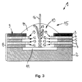
- Fig.3
- eine Darstellung ähnlich Fig.2, wobei jedoch der in das Bump-Material eingreifende Endbereich des Kontaktstifts profiliert ist.
- Fig. 1
- 2 shows a longitudinal section through a micromechanical layer arrangement, with a recess embedded in the surface of a layer stack, in which a bump for a flip-chip connection is arranged,
- Fig. 2
- a representation similar to Figure 1, but with a contact pin is embedded in the bump material and
- Fig. 3
- a representation similar to Figure 2, but the end of the contact pin engaging in the bump material is profiled.
Bei einem Verfahren zum Herstellen einer im ganzen mit 1
bezeichneten Schichtanordnung werden auf einem Substratmaterial
2, das beispielsweise aus Silizium, Galliumarsenid, Siliziumkarbid,
Indiumphospid oder dergleichen Festkörpermaterial bestehen kann,
mehrere Schichten 3, 4, 5, 6, 7 aus Festkörpermaterial zu einem
Schichtstapel 8 geschichtet. Die einzelnen Schichten 3, 4, 5, 6,
7 werden mit aus der Planartechnik an sich bekannten Verfahren,
zum Beispiel durch Sputtern oder chemical Vapour deposition (CVD),
planar auf das Substratmaterial 2 aufgebracht.In a method of manufacturing a whole with 1
designated layer arrangement are on a
Nach Fertigstellung des Schichtstapels 8 wird mittels eines
Ätzmittels in die flachseitige Oberfläche 9 des Schichtstapels 8
quer zu den Schichtungsebenen der Schichten 3, 4, 5, 6, 7 eine von
den Schichten 3, 4, 5, 6, 7 seitlich umgrenzte Ausnehmung 10
eingebracht, die mehrere der Schichten 3, 4, 5, 6, 7 durchsetzt
und an ihrer tiefsten Stelle an eine Basis-Schicht 11 angrenzt,
die in das Substratmaterial 2 eingelassen ist. An der seitlichen
Begrenzungswand der Ausnehmung 10 wird durch Abtragen von
Schichtmaterial unterschiedlicher Schichten 3, 4, 5, 6, 7 des
Schichtstapels 8 eine Profilierung erzeugt, die ausgehend von der
Oberfläche 9 des Schichtstapels 8 zum Inneren der Ausnehmung 10
hin schichtweise zwei Rücksprünge 12 und einen dazwischen
befindlichen Vorsprung 13 aufweist.After completion of the
Nach dem Fertigstellen der Profilierung wird ein flüssiges oder
fließfähiges Bump-Material 14, das beispielsweise ein Polymer oder
ein lötfähiges Metall sein kann, in die Ausnehmung 10 eingefüllt,
derart, daß es die Rücksprünge 12 hintergreift. Anschließend wird
das Bump-Material 14 verfestigt. Bei einem Polymer kann dies
beispielsweise durch Aushärten, bei einem in einem Lösungsmittel
gelösten Bump-Material durch Verdunsten des Lösungsmittels und bei
einem Metall durch Abkühlen und Erstarren erreicht werden. Nach
dem Verfestigen des Bump-Materials ergibt sich zwischen dem
Schichtstapel 8 und dem Bump-Material 14 eine formschlüssige
Verbindung, die eine hohe mechanische Festigkeit gegen Herauslösen
des Bump-Materials 1 4 aus der Ausnehmung 1 0 aufweist. Die Ausnehmung
10 wird in einem Arbeitsgang vollständig mit dem Bump-Material 14
gefüllt. Nach dem Verfestigen des Bump-Materials ist dieses deshalb
durchgehend einstückig und unter Vermeidung von Grenzschichten
miteinander verbunden.After completing the profiling, a liquid or
Das Bump-Material 14 wird derart in die Ausnehmung 10 eingefüllt,
daß es zumindest nach dem Verfestigen einen gegenüber der durch
den Umfangsrand des Bumps aufgespannten Ebene etwa in Erstreckungsrichtung
des Bumps vorstehenden Überstand 15 aufweist. Bei den in
Fig.1 bis 3 gezeigten Ausführungsbeispielen steht der Überstand
15 jeweils über die Oberfläche 9 des Schichtstapels 8 über. Der
Überstand 15 kann aber auch ganz oder teilweise im Inneren der
Ausnehmung 10 angeordnet sein. Die quer zu den Schichtungsebenen
der Schichten 3, 4, 5, 6, 7 orientierte Dicke des Überstands 14
beträgt ein Vielfaches der entsprechenden Dicke der einzelnen
Schichten 3, 4, 5, 6, 7. Der Überstand 15 kann mit einem in der
Zeichnug nicht dargestellten Verbindungsteil, beispielsweise einem
Chip, einer Leiterplatte oder einem mikromechanischen Bauteil
verbunden werden, beispielsweise durch Kleben oder Löten.The
Der Rücksprung 12 und der Vorsprung 13 werden durch Ätzen in die
Begrenzungswand der Ausnehmung 10 eingebracht. Zueinander benachbart
aneinander angrenzende Schichten 3, 5, 6, 7 des Schichtstapels 8
weisen dazu bezüglich des Ätzmittels jeweils eine unterschiedliche
Ätzrate auf. In der Zeichnung ist deutlich erkennbar, daß die
Schichten 4 und 6 etwa die gleiche Ätzrate aufweisen und daß die
dazu benachbarten Schichten 3, 5 und 7 eine größere Ätzrate haben
als die Schichten 4 und 6. Dementsprechend weist die Ausnehmung
10 im Bereich der Schichten 3, 5, 6 einen größeren Durchmesser auf
als im Bereich der Schichten 4 und 6.The
Die Schichten 4, 5, 6, 7 und die Basis-Schicht 11 bestehen aus einem
elektrisch leitfähigen, metallischem Material. Der in die Ausnehmung
10 eingreifende Bump ist als elektrischer Anschlußkontakt ausgebildet
und besteht ebenfalls aus einem elektrisch leitfähigen Material,
beispielsweise aus Metall oder einem Metallpartikel enthaltenden
Polymer-Material. Die an die Oberfläche 9 des Schichtstapels 8
angrenzende Schicht 3 ist eine elektrisch isolierende Passivierungsschicht.
Die Schichten 4, 5, 6, 7 sind jeweils an der seitlichen
Begrenzungswand der Ausnehmung 10 und die Basis-Schicht 11 ist am
Grund der Ausnehmung 10 elektrisch leitfähig mit dem Bump-Material
14 verbunden. Außerdem sind die Schichten 4, 5, 6, 7 und 11
untereinander elektrisch leitend verbunden. In vorteilhafter Weise
ergibt sich dadurch ein vergleichsweise kleiner elektrischer
Kontaktwiderstand zwischen dem Bump-Material 14 und den Schichten
4, 5, 6, 7, 11 des Schichtstapels 8. In der Zeichnung ist deutlich
erkennbar, daß durch die Rücksprünge 12 und die Vorsprünge 13 eine
relativ große Verbindungsfläche zwischen dem Bump-Material 14 und
dem Schichtstapel 8 vorhanden ist, wodurch der elektrische Widerstand
zwischen dem Bump-Material und den elektrisch leitfähigen Schichten
4, 5, 6, 7, 11 des Schichtstapels 8 zusätzlich vermindert wird.
Entsprechend ergibt sich auch eine gute Wärmeleitfähigkeit zwischen
dem Bump-Material und den Schichtstapel 8, wodurch die thermische
Beanspruchung der Schichtanordnung 1 reduziert wird.The
Bei dem Ausführungsbeispiel nach Fig.2 wird vor dem Verfestigen
des in die Ausnehmung 10 eingebrachten Bump-Materials ein
Kontaktstift 16 in das Bump-Material 14 eingesetzt, der beispielsweise
ein zu einem externen Anschlußpad führender Bonddraht sein
kann. Aus Fig.2 ist erkennbar, daß der Kontaktstift 16 mit seiner
Längsachse quer, insbesondere etwa orthogonal zu den Schichtungsebenen
der Schichten 3, 4, 5, 6, 7 angeordnet ist. Die Bondverbindung
beansprucht deshalb nur einen relativ kleinen Teilbereich der
Oberfläche 9 des Schichtstapels 8. Zum Verankern des Kontaktstift
16 in dem Bump-Material 14 kann der Kontaktstift 16 quer zu seiner
Erstreckungsrichtung orientierte Profilierungsvorsprünge 17
aufweisen, welche das Bump-Material 14 in Gebrauchsstellung jeweils
hintergreift (Fig. 3). Die Vorsprünge 17 sind zumindest an einem
in das Bump-Material eingreifenden Abschnitt des Kontaktstifts 16
vorgesehen, können aber auch in einem außerhalb des Bump-Materials
14 befindlichen Kontaktstift-Abschnitt angeordnet sein.In the embodiment of Figure 2 is before solidification
of the bump material introduced into the
Erwähnt werden soll noch, daß der Schichtstapel 8 insbesondere
zwischen zwei elektrisch leitfähigen Schichten 2, 3, 4, 5, 6, 7,
11 wenigstens eine elektrische Isolationsschicht aufweisen kann,
die zum Beispiel aus Siliziumoxyd, Siliziumnitrid oder SIPOS bestehen
kann. Bei dem Ausführungsbeispiel nach Fig.1 kann können beispielsweise
die Schichten 5, 7 Isolationsschichten sein. Solche
Isolationsschichten sind vor allem bei einem mittels eines CMOS-Prozeß
hergestellten CMOS-Bauteil von Vorteil, bei dem für die
Funktion des CMOS-Bauteils benötigte Leiterbahnen durch ganzflächiges
Aufbringen einer Metallisierung auf einen Chip und anschließendes
Maskieren dieser Metallisierung hergestellt werden, wobei zwischen
zueinander benachbarten Schichten mit Leiterbahnen jeweils eine
Isolationsschicht angeordnet wird. Die an die Ausnehmung 10 seitlich
angrenzenden Schichten 3, 4, 5, 6, 7 des Schichtstapels 8 können
dann beim Maskieren der Metallisierung in einem Arbeitsgang mit
den Leiterbahnen hergestellt werden. In vorteilhafter Weise kann
dadurch das Aufbringen zusätzlicher Schichten 3, 4, 5, 6, 7 für
den Schichtstapel 8 entfallen.It should also be mentioned that the
Zusammenfassend werden somit bei einem Verfahren zum Herstellen
einer einen Bump für eine Flip-Chip- oder dergleichen Verbindung
aufweisenden Schichtanordnung 1 mehrere Schichten 2, 3, 4, 5, 6, 7,
11 aus Festkörpermaterial zu einem Schichtstapel 8 geschichtet.
In den Schichtstapel 8 wird quer zu den Schichtungsebenen der
Schichten 2, 3, 4, 5, 6, 7, 11 eine sich über mehrere der Schichten
2, 3, 4, 5, 6, 7, 11 erstreckende Ausnehmung 10 eingebracht. In
die Ausnehmung 10 wird ein Bump-Material 14 eingebracht. An der
seitlichen Begrenzungswand der Ausnehmung 10 durch Abtragen von
Schichtmaterial unterschiedlicher Schichten 2, 3, 4, 5, 6, 7, 11
des Schichtstapels 8 eine Profilierung erzeugt wird, die ausgehend
von der Oberfläche 9 des Schichtstapels 8 zum Inneren der Ausnehmung
10 hin schichtweise wenigstens zwei Rücksprünge 12 und zumindest
einen dazwischen befindlichen Vorsprung 13 aufweist. Nach dem
Fertigstellen der Profilierung wird ein Bump-Material 14 in die
Ausnehmung 10 eingebracht, das die Rücksprünge 12 hintergreift.In summary, therefore, in a manufacturing process
one a bump for a flip-chip or the like connection
layer arrangement 1 having a plurality of
Claims (16)
Applications Claiming Priority (2)
| Application Number | Priority Date | Filing Date | Title |
|---|---|---|---|
| DE19907168 | 1999-02-19 | ||
| DE19907168A DE19907168C1 (en) | 1999-02-19 | 1999-02-19 | Layer arrangement and method for its production |
Publications (2)
| Publication Number | Publication Date |
|---|---|
| EP1030359A2 true EP1030359A2 (en) | 2000-08-23 |
| EP1030359A3 EP1030359A3 (en) | 2002-08-21 |
Family
ID=7898166
Family Applications (1)
| Application Number | Title | Priority Date | Filing Date |
|---|---|---|---|
| EP99125339A Withdrawn EP1030359A3 (en) | 1999-02-19 | 1999-12-20 | Layered structure and method of making it |
Country Status (4)
| Country | Link |
|---|---|
| US (1) | US6191489B1 (en) |
| EP (1) | EP1030359A3 (en) |
| JP (1) | JP2000243776A (en) |
| DE (1) | DE19907168C1 (en) |
Families Citing this family (13)
| Publication number | Priority date | Publication date | Assignee | Title |
|---|---|---|---|---|
| DE19852967B4 (en) * | 1998-11-17 | 2004-05-27 | Micronas Gmbh | Measuring device with a semiconductor arrangement |
| US6569753B1 (en) * | 2000-06-08 | 2003-05-27 | Micron Technology, Inc. | Collar positionable about a periphery of a contact pad and around a conductive structure secured to the contact pads, semiconductor device components including same, and methods for fabricating same |
| US7228177B2 (en) * | 2005-04-26 | 2007-06-05 | Medtronic, Inc. | Chip level biostable interconnect for implantable medical devices |
| US8575018B2 (en) * | 2006-02-07 | 2013-11-05 | Stats Chippac, Ltd. | Semiconductor device and method of forming bump structure with multi-layer UBM around bump formation area |
| KR100850763B1 (en) * | 2007-06-18 | 2008-08-06 | 삼성전기주식회사 | Printed circuit board and manufacturing method thereof |
| FR2928491A1 (en) * | 2008-03-06 | 2009-09-11 | Commissariat Energie Atomique | METHOD AND DEVICE FOR MANUFACTURING AN ASSEMBLY OF AT LEAST TWO MICROELECTRONIC CHIPS |
| US8319344B2 (en) | 2008-07-14 | 2012-11-27 | Infineon Technologies Ag | Electrical device with protruding contact elements and overhang regions over a cavity |
| US8309396B2 (en) | 2009-01-26 | 2012-11-13 | Taiwan Semiconductor Manufacturing Company, Ltd. | System and method for 3D integrated circuit stacking |
| TWI367697B (en) * | 2009-08-17 | 2012-07-01 | Nan Ya Printed Circuit Board | Printed circuit board and fabrication method thereof |
| JP5675443B2 (en) * | 2011-03-04 | 2015-02-25 | 新光電気工業株式会社 | Wiring board and method of manufacturing wiring board |
| DE102011118930A1 (en) * | 2011-11-21 | 2013-05-23 | Micronas Gmbh | Semiconductor gas sensor |
| DE102011119957A1 (en) * | 2011-12-02 | 2013-06-06 | Micronas Gmbh | fastening device |
| US10622324B2 (en) * | 2018-02-08 | 2020-04-14 | Sensors Unlimited, Inc. | Bump structures for high density flip chip interconnection |
Citations (4)
| Publication number | Priority date | Publication date | Assignee | Title |
|---|---|---|---|---|
| EP0702404A2 (en) | 1994-09-14 | 1996-03-20 | Nec Corporation | Semiconductor device |
| US5543586A (en) | 1994-03-11 | 1996-08-06 | The Panda Project | Apparatus having inner layers supporting surface-mount components |
| US5851923A (en) | 1996-01-18 | 1998-12-22 | Micron Technology, Inc. | Integrated circuit and method for forming and integrated circuit |
| US5969424A (en) | 1997-03-19 | 1999-10-19 | Fujitsu Limited | Semiconductor device with pad structure |
Family Cites Families (24)
| Publication number | Priority date | Publication date | Assignee | Title |
|---|---|---|---|---|
| JPS5844780A (en) * | 1981-09-10 | 1983-03-15 | Fujitsu Ltd | Semiconductor light emitting element |
| US4764801A (en) * | 1985-10-08 | 1988-08-16 | Motorola Inc. | Poly-sidewall contact transistors |
| US6043563A (en) * | 1997-05-06 | 2000-03-28 | Formfactor, Inc. | Electronic components with terminals and spring contact elements extending from areas which are remote from the terminals |
| EP0483408B1 (en) * | 1990-11-02 | 1995-02-08 | International Business Machines Corporation | Removable VLSI package |
| JP2644079B2 (en) * | 1990-11-05 | 1997-08-25 | 山形日本電気株式会社 | Semiconductor integrated circuit |
| JPH04188836A (en) * | 1990-11-22 | 1992-07-07 | Nippon Steel Corp | Structure of bump of semiconductor device |
| US5246880A (en) * | 1992-04-27 | 1993-09-21 | Eastman Kodak Company | Method for creating substrate electrodes for flip chip and other applications |
| US5854534A (en) * | 1992-08-05 | 1998-12-29 | Fujitsu Limited | Controlled impedence interposer substrate |
| US5262352A (en) * | 1992-08-31 | 1993-11-16 | Motorola, Inc. | Method for forming an interconnection structure for conductive layers |
| KR950001962A (en) * | 1993-06-30 | 1995-01-04 | 김광호 | Semiconductor chip bump |
| US5416872A (en) * | 1993-07-06 | 1995-05-16 | At&T Corp. | Arrangement for interconnecting an optical fiber an optoelectronic component |
| US5432675A (en) * | 1993-11-15 | 1995-07-11 | Fujitsu Limited | Multi-chip module having thermal contacts |
| US5605856A (en) * | 1995-03-14 | 1997-02-25 | University Of North Carolina | Method for designing an electronic integrated circuit with optical inputs and outputs |
| JP3183190B2 (en) * | 1995-12-14 | 2001-07-03 | 株式会社デンソー | Method for manufacturing semiconductor device |
| JPH09260529A (en) * | 1996-03-22 | 1997-10-03 | Shinko Electric Ind Co Ltd | Substrate for semiconductor device, and semiconductor device |
| KR100216839B1 (en) * | 1996-04-01 | 1999-09-01 | 김규현 | Solder ball land structure of bga semiconductor package |
| JPH09298252A (en) * | 1996-05-01 | 1997-11-18 | Shinko Electric Ind Co Ltd | Semiconductor package and semiconductor device using the semiconductor package |
| US6037786A (en) * | 1996-12-13 | 2000-03-14 | International Business Machines Corporation | Testing integrated circuit chips |
| JP3340350B2 (en) * | 1997-04-18 | 2002-11-05 | 富士通株式会社 | Thin film multilayer substrate and electronic device |
| US6117299A (en) * | 1997-05-09 | 2000-09-12 | Mcnc | Methods of electroplating solder bumps of uniform height on integrated circuit substrates |
| JPH11121897A (en) * | 1997-10-14 | 1999-04-30 | Fujitsu Ltd | Structure and production of printed wiring board mounting a plurality of circuit elements |
| US6107109A (en) * | 1997-12-18 | 2000-08-22 | Micron Technology, Inc. | Method for fabricating a semiconductor interconnect with laser machined electrical paths through substrate |
| JP2958871B2 (en) | 1998-01-07 | 1999-10-06 | カシオ計算機株式会社 | Method for manufacturing semiconductor device |
| US5955781A (en) * | 1998-01-13 | 1999-09-21 | International Business Machines Corporation | Embedded thermal conductors for semiconductor chips |
-
1999
- 1999-02-19 DE DE19907168A patent/DE19907168C1/en not_active Expired - Fee Related
- 1999-12-20 EP EP99125339A patent/EP1030359A3/en not_active Withdrawn
-
2000
- 2000-02-16 JP JP2000038351A patent/JP2000243776A/en active Pending
- 2000-02-18 US US09/506,634 patent/US6191489B1/en not_active Expired - Lifetime
Patent Citations (4)
| Publication number | Priority date | Publication date | Assignee | Title |
|---|---|---|---|---|
| US5543586A (en) | 1994-03-11 | 1996-08-06 | The Panda Project | Apparatus having inner layers supporting surface-mount components |
| EP0702404A2 (en) | 1994-09-14 | 1996-03-20 | Nec Corporation | Semiconductor device |
| US5851923A (en) | 1996-01-18 | 1998-12-22 | Micron Technology, Inc. | Integrated circuit and method for forming and integrated circuit |
| US5969424A (en) | 1997-03-19 | 1999-10-19 | Fujitsu Limited | Semiconductor device with pad structure |
Also Published As
| Publication number | Publication date |
|---|---|
| JP2000243776A (en) | 2000-09-08 |
| DE19907168C1 (en) | 2000-08-10 |
| EP1030359A3 (en) | 2002-08-21 |
| US6191489B1 (en) | 2001-02-20 |
Similar Documents
| Publication | Publication Date | Title |
|---|---|---|
| DE60011702T2 (en) | Method and structure for connecting layers in a semiconductor device | |
| DE102008028072B4 (en) | Method of manufacturing semiconductor devices | |
| DE102006021959B4 (en) | Power semiconductor device and method for its production | |
| DE19781558B4 (en) | Circuit component for an IC package and method of manufacturing the same | |
| DE10205026C1 (en) | Semiconductor substrate used for vertical integration of integrated circuits comprises a first conductor strip on its front side, and a region formed by insulating trenches and electrically insulated from the substrate | |
| DE2247902A1 (en) | Printed circuit board and process for making same | |
| DE19907168C1 (en) | Layer arrangement and method for its production | |
| DE102005049575A1 (en) | Semiconductor device with aluminum electrode and metal electrode | |
| DE102004041088B4 (en) | Semiconductor component in flat conductor technology with a semiconductor chip and method for its production | |
| DE102008058003B4 (en) | Method for producing a semiconductor module and semiconductor module | |
| DE102004047522B3 (en) | Semiconductor chip having a metal coating structure and method of making the same | |
| DE102015214228A1 (en) | Method for producing a component and a component | |
| WO2000003571A1 (en) | Method for producing interconnections with electrically conductive cross connections between the top and the bottom part of a substrate and interconnections having such cross connections | |
| WO2004073013A2 (en) | Electronic component comprising a semiconductor chip and method for producing said component | |
| DE10302022B4 (en) | Method for producing a reduced chip package | |
| DE102012206289B4 (en) | Semiconductor device composite structure with heat dissipation structure and associated manufacturing method | |
| DE10333840B4 (en) | Semiconductor component with a plastic housing, which has a Umverdrahrungsstruktur and method for their preparation | |
| DE102004044179B4 (en) | Method for mounting semiconductor chips | |
| WO2008040307A2 (en) | Method for producing an arrangement of optoelectronic components, and arrangement of optoelectronic components | |
| WO2008009347A1 (en) | Temperature sensor, and method for the production thereof | |
| DE102007002807B4 (en) | chip system | |
| DE102005057256A1 (en) | A method of manufacturing a module having an integrated circuit on a substrate and a module manufactured thereby | |
| EP0090820A1 (en) | Thin layered electronic circuit and manufacturing method thereof. | |
| DE102004030800B4 (en) | Process for producing a ceramic printed circuit board | |
| DE10359217A1 (en) | Electrical via of HL-chips |
Legal Events
| Date | Code | Title | Description |
|---|---|---|---|
| PUAI | Public reference made under article 153(3) epc to a published international application that has entered the european phase |
Free format text: ORIGINAL CODE: 0009012 |
|
| AK | Designated contracting states |
Kind code of ref document: A2 Designated state(s): AT BE CH CY DE DK ES FI FR GB GR IE IT LI LU MC NL PT SE |
|
| AX | Request for extension of the european patent |
Free format text: AL;LT;LV;MK;RO;SI |
|
| PUAL | Search report despatched |
Free format text: ORIGINAL CODE: 0009013 |
|
| AK | Designated contracting states |
Kind code of ref document: A3 Designated state(s): AT BE CH CY DE DK ES FI FR GB GR IE IT LI LU MC NL PT SE |
|
| AX | Request for extension of the european patent |
Free format text: AL;LT;LV;MK;RO;SI |
|
| 17P | Request for examination filed |
Effective date: 20020904 |
|
| AKX | Designation fees paid |
Designated state(s): DE FR GB IT NL |
|
| 17Q | First examination report despatched |
Effective date: 20070117 |
|
| STAA | Information on the status of an ep patent application or granted ep patent |
Free format text: STATUS: THE APPLICATION IS DEEMED TO BE WITHDRAWN |
|
| 18D | Application deemed to be withdrawn |
Effective date: 20140701 |