EP0986104A1 - Method of manufacturing three-dimensional device - Google Patents
Method of manufacturing three-dimensional device Download PDFInfo
- Publication number
- EP0986104A1 EP0986104A1 EP99903937A EP99903937A EP0986104A1 EP 0986104 A1 EP0986104 A1 EP 0986104A1 EP 99903937 A EP99903937 A EP 99903937A EP 99903937 A EP99903937 A EP 99903937A EP 0986104 A1 EP0986104 A1 EP 0986104A1
- Authority
- EP
- European Patent Office
- Prior art keywords
- layer
- thin film
- transferred
- making
- substrate
- Prior art date
- Legal status (The legal status is an assumption and is not a legal conclusion. Google has not performed a legal analysis and makes no representation as to the accuracy of the status listed.)
- Ceased
Links
Images


Classifications
-
- H—ELECTRICITY
- H01—ELECTRIC ELEMENTS
- H01L—SEMICONDUCTOR DEVICES NOT COVERED BY CLASS H10
- H01L27/00—Devices consisting of a plurality of semiconductor or other solid-state components formed in or on a common substrate
-
- H—ELECTRICITY
- H01—ELECTRIC ELEMENTS
- H01L—SEMICONDUCTOR DEVICES NOT COVERED BY CLASS H10
- H01L21/00—Processes or apparatus adapted for the manufacture or treatment of semiconductor or solid state devices or of parts thereof
-
- H—ELECTRICITY
- H01—ELECTRIC ELEMENTS
- H01L—SEMICONDUCTOR DEVICES NOT COVERED BY CLASS H10
- H01L23/00—Details of semiconductor or other solid state devices
- H01L23/48—Arrangements for conducting electric current to or from the solid state body in operation, e.g. leads, terminal arrangements ; Selection of materials therefor
-
- H—ELECTRICITY
- H01—ELECTRIC ELEMENTS
- H01L—SEMICONDUCTOR DEVICES NOT COVERED BY CLASS H10
- H01L27/00—Devices consisting of a plurality of semiconductor or other solid-state components formed in or on a common substrate
- H01L27/02—Devices consisting of a plurality of semiconductor or other solid-state components formed in or on a common substrate including semiconductor components specially adapted for rectifying, oscillating, amplifying or switching and having at least one potential-jump barrier or surface barrier; including integrated passive circuit elements with at least one potential-jump barrier or surface barrier
- H01L27/04—Devices consisting of a plurality of semiconductor or other solid-state components formed in or on a common substrate including semiconductor components specially adapted for rectifying, oscillating, amplifying or switching and having at least one potential-jump barrier or surface barrier; including integrated passive circuit elements with at least one potential-jump barrier or surface barrier the substrate being a semiconductor body
- H01L27/06—Devices consisting of a plurality of semiconductor or other solid-state components formed in or on a common substrate including semiconductor components specially adapted for rectifying, oscillating, amplifying or switching and having at least one potential-jump barrier or surface barrier; including integrated passive circuit elements with at least one potential-jump barrier or surface barrier the substrate being a semiconductor body including a plurality of individual components in a non-repetitive configuration
- H01L27/0688—Integrated circuits having a three-dimensional layout
-
- H—ELECTRICITY
- H01—ELECTRIC ELEMENTS
- H01L—SEMICONDUCTOR DEVICES NOT COVERED BY CLASS H10
- H01L2221/00—Processes or apparatus adapted for the manufacture or treatment of semiconductor or solid state devices or of parts thereof covered by H01L21/00
- H01L2221/67—Apparatus for handling semiconductor or electric solid state devices during manufacture or treatment thereof; Apparatus for handling wafers during manufacture or treatment of semiconductor or electric solid state devices or components; Apparatus not specifically provided for elsewhere
- H01L2221/683—Apparatus for handling semiconductor or electric solid state devices during manufacture or treatment thereof; Apparatus for handling wafers during manufacture or treatment of semiconductor or electric solid state devices or components; Apparatus not specifically provided for elsewhere for supporting or gripping
- H01L2221/68304—Apparatus for handling semiconductor or electric solid state devices during manufacture or treatment thereof; Apparatus for handling wafers during manufacture or treatment of semiconductor or electric solid state devices or components; Apparatus not specifically provided for elsewhere for supporting or gripping using temporarily an auxiliary support
- H01L2221/68359—Apparatus for handling semiconductor or electric solid state devices during manufacture or treatment thereof; Apparatus for handling wafers during manufacture or treatment of semiconductor or electric solid state devices or components; Apparatus not specifically provided for elsewhere for supporting or gripping using temporarily an auxiliary support used as a support during manufacture of interconnect decals or build up layers
-
- H—ELECTRICITY
- H01—ELECTRIC ELEMENTS
- H01L—SEMICONDUCTOR DEVICES NOT COVERED BY CLASS H10
- H01L2221/00—Processes or apparatus adapted for the manufacture or treatment of semiconductor or solid state devices or of parts thereof covered by H01L21/00
- H01L2221/67—Apparatus for handling semiconductor or electric solid state devices during manufacture or treatment thereof; Apparatus for handling wafers during manufacture or treatment of semiconductor or electric solid state devices or components; Apparatus not specifically provided for elsewhere
- H01L2221/683—Apparatus for handling semiconductor or electric solid state devices during manufacture or treatment thereof; Apparatus for handling wafers during manufacture or treatment of semiconductor or electric solid state devices or components; Apparatus not specifically provided for elsewhere for supporting or gripping
- H01L2221/68304—Apparatus for handling semiconductor or electric solid state devices during manufacture or treatment thereof; Apparatus for handling wafers during manufacture or treatment of semiconductor or electric solid state devices or components; Apparatus not specifically provided for elsewhere for supporting or gripping using temporarily an auxiliary support
- H01L2221/68368—Apparatus for handling semiconductor or electric solid state devices during manufacture or treatment thereof; Apparatus for handling wafers during manufacture or treatment of semiconductor or electric solid state devices or components; Apparatus not specifically provided for elsewhere for supporting or gripping using temporarily an auxiliary support used in a transfer process involving at least two transfer steps, i.e. including an intermediate handle substrate
-
- H—ELECTRICITY
- H01—ELECTRIC ELEMENTS
- H01L—SEMICONDUCTOR DEVICES NOT COVERED BY CLASS H10
- H01L2924/00—Indexing scheme for arrangements or methods for connecting or disconnecting semiconductor or solid-state bodies as covered by H01L24/00
- H01L2924/0001—Technical content checked by a classifier
- H01L2924/0002—Not covered by any one of groups H01L24/00, H01L24/00 and H01L2224/00
-
- H—ELECTRICITY
- H01—ELECTRIC ELEMENTS
- H01L—SEMICONDUCTOR DEVICES NOT COVERED BY CLASS H10
- H01L2924/00—Indexing scheme for arrangements or methods for connecting or disconnecting semiconductor or solid-state bodies as covered by H01L24/00
- H01L2924/10—Details of semiconductor or other solid state devices to be connected
- H01L2924/11—Device type
- H01L2924/12—Passive devices, e.g. 2 terminal devices
- H01L2924/1204—Optical Diode
- H01L2924/12044—OLED
Definitions
- the present invention relates to a method for making a three-dimensional device.
- a first layer including field effect transistors (FETs) is formed on a Si substrate by multiple steps.
- FETs field effect transistors
- a similar second layer is formed on the first layer.
- a third layer and the subsequent layers are then similarly formed thereon.
- these layers are formed on a substrate constituting a device.
- the substrate used must have adaptability as a substrate for a device and adaptability as a substrate for forming these layers. Since usable substrates are limited, the methods are disadvantageous.
- three-dimensional devices such as three-dimensional ICs have not been actually used.
- a plurality of layers is deposited using a "transfer process (transfer technology) for a thin film structure" (described later) to make a three-dimensional device, for example, a three-dimensional IC.
- a transfer process transfer technology
- a thin film structure a three-dimensional device, for example, a three-dimensional IC.
- Figs. 1 to 8 are cross-sectional views of the steps in an embodiment of a transfer process for a thin film structure in accordance with the present invention. The steps of the transfer process (cleaving method) will be described based on these drawings.
- the cleaving layer 2 adhered to the substrate 1 is also removed.
- the substrate 1 is composed of an expensive or rare material, such as quartz glass
- the substrate 1 is preferably reused or recycled.
- the present invention is applicable to the substrate 1 for which reuse is preferable, and thus is very useful.
- the transfer of the transferred layer 4 onto the member 6 is completed by the above steps.
- the intermediate layer 3 adjoining the transferred layer 4 may be removed or any other layer may be formed thereon.
- the transferred layer 4 as the cleaved member is not directly cleaved but the cleaving layer 2 bonded to the transferred layer 4 is cleaved.
- the cleaving layer 2 can be readily, securely, and uniformly cleaved or transferred regardless of the properties of the cleaved member (transferred layer 4) and the conditions. Since the cleaved member (transferred layer 4) is not damaged during the cleaving operation, the transferred layer 4 can maintain high reliability.
- the illuminating light 7 is incident on the substrate 1.
- the side away from the substrate 1 may be irradiated with the illuminating light 7, without limiting the direction of the illuminating light 7.
- the cleaving layer 2 may be partly irradiated with the illuminating light along the plane thereof, that is, with light having a given pattern so that the transferred layer 4 having the pattern is transferred (first method).
- the light incident side 12 of the substrate 1 is subjected to masking corresponding to the pattern before irradiation of the illuminating light 7 in the step ⁇ 5 ⁇ , or the positions irradiated with the illuminating light 7 are precisely controlled.
- a cleaving layer 2 having a predetermined pattern can be formed (second method) instead of the formation of the cleaving layer 2 on the entire cleaving layer forming face 11.
- a cleaving layer 2 having the predetermined pattern is previously formed by masking or the like, or the cleaving layer 2 formed on the entire cleaving layer forming face 11 is patterned or trimmed by etching or the like.
- the transfer of the transferred layer 4 can be simultaneously achieved together with the patterning and trimming.
- Transfer operations may be repeated two or more times by the above procedure.
- the transfer operations are repeated an even number of times, the relationship of the front-back of the transferred layer formed on the last member onto which the transferred layer is transferred is the same as that of the transferred layer originally formed on the substrate 1.
- Transferred layers 4 having a small unit formed on a small substrate 1 having, for example, an effective area of 45 mm ⁇ 40 mm can be sequentially transferred onto the adjacent positions of a large transparent substrate having, for example, an effective area of 900 mm ⁇ 1,600 mm a plurality of times (for example, approximately 800 times) to form the transferred layer 4 onto the entire effective area of the large transparent substrate).
- a liquid crystal display having the same size as that of the large transparent substrate can be thereby produced.
- a plurality of transferred layers 4 formed on the substrates 1 may be sequentially transferred (overlapped) onto the member 6 to form a composite of the transferred layers 4.
- the transferred layers 4 to be overlapped may be the same or different.
- a first embodiment of a method for making a three-dimensional device (multilayered device) using the above-mentioned method for transferring a thin film configuration will now be described.
- Fig. 9 is a schematic cross-sectional view of a configuration of a three-dimensional device
- Figs. 10 to 15 are schematic cross-sectional views of the steps in the first embodiment of a method for making a three-dimensional device in accordance with the present invention.
- the common points with the above-described transfer process of the thin film configuration will not be described.
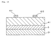
- a three-dimensional device 10 has a substrate (transferring-side substrate) 21 as a base, a first transferred layer (first thin film device layer) 41, and a second transferred layer (second thin film device layer) 42.
- the transferred layers 41 and 42 extend two-dimensionally (parallel to the substrate 21) to form a predetermined circuit.
- the transferred layer 41 is bonded on the upper side of the substrate 21 in Fig. 9 with an adhesive layer 5.
- the transferred layer 42 is bonded on the upper side of the transferred layer 41 in Fig. 9 with a conductive adhesive layer 22.
- the transferred layer 41 has connecting electrodes (connecting terminals) 411 and 412 thereon in Fig. 9.
- the transferred layer 42 has connecting electrodes (connecting terminals) 421 and 422 thereunder in Fig. 9.
- the connecting electrode 411 of the transferred layer 41 and the connecting electrode 421 of the transferred layer 42 are electrically connected to each other via the conductive adhesive layer 22, whereas the connecting electrode 412 of the transferred layer 41 and the connecting electrode 422 of the transferred layer 42 are electrically connected to each other via the conductive adhesive layer 22.
- a preferable conductive adhesive layer 22 is an anisotropic conductive film (ACF). Since bonding with the anisotropic conductive film enables conduction only in the thickness direction (the longitudinal direction in Fig. 9), short-circuiting in the transverse direction in Fig. 9 is prevented. That is, short-circuiting between the connecting electrodes 411 and 412, between the connecting electrodes 411 and 422, between the connecting electrodes 421 and 422, and between the connecting electrodes 421 and 412 is prevented.
- ACF anisotropic conductive film
- the transferred layer 41 and the transferred layer 42 are bonded to each other while the connecting electrodes 411 and 421 and the connecting electrodes 412 and 422 are aligned so as to be electrically connected.
- the substrate (transferring-side substrate) 21 of the three-dimensional device 10 corresponds to the member 6 onto which the transferred layer is transferred in Figs. 4 to 8.
- Examples of the transferred layers 41 and 42 of the three-dimensional device 10 include the above-described various types as the transferred layers 4.
- the transferred layers 41 and 42 may be dynamic RAMs (DRAMs), static RAMs (SRAMs), memories such as E 2 PROMs and ROMs, logics (logic circuits) such as CPU, and sensors such as an optical sensor or a magnetic sensor.
- DRAMs dynamic RAMs
- SRAMs static RAMs
- E 2 PROMs E 2 PROMs
- ROMs E 2 PROMs
- logics logic circuits
- CPU optical sensor
- sensors such as an optical sensor or a magnetic sensor.
- the transferred layers 41 and 42 are not limited to the above examples.
- the transferred layers 41 and 42 may be the same or different.
- the transferred layer 41 and the transferred layer 42 may be, for example, memories (memory cell arrays).
- memories memory cell arrays
- a large-capacity memory integrated memory
- the transferred layer 41 and the transferred layer 42 may be, for example, logics (logic circuits).
- a large-capacity logic (integrated logic) is thereby achieved.
- the three-dimensional device 10 is a system IC (for example, a system LSI) including (or integrating) a memory and a logic.
- the transferred layer 41 and the transferred layer 42 can be formed using different design rules (minimum line widths) according to the present invention.
- the transferred layer 41 and the transferred layer 42 can also be formed using different design parameters.
- the transferred layer 41 and the transferred layer 42 can be formed by different production processes. In conventional methods, it is impossible or difficult to change such conditions between the layers to be deposited.
- the minimum line width of the memory in the system IC is, for example, approximately 0.35 ⁇ m ( ⁇ m rule), and the minimum line width of the logic is, for example, approximately 0.5 ⁇ m ( ⁇ m rule) (the minimum line width of the memory is smaller than the minimum line width of the logic). In contrast, the minimum width of the memory may be larger than the minimum width of the logic.
- the three-dimensional device 10 is produced by the above-mentioned transfer process of a thin film configuration, for example, as follows.
- the cleaving layer 2 remaining on the substrate 1 is also removed.
- the substrate 1 is composed of an expensive or rare material, such as quartz glass
- the substrate 1 is preferably reused or recycled.
- the present invention is applicable to the substrate 1 for which reuse is preferable, and thus is very useful.
- the transfer of the transferred layer 42 onto the transferred layer 41 that is, deposition of the transferred layer 42 onto the transferred layer 41 is completed by the above steps. In the subsequent step, any other layer may be formed thereon.
- a three-dimensional device for example, a three-dimensional IC 10 can be readily produced by transfer according to the present invention.
- ICs can be formed in a relatively small area even by a relatively moderated design rule.
- each thin film device layer can be formed by appropriate device parameters, for example, a gate line width, a thickness of the gate insulating film, a design rule, and production conditions such as temperature. Since each thin film device layer can be formed by optimized device parameters, the resulting three-dimensional device 10 has high reliability and high performance.
- the three-dimensional device 10 is a system IC (for example, a system LSI) including (or integrating) a memory and a logic
- the memory and the logic can be formed by desirable processes in the production of the system IC, resulting in readily production, high productivity, and advantageous mass production.
- the three-dimensional device 10 has a three-dimensional configuration (has a three-dimensional circuit).
- the product yield is improved compared to production of three-dimensional devices by deposition of each layer on the same substrate (direct formation of each layer).
- Transfer can be performed onto various substrates 21 (transferred-side substrates) without limitation. That is, a thin film device layer can be formed by transfer onto a substrate composed of a material which is not capable of or suitable for direct formation of the thin film device layer, which can be readily shaped, or which is inexpensive. In other words, the substrate 21 is appropriately selected. Since ICs can be formed on a flexible substrate, and IC cards and the like can be readily produced.
- the transfer of the transferred layers (thin film device layers) 41 and 42 is performed once.
- the transfer of the transferred layer 41 may be performed two or more times and the transfer of the transferred layer 42 may be performed two or more times, as long as the transferred layer 41 and the transferred layer 42 can be deposited.
- the transferred layer on the substrate 1 is transferred onto a third substrate (not shown in the drawing), not onto the substrate 1 and the substrate 21, and then the transferred layer on the third substrate is transferred onto the substrate 21.
- the above-described cleaving layer 2 is previously formed on the third substrate.
- the relationship of the front-back of the transferred layer formed on the substrate (transferred-side substrate) 21 being the last member onto which the transferred layer is transferred is the same as that of the transferred layer originally formed on the substrate (original substrate) 1.
- a transferred layer 41 may be directly formed onto the substrate (transferring-side substrate) 21 and a transferred layer 42 may be transferred onto the transferred layer 41 by the above-described transfer process to produce a three-dimensional device 10.
- Three or more transferred layers may be deposited in the present invention.
- An increase in the deposited transferred layers causes an increase in integration density.
- connecting electrodes are formed at both ends of a third transferred layer (third thin film device layer) 43 disposed between a first transferred layer (first thin film device layer) 41 and a second transferred layer (second thin film device layer) 42. That is, connecting electrodes 431 and 432 are formed at one end of the transferred layer 43 (the lower side in Fig. 16), whereas connecting electrodes 433 and 434 are formed at the other end (the upper side in Fig. 16).
- the connecting electrode 411 of the transferred layer 41 and the connecting electrode 431 of the transferred layer 43 are electrically connected via a conductive adhesive layer 22, and the connecting electrode 412 of the transferred layer 41 and the connecting electrode 432 of the transferred layer 43 are electrically connected via the conductive adhesive layer 22.
- the connecting electrode 433 of the transferred layer 43 and the connecting electrode 421 of the transferred layer 42 are electrically connected via a conductive adhesive layer 23, and the connecting electrode 434 of the transferred layer 43 and the connecting electrode 422 of the transferred layer 42 are electrically connected via the conductive adhesive layer 23.
- a preferable conductive adhesive layer 23 is an anisotropic conductive film for the same reason as that for the conductive adhesive layer 22.
- these layers may be completely the same or different, or may be partially the same.
- Fig. 17 is a schematic cross-sectional view of a configuration of a three-dimensional device.
- the common points with the above-described first embodiment are not described, and main differences will be described.
- a three-dimensional device 10 shown in Fig. 17 is also produced by a transfer process of a thin film configuration as in the first embodiment.
- the connecting electrode 411 of the first transferred layer (first thin film device layer) 41 is put into contact with the connecting electrode 421 of the second transferred layer (second thin film device layer) 42 to electrically connect these layers
- the connecting electrode 412 of the transferred layer 41 is put into contact with the connecting electrode 422 of the second transferred layer 42 to electrically connect these layers
- the transferred layer 41 and the transferred layer 42 are bonded to each other with an adhesive layer 24.
- the second embodiment also has the same advantages as that of the first embodiment.
- the method for bonding the transferred layer 41 to the transferred layer 42 and the method for electrically connecting the corresponding connecting electrodes are not limited to those described in the first embodiment and the second embodiment.
- the connecting electrodes 411 and 412 are put into contact with the connecting electrodes 421 and 422, respectively, these are heated to melt the contact faces, and then the faces are solidified to bond the corresponding connecting electrodes. As a result, the corresponding connecting electrodes are electrically connected and the transferred layer 41 and the transferred layer 42 are bonded.
- solder conductive brazing agent
- a solder may be disposed between the connecting electrode 411 and the connecting electrode 421 and between the connecting electrode 412 and the connecting electrode 422, may be heated to be melted, and may then be solidified.
- the corresponding connecting electrodes are electrically connected via the solder and the transferred layer 41 and the transferred layer 42 are bonded with the solder.
- Fig. 18 is a schematic cross-sectional view of a configuration of a three-dimensional device.
- the common points with the above-described first embodiment are not described, and main differences will be described.
- a three-dimensional device 10 shown in Fig. 18 is also produced by a transfer process of a thin film configuration as in the first embodiment.
- a light emitting section (luminescent device) 413 and a light receiving section (light receiving device) 414 are formed on one face of a first transferred layer (first thin film device layer) 41 (the upper side in Fig. 18) of the three-dimensional device 10.
- a light emitting section (luminescent device) 423 and a light receiving section (light receiving device) 424 are formed on one face of a second transferred layer (second thin film device layer) 42 (the lower side in Fig. 18).
- step ⁇ A7 ⁇ positioning is performed so that the light emitting sections are opposite the corresponding light receiving section, that is, the light emitting section 413 is opposite the light receiving section 424 and the light emitting section 423 is opposite the light receiving section 414, while the transferred layer 41 and the transferred layer 42 are bonded to each other with a substantially transparent adhesive layer 25 (having transmissivity to light from the light emitting sections 413 and 423).
- organic EL devices can be used as the light emitting sections 413 and 423 in the three-dimensional device 10.
- Fig. 19 is a cross-sectional view of a configuration of an organic electroluminescent (EL) device.
- an organic EL device 30 has a barrier (bank) 34, a transparent electrode 31 and a light emitting layer (organic EL) 32 formed in the barrier 34, and a metallic electrode 33.
- the light emitting layer 32 is formed on the transparent electrode 31, and the metallic electrode 33 is formed on the barrier 34 and the light emitting layer 32.
- the transparent electrode 31 is composed of, for example, ITO.
- the light emitting layer 32 is composed of a thin film (solid thin film) obtained by heating an organic EL device composition in which a precursor of a conjugated organic polymer for forming the light emitting layer 32 and a fluorescent pigment for modifying the luminescent characteristics of the light emitting layer 32 are dissolved or dispersed into a given solvent (polar solvent) so that the precursor in the organic EL device composition is polymerized.
- a precursor of a conjugated organic polymer for forming the light emitting layer 32 and a fluorescent pigment for modifying the luminescent characteristics of the light emitting layer 32 are dissolved or dispersed into a given solvent (polar solvent) so that the precursor in the organic EL device composition is polymerized.
- the metallic electrode 33 is composed of, for example, Al-Li.
- the barrier 34 is composed of, for example, a resin black resist.
- Each of the transferred layers 41 and 42 has a driving section (driving circuit) (not shown in the drawing) for driving the organic EL device 30.
- PIN photodiodes may be used as the light receiving sections 414 and 424 in the three-dimensional device 10.
- Fig. 20 is a cross-sectional view of a configuration of a PIN photodiode.
- a PIN photodiode 50 includes a light-receiving section window electrode 51, a p-type a-SiC layer (p-type semiconductor layer) 52, an i-type a-SiC layer (i-type semiconductor layer) 53, an n-type a-SiC layer (n-type semiconductor layer) 54, and an Al-Si-Cu layer 55 functioning as a light-receiving section upper electrode and a lead line (electrical line).
- the light-receiving section window electrode 51, the p-type a-SiC layer 52, the i-type a-SiC layer 53, the n-type a-SiC layer 54, and the Al-Si-Cu layer 55 are deposited in that order from the bottom side in Fig. 20.
- the light-receiving section window electrode 51 is composed of, for example, ITO.
- the organic EL device 30 is driven by a driving circuit (not shown in the drawing) electrically connected to the organic EL device 30 to emit light. That is, the organic EL device 30 submits optical signals (light).
- the light from the organic EL device 30 passes through the adhesive layer 25 and is incident on the light-receiving section window electrode 51. That is, the PIN photodiode 50 receives the light.
- the PIN photodiode 50 outputs a current, i.e., an electrical signal in response to the intensity of the received light (the optical signal is output as an electrical signal).
- a circuit (not shown in the drawing) electrically connected to the PIN photodiode 50 operates based on the signal from the PIN photodiode 50.
- the light from the light emitting section 413 passes through the adhesive layer 25 and is incident on the light receiving section 424, and the light from the light emitting section 423 passes through the adhesive layer 25 and is incident on the light receiving section 414. That is, the light emitting sections 413 and 423 and the light receiving sections 414 and 424 perform optical communication between the transferred layer 41 and the transferred layer 42.
- the third embodiment also has the same advantages as that of the first embodiment.
- signal transmittance between layers is performed by optical signals, not by electrical signals.
- production is facilitated and integration density can be further increased.
- the light emitting sections 413 and 423 may be composed of inorganic EL devices, light emitting diodes (LEDs), or semiconductor lasers (laser diodes), in addition to the organic EL devices.
- LEDs light emitting diodes
- laser diodes semiconductor lasers
- the light receiving sections 414 and 424 may be composed of photodiodes, such as PN photodiodes and avalanche photodiodes, phototransistors, and photoluminescence devices (organic and inorganic photoluminescence devices), in addition to the PIN photodiodes.
- photodiodes such as PN photodiodes and avalanche photodiodes, phototransistors, and photoluminescence devices (organic and inorganic photoluminescence devices), in addition to the PIN photodiodes.
- the bonding method of the transferred layer (thin film device layer) 41 and the transferred layer (thin film device layer) 42 is not limited to the above-described method. That is, the transferred layer 41 and the transferred layer 42 are bonded to each other so that optical communication is achieved between the transferred layer 41 and the transferred layer 42.
- the transferred layer 41 and the transferred layer 42 can be partly bonded to each other.
- the transferred layer 41 and the transferred layer 42 may be bonded to each other with an opaque adhesive layer.
- the transferred layer 41 and the transferred layer 42 may be bonded to each other with a spacer (for example, a column) provided between the transferred layer 41 and the transferred layer 42.
- a spacer for example, a column
- gaps are formed between the light emitting section 413 and the light receiving section 414 of the transferred layer 41 and between the light emitting section 423 and the light receiving section 424 of the transferred layer 42.
- the light emitting section 413 of the transferred layer 41 may be put into contact with the light receiving section 414, and the light emitting section 424 of the transferred layer 42 may be put into contact with the light receiving section 423.
- this embodiment may include a configuration enabling optical communication between layers which are not adjacent to each other.
- the light emitting section may consist of a plurality of luminescent devices having different luminescent characteristics (for example, peak wavelengths of the luminescent light) and the light receiving section may consist of a plurality of light receiving devices for receiving the light from the corresponding luminescent devices.
- a plurality of information signals can be simultaneously transmitted. That is, information transmission by multichannel optical communication is achieved.
- a plurality of light emitting sections having different luminescent characteristics may be provided and a plurality of light receiving sections may be provided for receiving the light from the corresponding light emitting sections.
- the present invention also includes a configuration, which can achieve optical communication in at least a given transferred layer (thin film device layer), as in that between the transferred layers (thin film device layers).
- given transferred layers may be electrically connected to each other as in the first and second embodiments, whereas the other transferred layers may be optically connected to each other as in the third embodiment so as to enable optical communication.
- partial regions of given transferred layers may be electrically connected to each other and the other regions may be optically connected to each other.
- a three-dimensional device may be produced by transferring at least one layer among a plurality of transferred layers (thin film device layers) in the three-dimensional device by the above-mentioned transfer process (transfer technology) of the thin film configuration.
- the transfer process in the present invention is not limited to the above-described method.
- the three-dimensional device for example, a three-dimensional IC is readily produced.
- each thin film device layer can be formed by optimized device parameters, and the resulting device has high reliability and high performance.
- the product yield is improved compared to production of three-dimensional devices by deposition of each layer on the same substrate (direct formation of each layer).
Abstract
Description
- The present invention relates to a method for making a three-dimensional device.
- In conventional processes for making three-dimensional devices such as three-dimensional ICs, a first layer including field effect transistors (FETs) is formed on a Si substrate by multiple steps. Next, a similar second layer is formed on the first layer. A third layer and the subsequent layers are then similarly formed thereon.
- In the conventional processes for making three-dimensional devices, however, these layers are deposited on the same substrate; hence, overlying layers must be formed so as not to adversely affect the layer thereunder with various restrictions, for example, the upper temperature limit, so that the underlying layers are not affected.
- When different layers are deposited, it is very difficult to produce these layers at desired device parameters, for example, gate line width, thickness of the gate insulating film, design rule, and process conditions such as production temperature.
- In addition, in the conventional methods for making three-dimensional devices, these layers are formed on a substrate constituting a device. Thus, the substrate used must have adaptability as a substrate for a device and adaptability as a substrate for forming these layers. Since usable substrates are limited, the methods are disadvantageous.
- Accordingly, three-dimensional devices such as three-dimensional ICs have not been actually used.
- It is an object of the present invention to provide a method for making three-dimensional devices under a wide variety of forming conditions for thin film device layers and for facilitating production of high-performance three-dimensional devices.
- Such an object is achieved by the following embodiments (1) to (22) according to the present invention.
- (1) A method for making a three-dimensional device comprising depositing in the thickness direction a plurality of thin film device layers disposed in a predetermined region in the two-dimensional direction, wherein at least one of the thin film device layers is deposited by a transfer process.
- (2) A method for making a three-dimensional device
constituting a three-dimensional circuit comprising:
depositing in the thickness direction a plurality of thin
film device layers constituting a circuit in a predetermined
region in the two-dimensional direction on a substrate,
wherein at least one of the thin film device layers is deposited by a transfer process. - (3) A method for making a three-dimensional device according to the above (1) or (2), wherein the transfer process comprises forming a thin film device layer on a first substrate with a cleaving layer provided therebetween, and irradiating the cleaving layer with illuminating light so as to form cleavage in the cleaving layer and/or at the interface thereof and to transfer the thin film device layer on the first substrate onto a second substrate side.
- (4) A method for making a three-dimensional device according to the above (3), wherein the cleavage of the cleaving layer is generated by breakage or attenuation of atomic or molecular bonding force of substances constituting the cleaving layer.
- (5) A method for making a three-dimensional device according to the above (3), wherein the cleavage of the cleaving layer is generated by gas evolved from the substance constituting the cleaving layer.
- (6) A method for making a three-dimensional device according to any one of the above (3) to (5), wherein the illuminating light is laser light.
- (7) A method for making a three-dimensional device according to the above (6), wherein the wavelength of the laser light is 100 to 350 nm.
- (8) A method for making a three-dimensional device according to the above (6), wherein the wavelength of the laser light is 350 to 1,200 nm.
- (9) A method for making a three-dimensional device according to any one of the above (3) to (8), wherein the cleaving layer comprises amorphous silicon, ceramic, metal or an organic polymer.
- (10) A method for making a three-dimensional device according to any one of the above (3) to (9), wherein the first substrate is a transparent substrate.
- (11) A method for making a three-dimensional device according to any one of the above (1) to (10), wherein each of the thin film device layers is provided with connecting electrodes, and the connecting electrodes electrically connect the two adjacent thin film device layers.
- (12) A method for making a three-dimensional device according to the above (11), wherein the connecting electrodes are disposed on the two surfaces of the thin film device layer.
- (13) A method for making a three-dimensional device according to the above (11) or (12), wherein the two adjacent thin film device layers are bonded to each other with an anisotropic conductive film therebetween.
- (14) A method for making a three-dimensional device according to any one of the above (1) to (10), wherein in the two selected layers among the thin film device layers, one of the two selected layers is provided with a light emitting section and the other layer is provided with a light receiving section for receiving the light from the light emitting section, the light emitting section and the light receiving section enabling optical communication between the two layers.
- (15) A method for making a three-dimensional device according to any one of the above (1) to (14), wherein the thin film device layer deposited by the transfer is simultaneously produced with at least one of the other thin film device layers.
- (16) A method for making a three-dimensional device according to any one of the above (1) to (15), wherein at least one of the thin film device layers has a plurality of thin film transistors.
- (17) A method for making a three-dimensional device according to any one of the above (1) to (16), wherein the thin film device layers as memory are transferred a plurality of times to form a large-scale memory.
- (18) A method for making a three-dimensional device according to any one of the above (1) to (16), wherein the thin film device layers as logic are transferred a plurality of times to form a large-scale logic.
- (19) A method for making a three-dimensional device according to any one of the above (1) to (16), wherein the thin film device layers as memory and the thin film device layers as logic are transferred to form a system LSI.
- (20) A method for making a three-dimensional device according to the above (19), wherein the logic and the memory are formed by different design rules.
- (21) A method for making a three-dimensional device according to the above (19), wherein the logic and the memory are formed by different design parameters.
- (22) A method for making a three-dimensional device according to the above (19), wherein the logic and the memory are formed by different production processes.
-
-
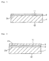
- Fig. 1 is a schematic cross-sectional view of a step in an embodiment of a transfer process of a thin film structure in accordance with the present invention.
- Fig. 2 is a schematic cross-sectional view of a step in an embodiment of a transfer process of a thin film structure in accordance with the present invention.
- Fig. 3 is a schematic cross-sectional view of a step in an embodiment of a transfer process of a thin film structure in accordance with the present invention.
- Fig. 4 is a schematic cross-sectional view of a step in an embodiment of a transfer process of a thin film structure in accordance with the present invention.
- Fig. 5 is a schematic cross-sectional view of a step in an embodiment of a transfer process of a thin film structure in accordance with the present invention.
- Fig. 6 is a schematic cross-sectional view of a step in an embodiment of a transfer process of a thin film structure in accordance with the present invention.
- Fig. 7 is a schematic cross-sectional view of a step in an embodiment of a transfer process of a thin film structure in accordance with the present invention.
- Fig. 8 is a schematic cross-sectional view of a step in an embodiment of a transfer process of a thin film structure in accordance with the present invention.
- Fig. 9 is a schematic cross-sectional view of a configuration of a three-dimensional device in accordance with the present invention.
- Fig. 10 is a schematic cross-sectional view of a step in a first embodiment of a method for making a three-dimensional device in accordance with the present invention.
- Fig. 11 is a schematic cross-sectional view of a step in a first embodiment of a method for making a three-dimensional device in accordance with the present invention.
- Fig. 12 is a schematic cross-sectional view of a step in a first embodiment of a method for making a three-dimensional device in accordance with the present invention.
- Fig. 13 is a schematic cross-sectional view of a step in a first embodiment of a method for making a three-dimensional device in accordance with the present invention.
- Fig. 14 is a schematic cross-sectional view of a step in a first embodiment of a method for making a three-dimensional device in accordance with the present invention.
- Fig. 15 is a schematic cross-sectional view of a step in a first embodiment of a method for making a three-dimensional device in accordance with the present invention.
- Fig. 16 is a schematic cross-sectional view of another configuration of a three-dimensional device in accordance with the present invention.
- Fig. 17 is a schematic cross-sectional view of another configuration of a three-dimensional device in accordance with the present invention.
- Fig. 18 is a schematic cross-sectional view of another configuration of a three-dimensional device in accordance with the present invention.
- Fig. 19 is a cross-sectional view of a configuration of an organic electroluminescent (EL) device in accordance with the present invention.
- Fig. 20 is a cross-sectional view of a configuration of a PIN photodiode in accordance with the present invention.
-
-
- 1
- substrate
- 11
- cleaving layer forming face
- 12
- light incident face
- 2
- cleaving layer
- 2a, 2b
- interface
- 3
- intermediate layer
- 4, 41 to 43
- transferred layer
- 411, 412
- connecting electrode
- 421, 422
- connecting electrode
- 413, 423
- light emitting section
- 414, 424
- light receiving section
- 431 to 424
- connecting electrode
- 5
- adhesive layer
- 6
- member onto which a transferred layer is transferred.
- 7
- illuminating light
- 10
- three-dimensional device
- 21
- substrate
- 22, 23
- conductive adhesive layer
- 24
- adhesive layer
- 25
- transparent adhesive layer
- 30
- organic EL device
- 31
- transparent electrode
- 32
- light emitting layer
- 33
- metallic electrode
- 34
- barrier
- 50
- PIN photodiode
- 51
- window electrode of light receiving section
- 52
- p-type a-SiC layer
- 53
- i-type a-SiC layer
- 54
- n-type a-SiC layer
- 55
- Al-Si-Cu layer
- 60
- thin film transistor
- 61
- source layer
- 62
- drain layer
- 63
- channel layer
- 64
- gate insulating film
- 65
- gate electrode
- 66
- insulating interlayer
- 67, 68
- electrode
- 69
- protective film
- A method for making a three-dimensional device in accordance with the present invention will now be described with reference to the preferred embodiments shown in the attached drawings.
- In the present invention, a plurality of layers is deposited using a "transfer process (transfer technology) for a thin film structure" (described later) to make a three-dimensional device, for example, a three-dimensional IC. First, the "transfer process for a thin film structure" will be described.
- Figs. 1 to 8 are cross-sectional views of the steps in an embodiment of a transfer process for a thin film structure in accordance with the present invention. The steps of the transfer process (cleaving method) will be described based on these drawings.
- 〈1〉 As shown in Fig. 1, a cleaving layer (light absorption
layer) 2 is formed on one face (cleaving layer forming face
11) of the
substrate 1. When the side of thesubstrate 1 is irradiated with illuminating light 7, thesubstrate 1 is preferably translucent so as to transmit the illuminating light 7.The transmittance of the illuminatinglight 7 is preferably 10% or more, and more preferably 50% or more. An excessively low transmittance causes large attenuation (loss) of the illuminatinglight 7, and thus a high luminous intensity is necessary for cleavage of thecleaving layer 2. Thesubstrate 1 is preferably composed of a highly reliable material, and more preferably is composed of a heat resistant material. When a transferredlayer 4 and anintermediate layer 3, which will be described below, are formed, a high process temperature (for example, 350 to 1,000°C) may be required for some types of layers and in some methods for making these layers. When thesubstrate 1 has high heat resistance, a wide variety of film deposition conditions such as temperature can be manipulated in the formation of the transferredlayer 4 on the substrate 1.When the maximum temperature during the formation of the transferredlayer 4 is Tmax, thesubstrate 1 is preferably composed of a material having a heat distortion point which is higher than the Tmax. In detail, the materials for thesubstrate 1 have a heat distortion point of preferably 350°C or more, and more preferably 500°C or more. Examples of such materials include heat resistant glasses, such as quartz glass, soda glass, Corning 7059, and Nippon Electric Glass OA-2.When thecleaving layer 2, theintermediate layer 3 and the transferredlayer 4 are formed at low process temperatures, thesubstrate 1 may be composed of an inexpensive glass or synthetic resin having a low melting point.Although the thickness of thesubstrate 1 is not limited, it is in a range of preferably 0.1 to 5.0 mm and more preferably 0.5 to 1.5 mm. An excessively small thickness of thesubstrate 1 results in decreased strength, whereas an excessively large thickness readily causes high attenuation of the illuminating light 7 when the transmittance of thesubstrate 1 is low. When thesubstrate 1 has a high transmittance for the illuminatinglight 7, the thickness may exceed the above range.The thickness of thesubstrate 1 at the position for forming the cleaving layer is preferably uniform so as to be uniformly irradiated with the illuminating light 7.The cleavinglayer forming face 11 and the light incident face 12 of thesubstrate 1 is not limited to be flat as shown in the drawing and may be curved.In the present invention, thesubstrate 1 is not removed by etching or the like, but is detached by cleavage of thecleaving layer 2 provided between thesubstrate 1 and the transferredlayer 4. Thus, the operation is easy, and various materials, for example, a material having a relatively large thickness, may be used as the substrate 1.Thecleaving layer 2 will now be described.Thecleaving layer 2 absorbs illuminating light 7 described below to cause cleavage in the layer and/or at aninterface cleaving layer 2, that is, by ablation.Furthermore, the irradiation of the illuminating light 7 will cause cleavage by gas evolved from thecleaving layer 2 in some cases. Components contained in thecleaving layer 2 will be evolved as gas in some cases, or the vapor formed by instantaneous gasification of thecleaving layer 2 by light absorption will contribute to the cleavage in some cases.The following are examples of compositions of thecleaving layer 2. - (1) Amorphous silicon (a-Si)
The amorphous silicon may contain hydrogen (H). The
hydrogen content is preferably 2 atomic percent or more, and
more preferably in a range of approximately 2 to 20 atomic
percent. When a predetermined content of hydrogen is
contained, hydrogen is evolved by irradiation of the
illuminating
light 7, and the internal pressure formed in thecleaving layer 2 yields a force inducing cleavage between the upper and lower thin films.The hydrogen content in the amorphous silicon can be controlled by the film deposition conditions, for example, the gas composition in CVD, gas pressure, gas atmosphere, gas flow rate, temperature, substrate temperature, and input power. - (2) Oxide ceramics, dielectric (ferroelectric) materials, and semiconductors, such as silicon dioxide or silicates, titanium oxide or titanates, zirconium oxide or zirconates, and lanthanum oxide or lanthanates. Examples of silicon oxide include SiO, SiO2, and Si3O2. Silicates include K2SiO3, Li2SiO3, CaSiO3, ZrSiO4, and Na2SiO3.Examples of titanium oxide include TiO, Ti2O3, and TiO2. Titanates include BaTiO4, BaTiO3, Ba2Ti9O20, Ba2Ti5O11, CaTiO3, SrTiO3, PbTiO3, MgTiO3, ZrTiO2, SnTiO4, Al2TiO5, and FeTiO3.Zirconium oxide includes ZrO2. Examples of zirconates include BaZrO3, ZrSiO4, PbZrO3, MgZrO3, and K2ZrO3.
- (3) Ceramics and dielectric materials (ferroelectric materials), such as PZT, PLZT, PLLZT, and PBZT.
- (4) Nitride ceramics, such as silicon nitride, aluminum nitride, and titanium nitride.
- (5) Organic polymers Any organic polymer may be used, as long as the polymer has bonds and particularly has many bonds, such as -CH2-, -CO- (carbonyl), -CONH- (amido), -NH- (imido), -COO- (ester), -N=N- (azo), and -CH=N- (schif) (these bonds are broken by irradiation of the illuminating light 7). The organic polymer may contain aromatic hydrocarbon groups (at least one benzene ring or fused ring) in the chemical formula.Examples of the organic polymers include polyolefins, such as polyethylene and polypropylene, polyimides, polyamides, polyesters, polymethyl methacrylate (PMMA), polyphenylene sulfide (PPS), polyether sulfones (PES), and epoxy resins.
- (6) Metals Examples of metals include aluminum, lithium, titanium, manganese, indium, tin, samarium, and alloys containing at least one of these metals. The thickness of the
- 〈2〉 As shown in Fig. 2, an intermediate layer (underlying
layer) 3 is formed on the
cleaving layer 2. Theintermediate layer 3 is formed for various purposes, for example, as at least one layer among a protective layer for physically or chemically protecting the below-mentioned transferredlayer 4, an insulating layer, a conductive layer, a shading layer for the illuminatinglight 7, a barrier layer inhibiting migration to the transferredlayer 4 or from the transferredlayer 4, and a reflective layer.The composition of theintermediate layer 3 may be determined depending on the purpose of the formation. For example, anintermediate layer 3, which is formed between an amorphoussilicon cleaving layer 2 and a thin film (TFT) transferredlayer 4, is composed of silicon oxide, such as SiO2. Anintermediate layer 3 formed between thecleaving layer 2 and a PZT transferredlayer 4 is composed of a metal, e.g., platinum, gold, tungsten, tantalum, molybdenum, aluminum, chromium, or titanium, or an alloy containing such a metal.The thickness of theintermediate layer 3 is determined depending on the purpose of the formation and the required functions. The thickness is in a range of preferably 10 nm to 5 µm and more preferably 40 nm to 1 µm.The method for forming theintermediate layer 3 may be the same as that for forming thecleaving layer 2. Theintermediate layer 3 may be formed by two or more steps.Theintermediate layer 3 includes two or more layers having the same composition or different compositions. In the present invention, the transferredlayer 4 may be directly formed on thecleaving layer 2 without forming theintermediate layer 3. - 〈3〉 As shown in Fig. 3, the transferred layer (cleaved
member) 4 is formed on the
intermediate layer 3. The transferred layer 4 is the layer which is transferred onto a member 6, described below, and may be formed by the same method for forming the cleaving layer 2.Although the purpose for the formation, the type, the shape, the configuration, the composition, and physical and chemical properties of the transferred layer 4 are not limited, it is preferably a thin film and particularly a functional thin film or a thin film device, in consideration of the purpose and usefulness of the transfer.Examples of functional thin films and thin film devices include thin film transistors (TFTs), thin film diodes, and other thin film semiconductor devices; electrodes, e.g., transparent electrodes, such as ITO and tin oxide films; photovoltaic elements used in solar cells and image sensors; switching elements, memories; actuators such as piezoelectric elements; micromirrors, e.g., thin film piezoelectric ceramics; recording media, such as magnetic recording media, magneto-optical recording media, and optical recording media; thin film magnetic recording heads, coils, inductors, thin film high-permeability materials, and magnetic microdevices by combination thereof; optical thin films, such as filters, reflective films, dichroic mirrors, and polarizing elements; semiconductor thin films; superconducting thin films, e.g., YBCO thin films; magnetic thin films; multilayered metallic thin films: multilayered metal-ceramic thin films; multilayered metal-semiconductor thin films; multilayered ceramic-semiconductor thin films; and multilayered thin films of organic thin films with other thin films.Among these, applications to thin film devices, magnetic microdevices, three-dimensional microstructural configurations, actuators, and micromirrors are particularly useful and preferable.Such functional thin films and thin film devices are formed at relatively high process temperatures in relation to the forming methods thereof. As described above, thesubstrate 1 must have high reliability and be durable in the process temperatures.The transferredlayer 4 may be composed of a single layer or a composite of a plurality of layers. Alternatively, the transferredlayer 4 may have a predetermined pattern, as in the above thin film transistor. The formation (deposition) and patterning of the transferredlayer 4 are performed by predetermined methods. Such a transferredlayer 4 is generally formed by a plurality of steps.The formation of the transferredlayer 4 by the thin film transistor can be performed by the methods disclosed in Japanese Patent Publication No. 2-50630, and by H. Ohshima, et al., International Symposium Digest of Technical Papers SID 1983, "B/W and Color LC Video Display Addressed by Poly Si TFTs".The thickness of the transferredlayer 4 is not limited, and is appropriately determined depending on various conditions including the purpose of the formation, the function, the composition and properties. When the transferredlayer 4 is a thin film transistor, the total thickness is preferably 0.5 to 200 µm, and more preferably 1.0 to 10 µm. In the other thin films, the preferable total thickness lies in a wider range, for example, in a range of 50 nm to 1,000 µm.The transferredlayer 4 is not limited to the above-mentioned thin film, and may be a thick film, such as a coating film or a sheet. - 〈4〉 As shown in Fig. 4, an
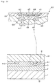
adhesive layer 5 is formed on the transferred layer (cleaved member) 4 to bond the transferredlayer 4 to themember 6, onto which the transferred layer is to be transferred, with theadhesive layer 5 provided therebetween. Preferable examples of the adhesives for constituting theadhesive layer 5 include curable adhesives, for example, reactive curing adhesives, thermosetting adhesives, photosetting adhesives, such as UV curable adhesives, and anaerobic curing adhesives. The types of the adhesive include epoxys, acrylates, and silicones. Theadhesive layer 5 may be formed by, for example, a coating process.When the above curing adhesive is used, the curing adhesive is coated on the transferredlayer 4, and themember 6 is bonded thereon, and then the curable adhesive is cured by a curing method depending on the property of the curable adhesive to bond the transferredlayer 4 to the member 6.When a photosetting adhesive is used, it is preferable that atranslucent member 6 be provided on the uncuredadhesive layer 5 and then that themember 6 be irradiated with light to cure the adhesive. Atranslucent substrate 1 is preferably used since the adhesive can be cured by light which are incident on thesubstrate 1 and themember 6 to secure curing.Theadhesive layer 5 may be formed on themember 6 and then the transferredlayer 4 may be bonded thereto, instead of the order shown in the drawing. The above-mentioned intermediate layer may be provided between the transferredlayer 4 and theadhesive layer 5. When themember 6 itself has an adhesive function, the formation of theadhesive layer 5 may be omitted.A nonlimiting example of themember 6 is a substrate (plate), and particularly a transparent substrate. Such a substrate may be flat or curved.Themember 6 onto which the transferred layer is transferred may be inferior to thesubstrate 1 in characteristics, such as heat resistance and corrosion resistance. Since the transferredlayer 4 is formed on thesubstrate 1 and is then transferred onto themember 6, the properties required for themember 6, including heat resistance, do not depend on the temperature when the transferredlayer 4 is transferred.When the maximum temperature when the transferredlayer 4 is formed is Tmax, materials having a glass transition point (Tg) or a softening point which is lower than Tmax can be used for themember 6. For example, themember 6 may be composed of a material having a glass transition point (Tg) or softening point of preferably 800°C or less, more preferably 500°C or less, and more preferably 320°C or less.In mechanical characteristics, themember 6 preferably has a certain level of rigidity (strength), but may have flexibility or elasticity. Materials for themember 6 include various synthetic resins and glasses, and various synthetic resins and inexpensive conventional glass materials having a low melting point are preferable.The synthetic resins may be thermoplastic resins or thermosetting resins. Examples of the synthetic resins include polyolefins, such as polyethylene, polypropylene, ethylene-propylene copolymers, and ethylene-vinyl acetate copolymers (EVA); cyclic polyolefins; modified polyolefins; polyvinyl chloride; polyvinylidene chloride; polystyrene; polyamides; polyimides; polyamide-imide resins; polycarbonates; poly-(4-methylpentene-1); ionomers; acrylic resins: polymethyl methacrylate (PMMA); acrylonitrilebutadiene-styrene copolymers (ABS resins); acrylonitrilestyrene copolymers (AS resins); butadiene-styrene copolymers; polyoxymethylene; polyvinyl alcohol (PVA); ethylene-vinyl alcohol copolymers (EVOH); polyesters, such as polyethylene terephthalate (PET), polybutylene terephthalate (PBT) and polycyclohexane terephthalate (PCT); polyethers; polyether ketones (PEK); polyether ether ketones (PEEK); polyether imides; polyacetals (POM); polyphenylene oxide; modified polyphenylene oxide; polysulfone; polyphenylene sulfide (PPS); polyether sulfone (PES); polyarylate; aromatic polyesters (liquid crystal polymers); polytetrafluoroethylene; polyvinylidene fluoride; miscellaneous fluorinated resins; thermoplastic elastomers, including styrenic elastomers, polyolefin, polyvinyl chloride, polyurethanes, polyesters, polyamides, polybutadiene, transpolyisoprene, fluorinated rubbers, and chlorinated polyethylene; epoxy resins; phenol resins; urea resins; melamine resins; unsaturated polyesters; silicone resins; polyurethanes; and copolymers, blends and polymer alloys thereof. These resins may be used alone or in combination, for example, as a composite including two or more layers.Examples of glass materials include silicate glass (quartz glass), alkaline silicate glass, soda-lime glass, potassium-lime glass, lead (alkaline) glass, barium glass, and borosilicate glass. These glasses other than silicate glass have low melting points compared to the silicate glass, are readily formable and workable, are inexpensive, and are preferable.When themember 6 is composed of a synthetic resin, alarge member 6 is integrally formed and a complicated shape such as curved or irregular face can be readily formed. Additional advantages are low costs of materials and production. Thus, a large inexpensive device, for example, a liquid crystal display, can be readily produced.Themember 6 may be an independent device such as a liquid crystal cell or may be a part of a device, for example, a color filter, an electrode layer, a dielectric layer, an insulating layer, or a semiconductor device.Themember 6 may be metal, ceramic, stone, wood or paper. Alternatively, themember 6 may be an appropriate face of an article (a board of a clock, a surface of an air conditioner, or a surface of a printed circuit board), or a surface of a structural unit, such as a wall, a column, a ceiling, or a window glass. - 〈5〉 As shown in Fig. 5, the back side of the substrate 1
(light incident side 12) is irradiated with the illuminating
light 7. The illuminating light 7 passes through thesubstrate 1, and is incident on thecleaving layer 2 via theinterface 2a. As shown in Fig. 6 or 7, intralayer cleavage and/or interfacial cleavage thereby occur in thecleaving layer 2. When thesubstrate 1 is peeled from themember 6, the transferredlayer 4 is detached from thesubstrate 1 and is transferred onto themember 6 due to decreased or lost bonding force. Fig. 6 shows intralayer cleavage in thecleaving layer 2, whereas Fig. 7 shows interfacial cleavage at theinterface 2a of thecleaving layer 2. The occurrence of the intralayer cleavage and/or interfacial cleavage is presumably due to ablation in the material constituting thecleaving layer 2, gas evolution included in thecleaving layer 2, and phase change by the irradiation such as melting or vaporization.Herein "ablation" means that a solid material which absorbs the illuminating light is photochemically or thermally excited and atomic or molecular bonds on the surface and in the interior are broken, and is observed as a phenomenon causing a phase change in which all or a part of the material in thecleaving layer 2 is melted or vaporized. Alternatively, the phase change may cause formation of fine pores which result in decreased bonding force.Whether thecleaving layer 2 forms intralayer cleavage, interfacial cleavage, or simultaneous intralayer and interfacial cleavages depends on the composition of thecleaving layer 2 and various factors. Some of the factors are the type, wavelength, intensity, and penetration depth of the illuminating light 7.Any illuminating light 7 may be used as long as it causes intralayer cleavage and/or interfacial cleavage in thecleaving layer 2. Examples of the illuminating light 7 include x-rays, ultraviolet rays, visible rays, infrared rays (heat rays), laser beams, millimeter waves, microwaves, electron beams, and radiations (α-rays, β-rays, and γ-rays). Among these, laser beams are preferable since they readily cause cleavage (ablation) in the cleaving layer 2.Examples of laser units for forming laser beams include gas lasers and solid lasers (semiconductor lasers). Excimer laser, Nd-YAG laser, Ar laser, CO2 laser, and He-Ne laser are preferable. Among these, the excimer laser is more preferable.Since the excimer laser outputs high energy in a short wave region, it can cause ablation in thecleaving layer 2 within a very short period. Thus, thecleaving layer 2 can be cleaved without substantial temperature rise and thus without deterioration and damage in theintermediate layer 3, the transferredlayer 4, and thesubstrate 1 in the proximity or vicinity thereof.When the ablation in thecleaving layer 2 depends on the wavelength of the illuminatinglight 7, the wavelength of the illuminatinglight 7 is preferably in a range of approximately 100 to 350 nm.When a phase change such as gas evolution, vaporization or sublimation imparts cleaving characteristics to thecleaving layer 2, the wavelength of the illuminating laser beam is preferably in a range of approximately 350 to 1,200 nm.The energy density of the illuminating laser beam and particularly the excimer laser beam is in a range of preferably 10 to 5,000 mJ/cm2, and more preferably 100 to 500 mJ/cm2. The irradiation time is in a range of preferably 1 to 1,000 nsec, and more preferably 10 to 100 nsec. When the energy density is low or the irradiation time is short, sufficient ablation does not occur. When the energy density is high or the irradiation time is long, the light passing through thecleaving layer 2 and theintermediate layer 3 may adversely affect the transferred layer 4.The illuminating light 7 such as a laser light beam is preferably radiated so that the intensity is uniform.The illuminating light 7 may be incident on thecleaving layer 2 not only perpendicularly but also slantingly with a given angle to the cleaving layer 2.When the area of thecleaving layer 2 is larger than the area of one spot of the illuminating light, the entire region of thecleaving layer 2 can be irradiated with a plurality of spots of the illuminating light. The same position may be irradiated with two or more spots.The same region or different regions may be irradiated with two or more spots of different types and different wavelengths (wavelength regions) of illuminating light (laser beams). - 〈6〉 As shown in Fig. 8, the
cleaving layer 2 adhered to theintermediate layer 3 is removed by a cleaning, etching, ashing, or polishing method, or by a combination thereof. -
- In the intralayer cleavage of the
cleaving layer 2 as shown in Fig. 6, thecleaving layer 2 adhered to thesubstrate 1 is also removed. - When the
substrate 1 is composed of an expensive or rare material, such as quartz glass, thesubstrate 1 is preferably reused or recycled. In other words, the present invention is applicable to thesubstrate 1 for which reuse is preferable, and thus is very useful. - The transfer of the transferred
layer 4 onto themember 6 is completed by the above steps. In the subsequent steps, theintermediate layer 3 adjoining the transferredlayer 4 may be removed or any other layer may be formed thereon. - In the present invention, the transferred
layer 4 as the cleaved member is not directly cleaved but thecleaving layer 2 bonded to the transferredlayer 4 is cleaved. Thus, thecleaving layer 2 can be readily, securely, and uniformly cleaved or transferred regardless of the properties of the cleaved member (transferred layer 4) and the conditions. Since the cleaved member (transferred layer 4) is not damaged during the cleaving operation, the transferredlayer 4 can maintain high reliability. - In the embodiment shown in the drawings, the illuminating
light 7 is incident on thesubstrate 1. When the illuminatinglight 7 does not affect the transferredlayer 4, the side away from thesubstrate 1 may be irradiated with the illuminatinglight 7, without limiting the direction of the illuminatinglight 7. - The
cleaving layer 2 may be partly irradiated with the illuminating light along the plane thereof, that is, with light having a given pattern so that the transferredlayer 4 having the pattern is transferred (first method). In this case, thelight incident side 12 of thesubstrate 1 is subjected to masking corresponding to the pattern before irradiation of the illuminating light 7 in the step 〈5〉, or the positions irradiated with the illuminating light 7 are precisely controlled. - Alternatively, a
cleaving layer 2 having a predetermined pattern can be formed (second method) instead of the formation of thecleaving layer 2 on the entire cleavinglayer forming face 11. In this case, acleaving layer 2 having the predetermined pattern is previously formed by masking or the like, or thecleaving layer 2 formed on the entire cleavinglayer forming face 11 is patterned or trimmed by etching or the like. - According to the first and second methods, the transfer of the transferred
layer 4 can be simultaneously achieved together with the patterning and trimming. - Transfer operations may be repeated two or more times by the above procedure. When the transfer operations are repeated an even number of times, the relationship of the front-back of the transferred layer formed on the last member onto which the transferred layer is transferred is the same as that of the transferred layer originally formed on the
substrate 1. - Transferred layers 4 (thin film transistors) having a small unit formed on a
small substrate 1 having, for example, an effective area of 45 mm × 40 mm can be sequentially transferred onto the adjacent positions of a large transparent substrate having, for example, an effective area of 900 mm × 1,600 mm a plurality of times (for example, approximately 800 times) to form the transferredlayer 4 onto the entire effective area of the large transparent substrate). A liquid crystal display having the same size as that of the large transparent substrate can be thereby produced. - A plurality of transferred
layers 4 formed on thesubstrates 1 may be sequentially transferred (overlapped) onto themember 6 to form a composite of the transferred layers 4. In this case, the transferredlayers 4 to be overlapped may be the same or different. - The method for transferring the thin film configuration used in the present invention has been described above.
- A first embodiment of a method for making a three-dimensional device (multilayered device) using the above-mentioned method for transferring a thin film configuration will now be described.
- Fig. 9 is a schematic cross-sectional view of a configuration of a three-dimensional device, and Figs. 10 to 15 are schematic cross-sectional views of the steps in the first embodiment of a method for making a three-dimensional device in accordance with the present invention. The common points with the above-described transfer process of the thin film configuration will not be described.
- As shown in Fig. 9, a three-
dimensional device 10 has a substrate (transferring-side substrate) 21 as a base, a first transferred layer (first thin film device layer) 41, and a second transferred layer (second thin film device layer) 42. The transferred layers 41 and 42 extend two-dimensionally (parallel to the substrate 21) to form a predetermined circuit. - In this case, the transferred
layer 41 is bonded on the upper side of thesubstrate 21 in Fig. 9 with anadhesive layer 5. - Also, the transferred
layer 42 is bonded on the upper side of the transferredlayer 41 in Fig. 9 with a conductiveadhesive layer 22. - The transferred
layer 41 has connecting electrodes (connecting terminals) 411 and 412 thereon in Fig. 9. The transferredlayer 42 has connecting electrodes (connecting terminals) 421 and 422 thereunder in Fig. 9. The connectingelectrode 411 of the transferredlayer 41 and the connectingelectrode 421 of the transferredlayer 42 are electrically connected to each other via the conductiveadhesive layer 22, whereas the connectingelectrode 412 of the transferredlayer 41 and the connectingelectrode 422 of the transferredlayer 42 are electrically connected to each other via the conductiveadhesive layer 22. - A preferable conductive
adhesive layer 22 is an anisotropic conductive film (ACF). Since bonding with the anisotropic conductive film enables conduction only in the thickness direction (the longitudinal direction in Fig. 9), short-circuiting in the transverse direction in Fig. 9 is prevented. That is, short-circuiting between the connectingelectrodes electrodes electrodes electrodes - In the bonding with the anisotropic conductive film, the transferred
layer 41 and the transferredlayer 42 are bonded to each other while the connectingelectrodes electrodes - The substrate (transferring-side substrate) 21 of the three-
dimensional device 10 corresponds to themember 6 onto which the transferred layer is transferred in Figs. 4 to 8. - Examples of the transferred layers 41 and 42 of the three-
dimensional device 10 include the above-described various types as the transferred layers 4. - That is, the transferred layers 41 and 42 may be dynamic RAMs (DRAMs), static RAMs (SRAMs), memories such as E2PROMs and ROMs, logics (logic circuits) such as CPU, and sensors such as an optical sensor or a magnetic sensor. Of course, the transferred layers 41 and 42 are not limited to the above examples.
- The transferred layers 41 and 42 may be the same or different.
- When the transferred layers 41 and 42 are the same, the transferred
layer 41 and the transferredlayer 42 may be, for example, memories (memory cell arrays). A large-capacity memory (integrated memory) is thereby achieved. - Alternatively, the transferred
layer 41 and the transferredlayer 42 may be, for example, logics (logic circuits). A large-capacity logic (integrated logic) is thereby achieved. - In an example in which the transferred
layer 41 and the transferredlayer 42 are different, for example, one of the transferredlayer 41 and the transferredlayer 42 is a memory and the other is a logic. That is, the three-dimensional device 10 is a system IC (for example, a system LSI) including (or integrating) a memory and a logic. - In such a case, the transferred
layer 41 and the transferredlayer 42 can be formed using different design rules (minimum line widths) according to the present invention. The transferredlayer 41 and the transferredlayer 42 can also be formed using different design parameters. Alternatively, the transferredlayer 41 and the transferredlayer 42 can be formed by different production processes. In conventional methods, it is impossible or difficult to change such conditions between the layers to be deposited. - The minimum line width of the memory in the system IC is, for example, approximately 0.35 µm (µm rule), and the minimum line width of the logic is, for example, approximately 0.5 µm (µm rule) (the minimum line width of the memory is smaller than the minimum line width of the logic). In contrast, the minimum width of the memory may be larger than the minimum width of the logic.
- The three-
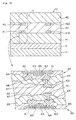
dimensional device 10 is produced by the above-mentioned transfer process of a thin film configuration, for example, as follows. - 〈A1〉 As shown in Fig. 10, a
cleaving layer 2 is formed on one face of a substrate (original substrate) 1. As shown in Fig. 11, acleaving layer 2 is formed on one face of a substrate (original substrate) 1. - 〈A2〉 As shown in Figs. 10 and 11, an intermediate layer
(underlying layer) 3 is formed on the
cleaving layer 2 of eachsubstrate 1. - 〈A3〉 As shown in Fig. 10, a first transferred layer (first
thin film device layer) 41 is formed on the
intermediate layer 3. As shown in Fig. 11, a second transferred layer (second thin film device layer) 42 is formed on theintermediate layer 3. An enlarged cross-sectional view of the portion K (surrounded by a chain line in Fig. 10) of the transferredlayer 41 is shown in Fig. 10.As shown in Fig. 10, the transferredlayer 41 has, for example, a thin film transistor (TFT) 60 formed on the intermediate layer 3 (for example a SiO2 film).Thethin film transistor 60 includes a source layer (n+ or p+ layer) 61 and a drain layer (n+ or p+ layer) 62 which are formed by doping an n- or p-type impurity into a polysilicon layer, achannel layer 63, agate insulating layer 64, agate electrode 65, an insulatinginterlayer 66,electrodes electrode 411 is formed under theprotective film 69 of thethin film transistor 60 in Fig. 10. The connectingelectrode 411 is electrically connected to theelectrode 68 via a contact hole formed in the protective film 69.An enlarged cross-sectional view of the portion K (surrounded by a chain line in Fig. 11) of the transferredlayer 42 is shown in Fig. 11. As shown in Fig. 11, the transferredlayer 42 has, for example, a thin film transistor (TFT) 60 formed on the intermediate layer 3 (for example a SiO2 film).Thethin film transistor 60 includes a source layer (n+ or p+ layer) 61 and a drain layer (n+ or p+ layer) 62 which are formed by doping an n- or p-type impurity into a polysilicon layer, achannel layer 63, agate insulating layer 64, agate electrode 65, an insulatinginterlayer 66,electrodes electrode 421 is formed on theprotective film 69 of thethin film transistor 60 in Fig. 11. The connectingelectrode 421 is electrically connected to theelectrode 67 via a contact hole formed in the protective film 69.The configurations of the transferredlayer 41 in the vicinity of theelectrode 412 and the transferredlayer 42 in the vicinity of theelectrode 422 are substantially the same as the above-described configuration, and the description is omitted.In the present invention, many transferredlayers 41 may be simultaneously formed on one substrate, for example, a glass substrate, not shown in the drawing, and then may be cut off. Similarly, many transferredlayers 42 may be simultaneously formed on one substrate, for example, a glass substrate, not shown in the drawing, and then may be cut off.Each substrate provided with the transferredlayer layer layer layers layer 41 and the transferredlayer 42 may be simultaneously formed, particularly on the same substrate (original substrate) 1. The production steps can be thereby reduced. - 〈A4〉 As shown in Fig. 12, the transferred
layer 41 formed on thesubstrate 41 is bonded to a substrate (transferred-side substrate) 21 with anadhesive layer 5. - 〈A5〉 As shown in Fig. 12, the back face (light incident face
12) of the
substrate 1 is irradiated with illuminatinglight 7. The illuminating light 7 passes through thesubstrate 1, and is incident on thecleaving layer 2 to cause intralayer cleavage and/or interfacial cleavage in thecleaving layer 2 and thus to decrease or eliminate bonding force. Thesubstrate 1 is detached from thesubstrate 21. As shown in Fig. 13, the transferredlayer 41 is detached from thesubstrate 1 and is transferred onto thesubstrate 21. - 〈A6〉 As shown in Fig. 13, the
intermediate layer 3 and thecleaving layer 2 on the transferredlayer 41 is removed by a cleaning, etching, ashing, or polishing method, or by a combination thereof. Theintermediate layer 3 may remain so as to expose the connectingelectrodes cleaving layer 2, thecleaving layer 2 remaining on thesubstrate 1 is also removed.When thesubstrate 1 is composed of an expensive or rare material, such as quartz glass, thesubstrate 1 is preferably reused or recycled. In other words, the present invention is applicable to thesubstrate 1 for which reuse is preferable, and thus is very useful.The transfer of the transferredlayer 41 onto thesubstrate 21 is completed by the above steps. In the subsequent step, any other layer may be formed thereon. - 〈A7〉 As shown in Fig. 14, the corresponding connecting
electrodes are positioned so that these electrodes are
opposite each other, that is, the connecting
electrode 411 is opposite the connectingelectrode 421 and the connectingelectrode 412 is opposite the connectingelectrode 422, while the transferredlayer 42 formed on thesubstrate 1 is bonded to the transferredlayer 41 transferred onto thesubstrate 21 with a conductiveadhesive layer 22. Although the conductiveadhesive layer 22 is preferably an anisotropic conductive film, it is not limited thereto in the present invention.When bonding is performed using the anisotropic conductive film, the anisotropic conductive film is supplied between the transferredlayer 41 and the transferredlayer 42 and cured while pressing in the longitudinal direction in Fig. 14. Thus, the transferredlayer 41 and the transferredlayer 42 are bonded to each other with the conductiveadhesive layer 22, and conductive particles (not shown in the drawing) in the conductiveadhesive layer 22 are connected (are put into contact with each other) in the longitudinal direction in Fig. 14 so that the connectingelectrodes electrodes - 〈A8〉 As shown in Fig. 14, the back face (the light incident
face 12) of the
substrate 1 is irradiated with the illuminatinglight 7. As described above, the illuminating light 7 passes through thesubstrate 1, and is incident on thecleaving layer 2 to cause intralayer cleavage and/or interfacial cleavage in thecleaving layer 2 and thus to decrease or eliminate bonding force. Thesubstrate 1 is detached from thesubstrate 21. As shown in Fig. 15, the transferredlayer 42 is detached from thesubstrate 1 and is transferred onto the transferred layer 41.An enlarged cross-sectional view of the portion K (surrounded by a chain line in Fig. 15) including the transferred layers 41 and 42 and the conductiveadhesive layer 22 is shown in Fig. 15. - 〈A9〉 As shown in Fig. 15, the
intermediate layer 3 and thecleaving layer 2 on the transferredlayer 42 is removed by a cleaning, etching, ashing, or polishing method, or by a combination thereof. Theintermediate layer 3 may remain, if necessary. -
- In the case of the intralayer cleavage in the
cleaving layer 2, thecleaving layer 2 remaining on thesubstrate 1 is also removed. - When the
substrate 1 is composed of an expensive or rare material, such as quartz glass, thesubstrate 1 is preferably reused or recycled. In other words, the present invention is applicable to thesubstrate 1 for which reuse is preferable, and thus is very useful. - The transfer of the transferred
layer 42 onto the transferredlayer 41, that is, deposition of the transferredlayer 42 onto the transferredlayer 41 is completed by the above steps. In the subsequent step, any other layer may be formed thereon. - As described above, a three-dimensional device, for example, a three-
dimensional IC 10 can be readily produced by transfer according to the present invention. - Since individual thin film device layers can be independently produced, wide ranges of production conditions can be selected without considering adverse effects on the underlying layers (underlying thin film device layers), unlike conventional processes.
- Since a plurality of thin film device layers is deposited in the present invention, integration density is increased. Thus, ICs can be formed in a relatively small area even by a relatively moderated design rule.
- For example, when the three-
dimensional device 10 has memories (when both the transferred layers 41 and 42 are memories), the memories have a large capacity. When the three-dimensional device 10 has logics (when both the transferred layers 41 and 42 are logics), the logics have a large scale. Since individual thin film device layers can be formed on different substrates in the present invention, each thin film device layer can be formed by appropriate device parameters, for example, a gate line width, a thickness of the gate insulating film, a design rule, and production conditions such as temperature. Since each thin film device layer can be formed by optimized device parameters, the resulting three-dimensional device 10 has high reliability and high performance. - For example, when the three-
dimensional device 10 is a system IC (for example, a system LSI) including (or integrating) a memory and a logic, the memory and the logic can be formed by desirable processes in the production of the system IC, resulting in readily production, high productivity, and advantageous mass production. - Since a connecting electrode (connecting terminal) is formed at one end of each thin film device layer, adjacent thin film device layers can be readily, securely, and electrically connected. Thus, the three-
dimensional device 10 has a three-dimensional configuration (has a three-dimensional circuit). - Since only nondefective units are selected in deposition of each thin film device layer, the product yield is improved compared to production of three-dimensional devices by deposition of each layer on the same substrate (direct formation of each layer).
- Transfer can be performed onto various substrates 21 (transferred-side substrates) without limitation. That is, a thin film device layer can be formed by transfer onto a substrate composed of a material which is not capable of or suitable for direct formation of the thin film device layer, which can be readily shaped, or which is inexpensive. In other words, the
substrate 21 is appropriately selected. Since ICs can be formed on a flexible substrate, and IC cards and the like can be readily produced. - Since a relatively inexpensive glass substrate having a large area can be used as the substrate (original substrate) 1, cost is reduced.
- In the above-described embodiment, the transfer of the transferred layers (thin film device layers) 41 and 42 is performed once. In the present invention, the transfer of the transferred
layer 41 may be performed two or more times and the transfer of the transferredlayer 42 may be performed two or more times, as long as the transferredlayer 41 and the transferredlayer 42 can be deposited. - For example, when the transferred layer is transferred twice, the transferred layer on the
substrate 1 is transferred onto a third substrate (not shown in the drawing), not onto thesubstrate 1 and thesubstrate 21, and then the transferred layer on the third substrate is transferred onto thesubstrate 21. The above-describedcleaving layer 2 is previously formed on the third substrate. - When the transferred layer is transferred an even number of times, the relationship of the front-back of the transferred layer formed on the substrate (transferred-side substrate) 21 being the last member onto which the transferred layer is transferred is the same as that of the transferred layer originally formed on the substrate (original substrate) 1.
- In the present invention, a transferred
layer 41 may be directly formed onto the substrate (transferring-side substrate) 21 and a transferredlayer 42 may be transferred onto the transferredlayer 41 by the above-described transfer process to produce a three-dimensional device 10. - Three or more transferred layers (thin film device layers) may be deposited in the present invention. An increase in the deposited transferred layers causes an increase in integration density.
- For example, when the three-
dimensional device 10 has three transferred layers (thin film device layers) and when the adjacent transferred layers are electrically connected to each other, connecting electrodes (connecting terminals) are formed at both ends of a third transferred layer (third thin film device layer) 43 disposed between a first transferred layer (first thin film device layer) 41 and a second transferred layer (second thin film device layer) 42. That is, connectingelectrodes electrodes - The connecting
electrode 411 of the transferredlayer 41 and the connectingelectrode 431 of the transferredlayer 43 are electrically connected via a conductiveadhesive layer 22, and the connectingelectrode 412 of the transferredlayer 41 and the connectingelectrode 432 of the transferredlayer 43 are electrically connected via the conductiveadhesive layer 22. Similarly, the connectingelectrode 433 of the transferredlayer 43 and the connectingelectrode 421 of the transferredlayer 42 are electrically connected via a conductiveadhesive layer 23, and the connectingelectrode 434 of the transferredlayer 43 and the connectingelectrode 422 of the transferredlayer 42 are electrically connected via the conductiveadhesive layer 23. - A preferable conductive
adhesive layer 23 is an anisotropic conductive film for the same reason as that for the conductiveadhesive layer 22. - When the transferred layers (thin film device layers) are deposited three or more times, these layers may be completely the same or different, or may be partially the same.
- A second embodiment of a method for making a three-dimensional device will now be described.
- Fig. 17 is a schematic cross-sectional view of a configuration of a three-dimensional device. The common points with the above-described first embodiment are not described, and main differences will be described.
- A three-
dimensional device 10 shown in Fig. 17 is also produced by a transfer process of a thin film configuration as in the first embodiment. - In this three-
dimensional device 10, in the above step 〈A7〉, the connectingelectrode 411 of the first transferred layer (first thin film device layer) 41 is put into contact with the connectingelectrode 421 of the second transferred layer (second thin film device layer) 42 to electrically connect these layers, the connectingelectrode 412 of the transferredlayer 41 is put into contact with the connectingelectrode 422 of the second transferredlayer 42 to electrically connect these layers, and the transferredlayer 41 and the transferredlayer 42 are bonded to each other with anadhesive layer 24. - The second embodiment also has the same advantages as that of the first embodiment.
- In the present invention, the method for bonding the transferred
layer 41 to the transferredlayer 42 and the method for electrically connecting the corresponding connecting electrodes are not limited to those described in the first embodiment and the second embodiment. - For example, the connecting
electrodes electrodes layer 41 and the transferredlayer 42 are bonded. - Alternatively, a solder (conductive brazing agent) may be disposed between the connecting
electrode 411 and the connectingelectrode 421 and between the connectingelectrode 412 and the connectingelectrode 422, may be heated to be melted, and may then be solidified. As a result, the corresponding connecting electrodes are electrically connected via the solder and the transferredlayer 41 and the transferredlayer 42 are bonded with the solder. - A third embodiment of a method for making a three-dimensional device will now be described.
- Fig. 18 is a schematic cross-sectional view of a configuration of a three-dimensional device. The common points with the above-described first embodiment are not described, and main differences will be described.
- A three-
dimensional device 10 shown in Fig. 18 is also produced by a transfer process of a thin film configuration as in the first embodiment. - A light emitting section (luminescent device) 413 and a light receiving section (light receiving device) 414 are formed on one face of a first transferred layer (first thin film device layer) 41 (the upper side in Fig. 18) of the three-
dimensional device 10. - Also, a light emitting section (luminescent device) 423 and a light receiving section (light receiving device) 424 are formed on one face of a second transferred layer (second thin film device layer) 42 (the lower side in Fig. 18).
- In this three-
dimensional device 10, in the above step 〈A7〉, positioning is performed so that the light emitting sections are opposite the corresponding light receiving section, that is, thelight emitting section 413 is opposite thelight receiving section 424 and the light emitting section 423 is opposite thelight receiving section 414, while the transferredlayer 41 and the transferredlayer 42 are bonded to each other with a substantially transparent adhesive layer 25 (having transmissivity to light from thelight emitting sections 413 and 423). - For example, organic EL devices can be used as the
light emitting sections 413 and 423 in the three-dimensional device 10. - Fig. 19 is a cross-sectional view of a configuration of an organic electroluminescent (EL) device.
- As shown in the drawing, an
organic EL device 30 has a barrier (bank) 34, atransparent electrode 31 and a light emitting layer (organic EL) 32 formed in thebarrier 34, and ametallic electrode 33. - In this case, the
light emitting layer 32 is formed on thetransparent electrode 31, and themetallic electrode 33 is formed on thebarrier 34 and thelight emitting layer 32. - The
transparent electrode 31 is composed of, for example, ITO. - The
light emitting layer 32 is composed of a thin film (solid thin film) obtained by heating an organic EL device composition in which a precursor of a conjugated organic polymer for forming thelight emitting layer 32 and a fluorescent pigment for modifying the luminescent characteristics of thelight emitting layer 32 are dissolved or dispersed into a given solvent (polar solvent) so that the precursor in the organic EL device composition is polymerized. - The
metallic electrode 33 is composed of, for example, Al-Li. - The
barrier 34 is composed of, for example, a resin black resist. - Each of the transferred layers 41 and 42 has a driving section (driving circuit) (not shown in the drawing) for driving the
organic EL device 30. - When a given voltage is applied between the
transparent electrode 31 and themetallic electrode 33 from the driving circuit in theorganic EL device 30, electrons and holes are injected into thelight emitting layer 32, and moved in thelight emitting layer 32 by means of an electric field formed by the applied voltage, and recombined. The energy evolved during the recombination forms excitons, and the excitons return to the ground state while evolving energy (fluorescent or phosphorescent light). Such a phenomenon is called electroluminescence (EL). - For example, PIN photodiodes may be used as the
light receiving sections dimensional device 10. - Fig. 20 is a cross-sectional view of a configuration of a PIN photodiode.
- As shown in the drawing, a
PIN photodiode 50 includes a light-receivingsection window electrode 51, a p-type a-SiC layer (p-type semiconductor layer) 52, an i-type a-SiC layer (i-type semiconductor layer) 53, an n-type a-SiC layer (n-type semiconductor layer) 54, and an Al-Si-Cu layer 55 functioning as a light-receiving section upper electrode and a lead line (electrical line). - The light-receiving
section window electrode 51, the p-type a-SiC layer 52, the i-type a-SiC layer 53, the n-type a-SiC layer 54, and the Al-Si-Cu layer 55 are deposited in that order from the bottom side in Fig. 20. The light-receivingsection window electrode 51 is composed of, for example, ITO. - As described above, the
organic EL device 30 is driven by a driving circuit (not shown in the drawing) electrically connected to theorganic EL device 30 to emit light. That is, theorganic EL device 30 submits optical signals (light). - The light from the
organic EL device 30 passes through theadhesive layer 25 and is incident on the light-receivingsection window electrode 51. That is, thePIN photodiode 50 receives the light. - The
PIN photodiode 50 outputs a current, i.e., an electrical signal in response to the intensity of the received light (the optical signal is output as an electrical signal). - A circuit (not shown in the drawing) electrically connected to the
PIN photodiode 50 operates based on the signal from thePIN photodiode 50. - As shown in Fig. 18, the light from the
light emitting section 413 passes through theadhesive layer 25 and is incident on thelight receiving section 424, and the light from the light emitting section 423 passes through theadhesive layer 25 and is incident on thelight receiving section 414. That is, thelight emitting sections 413 and 423 and thelight receiving sections layer 41 and the transferredlayer 42. - The third embodiment also has the same advantages as that of the first embodiment.
- In the configuration in the third embodiment, signal transmittance between layers is performed by optical signals, not by electrical signals. Thus, production is facilitated and integration density can be further increased.
- In the present invention, the
light emitting sections 413 and 423 may be composed of inorganic EL devices, light emitting diodes (LEDs), or semiconductor lasers (laser diodes), in addition to the organic EL devices. - In the present invention, the
light receiving sections - The bonding method of the transferred layer (thin film device layer) 41 and the transferred layer (thin film device layer) 42 is not limited to the above-described method. That is, the transferred
layer 41 and the transferredlayer 42 are bonded to each other so that optical communication is achieved between the transferredlayer 41 and the transferredlayer 42. - For example, the transferred
layer 41 and the transferredlayer 42 can be partly bonded to each other. When bonding is performed at the sections other than thelight emitting sections 413 and 423 and thelight receiving sections layer 41 and the transferredlayer 42 may be bonded to each other with an opaque adhesive layer. - The transferred
layer 41 and the transferredlayer 42 may be bonded to each other with a spacer (for example, a column) provided between the transferredlayer 41 and the transferredlayer 42. In such a case, gaps are formed between thelight emitting section 413 and thelight receiving section 414 of the transferredlayer 41 and between the light emitting section 423 and thelight receiving section 424 of the transferredlayer 42. - The
light emitting section 413 of the transferredlayer 41 may be put into contact with thelight receiving section 414, and thelight emitting section 424 of the transferredlayer 42 may be put into contact with the light receiving section 423. - When the number of the transferred layers (thin film device layers) in the three-dimensional device is three or more, this embodiment may include a configuration enabling optical communication between layers which are not adjacent to each other.
- In the present invention, the light emitting section may consist of a plurality of luminescent devices having different luminescent characteristics (for example, peak wavelengths of the luminescent light) and the light receiving section may consist of a plurality of light receiving devices for receiving the light from the corresponding luminescent devices.
- In such a case, a plurality of information signals can be simultaneously transmitted. That is, information transmission by multichannel optical communication is achieved.
- In the present invention, a plurality of light emitting sections having different luminescent characteristics (for example, peak wavelengths of the luminescent light) may be provided and a plurality of light receiving sections may be provided for receiving the light from the corresponding light emitting sections.
- The present invention also includes a configuration, which can achieve optical communication in at least a given transferred layer (thin film device layer), as in that between the transferred layers (thin film device layers).
- The method for making the three-dimensional device of the present invention has been described above with reference to the embodiments shown in the drawings, but the present invention is not limited thereto.
- For example, when the number of the transferred layers (thin film device layers) is three or more in the present invention, given transferred layers may be electrically connected to each other as in the first and second embodiments, whereas the other transferred layers may be optically connected to each other as in the third embodiment so as to enable optical communication.
- In the present invention, partial regions of given transferred layers may be electrically connected to each other and the other regions may be optically connected to each other.
- In the present invention, a three-dimensional device may be produced by transferring at least one layer among a plurality of transferred layers (thin film device layers) in the three-dimensional device by the above-mentioned transfer process (transfer technology) of the thin film configuration.
- The transfer process in the present invention is not limited to the above-described method.
- In accordance with the method for making a three-dimensional device of the present invention, as described above, since thin film device layers are deposited by a transfer process, the three-dimensional device, for example, a three-dimensional IC is readily produced.
- In particular, wide ranges of production conditions can be selected without considering adverse effects on the underlying layers (underlying thin film device layers), unlike in conventional processes, because individual thin film device layers can be independently produced.
- Since a plurality of thin film device layers is deposited in the production of the device in the present invention, integration density is increased.
- Since individual thin film device layers are formed on different substrates in the present invention, each thin film device layer can be formed by optimized device parameters, and the resulting device has high reliability and high performance.
- Since only nondefective units are selected in deposition of each thin film device layer, the product yield is improved compared to production of three-dimensional devices by deposition of each layer on the same substrate (direct formation of each layer).
Claims (22)
- A method for making a three-dimensional device comprising depositing in the thickness direction a plurality of thin film device layers disposed in a predetermined region in the two-dimensional direction, wherein at least one of the thin film device layers is deposited by a transfer process.
- A method for making a three-dimensional device constituting a three-dimensional circuit comprising:depositing in the thickness direction a plurality of thin film device layers constituting a circuit in a predetermined region in the two-dimensional direction on a substrate,
wherein at least one of the thin film device layers is deposited by a transfer process. - A method for making a three-dimensional device according to either claim 1 or 2, wherein the transfer process comprises forming a thin film device layer on a first substrate with a cleaving layer provided therebetween, and irradiating the cleaving layer with illuminating light so as to form cleavage in the cleaving layer and/or at the interface thereof and to transfer the thin film device layer on the first substrate onto a second substrate side.
- A method for making a three-dimensional device according to claim 3, wherein the cleavage of the cleaving layer is generated by breakage or attenuation of atomic or molecular bonding force of substances constituting the cleaving layer.
- A method for making a three-dimensional device according to claim 3, wherein the cleavage of the cleaving layer is generated by gas evolved from the substance constituting the cleaving layer.
- A method for making a three-dimensional device according to claim 3, wherein the illuminating light is laser light.
- A method for making a three-dimensional device according to claim 6, wherein the wavelength of the laser light is 100 to 350 nm.
- A method for making a three-dimensional device according to claim 6, wherein the wavelength of the laser light is 350 to 1,200 nm.
- A method for making a three-dimensional device according to claim 3, wherein the cleaving layer comprises amorphous silicon, ceramic, metal or an organic polymer.
- A method for making a three-dimensional device according to claim 3, wherein the first substrate is a transparent substrate.
- A method for making a three-dimensional device according to claim 1, wherein each of the thin film device layers is provided with connecting electrodes, and the connecting electrodes electrically connect the two adjacent thin film device layers.
- A method for making a three-dimensional device according to claim 11, wherein the connecting electrodes are disposed on the two surfaces of the thin film device layer.
- A method for making a three-dimensional device according to claim 11, wherein the two adjacent thin film device layers are bonded to each other with an anisotropic conductive film therebetween.
- A method for making a three-dimensional device according to any one of claims 1 to 10, wherein in the two selected layers among the thin film device layers, one of the two selected layers is provided with a light emitting section and the other layer is provided with a light receiving section for receiving the light from the light emitting section, the light emitting section and the light receiving section enabling optical communication between the two layers.
- A method for making a three-dimensional device according to claim 1, wherein the thin film device layer deposited by the transfer is simultaneously produced with at least one of the other thin film device layers.
- A method for making a three-dimensional device according to claim 1, wherein at least one of the thin film device layers has a plurality of thin film transistors.
- A method for making a three-dimensional device according to claim 1, wherein the thin film device layers as memory are transferred a plurality of times to form a large-scale memory.
- A method for making a three-dimensional device according to claim 1, wherein the thin film device layers as logic are transferred a plurality of times to form a large-scale logic.
- A method for making a three-dimensional device according to claim 1, wherein the thin film device layers as memory and the thin film device layers as logic are transferred to form a system LSI.
- A method for making a three-dimensional device according to claim 19, wherein the logic and the memory are formed by different design rules.
- A method for making a three-dimensional device according to claim 19, wherein the logic and the memory are formed by different design parameters.
- A method for making a three-dimensional device according to claim 19, wherein the logic and the memory are formed by different production processes.
Applications Claiming Priority (3)
| Application Number | Priority Date | Filing Date | Title |
|---|---|---|---|
| JP04841098A JP4126747B2 (en) | 1998-02-27 | 1998-02-27 | Manufacturing method of three-dimensional device |
| JP4841098 | 1998-02-27 | ||
| PCT/JP1999/000819 WO1999044236A1 (en) | 1998-02-27 | 1999-02-23 | Method of manufacturing three-dimensional device |
Publications (2)
| Publication Number | Publication Date |
|---|---|
| EP0986104A1 true EP0986104A1 (en) | 2000-03-15 |
| EP0986104A4 EP0986104A4 (en) | 2003-07-30 |
Family
ID=12802546
Family Applications (1)
| Application Number | Title | Priority Date | Filing Date |
|---|---|---|---|
| EP99903937A Ceased EP0986104A4 (en) | 1998-02-27 | 1999-02-23 | Method of manufacturing three-dimensional device |
Country Status (7)
| Country | Link |
|---|---|
| US (1) | US6627518B1 (en) |
| EP (1) | EP0986104A4 (en) |
| JP (1) | JP4126747B2 (en) |
| KR (1) | KR100484959B1 (en) |
| CN (1) | CN1132245C (en) |
| TW (1) | TW426869B (en) |
| WO (1) | WO1999044236A1 (en) |
Cited By (16)
| Publication number | Priority date | Publication date | Assignee | Title |
|---|---|---|---|---|
| EP1017100A1 (en) * | 1998-03-02 | 2000-07-05 | Seiko Epson Corporation | Three-dimensional device |
| US7420208B2 (en) | 2001-06-20 | 2008-09-02 | Semiconductor Energy Laboratory Co., Ltd. | Light emitting device and method of manufacturing the same |
| US7554169B2 (en) | 2002-12-17 | 2009-06-30 | Semiconductor Energy Laboratory Co., Ltd. | Semiconductor device and method of manufacturing the same |
| US7691686B2 (en) | 2004-05-21 | 2010-04-06 | Semiconductor Energy Laboratory Co., Ltd. | Semiconductor device and manufacturing method thereof |
| US7728326B2 (en) | 2001-06-20 | 2010-06-01 | Semiconductor Energy Laboratory Co., Ltd. | Light emitting device and electronic apparatus |
| US7746333B2 (en) | 2003-02-12 | 2010-06-29 | Semiconductor Energy Laboratory Co., Ltd. | Semiconductor device |
| EP2381476A3 (en) * | 2004-11-11 | 2012-02-08 | Semiconductor Energy Laboratory Co., Ltd. | Semiconductor device |
| US8859347B2 (en) | 2009-07-15 | 2014-10-14 | Silanna Semiconductor U.S.A., Inc. | Semiconductor-on-insulator with back side body connection |
| US8912646B2 (en) | 2009-07-15 | 2014-12-16 | Silanna Semiconductor U.S.A., Inc. | Integrated circuit assembly and method of making |
| US9029201B2 (en) | 2009-07-15 | 2015-05-12 | Silanna Semiconductor U.S.A., Inc. | Semiconductor-on-insulator with back side heat dissipation |
| US9034732B2 (en) | 2009-07-15 | 2015-05-19 | Silanna Semiconductor U.S.A., Inc. | Semiconductor-on-insulator with back side support layer |
| US9390974B2 (en) | 2012-12-21 | 2016-07-12 | Qualcomm Incorporated | Back-to-back stacked integrated circuit assembly and method of making |
| US9419142B2 (en) | 2006-03-03 | 2016-08-16 | Semiconductor Energy Laboratory Co., Ltd. | Method for manufacturing semiconductor device |
| US9466719B2 (en) | 2009-07-15 | 2016-10-11 | Qualcomm Incorporated | Semiconductor-on-insulator with back side strain topology |
| US9496227B2 (en) | 2009-07-15 | 2016-11-15 | Qualcomm Incorporated | Semiconductor-on-insulator with back side support layer |
| US9515181B2 (en) | 2014-08-06 | 2016-12-06 | Qualcomm Incorporated | Semiconductor device with self-aligned back side features |
Families Citing this family (252)
| Publication number | Priority date | Publication date | Assignee | Title |
|---|---|---|---|---|
| US20050280155A1 (en) * | 2004-06-21 | 2005-12-22 | Sang-Yun Lee | Semiconductor bonding and layer transfer method |
| AU2001286432A1 (en) * | 2000-08-14 | 2002-02-25 | Matrix Semiconductor, Inc. | Dense arrays and charge storage devices, and methods for making same |
| TW521391B (en) * | 2001-01-26 | 2003-02-21 | Koninkl Philips Electronics Nv | Method of manufacturing a display device |
| US6897514B2 (en) * | 2001-03-28 | 2005-05-24 | Matrix Semiconductor, Inc. | Two mask floating gate EEPROM and method of making |
| JP4244120B2 (en) * | 2001-06-20 | 2009-03-25 | 株式会社半導体エネルギー研究所 | Light emitting device and manufacturing method thereof |
| US8415208B2 (en) * | 2001-07-16 | 2013-04-09 | Semiconductor Energy Laboratory Co., Ltd. | Semiconductor device and peeling off method and method of manufacturing semiconductor device |
| EP1455394B1 (en) | 2001-07-24 | 2018-04-11 | Samsung Electronics Co., Ltd. | Transfer method |
| US6814832B2 (en) | 2001-07-24 | 2004-11-09 | Seiko Epson Corporation | Method for transferring element, method for producing element, integrated circuit, circuit board, electro-optical device, IC card, and electronic appliance |
| JP5057619B2 (en) * | 2001-08-01 | 2012-10-24 | 株式会社半導体エネルギー研究所 | Method for manufacturing semiconductor device |
| TW554398B (en) * | 2001-08-10 | 2003-09-21 | Semiconductor Energy Lab | Method of peeling off and method of manufacturing semiconductor device |
| US7351300B2 (en) | 2001-08-22 | 2008-04-01 | Semiconductor Energy Laboratory Co., Ltd. | Peeling method and method of manufacturing semiconductor device |
| KR100478521B1 (en) * | 2001-10-29 | 2005-03-28 | 삼성에스디아이 주식회사 | Emitting composition mixture polymer and electroluminescence device using the same |
| TW594947B (en) | 2001-10-30 | 2004-06-21 | Semiconductor Energy Lab | Semiconductor device and method of manufacturing the same |
| TWI264121B (en) | 2001-11-30 | 2006-10-11 | Semiconductor Energy Lab | A display device, a method of manufacturing a semiconductor device, and a method of manufacturing a display device |
| US6953735B2 (en) | 2001-12-28 | 2005-10-11 | Semiconductor Energy Laboratory Co., Ltd. | Method for fabricating a semiconductor device by transferring a layer to a support with curvature |
| US7101729B2 (en) * | 2002-03-28 | 2006-09-05 | Seiko Epson Corporation | Method of manufacturing a semiconductor device having adjoining substrates |
| DE60325669D1 (en) * | 2002-05-17 | 2009-02-26 | Semiconductor Energy Lab | Method for transferring an object and method for producing a semiconductor device |
| JP4373063B2 (en) | 2002-09-02 | 2009-11-25 | 株式会社半導体エネルギー研究所 | Electronic circuit equipment |
| TW200421497A (en) * | 2002-11-20 | 2004-10-16 | Reveo Inc | Method and system for increasing yield of vertically integrated devices |
| TWI330269B (en) | 2002-12-27 | 2010-09-11 | Semiconductor Energy Lab | Separating method |
| JP4373085B2 (en) | 2002-12-27 | 2009-11-25 | 株式会社半導体エネルギー研究所 | Semiconductor device manufacturing method, peeling method, and transfer method |
| JP4574118B2 (en) * | 2003-02-12 | 2010-11-04 | 株式会社半導体エネルギー研究所 | Semiconductor device and manufacturing method thereof |
| JP2004349513A (en) * | 2003-05-22 | 2004-12-09 | Seiko Epson Corp | Thin film circuit device, its manufacturing method, electrooptic device, and electronic equipment |
| JP2004349540A (en) | 2003-05-23 | 2004-12-09 | Seiko Epson Corp | Method of manufacturing thin film device, electrooptical device, and electronic equipment |
| US7180064B2 (en) * | 2003-07-24 | 2007-02-20 | Delphi Technologies, Inc. | Infrared sensor package |
| JP2005081299A (en) * | 2003-09-10 | 2005-03-31 | Seiko Epson Corp | Method for forming film, method for forming circuit pattern, method for producing semiconductor device, electro-optical apparatus, and electronic apparatus |
| US6821826B1 (en) * | 2003-09-30 | 2004-11-23 | International Business Machines Corporation | Three dimensional CMOS integrated circuits having device layers built on different crystal oriented wafers |
| US6967149B2 (en) * | 2003-11-20 | 2005-11-22 | Hewlett-Packard Development Company, L.P. | Storage structure with cleaved layer |
| FR2863405B1 (en) * | 2003-12-08 | 2006-02-03 | Commissariat Energie Atomique | MOLECULAR BONDING OF MICROELECTRONIC COMPONENTS ON A POLYMERIC FILM |
| CN1894796B (en) | 2003-12-15 | 2010-09-01 | 株式会社半导体能源研究所 | Process for fabricating thin film integrated circuit device, noncontact thin film integrated circuit device and its fabrication process |
| US7271076B2 (en) * | 2003-12-19 | 2007-09-18 | Semiconductor Energy Laboratory Co., Ltd. | Manufacturing method of thin film integrated circuit device and manufacturing method of non-contact type thin film integrated circuit device |
| US7566010B2 (en) * | 2003-12-26 | 2009-07-28 | Semiconductor Energy Laboratory Co., Ltd. | Securities, chip mounting product, and manufacturing method thereof |
| KR101127888B1 (en) * | 2004-02-06 | 2012-03-21 | 가부시키가이샤 한도오따이 에네루기 켄큐쇼 | Method for manufacturing thin film integrated circuit, and element substrate |
| JP4238998B2 (en) | 2004-03-18 | 2009-03-18 | セイコーエプソン株式会社 | Electrical device |
| CN1934707B (en) * | 2004-03-22 | 2014-09-10 | 株式会社半导体能源研究所 | Method of forminig integrated circuit |
| JP2006013462A (en) * | 2004-05-21 | 2006-01-12 | Semiconductor Energy Lab Co Ltd | Semiconductor device and its manufacturing method |
| JP2006120726A (en) | 2004-10-19 | 2006-05-11 | Seiko Epson Corp | Process for fabricating thin film device, electro-optical device, electronic apparatus |
| US8030132B2 (en) * | 2005-05-31 | 2011-10-04 | Semiconductor Energy Laboratory Co., Ltd. | Manufacturing method of semiconductor device including peeling step |
| JP2006344618A (en) * | 2005-06-07 | 2006-12-21 | Fujifilm Holdings Corp | Structure containing functional film, and manufacturing method of functional film |
| JP4916680B2 (en) * | 2005-06-30 | 2012-04-18 | 株式会社半導体エネルギー研究所 | Manufacturing method and peeling method of semiconductor device |
| JP4433200B2 (en) * | 2005-12-20 | 2010-03-17 | セイコーエプソン株式会社 | Ferroelectric capacitor and semiconductor device |
| US8222116B2 (en) | 2006-03-03 | 2012-07-17 | Semiconductor Energy Laboratory Co., Ltd. | Method for manufacturing semiconductor device |
| TWI424499B (en) * | 2006-06-30 | 2014-01-21 | Semiconductor Energy Lab | Method of manufacturing semiconductor device |
| JP5078401B2 (en) | 2007-03-27 | 2012-11-21 | 株式会社Adeka | Tarpaulin |
| US8158515B2 (en) * | 2009-02-03 | 2012-04-17 | International Business Machines Corporation | Method of making 3D integrated circuits |
| US20100253902A1 (en) | 2009-04-07 | 2010-10-07 | Semiconductor Energy Laboratory Co., Ltd. | Liquid crystal display device and manufacturing method thereof |
| US8405420B2 (en) | 2009-04-14 | 2013-03-26 | Monolithic 3D Inc. | System comprising a semiconductor device and structure |
| US8669778B1 (en) | 2009-04-14 | 2014-03-11 | Monolithic 3D Inc. | Method for design and manufacturing of a 3D semiconductor device |
| US8373439B2 (en) | 2009-04-14 | 2013-02-12 | Monolithic 3D Inc. | 3D semiconductor device |
| US8258810B2 (en) | 2010-09-30 | 2012-09-04 | Monolithic 3D Inc. | 3D semiconductor device |
| US8058137B1 (en) | 2009-04-14 | 2011-11-15 | Monolithic 3D Inc. | Method for fabrication of a semiconductor device and structure |
| US9509313B2 (en) | 2009-04-14 | 2016-11-29 | Monolithic 3D Inc. | 3D semiconductor device |
| US9711407B2 (en) | 2009-04-14 | 2017-07-18 | Monolithic 3D Inc. | Method of manufacturing a three dimensional integrated circuit by transfer of a mono-crystalline layer |
| US8362482B2 (en) | 2009-04-14 | 2013-01-29 | Monolithic 3D Inc. | Semiconductor device and structure |
| US7986042B2 (en) | 2009-04-14 | 2011-07-26 | Monolithic 3D Inc. | Method for fabrication of a semiconductor device and structure |
| US9577642B2 (en) | 2009-04-14 | 2017-02-21 | Monolithic 3D Inc. | Method to form a 3D semiconductor device |
| US8378715B2 (en) | 2009-04-14 | 2013-02-19 | Monolithic 3D Inc. | Method to construct systems |
| US8362800B2 (en) | 2010-10-13 | 2013-01-29 | Monolithic 3D Inc. | 3D semiconductor device including field repairable logics |
| US8384426B2 (en) | 2009-04-14 | 2013-02-26 | Monolithic 3D Inc. | Semiconductor device and structure |
| US8754533B2 (en) | 2009-04-14 | 2014-06-17 | Monolithic 3D Inc. | Monolithic three-dimensional semiconductor device and structure |
| US8427200B2 (en) | 2009-04-14 | 2013-04-23 | Monolithic 3D Inc. | 3D semiconductor device |
| US8395191B2 (en) | 2009-10-12 | 2013-03-12 | Monolithic 3D Inc. | Semiconductor device and structure |
| US8476145B2 (en) | 2010-10-13 | 2013-07-02 | Monolithic 3D Inc. | Method of fabricating a semiconductor device and structure |
| US10910364B2 (en) | 2009-10-12 | 2021-02-02 | Monolitaic 3D Inc. | 3D semiconductor device |
| US10388863B2 (en) | 2009-10-12 | 2019-08-20 | Monolithic 3D Inc. | 3D memory device and structure |
| US8536023B2 (en) | 2010-11-22 | 2013-09-17 | Monolithic 3D Inc. | Method of manufacturing a semiconductor device and structure |
| US11374118B2 (en) | 2009-10-12 | 2022-06-28 | Monolithic 3D Inc. | Method to form a 3D integrated circuit |
| US8581349B1 (en) | 2011-05-02 | 2013-11-12 | Monolithic 3D Inc. | 3D memory semiconductor device and structure |
| US8450804B2 (en) | 2011-03-06 | 2013-05-28 | Monolithic 3D Inc. | Semiconductor device and structure for heat removal |
| US10366970B2 (en) | 2009-10-12 | 2019-07-30 | Monolithic 3D Inc. | 3D semiconductor device and structure |
| US10354995B2 (en) | 2009-10-12 | 2019-07-16 | Monolithic 3D Inc. | Semiconductor memory device and structure |
| US8294159B2 (en) | 2009-10-12 | 2012-10-23 | Monolithic 3D Inc. | Method for fabrication of a semiconductor device and structure |
| US8742476B1 (en) | 2012-11-27 | 2014-06-03 | Monolithic 3D Inc. | Semiconductor device and structure |
| US9099424B1 (en) | 2012-08-10 | 2015-08-04 | Monolithic 3D Inc. | Semiconductor system, device and structure with heat removal |
| US10157909B2 (en) | 2009-10-12 | 2018-12-18 | Monolithic 3D Inc. | 3D semiconductor device and structure |
| US10043781B2 (en) | 2009-10-12 | 2018-08-07 | Monolithic 3D Inc. | 3D semiconductor device and structure |
| US11018133B2 (en) | 2009-10-12 | 2021-05-25 | Monolithic 3D Inc. | 3D integrated circuit |
| US8492886B2 (en) | 2010-02-16 | 2013-07-23 | Monolithic 3D Inc | 3D integrated circuit with logic |
| US8461035B1 (en) | 2010-09-30 | 2013-06-11 | Monolithic 3D Inc. | Method for fabrication of a semiconductor device and structure |
| US8541819B1 (en) | 2010-12-09 | 2013-09-24 | Monolithic 3D Inc. | Semiconductor device and structure |
| US9099526B2 (en) | 2010-02-16 | 2015-08-04 | Monolithic 3D Inc. | Integrated circuit device and structure |
| US8026521B1 (en) | 2010-10-11 | 2011-09-27 | Monolithic 3D Inc. | Semiconductor device and structure |
| US8298875B1 (en) | 2011-03-06 | 2012-10-30 | Monolithic 3D Inc. | Method for fabrication of a semiconductor device and structure |
| US8373230B1 (en) | 2010-10-13 | 2013-02-12 | Monolithic 3D Inc. | Method for fabrication of a semiconductor device and structure |
| US9219005B2 (en) | 2011-06-28 | 2015-12-22 | Monolithic 3D Inc. | Semiconductor system and device |
| US9953925B2 (en) | 2011-06-28 | 2018-04-24 | Monolithic 3D Inc. | Semiconductor system and device |
| US10217667B2 (en) | 2011-06-28 | 2019-02-26 | Monolithic 3D Inc. | 3D semiconductor device, fabrication method and system |
| US8901613B2 (en) | 2011-03-06 | 2014-12-02 | Monolithic 3D Inc. | Semiconductor device and structure for heat removal |
| US8642416B2 (en) | 2010-07-30 | 2014-02-04 | Monolithic 3D Inc. | Method of forming three dimensional integrated circuit devices using layer transfer technique |
| US8273610B2 (en) | 2010-11-18 | 2012-09-25 | Monolithic 3D Inc. | Method of constructing a semiconductor device and structure |
| US10497713B2 (en) | 2010-11-18 | 2019-12-03 | Monolithic 3D Inc. | 3D semiconductor memory device and structure |
| US8163581B1 (en) | 2010-10-13 | 2012-04-24 | Monolith IC 3D | Semiconductor and optoelectronic devices |
| US11482440B2 (en) | 2010-12-16 | 2022-10-25 | Monolithic 3D Inc. | 3D semiconductor device and structure with a built-in test circuit for repairing faulty circuits |
| US10290682B2 (en) | 2010-10-11 | 2019-05-14 | Monolithic 3D Inc. | 3D IC semiconductor device and structure with stacked memory |
| US10896931B1 (en) | 2010-10-11 | 2021-01-19 | Monolithic 3D Inc. | 3D semiconductor device and structure |
| US11227897B2 (en) | 2010-10-11 | 2022-01-18 | Monolithic 3D Inc. | Method for producing a 3D semiconductor memory device and structure |
| US11018191B1 (en) | 2010-10-11 | 2021-05-25 | Monolithic 3D Inc. | 3D semiconductor device and structure |
| US11315980B1 (en) | 2010-10-11 | 2022-04-26 | Monolithic 3D Inc. | 3D semiconductor device and structure with transistors |
| US11469271B2 (en) | 2010-10-11 | 2022-10-11 | Monolithic 3D Inc. | Method to produce 3D semiconductor devices and structures with memory |
| US8114757B1 (en) | 2010-10-11 | 2012-02-14 | Monolithic 3D Inc. | Semiconductor device and structure |
| US11158674B2 (en) | 2010-10-11 | 2021-10-26 | Monolithic 3D Inc. | Method to produce a 3D semiconductor device and structure |
| US11257867B1 (en) | 2010-10-11 | 2022-02-22 | Monolithic 3D Inc. | 3D semiconductor device and structure with oxide bonds |
| US11600667B1 (en) | 2010-10-11 | 2023-03-07 | Monolithic 3D Inc. | Method to produce 3D semiconductor devices and structures with memory |
| US11024673B1 (en) | 2010-10-11 | 2021-06-01 | Monolithic 3D Inc. | 3D semiconductor device and structure |
| US11133344B2 (en) | 2010-10-13 | 2021-09-28 | Monolithic 3D Inc. | Multilevel semiconductor device and structure with image sensors |
| US8283215B2 (en) | 2010-10-13 | 2012-10-09 | Monolithic 3D Inc. | Semiconductor and optoelectronic devices |
| US10833108B2 (en) | 2010-10-13 | 2020-11-10 | Monolithic 3D Inc. | 3D microdisplay device and structure |
| US9197804B1 (en) | 2011-10-14 | 2015-11-24 | Monolithic 3D Inc. | Semiconductor and optoelectronic devices |
| US11437368B2 (en) | 2010-10-13 | 2022-09-06 | Monolithic 3D Inc. | Multilevel semiconductor device and structure with oxide bonding |
| US11164898B2 (en) | 2010-10-13 | 2021-11-02 | Monolithic 3D Inc. | Multilevel semiconductor device and structure |
| US10978501B1 (en) | 2010-10-13 | 2021-04-13 | Monolithic 3D Inc. | Multilevel semiconductor device and structure with waveguides |
| US11163112B2 (en) | 2010-10-13 | 2021-11-02 | Monolithic 3D Inc. | Multilevel semiconductor device and structure with electromagnetic modulators |
| US11855114B2 (en) | 2010-10-13 | 2023-12-26 | Monolithic 3D Inc. | Multilevel semiconductor device and structure with image sensors and wafer bonding |
| US11404466B2 (en) | 2010-10-13 | 2022-08-02 | Monolithic 3D Inc. | Multilevel semiconductor device and structure with image sensors |
| US10943934B2 (en) | 2010-10-13 | 2021-03-09 | Monolithic 3D Inc. | Multilevel semiconductor device and structure |
| US11869915B2 (en) | 2010-10-13 | 2024-01-09 | Monolithic 3D Inc. | Multilevel semiconductor device and structure with image sensors and wafer bonding |
| US11694922B2 (en) | 2010-10-13 | 2023-07-04 | Monolithic 3D Inc. | Multilevel semiconductor device and structure with oxide bonding |
| US11929372B2 (en) | 2010-10-13 | 2024-03-12 | Monolithic 3D Inc. | Multilevel semiconductor device and structure with image sensors and wafer bonding |
| US8379458B1 (en) | 2010-10-13 | 2013-02-19 | Monolithic 3D Inc. | Semiconductor device and structure |
| US11605663B2 (en) | 2010-10-13 | 2023-03-14 | Monolithic 3D Inc. | Multilevel semiconductor device and structure with image sensors and wafer bonding |
| US11327227B2 (en) | 2010-10-13 | 2022-05-10 | Monolithic 3D Inc. | Multilevel semiconductor device and structure with electromagnetic modulators |
| US11063071B1 (en) | 2010-10-13 | 2021-07-13 | Monolithic 3D Inc. | Multilevel semiconductor device and structure with waveguides |
| US11043523B1 (en) | 2010-10-13 | 2021-06-22 | Monolithic 3D Inc. | Multilevel semiconductor device and structure with image sensors |
| US11855100B2 (en) | 2010-10-13 | 2023-12-26 | Monolithic 3D Inc. | Multilevel semiconductor device and structure with oxide bonding |
| US10998374B1 (en) | 2010-10-13 | 2021-05-04 | Monolithic 3D Inc. | Multilevel semiconductor device and structure |
| US10679977B2 (en) | 2010-10-13 | 2020-06-09 | Monolithic 3D Inc. | 3D microdisplay device and structure |
| US11901210B2 (en) | 2010-11-18 | 2024-02-13 | Monolithic 3D Inc. | 3D semiconductor device and structure with memory |
| US11784082B2 (en) | 2010-11-18 | 2023-10-10 | Monolithic 3D Inc. | 3D semiconductor device and structure with bonding |
| US11735462B2 (en) | 2010-11-18 | 2023-08-22 | Monolithic 3D Inc. | 3D semiconductor device and structure with single-crystal layers |
| US11610802B2 (en) | 2010-11-18 | 2023-03-21 | Monolithic 3D Inc. | Method for producing a 3D semiconductor device and structure with single crystal transistors and metal gate electrodes |
| US11164770B1 (en) | 2010-11-18 | 2021-11-02 | Monolithic 3D Inc. | Method for producing a 3D semiconductor memory device and structure |
| US11107721B2 (en) | 2010-11-18 | 2021-08-31 | Monolithic 3D Inc. | 3D semiconductor device and structure with NAND logic |
| US11031275B2 (en) | 2010-11-18 | 2021-06-08 | Monolithic 3D Inc. | 3D semiconductor device and structure with memory |
| US11482439B2 (en) | 2010-11-18 | 2022-10-25 | Monolithic 3D Inc. | Methods for producing a 3D semiconductor memory device comprising charge trap junction-less transistors |
| US11004719B1 (en) | 2010-11-18 | 2021-05-11 | Monolithic 3D Inc. | Methods for producing a 3D semiconductor memory device and structure |
| US11854857B1 (en) | 2010-11-18 | 2023-12-26 | Monolithic 3D Inc. | Methods for producing a 3D semiconductor device and structure with memory cells and multiple metal layers |
| US11521888B2 (en) | 2010-11-18 | 2022-12-06 | Monolithic 3D Inc. | 3D semiconductor device and structure with high-k metal gate transistors |
| US11508605B2 (en) | 2010-11-18 | 2022-11-22 | Monolithic 3D Inc. | 3D semiconductor memory device and structure |
| US11482438B2 (en) | 2010-11-18 | 2022-10-25 | Monolithic 3D Inc. | Methods for producing a 3D semiconductor memory device and structure |
| US11121021B2 (en) | 2010-11-18 | 2021-09-14 | Monolithic 3D Inc. | 3D semiconductor device and structure |
| US11615977B2 (en) | 2010-11-18 | 2023-03-28 | Monolithic 3D Inc. | 3D semiconductor memory device and structure |
| US11443971B2 (en) | 2010-11-18 | 2022-09-13 | Monolithic 3D Inc. | 3D semiconductor device and structure with memory |
| US11094576B1 (en) | 2010-11-18 | 2021-08-17 | Monolithic 3D Inc. | Methods for producing a 3D semiconductor memory device and structure |
| US11804396B2 (en) | 2010-11-18 | 2023-10-31 | Monolithic 3D Inc. | Methods for producing a 3D semiconductor device and structure with memory cells and multiple metal layers |
| US11355381B2 (en) | 2010-11-18 | 2022-06-07 | Monolithic 3D Inc. | 3D semiconductor memory device and structure |
| US11923230B1 (en) | 2010-11-18 | 2024-03-05 | Monolithic 3D Inc. | 3D semiconductor device and structure with bonding |
| US11018042B1 (en) | 2010-11-18 | 2021-05-25 | Monolithic 3D Inc. | 3D semiconductor memory device and structure |
| US11569117B2 (en) | 2010-11-18 | 2023-01-31 | Monolithic 3D Inc. | 3D semiconductor device and structure with single-crystal layers |
| US11862503B2 (en) | 2010-11-18 | 2024-01-02 | Monolithic 3D Inc. | Method for producing a 3D semiconductor device and structure with memory cells and multiple metal layers |
| US11495484B2 (en) | 2010-11-18 | 2022-11-08 | Monolithic 3D Inc. | 3D semiconductor devices and structures with at least two single-crystal layers |
| US11355380B2 (en) | 2010-11-18 | 2022-06-07 | Monolithic 3D Inc. | Methods for producing 3D semiconductor memory device and structure utilizing alignment marks |
| US11211279B2 (en) | 2010-11-18 | 2021-12-28 | Monolithic 3D Inc. | Method for processing a 3D integrated circuit and structure |
| US8975670B2 (en) | 2011-03-06 | 2015-03-10 | Monolithic 3D Inc. | Semiconductor device and structure for heat removal |
| US10388568B2 (en) | 2011-06-28 | 2019-08-20 | Monolithic 3D Inc. | 3D semiconductor device and system |
| TWI433625B (en) | 2011-07-04 | 2014-04-01 | Ind Tech Res Inst | Method for fabricating the flexible electronic device |
| JP2013080896A (en) * | 2011-09-22 | 2013-05-02 | Sumitomo Chemical Co Ltd | Composite substrate manufacturing method and composite substrate |
| US8687399B2 (en) | 2011-10-02 | 2014-04-01 | Monolithic 3D Inc. | Semiconductor device and structure |
| US9029173B2 (en) | 2011-10-18 | 2015-05-12 | Monolithic 3D Inc. | Method for fabrication of a semiconductor device and structure |
| US9000557B2 (en) | 2012-03-17 | 2015-04-07 | Zvi Or-Bach | Semiconductor device and structure |
| US8557632B1 (en) | 2012-04-09 | 2013-10-15 | Monolithic 3D Inc. | Method for fabrication of a semiconductor device and structure |
| US11410912B2 (en) | 2012-04-09 | 2022-08-09 | Monolithic 3D Inc. | 3D semiconductor device with vias and isolation layers |
| US11735501B1 (en) | 2012-04-09 | 2023-08-22 | Monolithic 3D Inc. | 3D semiconductor device and structure with metal layers and a connective path |
| US10600888B2 (en) | 2012-04-09 | 2020-03-24 | Monolithic 3D Inc. | 3D semiconductor device |
| US11088050B2 (en) | 2012-04-09 | 2021-08-10 | Monolithic 3D Inc. | 3D semiconductor device with isolation layers |
| US11881443B2 (en) | 2012-04-09 | 2024-01-23 | Monolithic 3D Inc. | 3D semiconductor device and structure with metal layers and a connective path |
| US11594473B2 (en) | 2012-04-09 | 2023-02-28 | Monolithic 3D Inc. | 3D semiconductor device and structure with metal layers and a connective path |
| US11694944B1 (en) | 2012-04-09 | 2023-07-04 | Monolithic 3D Inc. | 3D semiconductor device and structure with metal layers and a connective path |
| US11616004B1 (en) | 2012-04-09 | 2023-03-28 | Monolithic 3D Inc. | 3D semiconductor device and structure with metal layers and a connective path |
| US11164811B2 (en) | 2012-04-09 | 2021-11-02 | Monolithic 3D Inc. | 3D semiconductor device with isolation layers and oxide-to-oxide bonding |
| US11476181B1 (en) | 2012-04-09 | 2022-10-18 | Monolithic 3D Inc. | 3D semiconductor device and structure with metal layers |
| JP2014099582A (en) | 2012-10-18 | 2014-05-29 | Sony Corp | Solid-state imaging device |
| US8686428B1 (en) | 2012-11-16 | 2014-04-01 | Monolithic 3D Inc. | Semiconductor device and structure |
| US8574929B1 (en) | 2012-11-16 | 2013-11-05 | Monolithic 3D Inc. | Method to form a 3D semiconductor device and structure |
| US11063024B1 (en) | 2012-12-22 | 2021-07-13 | Monlithic 3D Inc. | Method to form a 3D semiconductor device and structure |
| US8674470B1 (en) | 2012-12-22 | 2014-03-18 | Monolithic 3D Inc. | Semiconductor device and structure |
| US11784169B2 (en) | 2012-12-22 | 2023-10-10 | Monolithic 3D Inc. | 3D semiconductor device and structure with metal layers |
| US11217565B2 (en) | 2012-12-22 | 2022-01-04 | Monolithic 3D Inc. | Method to form a 3D semiconductor device and structure |
| US11309292B2 (en) | 2012-12-22 | 2022-04-19 | Monolithic 3D Inc. | 3D semiconductor device and structure with metal layers |
| US11916045B2 (en) | 2012-12-22 | 2024-02-27 | Monolithic 3D Inc. | 3D semiconductor device and structure with metal layers |
| US11018116B2 (en) | 2012-12-22 | 2021-05-25 | Monolithic 3D Inc. | Method to form a 3D semiconductor device and structure |
| US10892169B2 (en) | 2012-12-29 | 2021-01-12 | Monolithic 3D Inc. | 3D semiconductor device and structure |
| US11004694B1 (en) | 2012-12-29 | 2021-05-11 | Monolithic 3D Inc. | 3D semiconductor device and structure |
| US11087995B1 (en) | 2012-12-29 | 2021-08-10 | Monolithic 3D Inc. | 3D semiconductor device and structure |
| US10903089B1 (en) | 2012-12-29 | 2021-01-26 | Monolithic 3D Inc. | 3D semiconductor device and structure |
| US10651054B2 (en) | 2012-12-29 | 2020-05-12 | Monolithic 3D Inc. | 3D semiconductor device and structure |
| US11177140B2 (en) | 2012-12-29 | 2021-11-16 | Monolithic 3D Inc. | 3D semiconductor device and structure |
| US11430667B2 (en) | 2012-12-29 | 2022-08-30 | Monolithic 3D Inc. | 3D semiconductor device and structure with bonding |
| US11430668B2 (en) | 2012-12-29 | 2022-08-30 | Monolithic 3D Inc. | 3D semiconductor device and structure with bonding |
| US9385058B1 (en) | 2012-12-29 | 2016-07-05 | Monolithic 3D Inc. | Semiconductor device and structure |
| US10115663B2 (en) | 2012-12-29 | 2018-10-30 | Monolithic 3D Inc. | 3D semiconductor device and structure |
| US10600657B2 (en) | 2012-12-29 | 2020-03-24 | Monolithic 3D Inc | 3D semiconductor device and structure |
| US9871034B1 (en) | 2012-12-29 | 2018-01-16 | Monolithic 3D Inc. | Semiconductor device and structure |
| KR20150120376A (en) | 2013-02-20 | 2015-10-27 | 가부시키가이샤 한도오따이 에네루기 켄큐쇼 | Peeling method, semiconductor device, and peeling apparatus |
| US8902663B1 (en) | 2013-03-11 | 2014-12-02 | Monolithic 3D Inc. | Method of maintaining a memory state |
| US10325651B2 (en) | 2013-03-11 | 2019-06-18 | Monolithic 3D Inc. | 3D semiconductor device with stacked memory |
| US11935949B1 (en) | 2013-03-11 | 2024-03-19 | Monolithic 3D Inc. | 3D semiconductor device and structure with metal layers and memory cells |
| US11869965B2 (en) | 2013-03-11 | 2024-01-09 | Monolithic 3D Inc. | 3D semiconductor device and structure with metal layers and memory cells |
| US10840239B2 (en) | 2014-08-26 | 2020-11-17 | Monolithic 3D Inc. | 3D semiconductor device and structure |
| US11398569B2 (en) | 2013-03-12 | 2022-07-26 | Monolithic 3D Inc. | 3D semiconductor device and structure |
| US8994404B1 (en) | 2013-03-12 | 2015-03-31 | Monolithic 3D Inc. | Semiconductor device and structure |
| US11923374B2 (en) | 2013-03-12 | 2024-03-05 | Monolithic 3D Inc. | 3D semiconductor device and structure with metal layers |
| US11088130B2 (en) | 2014-01-28 | 2021-08-10 | Monolithic 3D Inc. | 3D semiconductor device and structure |
| US9117749B1 (en) | 2013-03-15 | 2015-08-25 | Monolithic 3D Inc. | Semiconductor device and structure |
| US10224279B2 (en) | 2013-03-15 | 2019-03-05 | Monolithic 3D Inc. | Semiconductor device and structure |
| US9021414B1 (en) | 2013-04-15 | 2015-04-28 | Monolithic 3D Inc. | Automation for monolithic 3D devices |
| US11574109B1 (en) | 2013-04-15 | 2023-02-07 | Monolithic 3D Inc | Automation methods for 3D integrated circuits and devices |
| US11270055B1 (en) | 2013-04-15 | 2022-03-08 | Monolithic 3D Inc. | Automation for monolithic 3D devices |
| US11720736B2 (en) | 2013-04-15 | 2023-08-08 | Monolithic 3D Inc. | Automation methods for 3D integrated circuits and devices |
| US11341309B1 (en) | 2013-04-15 | 2022-05-24 | Monolithic 3D Inc. | Automation for monolithic 3D devices |
| US11030371B2 (en) | 2013-04-15 | 2021-06-08 | Monolithic 3D Inc. | Automation for monolithic 3D devices |
| US11487928B2 (en) | 2013-04-15 | 2022-11-01 | Monolithic 3D Inc. | Automation for monolithic 3D devices |
| CN105793957B (en) | 2013-12-12 | 2019-05-03 | 株式会社半导体能源研究所 | Stripping means and stripping off device |
| KR20150077969A (en) * | 2013-12-30 | 2015-07-08 | 삼성디스플레이 주식회사 | Methods of preparing flexible substrates, flexible display devices and methods of manufacturing flexible display devices |
| US11107808B1 (en) | 2014-01-28 | 2021-08-31 | Monolithic 3D Inc. | 3D semiconductor device and structure |
| US11031394B1 (en) | 2014-01-28 | 2021-06-08 | Monolithic 3D Inc. | 3D semiconductor device and structure |
| US10297586B2 (en) | 2015-03-09 | 2019-05-21 | Monolithic 3D Inc. | Methods for processing a 3D semiconductor device |
| US9627395B2 (en) | 2015-02-11 | 2017-04-18 | Sandisk Technologies Llc | Enhanced channel mobility three-dimensional memory structure and method of making thereof |
| US11011507B1 (en) | 2015-04-19 | 2021-05-18 | Monolithic 3D Inc. | 3D semiconductor device and structure |
| US11056468B1 (en) | 2015-04-19 | 2021-07-06 | Monolithic 3D Inc. | 3D semiconductor device and structure |
| US10825779B2 (en) | 2015-04-19 | 2020-11-03 | Monolithic 3D Inc. | 3D semiconductor device and structure |
| US10381328B2 (en) | 2015-04-19 | 2019-08-13 | Monolithic 3D Inc. | Semiconductor device and structure |
| CN108401468A (en) | 2015-09-21 | 2018-08-14 | 莫诺利特斯3D有限公司 | 3D semiconductor devices and structure |
| US10522225B1 (en) | 2015-10-02 | 2019-12-31 | Monolithic 3D Inc. | Semiconductor device with non-volatile memory |
| US10847540B2 (en) | 2015-10-24 | 2020-11-24 | Monolithic 3D Inc. | 3D semiconductor memory device and structure |
| US11114464B2 (en) | 2015-10-24 | 2021-09-07 | Monolithic 3D Inc. | 3D semiconductor device and structure |
| US10418369B2 (en) | 2015-10-24 | 2019-09-17 | Monolithic 3D Inc. | Multi-level semiconductor memory device and structure |
| US11296115B1 (en) | 2015-10-24 | 2022-04-05 | Monolithic 3D Inc. | 3D semiconductor device and structure |
| US9478495B1 (en) | 2015-10-26 | 2016-10-25 | Sandisk Technologies Llc | Three dimensional memory device containing aluminum source contact via structure and method of making thereof |
| US11114427B2 (en) | 2015-11-07 | 2021-09-07 | Monolithic 3D Inc. | 3D semiconductor processor and memory device and structure |
| US11937422B2 (en) | 2015-11-07 | 2024-03-19 | Monolithic 3D Inc. | Semiconductor memory device and structure |
| WO2017171818A1 (en) * | 2016-03-31 | 2017-10-05 | Intel Corporation | Permanent functional carrier systems and methods |
| WO2018020333A1 (en) | 2016-07-29 | 2018-02-01 | Semiconductor Energy Laboratory Co., Ltd. | Separation method, display device, display module, and electronic device |
| TWI753868B (en) | 2016-08-05 | 2022-02-01 | 日商半導體能源研究所股份有限公司 | Peeling method, display device, display module and electronic device |
| TWI730017B (en) | 2016-08-09 | 2021-06-11 | 日商半導體能源研究所股份有限公司 | Manufacturing method of display device, display device, display module and electronic device |
| JP6981812B2 (en) | 2016-08-31 | 2021-12-17 | 株式会社半導体エネルギー研究所 | Manufacturing method of semiconductor device |
| KR102425705B1 (en) | 2016-08-31 | 2022-07-28 | 가부시키가이샤 한도오따이 에네루기 켄큐쇼 | Method of manufacturing a semiconductor device |
| US10369664B2 (en) | 2016-09-23 | 2019-08-06 | Semiconductor Energy Laboratory Co., Ltd. | Manufacturing method of semiconductor device |
| US11251149B2 (en) | 2016-10-10 | 2022-02-15 | Monolithic 3D Inc. | 3D memory device and structure |
| US11812620B2 (en) | 2016-10-10 | 2023-11-07 | Monolithic 3D Inc. | 3D DRAM memory devices and structures with control circuits |
| US11869591B2 (en) | 2016-10-10 | 2024-01-09 | Monolithic 3D Inc. | 3D memory devices and structures with control circuits |
| US11711928B2 (en) | 2016-10-10 | 2023-07-25 | Monolithic 3D Inc. | 3D memory devices and structures with control circuits |
| US11329059B1 (en) | 2016-10-10 | 2022-05-10 | Monolithic 3D Inc. | 3D memory devices and structures with thinned single crystal substrates |
| US11930648B1 (en) | 2016-10-10 | 2024-03-12 | Monolithic 3D Inc. | 3D memory devices and structures with metal layers |
| WO2018209168A1 (en) * | 2017-05-12 | 2018-11-15 | Crystal Is, Inc. | Aluminum nitride substrate removal for ultraviolet light-emitting devices |
| JP6492140B1 (en) * | 2017-09-22 | 2019-03-27 | ジオマテック株式会社 | Resin substrate laminate and method of manufacturing electronic device |
| US11296106B2 (en) | 2019-04-08 | 2022-04-05 | Monolithic 3D Inc. | 3D memory semiconductor devices and structures |
| US11763864B2 (en) | 2019-04-08 | 2023-09-19 | Monolithic 3D Inc. | 3D memory semiconductor devices and structures with bit-line pillars |
| US11158652B1 (en) | 2019-04-08 | 2021-10-26 | Monolithic 3D Inc. | 3D memory semiconductor devices and structures |
| US10892016B1 (en) | 2019-04-08 | 2021-01-12 | Monolithic 3D Inc. | 3D memory semiconductor devices and structures |
| US11018156B2 (en) | 2019-04-08 | 2021-05-25 | Monolithic 3D Inc. | 3D memory semiconductor devices and structures |
| KR20230117025A (en) | 2022-01-29 | 2023-08-07 | 한만균 | Jig for fishing |
| CN115041836B (en) * | 2022-06-30 | 2023-08-22 | 华南理工大学 | Magnetic drive unit laser-induced transfer printing method of magnetic drive paper folding soft robot |
Citations (7)
| Publication number | Priority date | Publication date | Assignee | Title |
|---|---|---|---|---|
| DE2902002A1 (en) * | 1979-01-19 | 1980-07-31 | Gerhard Krause | Three=dimensional integrated circuits - mfd. by joining wafer stack with contacts through conductive adhesive |
| JPS6199362A (en) * | 1984-10-22 | 1986-05-17 | Fujitsu Ltd | Semiconductor device |
| EP0238089A2 (en) * | 1986-03-20 | 1987-09-23 | Fujitsu Limited | Three-dimensional integrated circuit and manufacturing method therefor |
| WO1993016491A1 (en) * | 1992-02-13 | 1993-08-19 | Kopin Corporation | High density electronic circuit modules |
| WO1995009438A1 (en) * | 1993-09-30 | 1995-04-06 | Kopin Corporation | Three-dimensional processor using transferred thin film circuits |
| EP0658929A1 (en) * | 1993-12-16 | 1995-06-21 | Nec Corporation | Process for delaminating organic resin from board and process for manufacturating organic resin multi-layer wiring board |
| EP0858110A1 (en) * | 1996-08-27 | 1998-08-12 | Seiko Epson Corporation | Separating method, method for transferring thin film device, thin film device, thin film integrated circuit device, and liquid crystal display device manufactured by using the transferring method |
Family Cites Families (17)
| Publication number | Priority date | Publication date | Assignee | Title |
|---|---|---|---|---|
| JPS62145760A (en) * | 1985-12-20 | 1987-06-29 | Hitachi Ltd | Semiconductor element |
| JPS62219954A (en) * | 1986-03-20 | 1987-09-28 | Fujitsu Ltd | Manufacture of three-dimensional ic |
| US4883561A (en) * | 1988-03-29 | 1989-11-28 | Bell Communications Research, Inc. | Lift-off and subsequent bonding of epitaxial films |
| US6143582A (en) | 1990-12-31 | 2000-11-07 | Kopin Corporation | High density electronic circuit modules |
| US5357122A (en) * | 1991-09-05 | 1994-10-18 | Sony Corporation | Three-dimensional optical-electronic integrated circuit device with raised sections |
| JP3211995B2 (en) | 1993-03-31 | 2001-09-25 | セイコーインスツルメンツ株式会社 | Method for manufacturing semiconductor device |
| JP3227930B2 (en) | 1993-09-09 | 2001-11-12 | ソニー株式会社 | Composite semiconductor device and method of manufacturing the same |
| JP3770631B2 (en) | 1994-10-24 | 2006-04-26 | 株式会社ルネサステクノロジ | Manufacturing method of semiconductor device |
| US5625726A (en) * | 1995-02-10 | 1997-04-29 | Ngk Insulators, Ltd. | Optical waveguide substrate, an article comprising the same and a substrate coupled thereto for holding optical fibers |
| JP3364081B2 (en) | 1995-02-16 | 2003-01-08 | 株式会社半導体エネルギー研究所 | Method for manufacturing semiconductor device |
| JP3778456B2 (en) * | 1995-02-21 | 2006-05-24 | 株式会社半導体エネルギー研究所 | Method for manufacturing insulated gate thin film semiconductor device |
| US5916585A (en) * | 1996-06-03 | 1999-06-29 | Gore Enterprise Holdings, Inc. | Materials and method for the immobilization of bioactive species onto biodegradable polymers |
| JP3809681B2 (en) * | 1996-08-27 | 2006-08-16 | セイコーエプソン株式会社 | Peeling method |
| US6127199A (en) | 1996-11-12 | 2000-10-03 | Seiko Epson Corporation | Manufacturing method of active matrix substrate, active matrix substrate and liquid crystal display device |
| US5773331A (en) * | 1996-12-17 | 1998-06-30 | International Business Machines Corporation | Method for making single and double gate field effect transistors with sidewall source-drain contacts |
| US6146979A (en) * | 1997-05-12 | 2000-11-14 | Silicon Genesis Corporation | Pressurized microbubble thin film separation process using a reusable substrate |
| JPH10335577A (en) * | 1997-06-05 | 1998-12-18 | Matsushita Electric Ind Co Ltd | Semiconductor device and its manufacture |
-
1998
- 1998-02-27 JP JP04841098A patent/JP4126747B2/en not_active Expired - Fee Related
-
1999
- 1999-02-23 KR KR10-1999-7009413A patent/KR100484959B1/en not_active IP Right Cessation
- 1999-02-23 EP EP99903937A patent/EP0986104A4/en not_active Ceased
- 1999-02-23 WO PCT/JP1999/000819 patent/WO1999044236A1/en active IP Right Grant
- 1999-02-23 US US09/403,342 patent/US6627518B1/en not_active Expired - Lifetime
- 1999-02-23 CN CN998001899A patent/CN1132245C/en not_active Expired - Fee Related
- 1999-02-26 TW TW088103000A patent/TW426869B/en not_active IP Right Cessation
Patent Citations (7)
| Publication number | Priority date | Publication date | Assignee | Title |
|---|---|---|---|---|
| DE2902002A1 (en) * | 1979-01-19 | 1980-07-31 | Gerhard Krause | Three=dimensional integrated circuits - mfd. by joining wafer stack with contacts through conductive adhesive |
| JPS6199362A (en) * | 1984-10-22 | 1986-05-17 | Fujitsu Ltd | Semiconductor device |
| EP0238089A2 (en) * | 1986-03-20 | 1987-09-23 | Fujitsu Limited | Three-dimensional integrated circuit and manufacturing method therefor |
| WO1993016491A1 (en) * | 1992-02-13 | 1993-08-19 | Kopin Corporation | High density electronic circuit modules |
| WO1995009438A1 (en) * | 1993-09-30 | 1995-04-06 | Kopin Corporation | Three-dimensional processor using transferred thin film circuits |
| EP0658929A1 (en) * | 1993-12-16 | 1995-06-21 | Nec Corporation | Process for delaminating organic resin from board and process for manufacturating organic resin multi-layer wiring board |
| EP0858110A1 (en) * | 1996-08-27 | 1998-08-12 | Seiko Epson Corporation | Separating method, method for transferring thin film device, thin film device, thin film integrated circuit device, and liquid crystal display device manufactured by using the transferring method |
Non-Patent Citations (2)
| Title |
|---|
| PATENT ABSTRACTS OF JAPAN vol. 0102, no. 79 (E-439), 20 September 1986 (1986-09-20) -& JP 61 099362 A (FUJITSU LTD), 17 May 1986 (1986-05-17) * |
| See also references of WO9944236A1 * |
Cited By (41)
| Publication number | Priority date | Publication date | Assignee | Title |
|---|---|---|---|---|
| EP1017100A1 (en) * | 1998-03-02 | 2000-07-05 | Seiko Epson Corporation | Three-dimensional device |
| EP1017100A4 (en) * | 1998-03-02 | 2004-12-08 | Seiko Epson Corp | Three-dimensional device |
| US8415660B2 (en) | 2001-06-20 | 2013-04-09 | Semiconductor Energy Laboratory Co., Ltd. | Light emitting device |
| US7420208B2 (en) | 2001-06-20 | 2008-09-02 | Semiconductor Energy Laboratory Co., Ltd. | Light emitting device and method of manufacturing the same |
| US9166180B2 (en) | 2001-06-20 | 2015-10-20 | Semiconductor Energy Laboratory Co., Ltd. | Light emitting device having an organic light emitting diode that emits white light |
| US7728326B2 (en) | 2001-06-20 | 2010-06-01 | Semiconductor Energy Laboratory Co., Ltd. | Light emitting device and electronic apparatus |
| US9178168B2 (en) | 2001-06-20 | 2015-11-03 | Semiconductor Energy Laboratory Co., Ltd. | White light emitting device |
| US9276224B2 (en) | 2001-06-20 | 2016-03-01 | Semiconductor Energy Laboratory Co., Ltd. | Organic light emitting device having dual flexible substrates |
| US7952101B2 (en) | 2001-06-20 | 2011-05-31 | Semiconductor Energy Laboratory Co., Ltd. | Light emitting device and method of manufacturing the same |
| US8822982B2 (en) | 2001-06-20 | 2014-09-02 | Semiconductor Energy Laboratory Co., Ltd. | Light emitting device and electronic apparatus |
| US8134149B2 (en) | 2001-06-20 | 2012-03-13 | Semiconductor Energy Laboratory Co., Ltd. | Organic light emitting device |
| US8153506B2 (en) | 2002-12-17 | 2012-04-10 | Semiconductor Energy Laboratory Co., Ltd. | Semiconductor device and method of manufacturing the same |
| US7554169B2 (en) | 2002-12-17 | 2009-06-30 | Semiconductor Energy Laboratory Co., Ltd. | Semiconductor device and method of manufacturing the same |
| US7939831B2 (en) | 2002-12-17 | 2011-05-10 | Semiconductor Energy Laboratory Co., Ltd. | Semiconductor device and method of manufacturing the same |
| US9429800B2 (en) | 2003-02-12 | 2016-08-30 | Semiconductor Energy Laboratory Co., Ltd. | Semiconductor device |
| US8384699B2 (en) | 2003-02-12 | 2013-02-26 | Semiconductor Energy Laboratory Co., Ltd. | Semiconductor device |
| US8044946B2 (en) | 2003-02-12 | 2011-10-25 | Semiconductor Energy Laboratory Co., Ltd. | Semiconductor device |
| US7746333B2 (en) | 2003-02-12 | 2010-06-29 | Semiconductor Energy Laboratory Co., Ltd. | Semiconductor device |
| US8258512B2 (en) | 2004-05-21 | 2012-09-04 | Semiconductor Energy Laboratory Co., Ltd. | Semiconductor device and manufacturing method thereof |
| US7691686B2 (en) | 2004-05-21 | 2010-04-06 | Semiconductor Energy Laboratory Co., Ltd. | Semiconductor device and manufacturing method thereof |
| US8994086B2 (en) | 2004-11-11 | 2015-03-31 | Semiconductor Energy Laboratory Co., Ltd. | Memory device made from stacked substrates bonded with a resin containing conductive particles |
| US9362339B2 (en) | 2004-11-11 | 2016-06-07 | Semiconductor Energy Laboratory Co., Ltd. | Semiconductor elements stacked and bonded with an anisotropic conductive adhesive |
| US9997568B2 (en) | 2004-11-11 | 2018-06-12 | Semiconductor Energy Laboratory Co., Ltd. | Semiconductor device |
| EP2381476A3 (en) * | 2004-11-11 | 2012-02-08 | Semiconductor Energy Laboratory Co., Ltd. | Semiconductor device |
| US10818703B2 (en) | 2006-03-03 | 2020-10-27 | Semiconductor Energy Laboratory Co., Ltd. | Method for manufacturing semiconductor device |
| US9419142B2 (en) | 2006-03-03 | 2016-08-16 | Semiconductor Energy Laboratory Co., Ltd. | Method for manufacturing semiconductor device |
| US8859347B2 (en) | 2009-07-15 | 2014-10-14 | Silanna Semiconductor U.S.A., Inc. | Semiconductor-on-insulator with back side body connection |
| US9466719B2 (en) | 2009-07-15 | 2016-10-11 | Qualcomm Incorporated | Semiconductor-on-insulator with back side strain topology |
| US9368468B2 (en) | 2009-07-15 | 2016-06-14 | Qualcomm Switch Corp. | Thin integrated circuit chip-on-board assembly |
| US9034732B2 (en) | 2009-07-15 | 2015-05-19 | Silanna Semiconductor U.S.A., Inc. | Semiconductor-on-insulator with back side support layer |
| US9412644B2 (en) | 2009-07-15 | 2016-08-09 | Qualcomm Incorporated | Integrated circuit assembly and method of making |
| US8912646B2 (en) | 2009-07-15 | 2014-12-16 | Silanna Semiconductor U.S.A., Inc. | Integrated circuit assembly and method of making |
| US8921168B2 (en) | 2009-07-15 | 2014-12-30 | Silanna Semiconductor U.S.A., Inc. | Thin integrated circuit chip-on-board assembly and method of making |
| US9029201B2 (en) | 2009-07-15 | 2015-05-12 | Silanna Semiconductor U.S.A., Inc. | Semiconductor-on-insulator with back side heat dissipation |
| US9496227B2 (en) | 2009-07-15 | 2016-11-15 | Qualcomm Incorporated | Semiconductor-on-insulator with back side support layer |
| US10217822B2 (en) | 2009-07-15 | 2019-02-26 | Qualcomm Incorporated | Semiconductor-on-insulator with back side heat dissipation |
| EP2454752B1 (en) * | 2009-07-15 | 2015-09-09 | Silanna Semiconductor U.S.A., Inc. | Semiconductor-on-insulator with backside heat dissipation |
| US9748272B2 (en) | 2009-07-15 | 2017-08-29 | Qualcomm Incorporated | Semiconductor-on-insulator with back side strain inducing material |
| US9576937B2 (en) | 2012-12-21 | 2017-02-21 | Qualcomm Incorporated | Back-to-back stacked integrated circuit assembly |
| US9390974B2 (en) | 2012-12-21 | 2016-07-12 | Qualcomm Incorporated | Back-to-back stacked integrated circuit assembly and method of making |
| US9515181B2 (en) | 2014-08-06 | 2016-12-06 | Qualcomm Incorporated | Semiconductor device with self-aligned back side features |
Also Published As
| Publication number | Publication date |
|---|---|
| CN1132245C (en) | 2003-12-24 |
| KR100484959B1 (en) | 2005-04-25 |
| TW426869B (en) | 2001-03-21 |
| US6627518B1 (en) | 2003-09-30 |
| KR20010006328A (en) | 2001-01-26 |
| JP4126747B2 (en) | 2008-07-30 |
| WO1999044236A1 (en) | 1999-09-02 |
| JPH11251517A (en) | 1999-09-17 |
| CN1256791A (en) | 2000-06-14 |
| EP0986104A4 (en) | 2003-07-30 |
Similar Documents
| Publication | Publication Date | Title |
|---|---|---|
| US6627518B1 (en) | Method for making three-dimensional device | |
| US6846703B2 (en) | Three-dimensional device | |
| EP0858110B1 (en) | Separating method, method for transferring thin film device, and liquid crystal display device manufactured by using the transferring method | |
| US6814832B2 (en) | Method for transferring element, method for producing element, integrated circuit, circuit board, electro-optical device, IC card, and electronic appliance | |
| JP4042182B2 (en) | IC card manufacturing method and thin film integrated circuit device manufacturing method | |
| KR100494479B1 (en) | Method for manufacturing an active matrix substrate | |
| JP3809712B2 (en) | Thin film device transfer method | |
| EP1014452B1 (en) | Method of detaching thin-film device | |
| JP4619644B2 (en) | Thin film element transfer method | |
| JP4525603B2 (en) | Thin film transistor transfer method | |
| JP2004165679A (en) | Transfer method for thin-film device | |
| JP4619645B2 (en) | Thin film element transfer method | |
| JP3809833B2 (en) | Thin film element transfer method |
Legal Events
| Date | Code | Title | Description |
|---|---|---|---|
| PUAI | Public reference made under article 153(3) epc to a published international application that has entered the european phase |
Free format text: ORIGINAL CODE: 0009012 |
|
| 17P | Request for examination filed |
Effective date: 19991122 |
|
| AK | Designated contracting states |
Kind code of ref document: A1 Designated state(s): DE GB |
|
| A4 | Supplementary search report drawn up and despatched |
Effective date: 20030618 |
|
| RIC1 | Information provided on ipc code assigned before grant |
Ipc: 7H 01L 27/12 B Ipc: 7H 01L 21/60 B Ipc: 7H 01L 25/065 B Ipc: 7H 01L 21/98 A |
|
| 17Q | First examination report despatched |
Effective date: 20050128 |
|
| 17Q | First examination report despatched |
Effective date: 20050128 |
|
| 17Q | First examination report despatched |
Effective date: 20050128 |
|
| REG | Reference to a national code |
Ref country code: DE Ref legal event code: R003 |
|
| STAA | Information on the status of an ep patent application or granted ep patent |
Free format text: STATUS: THE APPLICATION HAS BEEN REFUSED |
|
| 18R | Application refused |
Effective date: 20110907 |