EP0978881A2 - Ferroelectric capacitor and its manufacturing method - Google Patents
Ferroelectric capacitor and its manufacturing method Download PDFInfo
- Publication number
- EP0978881A2 EP0978881A2 EP99114608A EP99114608A EP0978881A2 EP 0978881 A2 EP0978881 A2 EP 0978881A2 EP 99114608 A EP99114608 A EP 99114608A EP 99114608 A EP99114608 A EP 99114608A EP 0978881 A2 EP0978881 A2 EP 0978881A2
- Authority
- EP
- European Patent Office
- Prior art keywords
- film
- ferroelectric
- ferroelectric film
- top electrode
- side wall
- Prior art date
- Legal status (The legal status is an assumption and is not a legal conclusion. Google has not performed a legal analysis and makes no representation as to the accuracy of the status listed.)
- Withdrawn
Links
Images


Classifications
-
- H—ELECTRICITY
- H01—ELECTRIC ELEMENTS
- H01L—SEMICONDUCTOR DEVICES NOT COVERED BY CLASS H10
- H01L27/00—Devices consisting of a plurality of semiconductor or other solid-state components formed in or on a common substrate
- H01L27/02—Devices consisting of a plurality of semiconductor or other solid-state components formed in or on a common substrate including semiconductor components specially adapted for rectifying, oscillating, amplifying or switching and having at least one potential-jump barrier or surface barrier; including integrated passive circuit elements with at least one potential-jump barrier or surface barrier
- H01L27/04—Devices consisting of a plurality of semiconductor or other solid-state components formed in or on a common substrate including semiconductor components specially adapted for rectifying, oscillating, amplifying or switching and having at least one potential-jump barrier or surface barrier; including integrated passive circuit elements with at least one potential-jump barrier or surface barrier the substrate being a semiconductor body
- H01L27/10—Devices consisting of a plurality of semiconductor or other solid-state components formed in or on a common substrate including semiconductor components specially adapted for rectifying, oscillating, amplifying or switching and having at least one potential-jump barrier or surface barrier; including integrated passive circuit elements with at least one potential-jump barrier or surface barrier the substrate being a semiconductor body including a plurality of individual components in a repetitive configuration
-
- H—ELECTRICITY
- H01—ELECTRIC ELEMENTS
- H01L—SEMICONDUCTOR DEVICES NOT COVERED BY CLASS H10
- H01L28/00—Passive two-terminal components without a potential-jump or surface barrier for integrated circuits; Details thereof; Multistep manufacturing processes therefor
- H01L28/40—Capacitors
- H01L28/55—Capacitors with a dielectric comprising a perovskite structure material
-
- H—ELECTRICITY
- H01—ELECTRIC ELEMENTS
- H01L—SEMICONDUCTOR DEVICES NOT COVERED BY CLASS H10
- H01L28/00—Passive two-terminal components without a potential-jump or surface barrier for integrated circuits; Details thereof; Multistep manufacturing processes therefor
- H01L28/40—Capacitors
- H01L28/60—Electrodes
-
- H—ELECTRICITY
- H10—SEMICONDUCTOR DEVICES; ELECTRIC SOLID-STATE DEVICES NOT OTHERWISE PROVIDED FOR
- H10B—ELECTRONIC MEMORY DEVICES
- H10B12/00—Dynamic random access memory [DRAM] devices
- H10B12/01—Manufacture or treatment
- H10B12/02—Manufacture or treatment for one transistor one-capacitor [1T-1C] memory cells
- H10B12/03—Making the capacitor or connections thereto
- H10B12/033—Making the capacitor or connections thereto the capacitor extending over the transistor
Abstract
Description
- The present invention relates to the field of semiconductor devices having capacitors employing a ferroelectric film, and their manufacturing method. More particularly, the present invention relates to stacked capacitor type memory devices.
- The market demand for higher integration of non-volatile semiconductor memory devices having low power consumption and high-speed operation is further increasing in response to the recent advancement of digital technology and significantly improved performance of mobile equipment. Ferroelectric materials have the characteristic of storing information provided from an external electric field at high speed by displacement of constitutional atoms, and continue to store the information even if the external electric field is switched off. Highly reliable semiconductor devices can be realized by employing the ferroelectric material as the dielectric film for capacitors in semiconductor device.
- Japanese Laid-open Patents Nos. H6-132482 and H9-116123 disclose a highly integrated semiconductor memory device having a structure of stacked capacitor type memory devices, which employs this ferroelectric material as the dielectric film for its capacitors.
- A conventional ferroelectric non-volatile semiconductor memory device and its manufacturing method are described next with reference to a drawing.
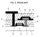
- As shown in Fig. 5, the ferroelectric non-volatile semiconductor memory device comprises a
semiconductor substrate 1,access transistor 2 formed on thesemiconductor substrate 1,source region 3 of theaccess transistor 2, first interlayerinsulating film 4, second interlayerinsulating film 5,bit line 6 electrically connected to thesource region 3 through a contact hole provided on the first interlayerinsulating film 4 and secondinterlayer insulating film 5, andferroelectric capacitor 9 electrically connected to adrain region 7 of theaccess transistor 2 by aplug 8. Aferroelectric film 11 is formed on abottom electrode 10 for theferroelectric capacitor 9, and aside wall 12 made of an insulating film is provided at the side of thebottom electrode 10 andferroelectric film 11. Atop electrode 13 is formed over theferroelectric film 11 andside wall 12 in a way to directly cover them. - However, in the prior art, the
side wall 12 is formed by etching thebottom electrode 10 andferroelectric film 11 of theferroelectric capacitor 9, and then depositing an insulating film, which will become theside wall 12, over the entire surface by means of the CVD (chemical vapor deposition) method. The entire surface of this insulating film is then etched anisotropically to form theside wall 12 at the side of thebottom electrode 10 andferroelectric film 11. - With the above method, however, the entire surface of the
ferroelectric film 11, which is made of a metal oxide material, is damaged by the anisotropic etching, causing significant irregularity in the composition or disorder in the crystal structure. - Another point is that if a SrBi2Ta2O9 film is used for the
ferroelectric film 11 and a silicon oxide film is used for theside wall 12 which is the insulating film, and if the silicon oxide film is etched anisotropically using an etching gas such as CF4, the surface of the SrBi2Ta2O9 film, which is theferroelectric film 11, is exposed after anisotropic etching, but silicon oxide film may remain on theferroelectric film 11. - If the silicon oxide film remains on the
ferroelectric film 11, the structure of the ferroelectric capacitor becomes thetop electrode 13, silicon oxide film,ferroelectric film 11, andbottom electrode 10, instead of the intended structure of thetop electrode 13,ferroelectric film 11, andbottom electrode 10. Voltage applied between thetop electrode 13 andbottom electrode 10 is also distributed to the remaining silicon oxide film connected in series to theferroelectric film 11. This reduces the voltage applied to theferroelectric film 11, causing reduction of residual electric charge, a defect in its characteristics, due to insufficient polarization inversion of theferroelectric film 11. - To prevent any silicon oxide film remaining on the
ferroelectric film 11, over-etching, taking into account the deviation of the etching rate of the silicon oxide film inside the wafer surface and deviation of deposited amount of the silicon oxide film inside the wafer surface, may be required when etching the silicon oxide film. - It has been experimentally confirmed that over-etching causes an oxygen deficit because the entire surface of the SrBi2Ta2O9 film, the
ferroelectric film 11, is exposed to the etching plasma directed at the silicon oxide film. Furthermore, a deficit of the main constitutional atoms of theferroelectric film 11, such as Bi and Ta, is observed. - Such damage may not be recoverable by post-processing such as heat treatment, and would appear to prevent the formation of a ferroelectric capacitor with good electrical characteristics. Consequently, it may be difficult to manufacture a highly reliable ferroelectric non-volatile semiconductor memory device.
- A semiconductor device having a capacitance element including a top electrode, an insulating film and a bottom electrode, said semiconductor device comprising: a passivation film for said insulating film between said insulating film and said top electrode; and a side wall formed at least at the side of said insulating film and said passivation film for said insulating film.
- A semiconductor device having a capacitance element including an insulating film made of a ferroelectric film between a top electrode and a bottom electrode, said semiconductor device comprising: a passivation film for said ferroelectric film between said ferroelectric film and said top electrode; and a side wall formed at least at the side of said ferroelectric film and said passivation film for said ferroelectric film.
- This configuration prevents the surface of the ferroelectric film from being exposed to plasma and damaged during formation of the side wall because the passivation film for ferroelectric film covers the surface of the ferroelectric film. Accordingly, deterioration in electrical characteristics of the ferroelectric film may be eliminated, resulting in a ferroelectric capacitor with good ferroelectric and insulation characteristics.
- In addition, even if the first top electrode as a passivation film for ferroelectric film is damaged during formation of the side wall, the second top electrode formed on the first top electrode will prevent any deterioration in electrode performance.
-
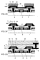
- Fig. 1 is a schematic cross-sectional view of a semiconductor device in accordance with a preferred embodiment of the present invention.
- Figs. 2A to 2G are schematic cross-sectional views of the process flow sequence for manufacturing the semiconductor device in accordance with the preferred embodiment of the present invention.
- Fig. 3 is a comparison graph illustrating the hysteresis characteristics of a ferroelectric capacitor in the semiconductor device in accordance with the preferred embodiment of the present invention and a conventional semiconductor device.
- Fig. 4 is a comparison graph illustrating the current-voltage characteristics of the ferroelectric capacitor in the semiconductor device in accordance with the preferred embodiment of the present invention and the conventional semiconductor device.
- Fig. 5 is a schematic cross-sectional view of a part of the conventional semiconductor device.
-
- A preferred embodiment of a semiconductor device in accordance with a preferred embodiment of the present invention is described with reference to drawings.
- Fig. 1 shows a schematic cross-sectional view of a relevant part of the semiconductor device in the preferred embodiment of the present invention. Figs. 2A to 2G are schematic cross-sectional views of the process flow sequence illustrating a method for manufacturing the semiconductor device in the preferred embodiment of the present invention.
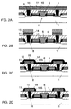
- As shown in Fig. 2A, an
access transistor 2 is formed on asemiconductor substrate 1 as an integrated circuit, and then abit line 6 typically made of a polycide film is formed. A first interlayerinsulating film 4 made of a material such as BPSG is formed on theaccess transistor 2 andbit line 6. Then, a contact hole is formed at a specified area on the firstinterlayer insulating film 4. Aplug 8 is provided in the contact hole to electrically connect theaccess transistor 2 and a ferroelectric capacitor 9 (Fig. 1). Theplug 8 is formed by embedding polysilicon or tungsten in the contact hole and then removing the polysilicon or tungsten deposited outside the contact hole by the etch-back method or chemical mechanical method. - A
bottom electrode 10, constituted of an approximately 200 nm thick multi-layered film formed by successively depositing an adhesion layer, barrier metal, and Pt, is formed over the entire surface of the wafer. Then, a layer approximately 150 nm thick of aferroelectric film 11 made of SrBi2Ta2O9 is formed by the spin coating or CVD method. An approximately 50 nm thickfirst top electrode 14 made of multi-layer metal containing of Pt is deposited. - As shown in Fig. 2B, the first
top electrode 14,ferroelectric film 11, andbottom electrode 10 are dry-etched by mixed gas such as Ar and Cl, using a bottomelectrode processing mask 15 made for example of photo resist. These are all processed into approximately the same shape to form the ferroelectric capacitor 9 (Fig. 1). - Then, as shown in Fig. 2C, after removing the bottom
electrode processing mask 15, made for example of photo resist, typically by ashing, an approximately 300 nm thickinsulating film 16 for aside wall 16S made typically of silicon oxide film is formed over the entire wafer surface. - As shown in Fig. 2D, the entire surface of the
insulating film 16 for theside wall 16S formed on the entire surface of the wafer is etched anisotropically using etching gas such as CF4 to complete theside wall 16S. - The key point here is that the surface of the
ferroelectric film 11 is not exposed to plasma during anisotropic etching of theinsulating film 16 for theside wall 16S because the firsttop electrode 14 covers the surface of theferroelectric film 11 as a passivation film for the ferroelectric film. Accordingly, the surface of theferroelectric film 11 is not damaged, and this preserves the good electrical characteristics of theferroelectric film 11. - As shown in Fig. 2E, a 100 nm thick second
top electrode 17 made typically of Pt is deposited over the entire surface of the wafer, and then a topelectrode processing mask 18, made typically of photo resist, is formed. The secondtop electrode 17 may be formed after the firsttop electrode 14 is etched off In this case however the firsttop electrode 14 does not work as a passivation film for the ferroelectric film. - As shown in Fig. 2F, the second
top electrode 17 is formed using the topelectrode processing mask 18 made typically of photo resist by dry etching with mixed gas such as Ar and Cl. The secondtop electrode 17 is formed to cover the entire firsttop electrode 14 on theferroelectric film 11, or is formed to cover the firsttop electrode 14 on theferroelectric film 11 and the side wall 16s in a way to cover the entire surface. And this secondtop electrode 17 is also formed in a way to be thicker compared to the firsttop electrode 14. This completes theferroelectric capacitor 9. The reason why the thickness of the firsttop electrode 14 can be thinner than the thickness of the secondtop electrode 17 is that the firsttop electrode 14 should have such a thickness that the surface of theferroelectric film 11 is not damaged in the process of the anisotropic etching. - Lastly, as shown in Fig. 2G, a second
interlayer insulating film 5 is formed on thesemiconductor substrate 1 having thisferroelectric capacitor 9.Inter-connection 19, made for example of Al film, formed on the secondinterlayer insulating film 5 reaches the secondtop electrode 17 andbit line 6 through the contact hole formed at a specified area of the secondinterlayer insulating film 5. Asilicon nitride film 20 is formed as a final passivation film, completing the construction of the ferroelectric non-volatile semiconductor memory device. - Fig. 3 shows the hysteresis characteristics of the ferroelectric capacitor used in the ferroelectric non-volatile semiconductor memory device in the preferred embodiment (Curve a) compared with that used in the conventional ferroelectric non-volatile semiconductor memory device (Curve b).
- The data measuring method used in Fig. 3 is the Sawyer-Tower circuit method for example: a pulse of an appropriate electric field is applied between the top and bottom electrodes of the ferroelectric capacitor to evaluate its hysteresis characteristics in accumulated electric charge against applied electric field.
- Fig. 3 shows the measurement results when an electric field of 150 kV/cm to -150 kV/cm is applied to the ferroelectric capacitor. It is apparent from Fig. 3 that, for a ferroelectric non-volatile semiconductor memory device using a conventional ferroelectric capacitor, the difference in accumulated electric charge is 11 µC/cm2 when the applied electric field is 0 kV/cm. For the ferroelectric non-volatile semiconductor memory device using the ferroelectric capacitor in the preferred embodiment of the present invention, the difference in accumulated electric charge is the much improved value of 22 µC/cm2. Accordingly, the hysteresis characteristics of the ferroelectric capacitor in the preferred embodiment of the present invention result in a larger accumulated electric charge than that of the conventional ferroelectric capacitor, giving the preferred embodiment of the present invention significantly better memory characteristics.
- Fig 4 shows a comparison of the current-voltage characteristics of ferroelectric capacitors. Curve c in Fig. 4 illustrates the current-voltage characteristics of the ferroelectric non-volatile semiconductor memory device in the preferred embodiment, and Curve d shows the current-voltage characteristics of the conventional ferroelectric non-volatile semiconductor memory device.
- In Fig. 4, data is measured by applying voltages ranging from 0 V to 6 V between the top and bottom electrodes of the ferroelectric capacitor, and measuring the current flowing through the ferroelectric capacitor to evaluate its current-voltage characteristics.
- It is apparent from Fig. 4 that the current flowing through the ferroelectric capacitor exceeds 10-3 A/cm2 when the conventional ferroelectric non-volatile semiconductor memory device is used. When the ferroelectric non-volatile semiconductor memory device in the preferred embodiment of the present invention is used, current flowing through the ferroelectric capacitor is a maximum of 10-6 A/cm2 . This indicates that the leak current under applied voltage is extremely low, demonstrating the good insulation performance of the ferroelectric film.
- In the preferred embodiment, the
ferroelectric film 11 is used as an insulating film between thetop electrodes bottom electrode 10. The good insulation characteristics can also be obtained by using an ordinary insulating film made of SiO2 film and the like. - In the preferred embodiment, SrBi2Ta2O9 is used for the
ferroelectric film 11. The same effect is also achievable by using SrBi2Nb2O9, which substitutes Nb for Ta; a mixture of both materials, or different compound ratio of Sr, Bi, and Ta can also be used. Other ferroelectric materials such as a PZT film are also applicable for achieving the same effect. - For the
ferroelectric film 11, a ferroelectric film having a bismuth layer perovskite structure is preferable. - The preferred embodiment describes the case when the
bit line 6 is formed at a lower layer than theferroelectric capacitor 9. The same effect is achievable with a structure comprising thebit line 6 formed at a layer above theferroelectric capacitor 9. - In the preferred embodiment, a multi-layered film deposited in the order of adhesion layer, barrier metal, and Pt is used for the
bottom electrode 10. The same effect is achievable by using at least Pt or a multi-layered film containing Pt and iridium oxide. - The preferred embodiment employs Pt for the first
top electrode 14 and secondtop electrode 17. The same effect is also achievable by using at least Pt or a multi-layered film of Pt and iridium oxide. - The preferred embodiment illustrates an example, as shown in Figs. 1 and 2G, where the inter-connection 19 made typically of Al film is connected to the second
top electrode 17 at a single point. Since the secondtop electrode 17 electrically connects to more than oneferroelectric capacitor 9, theinter-connection 19 is connected to more than oneferroelectric capacitors 9 if the inter-connection 19 is connected to the secondtop electrode 17 at a single point. However, the inter-connection 19 can be also connected to the secondtop electrode 17 at more than one point. - Thickness ranges in the present invention are not limited to those described in the above preferred embodiment. The following ranges are preferable.
- Thickness of the bottom electrode 10: 50 nm - 300 nm
- Thickness of the
ferroelectric film 11 made of SrBi2Ta2O9: 50 nm -300 nm - Thickness of the first
top electrode 14 made of Pt: 20 nm - 100 nm - Thickness of the insulating
film 16 for theside wall 16S made typically of silicon oxide film: 100 nm - 500 nm - Thickness of the second
top electrode 17 made typically of Pt: 50 nm - 300 nm - As described above, the first top electrode covers the surface of the ferroelectric film in the present invention. This prevents the surface of the ferroelectric film from being exposed to plasma and damaged during anisotropic etching of the insulating film to form the side wall.
- Accordingly, the present invention offers a ferroelectric capacitor with good ferroelectric and insulation characteristics without degrading the electrical characteristics of the ferroelectric film. This enables the formation of a highly reliable ferroelectric non-volatile semiconductor memory device.
-
- 1
- semiconductor substrate
- 2
- access transistor
- 3
- source region
- 4
- first interlayer insulating film
- 5
- second interlayer insulating film
- 6
- bit line
- 7
- drain region
- 8
- plug
- 9
- ferroelectric capacitor
- 10
- bottom electrode
- 11
- ferroelectric film
- 14
- first top electrode
- 16
- insulating film for side wall
- 16S
- side wall
- 17
- second top electrode
- 19
- inter-connection
- 20
- passivation film
Claims (10)
- A semiconductor device having a capacitance element including a top electrode, an insulating film and a bottom electrode, said semiconductor device comprising:a passivation film for said insulating film between said insulating film and said top electrode;and a side wall formed at least at the side of said insulating film and said passivation film for said insulating film.
- A semiconductor device having a capacitance element including an insulating film made of a ferroelectric film between a top electrode and a bottom electrode, said semiconductor device comprising:a passivation film for said ferroelectric film between said ferroelectric film and said top electrode;and a side wall formed at least at the side of said ferroelectric film and said passivation film for said ferroelectric film.
- The semiconductor device as defined in Claim 2, wherein said passivation film for said ferroelectric film is made of conductive material.
- The semiconductor device as defined in Claim 3, wherein said passivation film for said ferroelectric film is made of the same material as said top electrode.
- The semiconductor device as defined in Claim 4, wherein said top electrode is a multi-layered film including Pt or Pt and iridium oxide.
- The semiconductor device as defined in Claim 2, wherein said ferroelectric film has a bismuth layer perovskite structure.
- A method for manufacturing a semiconductor device, comprising the steps of:forming a bottom electrode, a ferroelectric film and a passivation film for said ferroelectric film into a specified shape;forming a side wall at least at the side of said ferroelectric film and said passivation film for said ferroelectric film by anisotropic etching; andforming a top electrode on said side wall and passivation film for said ferroelectric film.
- The method for manufacturing semiconductor devices as defined in Claim 7, wherein the step of forming a bottom electrode, a ferroelectric film and a passivation film for said ferroelectric film into a specified shape comprising the steps of:forming said bottom electrode;depositing a ferroelectric film and a passivation film for said ferroelectric film sequentially on said bottom electrode; andpatterning said bottom electrode, said ferroelectric film and said passivation film for said ferroelectric film into substantially the same shape.
- A method for manufacturing semiconductor device comprising the steps of:forming a first insulating film on a substrate fabricated with semiconductor integrated circuit;forming a plug connected to a source region or a drain region of said semiconductor integrated circuit, in a contact hole formed at a specified area of said first insulating film;forming a bottom electrode connected to said plug;forming a ferroelectric film and a passivation film for said ferroelectric film into a specified shape on said bottom electrode;forming a side wall at the side of said ferroelectric film and said passivation film for said ferroelectric film by anisotropic etching;and forming a top electrode on said side wall and said passivation film for said ferroelectric film.
- The method for manufacturing semiconductor device as defined in Claim 9, after said step of forming a side wall at the side of said ferroelectric film and said passivation film for said ferroelectric film by anisotropic etching, said method further comprising the steps of;removing the remains of etching on the surface of said passivation film for said ferroelectric film before forming a top electrode on said side wall and said passivation film for said ferroelectric film.
Applications Claiming Priority (2)
| Application Number | Priority Date | Filing Date | Title |
|---|---|---|---|
| JP22393398 | 1998-08-07 | ||
| JP22393398 | 1998-08-07 |
Publications (2)
| Publication Number | Publication Date |
|---|---|
| EP0978881A2 true EP0978881A2 (en) | 2000-02-09 |
| EP0978881A3 EP0978881A3 (en) | 2000-03-29 |
Family
ID=16805990
Family Applications (1)
| Application Number | Title | Priority Date | Filing Date |
|---|---|---|---|
| EP99114608A Withdrawn EP0978881A3 (en) | 1998-08-07 | 1999-07-26 | Ferroelectric capacitor and its manufacturing method |
Country Status (4)
| Country | Link |
|---|---|
| EP (1) | EP0978881A3 (en) |
| KR (1) | KR20000017148A (en) |
| CN (1) | CN1244730A (en) |
| TW (1) | TW419811B (en) |
Cited By (3)
| Publication number | Priority date | Publication date | Assignee | Title |
|---|---|---|---|---|
| EP1151475A1 (en) * | 1999-01-11 | 2001-11-07 | Symetrix Corporation | Ferrolectric memory with ferroelectric thin film and method of fabrication |
| WO2002082549A1 (en) * | 2001-04-05 | 2002-10-17 | Renesas Technology Corp. | Semiconductor integrated circuit device and its manufacturing method |
| DE10116875A1 (en) * | 2001-04-04 | 2002-10-17 | Infineon Technologies Ag | Production of an integrated ferroelectric storage device comprises depositing an intermediate oxide, forming ferroelectric capacitor module on intermediate oxide, structuring, and depositing hydrogen diffusion barrier on structured module |
Families Citing this family (4)
| Publication number | Priority date | Publication date | Assignee | Title |
|---|---|---|---|---|
| KR100389033B1 (en) * | 2001-04-11 | 2003-06-25 | 삼성전자주식회사 | Ferroelectric memory device and fabrication method thereof |
| CN100380668C (en) * | 2002-06-17 | 2008-04-09 | 株式会社东芝 | Semiconductor device having ferroelectric film and manufacturing method thereof |
| KR100870178B1 (en) * | 2005-08-10 | 2008-11-25 | 삼성전자주식회사 | Semiconducotr devices having a metal-insulator-metal capacitor and methods of fabricating the same |
| KR100755373B1 (en) | 2006-09-15 | 2007-09-04 | 삼성전자주식회사 | Contact structure having conductive oxide, ferroelectric random access memory device employing the same and methods of fabricating the same |
Citations (3)
| Publication number | Priority date | Publication date | Assignee | Title |
|---|---|---|---|---|
| US5371700A (en) * | 1992-10-19 | 1994-12-06 | Sharp Kabushiki Kaisha | Semiconductor memory device with covered sidewall spacers |
| US5539613A (en) * | 1992-06-08 | 1996-07-23 | Nec Corporation | Compact semiconductor device including a thin film capacitor of high reliability |
| JPH09116123A (en) * | 1995-10-20 | 1997-05-02 | Sony Corp | Ferroelectric nonvolatile semiconductor storage device |
-
1999
- 1999-06-30 TW TW088111108A patent/TW419811B/en not_active IP Right Cessation
- 1999-07-26 EP EP99114608A patent/EP0978881A3/en not_active Withdrawn
- 1999-08-03 CN CN99111976A patent/CN1244730A/en active Pending
- 1999-08-06 KR KR1019990032316A patent/KR20000017148A/en not_active Application Discontinuation
Patent Citations (3)
| Publication number | Priority date | Publication date | Assignee | Title |
|---|---|---|---|---|
| US5539613A (en) * | 1992-06-08 | 1996-07-23 | Nec Corporation | Compact semiconductor device including a thin film capacitor of high reliability |
| US5371700A (en) * | 1992-10-19 | 1994-12-06 | Sharp Kabushiki Kaisha | Semiconductor memory device with covered sidewall spacers |
| JPH09116123A (en) * | 1995-10-20 | 1997-05-02 | Sony Corp | Ferroelectric nonvolatile semiconductor storage device |
Non-Patent Citations (1)
| Title |
|---|
| PATENT ABSTRACTS OF JAPAN vol. 1997, no. 9, 30 September 1997 (1997-09-30) & JP 09 116123 A (SONY CORP), 2 May 1997 (1997-05-02) * |
Cited By (4)
| Publication number | Priority date | Publication date | Assignee | Title |
|---|---|---|---|---|
| EP1151475A1 (en) * | 1999-01-11 | 2001-11-07 | Symetrix Corporation | Ferrolectric memory with ferroelectric thin film and method of fabrication |
| DE10116875A1 (en) * | 2001-04-04 | 2002-10-17 | Infineon Technologies Ag | Production of an integrated ferroelectric storage device comprises depositing an intermediate oxide, forming ferroelectric capacitor module on intermediate oxide, structuring, and depositing hydrogen diffusion barrier on structured module |
| DE10116875B4 (en) * | 2001-04-04 | 2006-06-14 | Infineon Technologies Ag | Method for producing an integrated ferroelectric memory |
| WO2002082549A1 (en) * | 2001-04-05 | 2002-10-17 | Renesas Technology Corp. | Semiconductor integrated circuit device and its manufacturing method |
Also Published As
| Publication number | Publication date |
|---|---|
| TW419811B (en) | 2001-01-21 |
| KR20000017148A (en) | 2000-03-25 |
| EP0978881A3 (en) | 2000-03-29 |
| CN1244730A (en) | 2000-02-16 |
Similar Documents
| Publication | Publication Date | Title |
|---|---|---|
| US6642563B2 (en) | Semiconductor memory including ferroelectric gate capacitor structure, and method of fabricating the same | |
| US6730951B2 (en) | Capacitor, semiconductor memory device, and method for manufacturing the same | |
| US6753566B2 (en) | Semiconductor device with an oxygen diffusion barrier layer formed from a composite nitride | |
| US7223614B2 (en) | Method for manufacturing semiconductor device, and semiconductor device | |
| US6399974B1 (en) | Semiconductor memory device using an insulator film for the capacitor of the memory cell and method for manufacturing the same | |
| US20060175645A1 (en) | Semiconductor device and its manufacturing method | |
| EP0817259A2 (en) | Thin film capacitor with resistance measuring element | |
| US6887752B2 (en) | Semiconductor memory and process for fabricating the same | |
| US20040115881A1 (en) | Method for fabricating capacitor of semiconductor device | |
| JP2003068993A (en) | Semiconductor device and its manufacturing method | |
| KR100714467B1 (en) | Barrier for capacitor over plug structures | |
| JP3643091B2 (en) | Semiconductor memory device and manufacturing method thereof | |
| US20040089891A1 (en) | Semiconductor device including electrode or the like having opening closed and method of manufacturing the same | |
| EP0978881A2 (en) | Ferroelectric capacitor and its manufacturing method | |
| US6724026B2 (en) | Memory architecture with memory cell groups | |
| KR100668881B1 (en) | Capacitor and method of its manufacture | |
| US7527984B2 (en) | Semiconductor device | |
| JP4002882B2 (en) | Capacitor element, semiconductor memory device and manufacturing method thereof | |
| EP1061582A2 (en) | Capacitor and method of fabricating the same | |
| JP3967315B2 (en) | Capacitor element, semiconductor memory device and manufacturing method thereof | |
| JP2000114489A (en) | Semiconductor device and manufacture thereof | |
| JP2005011866A (en) | Semiconductor device and its manufacturing method |
Legal Events
| Date | Code | Title | Description |
|---|---|---|---|
| PUAI | Public reference made under article 153(3) epc to a published international application that has entered the european phase |
Free format text: ORIGINAL CODE: 0009012 |
|
| AK | Designated contracting states |
Kind code of ref document: A2 Designated state(s): DE NL |
|
| AX | Request for extension of the european patent |
Free format text: AL;LT;LV;MK;RO;SI |
|
| PUAL | Search report despatched |
Free format text: ORIGINAL CODE: 0009013 |
|
| AK | Designated contracting states |
Kind code of ref document: A3 Designated state(s): AT BE CH CY DE DK ES FI FR GB GR IE IT LI LU MC NL PT SE |
|
| AX | Request for extension of the european patent |
Free format text: AL;LT;LV;MK;RO;SI |
|
| 17P | Request for examination filed |
Effective date: 20000606 |
|
| AKX | Designation fees paid |
Free format text: DE NL |
|
| RAP1 | Party data changed (applicant data changed or rights of an application transferred) |
Owner name: MATSUSHITA ELECTRIC INDUSTRIAL CO., LTD. |
|
| STAA | Information on the status of an ep patent application or granted ep patent |
Free format text: STATUS: THE APPLICATION HAS BEEN WITHDRAWN |
|
| 18W | Application withdrawn |
Withdrawal date: 20010725 |