EP0964338B1 - Method and apparatus for operating on a memory unit via a JTAG port - Google Patents
Method and apparatus for operating on a memory unit via a JTAG port Download PDFInfo
- Publication number
- EP0964338B1 EP0964338B1 EP99110882A EP99110882A EP0964338B1 EP 0964338 B1 EP0964338 B1 EP 0964338B1 EP 99110882 A EP99110882 A EP 99110882A EP 99110882 A EP99110882 A EP 99110882A EP 0964338 B1 EP0964338 B1 EP 0964338B1
- Authority
- EP
- European Patent Office
- Prior art keywords
- data
- memory unit
- jtag
- shift register
- ready
- Prior art date
- Legal status (The legal status is an assumption and is not a legal conclusion. Google has not performed a legal analysis and makes no representation as to the accuracy of the status listed.)
- Expired - Lifetime
Links
Images

Classifications
-
- G—PHYSICS
- G06—COMPUTING; CALCULATING OR COUNTING
- G06F—ELECTRIC DIGITAL DATA PROCESSING
- G06F9/00—Arrangements for program control, e.g. control units
- G06F9/06—Arrangements for program control, e.g. control units using stored programs, i.e. using an internal store of processing equipment to receive or retain programs
- G06F9/22—Microcontrol or microprogram arrangements
- G06F9/24—Loading of the microprogram
Definitions
- JTAG Joint Text Action Group
- Memory units are very common in many different types of products. All memory units are programmable but the types of memory units differ in whether or not and how they are erased. Read only memory (ROM) units are not erasable and require replacement if the information programmed therein must be changed. Erasable programmable, read only memory (EPROM) units use electrical signals to program them but require ultraviolet light to erase the entire chip at once. Electrically erasable programmable, read only memory (EEPROM) units and FLASH EEPROM units use electrical signals for erasing and for programming. Thus, a single bit or a single word can be changed if desired.
- ROM Read only memory
- EPROM Erasable programmable, read only memory
- EEPROM Electrically erasable programmable, read only memory
- FLASH EEPROM units use electrical signals for erasing and for programming. Thus, a single bit or a single word can be changed if desired.
- memory units include programmable logic devices (PLDs) which, instead of storing data as do memory units, store logical equations.
- PLDs programmable logic devices
- a PLD can be based on any of the memory unit types.
- the unit To reprogram a programmable memory unit, the unit must be placed into a programming device which erases the unit in the appropriate manner and then electrically programs the unit. For memory units formed in a chip which is connected to a circuit board via a socket, this is not a problem since the units are typically removable from the socket.
- ISP In-system programming
- IEEE Standard 1149.1 defines a test access port, known as a "JTAG port", through which in-system programming occurs using a serial channel.
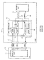
- Figs. 1A and 1B illustrate the JTAG port and its operation.
- Fig. 1A illustrates a personal computer (PC) 10 having a parallel port 11 which controls a chip 12 having a JTAG port 14 while
- Fig. 1B illustrates the method of operation, in the form of a state machine, through the JTAG port 14.
- the chip 12 In order to operate with a JTAG port, the chip 12 must also have a JTAG controller 16 which converts the serial data transmitted through the port to the parallel format needed for accessing the memory unit, labeled 18, via a parallel bus 20.
- the bus can either be a single bus for data and address signals or two busses, one for data signals and one for address signals.
- the JTAG controller 16 decodes the instructions sent to into control signals for controlling the operation of the memory unit 18. These control signals are provided to the memory unit 18 via a control bus 29.
- the JTAG port 14 has four pins, one each for the clock signal TCK, a control signal TMS, a data in signal TDI and a data out signal TDO, and the JTAG controller 16 includes a state machine 22, a data shift register 24, an instruction shift register 27 and an instruction decoder 28.
- the data in signal TDI is a serial presentation of the data and address information to be provided to the memory unit 18 as well as of the instructions to the memory unit 18.
- the data and address information is provided to data shift register 24 which shifts in the serial data provided by signal TDI.
- the data shift register 24 thus has enough storage units to hold both data (typically of 8 bits) and address (typically of 16 bits).
- the instructions are provided to the instruction shift register 27.
- the PC 10 provides the clock signal TCK and the control signal TMS to the state machine 22 which, in turn, controls the operation of the JTAG controller 16. Accordingly, the PC 10 also drives the data in signal TDI and monitors the data out signal TDO.
- the various instructions forming the control signal TMS are indicated in Fig. 1B. As the operation of the JTAG controller 16 is fully defined in the IEEE standard 1149.1, the following discussion will only highlight portions of the operation.
- PC 10 then waits a predetermined length of time T, as defined for each type of operation, before transmitting the next series of data and address bits.
- T a predetermined length of time
- the length of time is set to ensure that the desired operation finishes before the next set of data is shifted in.
- the timing is shown in Fig. 1C for two bytes, labeled BYTE 0 and BYTE 1.
- the shifting operation for BYTE 0, as indicated by the data in TDI signal, occurs first, during which the 24 data and address bits are shifted into data shift register 24 and 24 blank bits are shifted out to data out signal TDO.
- the state machine 22 moves to the UPDATE state 42 after which the state machine moves to the run-test/idle state 44 in which an R-T-I pulse 45 is generated.
- the memory unit 18 then performs the operation, as indicated by the OPERATION signal.
- the OPERATION signal returns to its non-active state well within the period of length T allotted to it.
- the process repeats itself with the next shift operation, for BYTE 1, during which the data of BYTE 0 is shifted out to data out signal TDO.
- US 5,423,050 discloses a system for extending the time T in which a device can respond on the JTAG bus by providing a "ready" signal to indicate that a device cannot respond within the default access time. However, this does not disclose a technique for reducing the operation time.
- An object of the present invention is to provide a novel method of controlling the operation of an on-chip memory unit through a JTAG port.
- the method of controlling the operations of an on-chip memory unit includes the steps of receiving an indication at least of a ready or busy state of said memory unit; instructing said memory unit to perform the next operation once the indication is of the ready state; and wherein said step of receiving includes the steps of capturing and placing in a shift register said indication and data and address information of the previous byte provided to said memory unit and shifting in data and address information of a next byte and at least one extra bit through the shift register such that said indication is also shifted out of said shift register to a data out pin of a JTAG port, said steps of capturing and shifting repeating until said indication is of the ready state.
- the method further includes the step of shifting the data and address information of the next byte to be provided to the memory unit into a shift register while the memory unit performs the operation.
- a memory chip which includes a memory unit having a ready / busy output line; a JTAG port for communicating with an external processor and having JTAG input and JTAG output lines; and a JTAG controller for controlling the operations of said memory unit in accordance with instructions from said external processor received via said JTAG port, the JTAG controller comprising: a shift register having an input connected to said JTAG input line and an output connected to said JTAG output line and having a plurality of storage elements one of which is connected to said ready / busy output line and a multiplicity of which are available for receiving data and address information of a byte of said memory unit from said JTAG input line; a buffer for receiving said data and address information from said shift register and for providing such to said memory unit; and a state machine for controlling the operation of said shift register and buffer under instruction from said external processor and for instructing said memory unit to perform the next operation once the ready / busy output line indicates the ready state.
- a system comprising the memory chip and a processor arranged to communicate with the JTAG port of the memory chip.
- the memory unit typically has an "end-of-execution” or “ready/busy” (RDY/BSY) signal which indicates whether or not the memory unit is in the desired mode.
- RY/BSY ready/busy signal
- the present invention shifts in the data and address bits for the next bit while the memory unit performs the desired operation. This double buffering adds to the speed gain of the present invention.
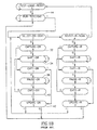
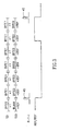
- Fig. 2 illustrates the system of the present invention.
- the chip 50 includes memory unit 18, a JTAG controller 52, constructed and operative in accordance with a preferred embodiment of the present invention, and a JTAG port 14.
- Fig. 2 shows a "ready/busy" (RDY/BSY) output line 59 of memory unit 18.
- Fig. 2 shows the operation with PC 10; it will be appreciated that the operation described hereinbelow can occur with any external processor of which PC 10 is only an example.
- Other types of processors include programmers and automatic tester equipment.
- the JTAG controller 52 includes state machine 22, a buffer 57 and a data shift register, labeled 56.
- Data shift register 56 typically has at least one extra storage unit 58 more than the number of storage units needed to store the data and address bits.
- Extra storage unit 58 is connected to the RDY/BSY line 59 and thus, can receive the current state of the RDY/BSY signal.
- the present discussion will assume only one extra storage unit 58. It will be appreciated that additional extra storage units can be included for capturing other information from the internal blocks of the chip 50.
- the JTAG controller 52 On each cycle to input the address and data information, the JTAG controller 52 first captures (state 32 of Fig. 1B) the current value of the RDY/BSY line 59 and the data and address bits currently found on bus 20 and places the captured information into data shift register 56. The JTAG controller 52 then shifts (state 34 of Fig. 1B) the next byte of the data in TDI signal into data shift register 56. This shifting causes the captured data, including the value in the extra storage unit 58 (Fig. 2), to be shifted out as the TDO data out signal. Fig. 2 shows extra storage unit 58 as the last storage unit of the data shift register 56; however, extra storage unit 58 can be placed anywhere within data shift register 56.
- the value of the RDY/BSY signal is periodically provided back to the PC 10.
- the length of time between values of the RDY/BSY signal is a function of the time it takes to shift in all of the data and address bits and to update (state 42) the buffer 57 with the newly shifted in data.
- the RDY/BSY signal is not provided to the buffer 57.
- the PC 10 can begin the next desired operation any time thereafter.
- the data and address bits are then transferred to buffer 57 in the UPDATE state 42.
- the PC 10 checks the value of the RDY/BSY signal. Since the memory unit 18 is ready for an operation, the RDY/BSY signal is in the RDY state and thus, the PC 10 moves to the Run-Test/Idle state 44. In response, JTAG controller 52 generates an R-T-I pulse 45. The desired operation now begins and the RDY/BSY signal becomes busy (BSY) (e.g. for Fig. 3, the RDY/BSY signal becomes low).
- BSY busy
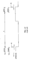
- the PC 10 while the desired operation occurs, the PC 10 continually operates to receive the RDY/BSY status. To do so, the PC 10 first indicates to the JTAG controller 52 to capture the RDY/BSY value and the data and address values currently on the parallel bus 20 into the data shift register 24. PC 10 then shifts in the next byte, BYTE 1, and an extra bit in order to shift out the previous byte, BYTE 0, and the current state of the RDY/BSY signal.
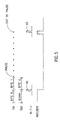
- Fig. 3 shows the repeated shifting in of BYTE 1 and an extra bit in the data in signal TDI and the repeated shifting out of BYTE 0 and RDY or BSY state in the data out signal TDO. This downloading of the next data to be used, while the memory unit is being operated on, is known as "double buffering".
- the PC 10 orders that the buffer 57 be updated and checks the value of the RDY/BSY signal.
- the RDY/BSY signal becomes ready during the fifth shifting in of the next byte, BYTE 1. Since the RDY/BSY signal is captured prior to the shifting in, the value of the RDY/BSY signal after the fifth shifting in will still be BSY. However, after the sixth shifting in of the data, the RDY/BSY signal will be RDY and the PC 10 can then move to the Run-Test/Idle state 44 to begin a new desired operation.
- the next R-T-I pulse 45 is issued as soon as the RDY signal comes out of the JTAG port. This provides significant time savings since the period T is defined as the longest possible time it takes to program or erase a byte of the memory 18 and most desired operations take significantly less time than the maximum.
- the present invention can also be implemented by waiting Q clock pulses of the TCK signal, at the run-test/idle state 44, before capturing and shifting the data, address and RDY/BSY signals.
- Q clock pulses occur in significantly less time than the predetermined length of time T.
- the PC 10 still waits until the RDY/BSY signal indicates that the memory 18 is ready before beginning the desired operation.
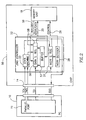
- FIG. 4 illustrates a further alternative embodiment of the present invention in which the RDY/BSY signal is also provided out to a non-JTAG port, labeled 72.
- Fig. 4 shows the details of the PC 10 and chip, labeled 70 and Fig. 5 is a timing diagram of the operation of the system of Fig. 4. Similar reference numerals refer to similar elements.
- the JTAG controller labeled 74, includes state machine 22, buffer 57 and data shift register 24, the shift register without any extra storage units.
- the RDY/BSY signal is provided to one pin of non-JTAG port 72 and this pin is connected to PC 10 via parallel port 11. If desired, the RDY/BSY signal can be provided to an interrupt of the PC 10.
- the data and address for the first byte, BYTE 0 is first shifted into data shift register 24 after which it is updated into buffer 57 and then the R-T-I pulse 45 is issued, causing the RDY/BSY signal to become BSY.
- the data and address of the next byte, BYTE 1 is then shifted through data shift register 24, thereby providing double buffering for this embodiment also.
- the PC 10 moves the state machine 22 to the PAUSE state 38 (Fig. 1B) until the RDY/BSY signal changes to the RDY state, as received directly through port 72. If the RDY/BSY signal is provided to an interrupt of the PC 10, then, as soon as the RDY/BSY signal changes state, the PC 10 will move the state machine 22 out of the PAUSE state 38.
- PC 10 can then move the state machine 22 from PAUSE state 38 to the EXIT2 state 40 to the UPDATE state 42. This is also indicated in Fig. 5 as part of the TDI signal.
- the PC 10 moves to the Run-Test/Idle state 44 and the JTAG controller 74 generates the R-T-I pulse 45.
- the memory unit 18 spends very little time in the RDY state.
- pin 72 can be configured with an open drain and all of the devices can connect their RDY/BSY lines to pin 72. Thus, pin 72 will produce a RDY signal only when all of the devices are ready.
Description
- The present invention relates to Joint Text Action Group (JTAG) ports generally and to their method of operation in particular.
- Memory units are very common in many different types of products. All memory units are programmable but the types of memory units differ in whether or not and how they are erased. Read only memory (ROM) units are not erasable and require replacement if the information programmed therein must be changed. Erasable programmable, read only memory (EPROM) units use electrical signals to program them but require ultraviolet light to erase the entire chip at once. Electrically erasable programmable, read only memory (EEPROM) units and FLASH EEPROM units use electrical signals for erasing and for programming. Thus, a single bit or a single word can be changed if desired.
- Included in the term "memory units" are programmable logic devices (PLDs) which, instead of storing data as do memory units, store logical equations. A PLD can be based on any of the memory unit types.
- To reprogram a programmable memory unit, the unit must be placed into a programming device which erases the unit in the appropriate manner and then electrically programs the unit. For memory units formed in a chip which is connected to a circuit board via a socket, this is not a problem since the units are typically removable from the socket.
- However, those units which are directly soldered to the circuit board and those which are formed within a multi-function chip cannot be removed to the programming device. These units can be operated on (i.e. read, programmed, erased, verified, etc.) via a parallel port.
- In-system programming (ISP) provides a method of operating on an on-chip memory unit, or any non-removable memory unit. IEEE Standard 1149.1 defines a test access port, known as a "JTAG port", through which in-system programming occurs using a serial channel. Figs. 1A and 1B, to which reference is now made, illustrate the JTAG port and its operation. Fig. 1A illustrates a personal computer (PC) 10 having a
parallel port 11 which controls achip 12 having aJTAG port 14 while Fig. 1B illustrates the method of operation, in the form of a state machine, through the JTAGport 14. - In order to operate with a JTAG port, the
chip 12 must also have aJTAG controller 16 which converts the serial data transmitted through the port to the parallel format needed for accessing the memory unit, labeled 18, via aparallel bus 20. The bus can either be a single bus for data and address signals or two busses, one for data signals and one for address signals. In addition, the JTAGcontroller 16 decodes the instructions sent to into control signals for controlling the operation of thememory unit 18. These control signals are provided to thememory unit 18 via acontrol bus 29. - The JTAG
port 14 has four pins, one each for the clock signal TCK, a control signal TMS, a data in signal TDI and a data out signal TDO, and theJTAG controller 16 includes astate machine 22, adata shift register 24, aninstruction shift register 27 and aninstruction decoder 28. - The data in signal TDI is a serial presentation of the data and address information to be provided to the
memory unit 18 as well as of the instructions to thememory unit 18. The data and address information is provided todata shift register 24 which shifts in the serial data provided by signal TDI. Thedata shift register 24 thus has enough storage units to hold both data (typically of 8 bits) and address (typically of 16 bits). The instructions are provided to theinstruction shift register 27. - Via
parallel port 11, the PC 10 provides the clock signal TCK and the control signal TMS to thestate machine 22 which, in turn, controls the operation of theJTAG controller 16. Accordingly, the PC 10 also drives the data in signal TDI and monitors the data out signal TDO. The various instructions forming the control signal TMS are indicated in Fig. 1B. As the operation of the JTAGcontroller 16 is fully defined in the IEEE standard 1149.1, the following discussion will only highlight portions of the operation. - Initially, whatever information is on
bus 20 is captured (state 32) and placed intodata shift register 24. The data and address information of data in signal TDI is then shifted (state 34) intodata shift register 24, causing the captured data to be shifted out, as data out signal TDO. Once a full set of data and address information has been shifted intodata shift register 24, thestate machine 22 indicates (state 42) todata shift register 24 to provide the data toparallel bus 20.State machine 22 then indicates (state 44) to theinstruction decoder 28 to provide the instructions, viacontrol bus 29, tomemory unit 18 to run the desired operation (reading, programming, erasure, verification, etc.) for the address. - PC 10 then waits a predetermined length of time T, as defined for each type of operation, before transmitting the next series of data and address bits. The length of time is set to ensure that the desired operation finishes before the next set of data is shifted in.
- The timing is shown in Fig. 1C for two bytes, labeled
BYTE 0 andBYTE 1. The shifting operation forBYTE 0, as indicated by the data in TDI signal, occurs first, during which the 24 data and address bits are shifted intodata shift register register 24, thestate machine 22 moves to the UPDATEstate 42 after which the state machine moves to the run-test/idle state 44 in which anR-T-I pulse 45 is generated. Thememory unit 18 then performs the operation, as indicated by the OPERATION signal. As noted, the OPERATION signal returns to its non-active state well within the period of length T allotted to it. The process repeats itself with the next shift operation, forBYTE 1, during which the data ofBYTE 0 is shifted out to data out signal TDO. - It will be appreciated that using the JTAG
port 14 to operate on a memory unit is time consuming due to the serial transfer of the data and the long wait until the operation has finished for each byte. - US 5,423,050 discloses a system for extending the time T in which a device can respond on the JTAG bus by providing a "ready" signal to indicate that a device cannot respond within the default access time. However, this does not disclose a technique for reducing the operation time.
- An object of the present invention is to provide a novel method of controlling the operation of an on-chip memory unit through a JTAG port.
- Therefore, in accordance with a preferred embodiment of the present invention, the method of controlling the operations of an on-chip memory unit includes the steps of receiving an indication at least of a ready or busy state of said memory unit; instructing said memory unit to perform the next operation once the indication is of the ready state; and wherein said step of receiving includes the steps of capturing and placing in a shift register said indication and data and address information of the previous byte provided to said memory unit and shifting in data and address information of a next byte and at least one extra bit through the shift register such that said indication is also shifted out of said shift register to a data out pin of a JTAG port, said steps of capturing and shifting repeating until said indication is of the ready state.
- Furthermore, in accordance with a preferred embodiment of the present invention, the method further includes the step of shifting the data and address information of the next byte to be provided to the memory unit into a shift register while the memory unit performs the operation.
- There is also provided, in accordance with a preferred embodiment of the present invention, a memory chip which includes a memory unit having a ready / busy output line; a JTAG port for communicating with an external processor and having JTAG input and JTAG output lines; and a JTAG controller for controlling the operations of said memory unit in accordance with instructions from said external processor received via said JTAG port, the JTAG controller comprising: a shift register having an input connected to said JTAG input line and an output connected to said JTAG output line and having a plurality of storage elements one of which is connected to said ready / busy output line and a multiplicity of which are available for receiving data and address information of a byte of said memory unit from said JTAG input line; a buffer for receiving said data and address information from said shift register and for providing such to said memory unit; and a state machine for controlling the operation of said shift register and buffer under instruction from said external processor and for instructing said memory unit to perform the next operation once the ready / busy output line indicates the ready state.
- According to another aspect of the invention there is provided a system comprising the memory chip and a processor arranged to communicate with the JTAG port of the memory chip.
- The present invention will be understood and appreciated more fully from the following detailed description taken in conjunction with the appended drawings in which:
- Fig. 1A is a schematic illustration of a prior art memory chip and a PC;
- Fig. 1B is a schematic illustration of a state machine useful in the JTAG controller of the prior art;
- Fig. 1C is a timing diagram illustration of the timing of operations through the JTAG port;
- Fig. 2 is a schematic illustration of a memory chip, constructed and operative in accordance with a preferred embodiment of the present invention, and a PC;
- Fig. 3 is a timing diagram illustration of the timing of operations for the memory chip of Fig. 2;
- Fig. 4 is a schematic illustration of a memory chip, constructed and operative in accordance with an alternative preferred embodiment of the present invention, and a PC; and
- Fig. 5 is a timing diagram illustration of the timing of operations for the memory chip of Fig. 4.
- Applicants have realized that the memory unit typically has an "end-of-execution" or "ready/busy" (RDY/BSY) signal which indicates whether or not the memory unit is in the desired mode. The present invention takes advantage of this signal to reduce the amount of time required to operate on the on-chip memory unit using the JTAG port.
- Furthermore, the present invention shifts in the data and address bits for the next bit while the memory unit performs the desired operation. This double buffering adds to the speed gain of the present invention.
- Reference is now made to Fig. 2 which illustrates the system of the present invention. The
chip 50 includesmemory unit 18, aJTAG controller 52, constructed and operative in accordance with a preferred embodiment of the present invention, and aJTAG port 14. In addition, Fig. 2 shows a "ready/busy" (RDY/BSY)output line 59 ofmemory unit 18. - Fig. 2 shows the operation with
PC 10; it will be appreciated that the operation described hereinbelow can occur with any external processor of whichPC 10 is only an example. Other types of processors include programmers and automatic tester equipment. - In accordance with a preferred embodiment of the present invention, the
JTAG controller 52 includesstate machine 22, abuffer 57 and a data shift register, labeled 56.Data shift register 56 typically has at least oneextra storage unit 58 more than the number of storage units needed to store the data and address bits.Extra storage unit 58 is connected to the RDY/BSY line 59 and thus, can receive the current state of the RDY/BSY signal. The present discussion will assume only oneextra storage unit 58. It will be appreciated that additional extra storage units can be included for capturing other information from the internal blocks of thechip 50. - On each cycle to input the address and data information, the
JTAG controller 52 first captures (state 32 of Fig. 1B) the current value of the RDY/BSY line 59 and the data and address bits currently found onbus 20 and places the captured information intodata shift register 56. TheJTAG controller 52 then shifts (state 34 of Fig. 1B) the next byte of the data in TDI signal intodata shift register 56. This shifting causes the captured data, including the value in the extra storage unit 58 (Fig. 2), to be shifted out as the TDO data out signal. Fig. 2 showsextra storage unit 58 as the last storage unit of thedata shift register 56; however,extra storage unit 58 can be placed anywhere withindata shift register 56. - Due to the data shifting, the value of the RDY/BSY signal is periodically provided back to the
PC 10. The length of time between values of the RDY/BSY signal is a function of the time it takes to shift in all of the data and address bits and to update (state 42) thebuffer 57 with the newly shifted in data. However, the RDY/BSY signal is not provided to thebuffer 57. - Once the TDO data out signal receives the RDY/BSY signal which indicates that the
memory unit 18 has finished the desired operation, thePC 10 can begin the next desired operation any time thereafter. - The timing is shown in Fig. 3, to which reference is now made. Initially, the current values of the RDY/BSY signal and of the data and address bits on
parallel bus 20 are captured, after which the data in signal TDI shifts the data and address bits forBYTE 0 and an extra bit intodata shift register 56. X+1 bits are transferred in, where X is the number of data and address bits and the extra bit is needed to "push" out the RDY/BSY value stored in theextra storage register 58. If there are N extra storage registers 58, then X+N bits are transferred in. ForBYTE 0, the data out signal TDO is X blank bits and the RDY value of the RDY/BSY signal. - Once all the data are shifted in and the captured data, including the RDY/BSY value shifted out, the data and address bits are then transferred to buffer 57 in the
UPDATE state 42. During the shifting operation (state 34) thePC 10 checks the value of the RDY/BSY signal. Since thememory unit 18 is ready for an operation, the RDY/BSY signal is in the RDY state and thus, thePC 10 moves to the Run-Test/Idle state 44. In response,JTAG controller 52 generates anR-T-I pulse 45. The desired operation now begins and the RDY/BSY signal becomes busy (BSY) (e.g. for Fig. 3, the RDY/BSY signal becomes low). - In accordance with a preferred embodiment of the present invention, while the desired operation occurs, the
PC 10 continually operates to receive the RDY/BSY status. To do so, thePC 10 first indicates to theJTAG controller 52 to capture the RDY/BSY value and the data and address values currently on theparallel bus 20 into thedata shift register 24.PC 10 then shifts in the next byte,BYTE 1, and an extra bit in order to shift out the previous byte,BYTE 0, and the current state of the RDY/BSY signal. Fig. 3 shows the repeated shifting in ofBYTE 1 and an extra bit in the data in signal TDI and the repeated shifting out ofBYTE 0 and RDY or BSY state in the data out signal TDO. This downloading of the next data to be used, while the memory unit is being operated on, is known as "double buffering". - After each shifting in, the
PC 10 orders that thebuffer 57 be updated and checks the value of the RDY/BSY signal. In the example of Fig. 3, the RDY/BSY signal becomes ready during the fifth shifting in of the next byte,BYTE 1. Since the RDY/BSY signal is captured prior to the shifting in, the value of the RDY/BSY signal after the fifth shifting in will still be BSY. However, after the sixth shifting in of the data, the RDY/BSY signal will be RDY and thePC 10 can then move to the Run-Test/Idle state 44 to begin a new desired operation. - It will be appreciated that, in the present invention, there is no waiting the predefined period T before shifting in the next data and address information. Rather, the
next R-T-I pulse 45 is issued as soon as the RDY signal comes out of the JTAG port. This provides significant time savings since the period T is defined as the longest possible time it takes to program or erase a byte of thememory 18 and most desired operations take significantly less time than the maximum. - The present invention can also be implemented by waiting Q clock pulses of the TCK signal, at the run-test/
idle state 44, before capturing and shifting the data, address and RDY/BSY signals. Q clock pulses occur in significantly less time than the predetermined length of time T. In this embodiment, thePC 10 still waits until the RDY/BSY signal indicates that thememory 18 is ready before beginning the desired operation. - Reference is now made to Figs. 4 and 5 which illustrate a further alternative embodiment of the present invention in which the RDY/BSY signal is also provided out to a non-JTAG port, labeled 72. Fig. 4 shows the details of the
PC 10 and chip, labeled 70 and Fig. 5 is a timing diagram of the operation of the system of Fig. 4. Similar reference numerals refer to similar elements. - As in the prior art, the JTAG controller, labeled 74, includes
state machine 22,buffer 57 anddata shift register 24, the shift register without any extra storage units. However, in this embodiment, the RDY/BSY signal is provided to one pin ofnon-JTAG port 72 and this pin is connected toPC 10 viaparallel port 11. If desired, the RDY/BSY signal can be provided to an interrupt of thePC 10. - As in the previous embodiments and as shown in Fig. 5, the data and address for the first byte,
BYTE 0, is first shifted intodata shift register 24 after which it is updated intobuffer 57 and then theR-T-I pulse 45 is issued, causing the RDY/BSY signal to become BSY. - In accordance with this embodiment of the present invention, the data and address of the next byte,
BYTE 1, is then shifted throughdata shift register 24, thereby providing double buffering for this embodiment also. ThePC 10 moves thestate machine 22 to the PAUSE state 38 (Fig. 1B) until the RDY/BSY signal changes to the RDY state, as received directly throughport 72. If the RDY/BSY signal is provided to an interrupt of thePC 10, then, as soon as the RDY/BSY signal changes state, thePC 10 will move thestate machine 22 out of thePAUSE state 38. - Since the data and address of the next byte,
BYTE 1, is already shifted intodata shift register 24,PC 10 can then move thestate machine 22 fromPAUSE state 38 to theEXIT2 state 40 to theUPDATE state 42. This is also indicated in Fig. 5 as part of the TDI signal. Once the UPDATE has finished (i.e. once the data and address bits are transferred to buffer 57), thePC 10 moves to the Run-Test/Idle state 44 and theJTAG controller 74 generates theR-T-I pulse 45. As can be seen in Fig. 5 and due to the double buffering, thememory unit 18 spends very little time in the RDY state. - If a few devices are to be programmed or erased in parallel,
pin 72 can be configured with an open drain and all of the devices can connect their RDY/BSY lines to pin 72. Thus, pin 72 will produce a RDY signal only when all of the devices are ready. - It will be appreciated by persons skilled in the art that the present invention is not limited by what has been particularly shown and described herein above. Rather the scope of the invention is defined by the claims that follow:
Claims (4)
- A method of controlling the operations of an on-chip memory unit (18), the method comprising the steps of:receiving an indication at least of a ready or busy state of said memory unit (18);instructing said memory unit (18) to perform the next operation once the indication is of the ready state; andwherein said step of receiving includes the steps of capturing and placing in a shift register (56) said indication and data and address information of the previous byte provided to said memory unit (18) and shifting in data and address information of a next byte and at least one extra bit through the shift register (56) such that said indication is also shifted out of said shift register (56) to a data out pin (TDO) of a JTAG port (14), said steps of capturing and shifting repeating until said indication is of the ready state.
- A method according to claim 1 and also comprising the step of shifting the data and address information of the next byte to be provided to said memory unit (18) into a shift register (56) while said memory unit (18) performs said operation.
- A memory chip (50) comprising:a memory unit (18) having a ready / busy output line;a JTAG port (14) for communicating with an external processor (10) and having JTAG input (TDI) and JTAG output (TDO) lines; anda JTAG controller (52) for controlling the operations of said memory unit (18) in accordance with instructions from said external processor (10) received via said JTAG port (14), the JTAG controller comprising:a shift register (56) having an input connected to said JTAG input line (TDI) and an output connected to said JTAG output line (TDO) and having a plurality of storage elements one of which is connected to said ready / busy output line and a multiplicity of which are available for receiving data and address information of a byte of said memory unit (18) from said JTAG input line (TDI);a buffer (57) for receiving said data and address information from said shift register (56) and for providing such to said memory unit (18); anda state machine (22) for controlling the operation of said shift register (56) and buffer (57) under instruction from said external processor (10) and for instructing said memory unit (18) to perform the next operation once the ready / busy output line indicates the ready state.
- A system comprising the memory chip (50) according to claim 3 and a processor (10) arranged to communicate with the JTAG port (14) of the memory chip (50).
Applications Claiming Priority (2)
| Application Number | Priority Date | Filing Date | Title |
|---|---|---|---|
| US09/093,943 US6243842B1 (en) | 1998-06-08 | 1998-06-08 | Method and apparatus for operating on a memory unit via a JTAG port |
| US93943 | 1998-06-08 |
Publications (3)
| Publication Number | Publication Date |
|---|---|
| EP0964338A2 EP0964338A2 (en) | 1999-12-15 |
| EP0964338A3 EP0964338A3 (en) | 2002-04-03 |
| EP0964338B1 true EP0964338B1 (en) | 2007-01-24 |
Family
ID=22241848
Family Applications (1)
| Application Number | Title | Priority Date | Filing Date |
|---|---|---|---|
| EP99110882A Expired - Lifetime EP0964338B1 (en) | 1998-06-08 | 1999-06-07 | Method and apparatus for operating on a memory unit via a JTAG port |
Country Status (4)
| Country | Link |
|---|---|
| US (1) | US6243842B1 (en) |
| EP (1) | EP0964338B1 (en) |
| JP (2) | JP4398008B2 (en) |
| DE (1) | DE69934936D1 (en) |
Families Citing this family (29)
| Publication number | Priority date | Publication date | Assignee | Title |
|---|---|---|---|---|
| US6987382B1 (en) * | 1995-10-31 | 2006-01-17 | Texas Instruments Incorporated | System with functional and selector circuits connected by mode lead |
| JP4475709B2 (en) * | 1999-11-15 | 2010-06-09 | 株式会社ルネサステクノロジ | Microcomputer |
| US6651199B1 (en) * | 2000-06-22 | 2003-11-18 | Xilinx, Inc. | In-system programmable flash memory device with trigger circuit for generating limited duration program instruction |
| US7058856B2 (en) * | 2000-07-18 | 2006-06-06 | Oki Electric Industry Co., Ltd. | Semiconductor circuit with flash ROM and improved security for the contents thereof |
| US6757844B1 (en) * | 2000-10-25 | 2004-06-29 | Cypress Semiconductor Corp. | Architecture and logic to control a device without a JTAG port through a device with a JTAG port |
| KR100394575B1 (en) * | 2001-04-11 | 2003-08-14 | 삼성전자주식회사 | method for outputting internal information through test pin in semiconductor memory and output circuit therefore |
| US6925583B1 (en) * | 2002-01-09 | 2005-08-02 | Xilinx, Inc. | Structure and method for writing from a JTAG device with microcontroller to a non-JTAG device |
| US6983441B2 (en) | 2002-06-28 | 2006-01-03 | Texas Instruments Incorporated | Embedding a JTAG host controller into an FPGA design |
| US20040141518A1 (en) * | 2003-01-22 | 2004-07-22 | Alison Milligan | Flexible multimode chip design for storage and networking |
| US7684624B2 (en) * | 2003-03-03 | 2010-03-23 | Smart Technologies Ulc | System and method for capturing images of a target area on which information is recorded |
| US7137037B2 (en) * | 2003-03-27 | 2006-11-14 | Silicon Motion, Inc. | Data storage system and method for testing the same |
| US6948147B1 (en) * | 2003-04-03 | 2005-09-20 | Xilinx, Inc. | Method and apparatus for configuring a programmable logic device using a master JTAG port |
| US7521960B2 (en) * | 2003-07-31 | 2009-04-21 | Actel Corporation | Integrated circuit including programmable logic and external-device chip-enable override control |
| US7170315B2 (en) | 2003-07-31 | 2007-01-30 | Actel Corporation | Programmable system on a chip |
| US7138824B1 (en) | 2004-05-10 | 2006-11-21 | Actel Corporation | Integrated multi-function analog circuit including voltage, current, and temperature monitor and gate-driver circuit blocks |
| US7099189B1 (en) | 2004-10-05 | 2006-08-29 | Actel Corporation | SRAM cell controlled by non-volatile memory cell |
| US7116181B2 (en) * | 2004-12-21 | 2006-10-03 | Actel Corporation | Voltage- and temperature-compensated RC oscillator circuit |
| US7119398B1 (en) * | 2004-12-22 | 2006-10-10 | Actel Corporation | Power-up and power-down circuit for system-on-a-chip integrated circuit |
| US7446378B2 (en) * | 2004-12-29 | 2008-11-04 | Actel Corporation | ESD protection structure for I/O pad subject to both positive and negative voltages |
| CN100357874C (en) * | 2005-09-30 | 2007-12-26 | 华为技术有限公司 | Flash memory loading method and system based on boundary scan |
| US7505331B1 (en) * | 2005-11-23 | 2009-03-17 | Altera Corporation | Programmable logic device with differential communications support |
| US7451367B2 (en) * | 2006-02-14 | 2008-11-11 | Atmel Corporation | Accessing sequential data in microcontrollers |
| US7610528B2 (en) * | 2006-02-14 | 2009-10-27 | Atmel Corporation | Configuring flash memory |
| US7346820B2 (en) * | 2006-03-23 | 2008-03-18 | Freescale Semiconductor, Inc. | Testing of data retention latches in circuit devices |
| US7617386B2 (en) * | 2007-04-17 | 2009-11-10 | Xmos Limited | Scheduling thread upon ready signal set when port transfers data on trigger time activation |
| US7721163B2 (en) * | 2007-04-23 | 2010-05-18 | Micron Technology, Inc. | JTAG controlled self-repair after packaging |
| US7815059B2 (en) * | 2007-06-27 | 2010-10-19 | John Francis Mulholland | Display rack and method for supporting containerized plants |
| US7908532B2 (en) * | 2008-02-16 | 2011-03-15 | International Business Machines Corporation | Automated system and processing for expedient diagnosis of broken shift registers latch chains |
| US7900106B2 (en) * | 2008-03-28 | 2011-03-01 | Atmel Corporation | Accessing sequential data in a microcontroller |
Citations (2)
| Publication number | Priority date | Publication date | Assignee | Title |
|---|---|---|---|---|
| EP0636976A1 (en) * | 1993-07-28 | 1995-02-01 | Koninklijke Philips Electronics N.V. | Microcontroller provided with hardware for supporting debugging as based on boundary scan standard-type extensions |
| EP0840217A1 (en) * | 1996-10-31 | 1998-05-06 | STMicroelectronics Limited | An integrated circuit with TAP (test access port) controller |
Family Cites Families (9)
| Publication number | Priority date | Publication date | Assignee | Title |
|---|---|---|---|---|
| US4426679A (en) * | 1980-09-29 | 1984-01-17 | Honeywell Information Systems Inc. | Communication multiplexer using a random access memory for storing an acknowledge response to an input/output command from a central processor |
| JPH01118950A (en) * | 1987-10-31 | 1989-05-11 | Toshiba Corp | Bus control system |
| US5355369A (en) * | 1991-04-26 | 1994-10-11 | At&T Bell Laboratories | High-speed integrated circuit testing with JTAG |
| US5423050A (en) * | 1991-11-27 | 1995-06-06 | Ncr Corporation | Intermodule test across system bus utilizing serial test bus |
| US5375222A (en) * | 1992-03-31 | 1994-12-20 | Intel Corporation | Flash memory card with a ready/busy mask register |
| US5485466A (en) * | 1993-10-04 | 1996-01-16 | Motorola, Inc. | Method and apparatus for performing dual scan path testing of an array in a data processing system |
| JPH08278938A (en) * | 1995-04-05 | 1996-10-22 | Hitachi Ltd | Dma device |
| US5768289A (en) * | 1997-05-22 | 1998-06-16 | Intel Corporation | Dynamically controlling the number of boundary-scan cells in a boundary-scan path |
| US6000051A (en) * | 1997-10-10 | 1999-12-07 | Logic Vision, Inc. | Method and apparatus for high-speed interconnect testing |
-
1998
- 1998-06-08 US US09/093,943 patent/US6243842B1/en not_active Expired - Lifetime
-
1999
- 1999-06-03 JP JP15672499A patent/JP4398008B2/en not_active Expired - Lifetime
- 1999-06-07 EP EP99110882A patent/EP0964338B1/en not_active Expired - Lifetime
- 1999-06-07 DE DE69934936T patent/DE69934936D1/en not_active Expired - Lifetime
-
2009
- 2009-06-04 JP JP2009134672A patent/JP4527181B2/en not_active Expired - Lifetime
Patent Citations (2)
| Publication number | Priority date | Publication date | Assignee | Title |
|---|---|---|---|---|
| EP0636976A1 (en) * | 1993-07-28 | 1995-02-01 | Koninklijke Philips Electronics N.V. | Microcontroller provided with hardware for supporting debugging as based on boundary scan standard-type extensions |
| EP0840217A1 (en) * | 1996-10-31 | 1998-05-06 | STMicroelectronics Limited | An integrated circuit with TAP (test access port) controller |
Also Published As
| Publication number | Publication date |
|---|---|
| US6243842B1 (en) | 2001-06-05 |
| JP2000040056A (en) | 2000-02-08 |
| EP0964338A3 (en) | 2002-04-03 |
| JP2009223909A (en) | 2009-10-01 |
| JP4527181B2 (en) | 2010-08-18 |
| JP4398008B2 (en) | 2010-01-13 |
| DE69934936D1 (en) | 2007-03-15 |
| EP0964338A2 (en) | 1999-12-15 |
Similar Documents
| Publication | Publication Date | Title |
|---|---|---|
| EP0964338B1 (en) | Method and apparatus for operating on a memory unit via a JTAG port | |
| US6009496A (en) | Microcontroller with programmable embedded flash memory | |
| US6324096B1 (en) | Interface circuit and method for writing data into a non-volatile memory, and scan register | |
| US5329179A (en) | Arrangement for parallel programming of in-system programmable IC logical devices | |
| US5650734A (en) | Programming programmable transistor devices using state machines | |
| US5949987A (en) | Efficient in-system programming structure and method for non-volatile programmable logic devices | |
| EP0464433A2 (en) | Microcontroller device having remotely programmable EPROM & method of programming | |
| EP0253530A2 (en) | Dynamically reconfigurable array logic | |
| US7313730B1 (en) | Configuration logic for embedded software | |
| KR980010789A (en) | Configurable memory integrated circuit | |
| US20030084388A1 (en) | System and method for testing circuits and programming integrated circuit devices | |
| KR100958850B1 (en) | Device and method for monitoring operation of a flash memory | |
| EP0068992A2 (en) | Linked data systems | |
| US5999014A (en) | Method for concurrently programming or accessing a plurality of in-system-programmable logic devices | |
| JP2000030499A (en) | Memory chip of which general purpose port can be used as jtag(joint test action group) | |
| US5465106A (en) | Generic driver interface card | |
| US7078929B1 (en) | Interface controller using JTAG scan chain | |
| US6021447A (en) | Non-intrusive in-system programming using in-system programming circuitry coupled to oscillation circuitry for entering, exiting, and performing in-system programming responsive to oscillation circuitry signals | |
| RU2138075C1 (en) | Microcomputer with developed support facilities | |
| US6147509A (en) | Semiconductor logical device capable of circuit switching without being influenced by transitional effects | |
| US6321352B1 (en) | Integrated circuit tester having a disk drive per channel | |
| EP0417905A2 (en) | System scan path architecture | |
| US6567970B1 (en) | PLD configuration architecture | |
| CN111857867A (en) | Logic file loading method and device and network equipment | |
| US5644579A (en) | Bi-directional data transfer system enabling forward/reverse bit sequences |
Legal Events
| Date | Code | Title | Description |
|---|---|---|---|
| PUAI | Public reference made under article 153(3) epc to a published international application that has entered the european phase |
Free format text: ORIGINAL CODE: 0009012 |
|
| AK | Designated contracting states |
Kind code of ref document: A2 Designated state(s): AT BE CH CY DE DK ES FI FR GB GR IE IT LI LU MC NL PT SE Kind code of ref document: A2 Designated state(s): DE GB IT |
|
| AX | Request for extension of the european patent |
Free format text: AL;LT;LV;MK;RO;SI |
|
| RAP1 | Party data changed (applicant data changed or rights of an application transferred) |
Owner name: STMICROELECTRONICS, INC. |
|
| PUAL | Search report despatched |
Free format text: ORIGINAL CODE: 0009013 |
|
| AK | Designated contracting states |
Kind code of ref document: A3 Designated state(s): AT BE CH CY DE DK ES FI FR GB GR IE IT LI LU MC NL PT SE |
|
| AX | Request for extension of the european patent |
Free format text: AL;LT;LV;MK;RO;SI |
|
| RIC1 | Information provided on ipc code assigned before grant |
Free format text: 7G 06F 13/42 A, 7G 06F 13/16 B, 7G 01R 31/3185 B, 7G 11C 29/00 B |
|
| 17P | Request for examination filed |
Effective date: 20021002 |
|
| AKX | Designation fees paid |
Free format text: DE GB IT |
|
| GRAP | Despatch of communication of intention to grant a patent |
Free format text: ORIGINAL CODE: EPIDOSNIGR1 |
|
| GRAS | Grant fee paid |
Free format text: ORIGINAL CODE: EPIDOSNIGR3 |
|
| GRAA | (expected) grant |
Free format text: ORIGINAL CODE: 0009210 |
|
| REG | Reference to a national code |
Ref country code: HK Ref legal event code: WD Ref document number: 1024318 Country of ref document: HK |
|
| AK | Designated contracting states |
Kind code of ref document: B1 Designated state(s): DE GB IT |
|
| REG | Reference to a national code |
Ref country code: GB Ref legal event code: FG4D |
|
| REF | Corresponds to: |
Ref document number: 69934936 Country of ref document: DE Date of ref document: 20070315 Kind code of ref document: P |
|
| PLBE | No opposition filed within time limit |
Free format text: ORIGINAL CODE: 0009261 |
|
| STAA | Information on the status of an ep patent application or granted ep patent |
Free format text: STATUS: NO OPPOSITION FILED WITHIN TIME LIMIT |
|
| 26N | No opposition filed |
Effective date: 20071025 |
|
| PG25 | Lapsed in a contracting state [announced via postgrant information from national office to epo] |
Ref country code: DE Free format text: LAPSE BECAUSE OF FAILURE TO SUBMIT A TRANSLATION OF THE DESCRIPTION OR TO PAY THE FEE WITHIN THE PRESCRIBED TIME-LIMIT Effective date: 20070425 |
|
| PG25 | Lapsed in a contracting state [announced via postgrant information from national office to epo] |
Ref country code: IT Free format text: LAPSE BECAUSE OF FAILURE TO SUBMIT A TRANSLATION OF THE DESCRIPTION OR TO PAY THE FEE WITHIN THE PRESCRIBED TIME-LIMIT Effective date: 20070124 |
|
| PGFP | Annual fee paid to national office [announced via postgrant information from national office to epo] |
Ref country code: GB Payment date: 20180522 Year of fee payment: 20 |
|
| REG | Reference to a national code |
Ref country code: GB Ref legal event code: PE20 Expiry date: 20190606 |
|
| PG25 | Lapsed in a contracting state [announced via postgrant information from national office to epo] |
Ref country code: GB Free format text: LAPSE BECAUSE OF EXPIRATION OF PROTECTION Effective date: 20190606 |