EP0963459B1 - Wafer support apparatus - Google Patents
Wafer support apparatus Download PDFInfo
- Publication number
- EP0963459B1 EP0963459B1 EP98903702A EP98903702A EP0963459B1 EP 0963459 B1 EP0963459 B1 EP 0963459B1 EP 98903702 A EP98903702 A EP 98903702A EP 98903702 A EP98903702 A EP 98903702A EP 0963459 B1 EP0963459 B1 EP 0963459B1
- Authority
- EP
- European Patent Office
- Prior art keywords
- susceptor
- ring
- wafer
- gas
- substrate
- Prior art date
- Legal status (The legal status is an assumption and is not a legal conclusion. Google has not performed a legal analysis and makes no representation as to the accuracy of the status listed.)
- Expired - Lifetime
Links
Images


Classifications
-
- H—ELECTRICITY
- H01—ELECTRIC ELEMENTS
- H01L—SEMICONDUCTOR DEVICES NOT COVERED BY CLASS H10
- H01L21/00—Processes or apparatus adapted for the manufacture or treatment of semiconductor or solid state devices or of parts thereof
- H01L21/67—Apparatus specially adapted for handling semiconductor or electric solid state devices during manufacture or treatment thereof; Apparatus specially adapted for handling wafers during manufacture or treatment of semiconductor or electric solid state devices or components ; Apparatus not specifically provided for elsewhere
- H01L21/68—Apparatus specially adapted for handling semiconductor or electric solid state devices during manufacture or treatment thereof; Apparatus specially adapted for handling wafers during manufacture or treatment of semiconductor or electric solid state devices or components ; Apparatus not specifically provided for elsewhere for positioning, orientation or alignment
-
- C—CHEMISTRY; METALLURGY
- C23—COATING METALLIC MATERIAL; COATING MATERIAL WITH METALLIC MATERIAL; CHEMICAL SURFACE TREATMENT; DIFFUSION TREATMENT OF METALLIC MATERIAL; COATING BY VACUUM EVAPORATION, BY SPUTTERING, BY ION IMPLANTATION OR BY CHEMICAL VAPOUR DEPOSITION, IN GENERAL; INHIBITING CORROSION OF METALLIC MATERIAL OR INCRUSTATION IN GENERAL
- C23C—COATING METALLIC MATERIAL; COATING MATERIAL WITH METALLIC MATERIAL; SURFACE TREATMENT OF METALLIC MATERIAL BY DIFFUSION INTO THE SURFACE, BY CHEMICAL CONVERSION OR SUBSTITUTION; COATING BY VACUUM EVAPORATION, BY SPUTTERING, BY ION IMPLANTATION OR BY CHEMICAL VAPOUR DEPOSITION, IN GENERAL
- C23C16/00—Chemical coating by decomposition of gaseous compounds, without leaving reaction products of surface material in the coating, i.e. chemical vapour deposition [CVD] processes
- C23C16/44—Chemical coating by decomposition of gaseous compounds, without leaving reaction products of surface material in the coating, i.e. chemical vapour deposition [CVD] processes characterised by the method of coating
- C23C16/458—Chemical coating by decomposition of gaseous compounds, without leaving reaction products of surface material in the coating, i.e. chemical vapour deposition [CVD] processes characterised by the method of coating characterised by the method used for supporting substrates in the reaction chamber
- C23C16/4582—Rigid and flat substrates, e.g. plates or discs
- C23C16/4583—Rigid and flat substrates, e.g. plates or discs the substrate being supported substantially horizontally
- C23C16/4586—Elements in the interior of the support, e.g. electrodes, heating or cooling devices
-
- H—ELECTRICITY
- H01—ELECTRIC ELEMENTS
- H01L—SEMICONDUCTOR DEVICES NOT COVERED BY CLASS H10
- H01L21/00—Processes or apparatus adapted for the manufacture or treatment of semiconductor or solid state devices or of parts thereof
- H01L21/67—Apparatus specially adapted for handling semiconductor or electric solid state devices during manufacture or treatment thereof; Apparatus specially adapted for handling wafers during manufacture or treatment of semiconductor or electric solid state devices or components ; Apparatus not specifically provided for elsewhere
- H01L21/683—Apparatus specially adapted for handling semiconductor or electric solid state devices during manufacture or treatment thereof; Apparatus specially adapted for handling wafers during manufacture or treatment of semiconductor or electric solid state devices or components ; Apparatus not specifically provided for elsewhere for supporting or gripping
- H01L21/687—Apparatus specially adapted for handling semiconductor or electric solid state devices during manufacture or treatment thereof; Apparatus specially adapted for handling wafers during manufacture or treatment of semiconductor or electric solid state devices or components ; Apparatus not specifically provided for elsewhere for supporting or gripping using mechanical means, e.g. chucks, clamps or pinches
- H01L21/68714—Apparatus specially adapted for handling semiconductor or electric solid state devices during manufacture or treatment thereof; Apparatus specially adapted for handling wafers during manufacture or treatment of semiconductor or electric solid state devices or components ; Apparatus not specifically provided for elsewhere for supporting or gripping using mechanical means, e.g. chucks, clamps or pinches the wafers being placed on a susceptor, stage or support
- H01L21/68735—Apparatus specially adapted for handling semiconductor or electric solid state devices during manufacture or treatment thereof; Apparatus specially adapted for handling wafers during manufacture or treatment of semiconductor or electric solid state devices or components ; Apparatus not specifically provided for elsewhere for supporting or gripping using mechanical means, e.g. chucks, clamps or pinches the wafers being placed on a susceptor, stage or support characterised by edge profile or support profile
-
- H—ELECTRICITY
- H01—ELECTRIC ELEMENTS
- H01L—SEMICONDUCTOR DEVICES NOT COVERED BY CLASS H10
- H01L21/00—Processes or apparatus adapted for the manufacture or treatment of semiconductor or solid state devices or of parts thereof
- H01L21/67—Apparatus specially adapted for handling semiconductor or electric solid state devices during manufacture or treatment thereof; Apparatus specially adapted for handling wafers during manufacture or treatment of semiconductor or electric solid state devices or components ; Apparatus not specifically provided for elsewhere
- H01L21/683—Apparatus specially adapted for handling semiconductor or electric solid state devices during manufacture or treatment thereof; Apparatus specially adapted for handling wafers during manufacture or treatment of semiconductor or electric solid state devices or components ; Apparatus not specifically provided for elsewhere for supporting or gripping
- H01L21/687—Apparatus specially adapted for handling semiconductor or electric solid state devices during manufacture or treatment thereof; Apparatus specially adapted for handling wafers during manufacture or treatment of semiconductor or electric solid state devices or components ; Apparatus not specifically provided for elsewhere for supporting or gripping using mechanical means, e.g. chucks, clamps or pinches
- H01L21/68714—Apparatus specially adapted for handling semiconductor or electric solid state devices during manufacture or treatment thereof; Apparatus specially adapted for handling wafers during manufacture or treatment of semiconductor or electric solid state devices or components ; Apparatus not specifically provided for elsewhere for supporting or gripping using mechanical means, e.g. chucks, clamps or pinches the wafers being placed on a susceptor, stage or support
- H01L21/6875—Apparatus specially adapted for handling semiconductor or electric solid state devices during manufacture or treatment thereof; Apparatus specially adapted for handling wafers during manufacture or treatment of semiconductor or electric solid state devices or components ; Apparatus not specifically provided for elsewhere for supporting or gripping using mechanical means, e.g. chucks, clamps or pinches the wafers being placed on a susceptor, stage or support characterised by a plurality of individual support members, e.g. support posts or protrusions
-
- H—ELECTRICITY
- H01—ELECTRIC ELEMENTS
- H01L—SEMICONDUCTOR DEVICES NOT COVERED BY CLASS H10
- H01L21/00—Processes or apparatus adapted for the manufacture or treatment of semiconductor or solid state devices or of parts thereof
- H01L21/67—Apparatus specially adapted for handling semiconductor or electric solid state devices during manufacture or treatment thereof; Apparatus specially adapted for handling wafers during manufacture or treatment of semiconductor or electric solid state devices or components ; Apparatus not specifically provided for elsewhere
- H01L21/683—Apparatus specially adapted for handling semiconductor or electric solid state devices during manufacture or treatment thereof; Apparatus specially adapted for handling wafers during manufacture or treatment of semiconductor or electric solid state devices or components ; Apparatus not specifically provided for elsewhere for supporting or gripping
- H01L21/687—Apparatus specially adapted for handling semiconductor or electric solid state devices during manufacture or treatment thereof; Apparatus specially adapted for handling wafers during manufacture or treatment of semiconductor or electric solid state devices or components ; Apparatus not specifically provided for elsewhere for supporting or gripping using mechanical means, e.g. chucks, clamps or pinches
- H01L21/68714—Apparatus specially adapted for handling semiconductor or electric solid state devices during manufacture or treatment thereof; Apparatus specially adapted for handling wafers during manufacture or treatment of semiconductor or electric solid state devices or components ; Apparatus not specifically provided for elsewhere for supporting or gripping using mechanical means, e.g. chucks, clamps or pinches the wafers being placed on a susceptor, stage or support
- H01L21/68792—Apparatus specially adapted for handling semiconductor or electric solid state devices during manufacture or treatment thereof; Apparatus specially adapted for handling wafers during manufacture or treatment of semiconductor or electric solid state devices or components ; Apparatus not specifically provided for elsewhere for supporting or gripping using mechanical means, e.g. chucks, clamps or pinches the wafers being placed on a susceptor, stage or support characterised by the construction of the shaft
-
- H—ELECTRICITY
- H01—ELECTRIC ELEMENTS
- H01L—SEMICONDUCTOR DEVICES NOT COVERED BY CLASS H10
- H01L2924/00—Indexing scheme for arrangements or methods for connecting or disconnecting semiconductor or solid-state bodies as covered by H01L24/00
- H01L2924/0001—Technical content checked by a classifier
- H01L2924/0002—Not covered by any one of groups H01L24/00, H01L24/00 and H01L2224/00
Landscapes
- Engineering & Computer Science (AREA)
- Chemical & Material Sciences (AREA)
- Computer Hardware Design (AREA)
- Condensed Matter Physics & Semiconductors (AREA)
- Power Engineering (AREA)
- Microelectronics & Electronic Packaging (AREA)
- Manufacturing & Machinery (AREA)
- General Physics & Mathematics (AREA)
- Physics & Mathematics (AREA)
- Metallurgy (AREA)
- Organic Chemistry (AREA)
- Chemical Kinetics & Catalysis (AREA)
- General Chemical & Material Sciences (AREA)
- Mechanical Engineering (AREA)
- Materials Engineering (AREA)
- Chemical Vapour Deposition (AREA)
- Container, Conveyance, Adherence, Positioning, Of Wafer (AREA)
Description
Claims (14)
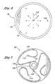
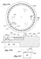
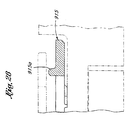
- An apparatus for processing a generally planar substrate (44) on a susceptor (42) having an area for receiving said substrate, with one or more spacers (100) extending above the susceptor to support the substrate and form a gap between the substrate and the susceptor, characterized by including:one or more passages (110) in said susceptor for introducing sweep gas from beneath said susceptor into said gap to flow radially outwardly from beneath the substrate; anda blocker ring (815) supported on said susceptor at the periphery of said area to be beneath an outer annular portion of the substrate, the ring being configured to restrict said outward radial flow of sweep gas and block gas above the susceptor from flowing into said area.
- The apparatus of Claim 1, wherein the ring is configured to create a thin annular sweep gas passage between the ring and the substrate.
- The apparatus of Claims 1 or 2, wherein said ring has an annular rib (815a) extending upwardly from a main body portion of the ring.
- The apparatus of Claim 3, wherein said rib is approximately centered between inner and outer diameters of the ring or is located adjacent an inner diameter of the ring.
- The apparatus of any of the preceding claims, wherein said ring has a plurality of circumferentially spaced legs (815c) which create a plurality of circumferentially spaced passages between the ring and the susceptor, whereby restricted sweep gas flow is permitted above and below the ring.
- The apparatus of any of the preceding claims, wherein said spacers are integral with said ring extending upwardly from a main body portion (815b) of the ring to create circumferentially spaced passages between the ring and the substrate.
- The apparatus of Claim 1, wherein said ring includes a plurality of circumferentially spaced legs depending from a main body portion of the ring, thereby creating a plurality of circumferentially spaced passages between the ring and the susceptor, and said spacers are circumferentially spaced from said legs so that a thermal path between the bottom surface of a leg and the top surface of an adjacent spacer is greater than the height of the ring including the spacer and the leg.
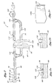
- The apparatus of any of claims 5, 6 or 7, wherein said susceptor includes a substantially disk-shaped lower section (80) and a substantially disk-shaped upper section (78), having a lower surface in engagement with an upper surface of said lower section, said one or more gas passages being defined by engaging surfaces of said sections, one or more gas inlets (142) in said lower section opening to its lower surface and said passages, and one or more gas outlets (96) in said upper section opening into said gap.
- The apparatus of Claim 8, wherein said one or more gas passages include a shallow annular (112) recess extending between said gas inlets and outlets.
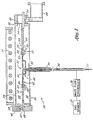
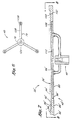
- The apparatus of Claim 8, including a support (32) for said susceptor, having a central shaft (36) and a plurality of support arms (74) extending radially and upwardly from said shaft, with the arms having upper ends adapted to engage the lower surface of said susceptor to support the susceptor, one or more of said arms being tubular so that said sweep gas may be conducted through said tubular arms into said gas inlets.
- The apparatus of any of the preceding claims, wherein said susceptor has a shallow recess (92) which forms said substrate receiving area, and said ring is slightly smaller than the inner diameter of the recess to fit within the recess between a substrate and the susceptor at the outer periphery of the substrate.
- A method of supporting a substrate during high temperature processing of the substrate, comprising:positioning the substrate spaced above a susceptor so that the substrate which is a wafer is substantially thermally decoupled from the susceptor; andpositioning a blocker ring on said susceptor beneath the outer periphery of said substrate said ring being configured to restrict an outward radial flow of sweep gas and block gas, introduced in one or more passages in said susceptor, from flowing into said area.
- The method of Claim 12, including supporting said substrate on said ring or on one or more spacers extending above the susceptor.
- The method of Claims 12 or 13, including:providing passages in said susceptor for introducing sweep gas into a gap between the substrate and the susceptor and to flow radially outwardly from beneath the substrate through one or more restricted passages past said blocker ring.
Priority Applications (1)
| Application Number | Priority Date | Filing Date | Title |
|---|---|---|---|
| EP01129575A EP1209251B1 (en) | 1997-01-23 | 1998-01-23 | Temperature control system for wafer |
Applications Claiming Priority (7)
| Application Number | Priority Date | Filing Date | Title |
|---|---|---|---|
| US788817 | 1985-10-18 | ||
| US78881797A | 1997-01-23 | 1997-01-23 | |
| US3985097P | 1997-03-05 | 1997-03-05 | |
| US39850P | 1997-03-05 | ||
| US923241 | 1997-09-04 | ||
| US08/923,241 US6113702A (en) | 1995-09-01 | 1997-09-04 | Wafer support system |
| PCT/US1998/001385 WO1998032893A2 (en) | 1997-01-23 | 1998-01-23 | Wafer support system |
Related Child Applications (1)
| Application Number | Title | Priority Date | Filing Date |
|---|---|---|---|
| EP01129575A Division EP1209251B1 (en) | 1997-01-23 | 1998-01-23 | Temperature control system for wafer |
Publications (2)
| Publication Number | Publication Date |
|---|---|
| EP0963459A2 EP0963459A2 (en) | 1999-12-15 |
| EP0963459B1 true EP0963459B1 (en) | 2002-07-17 |
Family
ID=27365616
Family Applications (2)
| Application Number | Title | Priority Date | Filing Date |
|---|---|---|---|
| EP01129575A Expired - Lifetime EP1209251B1 (en) | 1997-01-23 | 1998-01-23 | Temperature control system for wafer |
| EP98903702A Expired - Lifetime EP0963459B1 (en) | 1997-01-23 | 1998-01-23 | Wafer support apparatus |
Family Applications Before (1)
| Application Number | Title | Priority Date | Filing Date |
|---|---|---|---|
| EP01129575A Expired - Lifetime EP1209251B1 (en) | 1997-01-23 | 1998-01-23 | Temperature control system for wafer |
Country Status (7)
| Country | Link |
|---|---|
| US (7) | US6113702A (en) |
| EP (2) | EP1209251B1 (en) |
| JP (1) | JP4114016B2 (en) |
| KR (2) | KR100539343B1 (en) |
| AU (1) | AU6040498A (en) |
| DE (2) | DE69806578T2 (en) |
| WO (1) | WO1998032893A2 (en) |
Families Citing this family (482)
| Publication number | Priority date | Publication date | Assignee | Title |
|---|---|---|---|---|
| US6093252A (en) * | 1995-08-03 | 2000-07-25 | Asm America, Inc. | Process chamber with inner support |
| US6113702A (en) * | 1995-09-01 | 2000-09-05 | Asm America, Inc. | Wafer support system |
| US6046439A (en) * | 1996-06-17 | 2000-04-04 | Mattson Technology, Inc. | System and method for thermal processing of a semiconductor substrate |
| DE59610182D1 (en) * | 1996-11-01 | 2003-04-03 | Theva Duennschichttechnik Gmbh | DEVICE FOR PRODUCING OXIDIC THIN FILMS |
| US6200911B1 (en) * | 1998-04-21 | 2001-03-13 | Applied Materials, Inc. | Method and apparatus for modifying the profile of narrow, high-aspect-ratio gaps using differential plasma power |
| US6449428B2 (en) * | 1998-12-11 | 2002-09-10 | Mattson Technology Corp. | Gas driven rotating susceptor for rapid thermal processing (RTP) system |
| DE19901291C2 (en) * | 1999-01-15 | 2002-04-18 | Sez Semiconduct Equip Zubehoer | Device for the etching treatment of a disc-shaped object |
| US6524389B1 (en) * | 1999-05-24 | 2003-02-25 | Tokyo Electron Limited | Substrate processing apparatus |
| US6494955B1 (en) * | 2000-02-15 | 2002-12-17 | Applied Materials, Inc. | Ceramic substrate support |
| US20080156657A1 (en) * | 2000-02-17 | 2008-07-03 | Butterfield Paul D | Conductive polishing article for electrochemical mechanical polishing |
| US20040020789A1 (en) * | 2000-02-17 | 2004-02-05 | Applied Materials, Inc. | Conductive polishing article for electrochemical mechanical polishing |
| US7374644B2 (en) * | 2000-02-17 | 2008-05-20 | Applied Materials, Inc. | Conductive polishing article for electrochemical mechanical polishing |
| EP1174910A3 (en) * | 2000-07-20 | 2010-01-06 | Applied Materials, Inc. | Method and apparatus for dechucking a substrate |
| JP4526683B2 (en) * | 2000-10-31 | 2010-08-18 | 株式会社山形信越石英 | Quartz glass wafer support jig and manufacturing method thereof |
| JP2002158178A (en) * | 2000-11-21 | 2002-05-31 | Hitachi Kokusai Electric Inc | Substrate processing apparatus and method of manufacturing semiconductor device |
| SE0004296D0 (en) * | 2000-11-23 | 2000-11-23 | Gyros Ab | Device and method for the controlled heating in micro channel systems |
| US6634882B2 (en) * | 2000-12-22 | 2003-10-21 | Asm America, Inc. | Susceptor pocket profile to improve process performance |
| US6506252B2 (en) * | 2001-02-07 | 2003-01-14 | Emcore Corporation | Susceptorless reactor for growing epitaxial layers on wafers by chemical vapor deposition |
| US6600138B2 (en) * | 2001-04-17 | 2003-07-29 | Mattson Technology, Inc. | Rapid thermal processing system for integrated circuits |
| US6528767B2 (en) * | 2001-05-22 | 2003-03-04 | Applied Materials, Inc. | Pre-heating and load lock pedestal material for high temperature CVD liquid crystal and flat panel display applications |
| JP2004533118A (en) | 2001-05-30 | 2004-10-28 | エーエスエム アメリカ インコーポレイテッド | Low temperature loading and unloading and baking |
| US6919058B2 (en) * | 2001-08-28 | 2005-07-19 | Gyros Ab | Retaining microfluidic microcavity and other microfluidic structures |
| US20050000449A1 (en) * | 2001-12-21 | 2005-01-06 | Masayuki Ishibashi | Susceptor for epitaxial growth and epitaxial growth method |
| US7033445B2 (en) * | 2001-12-27 | 2006-04-25 | Asm America, Inc. | Gridded susceptor |
| US6730175B2 (en) * | 2002-01-22 | 2004-05-04 | Applied Materials, Inc. | Ceramic substrate support |
| US6677167B2 (en) * | 2002-03-04 | 2004-01-13 | Hitachi High-Technologies Corporation | Wafer processing apparatus and a wafer stage and a wafer processing method |
| US20030168174A1 (en) | 2002-03-08 | 2003-09-11 | Foree Michael Todd | Gas cushion susceptor system |
| DE10211312A1 (en) * | 2002-03-14 | 2003-10-02 | Wacker Siltronic Halbleitermat | Epitaxial coating applying method of semiconductor wafer in chemical vapor deposition reactor, involves exposing back surface of semiconductor wafer to ejection gas containing specific amount of hydrogen |
| US6861321B2 (en) * | 2002-04-05 | 2005-03-01 | Asm America, Inc. | Method of loading a wafer onto a wafer holder to reduce thermal shock |
| US7070660B2 (en) * | 2002-05-03 | 2006-07-04 | Asm America, Inc. | Wafer holder with stiffening rib |
| US6887317B2 (en) * | 2002-09-10 | 2005-05-03 | Applied Materials, Inc. | Reduced friction lift pin |
| DE10243022A1 (en) * | 2002-09-17 | 2004-03-25 | Degussa Ag | Separation of a solid by thermal decomposition of a gaseous substance in a cup reactor |
| US20040096636A1 (en) * | 2002-11-18 | 2004-05-20 | Applied Materials, Inc. | Lifting glass substrate without center lift pins |
| US20050170314A1 (en) * | 2002-11-27 | 2005-08-04 | Richard Golden | Dental pliers design with offsetting jaw and pad elements for assisting in removing upper and lower teeth and method for removing teeth utilizing the dental plier design |
| US6709267B1 (en) | 2002-12-27 | 2004-03-23 | Asm America, Inc. | Substrate holder with deep annular groove to prevent edge heat loss |
| US6917755B2 (en) * | 2003-02-27 | 2005-07-12 | Applied Materials, Inc. | Substrate support |
| US20040187787A1 (en) * | 2003-03-31 | 2004-09-30 | Dawson Keith E. | Substrate support having temperature controlled substrate support surface |
| US20040226513A1 (en) * | 2003-05-12 | 2004-11-18 | Applied Materials, Inc. | Chamber for uniform heating of large area substrates |
| DE10323085A1 (en) * | 2003-05-22 | 2004-12-09 | Aixtron Ag | CVD coater |
| JP4033809B2 (en) * | 2003-06-16 | 2008-01-16 | 東京エレクトロン株式会社 | Heat treatment apparatus and heat treatment method |
| EP1654752B1 (en) * | 2003-08-01 | 2011-06-29 | SGL Carbon SE | Holder for supporting wafers during semiconductor manufacture |
| JP4655935B2 (en) * | 2003-10-01 | 2011-03-23 | 信越半導体株式会社 | Manufacturing method of silicon epitaxial wafer |
| US7654221B2 (en) * | 2003-10-06 | 2010-02-02 | Applied Materials, Inc. | Apparatus for electroless deposition of metals onto semiconductor substrates |
| US7827930B2 (en) | 2004-01-26 | 2010-11-09 | Applied Materials, Inc. | Apparatus for electroless deposition of metals onto semiconductor substrates |
| US7311779B2 (en) * | 2003-10-06 | 2007-12-25 | Applied Materials, Inc. | Heating apparatus to heat wafers using water and plate with turbolators |
| US7323058B2 (en) | 2004-01-26 | 2008-01-29 | Applied Materials, Inc. | Apparatus for electroless deposition of metals onto semiconductor substrates |
| US7223308B2 (en) * | 2003-10-06 | 2007-05-29 | Applied Materials, Inc. | Apparatus to improve wafer temperature uniformity for face-up wet processing |
| JP4644676B2 (en) * | 2003-10-06 | 2011-03-02 | アプライド マテリアルズ インコーポレイテッド | Equipment to improve wafer temperature uniformity for face-up wet processing |
| US20050092439A1 (en) * | 2003-10-29 | 2005-05-05 | Keeton Tony J. | Low/high temperature substrate holder to reduce edge rolloff and backside damage |
| US7169234B2 (en) * | 2004-01-30 | 2007-01-30 | Asm America, Inc. | Apparatus and methods for preventing rotational slippage between a vertical shaft and a support structure for a semiconductor wafer holder |
| US20050176252A1 (en) * | 2004-02-10 | 2005-08-11 | Goodman Matthew G. | Two-stage load for processing both sides of a wafer |
| US8033245B2 (en) * | 2004-02-12 | 2011-10-11 | Applied Materials, Inc. | Substrate support bushing |
| KR101112029B1 (en) * | 2004-02-13 | 2012-03-21 | 에이에스엠 아메리카, 인코포레이티드 | Substrate Support System for Reduced Autodoping and Backside Deposition |
| US20070000527A1 (en) * | 2005-06-30 | 2007-01-04 | Aegerter Brian K | Workpiece support for use in a process vessel and system for treating microelectronic workpieces |
| EP1731966A4 (en) * | 2004-03-30 | 2008-01-16 | Pioneer Corp | Exposure equipment |
| US20060005770A1 (en) * | 2004-07-09 | 2006-01-12 | Robin Tiner | Independently moving substrate supports |
| US20060054090A1 (en) * | 2004-09-15 | 2006-03-16 | Applied Materials, Inc. | PECVD susceptor support construction |
| US7255747B2 (en) * | 2004-12-22 | 2007-08-14 | Sokudo Co., Ltd. | Coat/develop module with independent stations |
| US7126092B2 (en) * | 2005-01-13 | 2006-10-24 | Watlow Electric Manufacturing Company | Heater for wafer processing and methods of operating and manufacturing the same |
| WO2006078666A2 (en) | 2005-01-18 | 2006-07-27 | Asm America, Inc. | Reaction system for growing a thin film |
| CN101495668A (en) * | 2005-01-18 | 2009-07-29 | Asm美国公司 | Wafer support pin assembly |
| US7787411B2 (en) * | 2005-05-10 | 2010-08-31 | Microsoft Corporation | Gaming console wireless protocol for peripheral devices |
| US7262390B2 (en) * | 2005-05-23 | 2007-08-28 | Chung Shan Institute Of Science And Technology, Armaments Bureau, M.N.D. | Apparatus and adjusting technology for uniform thermal processing |
| US20070032081A1 (en) | 2005-08-08 | 2007-02-08 | Jeremy Chang | Edge ring assembly with dielectric spacer ring |
| US7418921B2 (en) * | 2005-08-12 | 2008-09-02 | Asm Japan K.K. | Plasma CVD apparatus for forming uniform film |
| US8628622B2 (en) * | 2005-09-12 | 2014-01-14 | Cree, Inc. | Gas driven rotation apparatus and method for forming crystalline layers |
| DE102005045338B4 (en) | 2005-09-22 | 2009-04-02 | Siltronic Ag | Epitaxial silicon wafer and process for producing epitaxially coated silicon wafers |
| TWI327761B (en) * | 2005-10-07 | 2010-07-21 | Rohm & Haas Elect Mat | Method for making semiconductor wafer and wafer holding article |
| US20070089836A1 (en) * | 2005-10-24 | 2007-04-26 | Applied Materials, Inc. | Semiconductor process chamber |
| KR101332206B1 (en) * | 2005-12-02 | 2013-11-25 | 롬 앤드 하스 일렉트로닉 머트어리얼즈, 엘.엘.씨. | Semiconductor processing |
| JP4629574B2 (en) | 2005-12-27 | 2011-02-09 | 日本発條株式会社 | Substrate support device and manufacturing method thereof |
| US7740518B2 (en) * | 2006-03-06 | 2010-06-22 | Michael Elliott | Jousting toy |
| US8278176B2 (en) * | 2006-06-07 | 2012-10-02 | Asm America, Inc. | Selective epitaxial formation of semiconductor films |
| US20080128088A1 (en) * | 2006-10-30 | 2008-06-05 | Jusung Engineering Co., Ltd. | Etching apparatus for edges of substrate |
| US7976634B2 (en) | 2006-11-21 | 2011-07-12 | Applied Materials, Inc. | Independent radiant gas preheating for precursor disassociation control and gas reaction kinetics in low temperature CVD systems |
| US8491752B2 (en) * | 2006-12-15 | 2013-07-23 | Tokyo Electron Limited | Substrate mounting table and method for manufacturing same, substrate processing apparatus, and fluid supply mechanism |
| KR100824301B1 (en) * | 2006-12-21 | 2008-04-22 | 세메스 주식회사 | Reaction chamber, and apparatus and system of collecting carbon nano tube having the same |
| US8057601B2 (en) * | 2007-05-09 | 2011-11-15 | Applied Materials, Inc. | Apparatus and method for supporting, positioning and rotating a substrate in a processing chamber |
| US8057602B2 (en) * | 2007-05-09 | 2011-11-15 | Applied Materials, Inc. | Apparatus and method for supporting, positioning and rotating a substrate in a processing chamber |
| US8034410B2 (en) * | 2007-07-17 | 2011-10-11 | Asm International N.V. | Protective inserts to line holes in parts for semiconductor process equipment |
| JP4971078B2 (en) * | 2007-08-30 | 2012-07-11 | 東京応化工業株式会社 | Surface treatment equipment |
| JP5169097B2 (en) * | 2007-09-14 | 2013-03-27 | 住友電気工業株式会社 | Semiconductor device manufacturing apparatus and manufacturing method |
| US7759199B2 (en) * | 2007-09-19 | 2010-07-20 | Asm America, Inc. | Stressor for engineered strain on channel |
| JP5260023B2 (en) * | 2007-10-19 | 2013-08-14 | 三菱重工業株式会社 | Plasma deposition system |
| US8067061B2 (en) * | 2007-10-25 | 2011-11-29 | Asm America, Inc. | Reaction apparatus having multiple adjustable exhaust ports |
| US8092606B2 (en) * | 2007-12-18 | 2012-01-10 | Asm Genitech Korea Ltd. | Deposition apparatus |
| US8107800B2 (en) * | 2008-01-08 | 2012-01-31 | International Business Machines Corporation | Method and structure to control thermal gradients in semiconductor wafers during rapid thermal processing |
| US20090181553A1 (en) | 2008-01-11 | 2009-07-16 | Blake Koelmel | Apparatus and method of aligning and positioning a cold substrate on a hot surface |
| US8198567B2 (en) | 2008-01-15 | 2012-06-12 | Applied Materials, Inc. | High temperature vacuum chuck assembly |
| US20090280248A1 (en) * | 2008-05-06 | 2009-11-12 | Asm America, Inc. | Porous substrate holder with thinned portions |
| US8053036B2 (en) * | 2008-06-02 | 2011-11-08 | Asm Japan K.K. | Method for designing shower plate for plasma CVD apparatus |
| US8394229B2 (en) * | 2008-08-07 | 2013-03-12 | Asm America, Inc. | Susceptor ring |
| US20100101491A1 (en) * | 2008-10-29 | 2010-04-29 | Asm Japan K.K. | Wafer lift pins suspended and supported at underside of susceptor |
| US20100107974A1 (en) * | 2008-11-06 | 2010-05-06 | Asm America, Inc. | Substrate holder with varying density |
| US8209833B2 (en) * | 2008-11-07 | 2012-07-03 | Tokyo Electron Limited | Thermal processing system and method of using |
| US10378106B2 (en) | 2008-11-14 | 2019-08-13 | Asm Ip Holding B.V. | Method of forming insulation film by modified PEALD |
| JP2010129709A (en) * | 2008-11-27 | 2010-06-10 | Kyocera Corp | Sample supporter, and heating device |
| US20100203242A1 (en) * | 2009-02-06 | 2010-08-12 | Applied Materials, Inc. | self-cleaning susceptor for solar cell processing |
| KR101680751B1 (en) | 2009-02-11 | 2016-12-12 | 어플라이드 머티어리얼스, 인코포레이티드 | Non-contact substrate processing |
| US9394608B2 (en) | 2009-04-06 | 2016-07-19 | Asm America, Inc. | Semiconductor processing reactor and components thereof |
| KR101681897B1 (en) * | 2009-08-07 | 2016-12-05 | 어플라이드 머티어리얼스, 인코포레이티드 | Dual temperature heater |
| US8802201B2 (en) | 2009-08-14 | 2014-08-12 | Asm America, Inc. | Systems and methods for thin-film deposition of metal oxides using excited nitrogen-oxygen species |
| US20110052159A1 (en) * | 2009-09-03 | 2011-03-03 | Chiung-Chieh Su | Apparatus for uniform thermal processing |
| US8367528B2 (en) * | 2009-11-17 | 2013-02-05 | Asm America, Inc. | Cyclical epitaxial deposition and etch |
| US20110127252A1 (en) * | 2009-11-27 | 2011-06-02 | Tangteck Equipment Inc. | Heating device having a function of dynamical temperature-control |
| SG183432A1 (en) | 2010-02-24 | 2012-09-27 | Veeco Instr Inc | Processing methods and apparatus with temperature distribution control |
| US9240513B2 (en) * | 2010-05-14 | 2016-01-19 | Solarcity Corporation | Dynamic support system for quartz process chamber |
| US9441295B2 (en) | 2010-05-14 | 2016-09-13 | Solarcity Corporation | Multi-channel gas-delivery system |
| US8591700B2 (en) * | 2010-08-19 | 2013-11-26 | Stmicroelectronics Pte Ltd. | Susceptor support system |
| JP5787526B2 (en) * | 2011-01-17 | 2015-09-30 | イビデン株式会社 | Electronic component positioning jig |
| JP5384549B2 (en) * | 2011-03-28 | 2014-01-08 | 株式会社小松製作所 | Heating device |
| DE102011007682A1 (en) * | 2011-04-19 | 2012-10-25 | Siltronic Ag | Susceptor for supporting a semiconductor wafer and method for depositing a layer on a front side of a semiconductor wafer |
| US8951350B2 (en) * | 2011-05-03 | 2015-02-10 | United Technologies Corporation | Coating methods and apparatus |
| DE112011105215A5 (en) * | 2011-05-06 | 2014-05-15 | Osram Opto Semiconductors Gmbh | A component carrier assembly with a trench structure separating a component carrier regions and a method for producing a plurality of component carrier regions |
| JP5712782B2 (en) * | 2011-05-13 | 2015-05-07 | 株式会社Sumco | Susceptor support shaft for epitaxial wafer growth apparatus and epitaxial growth apparatus |
| US8809170B2 (en) | 2011-05-19 | 2014-08-19 | Asm America Inc. | High throughput cyclical epitaxial deposition and etch process |
| US9312155B2 (en) | 2011-06-06 | 2016-04-12 | Asm Japan K.K. | High-throughput semiconductor-processing apparatus equipped with multiple dual-chamber modules |
| JP2013004593A (en) * | 2011-06-14 | 2013-01-07 | Sharp Corp | Substrate support apparatus and vapor deposition apparatus |
| US9793148B2 (en) | 2011-06-22 | 2017-10-17 | Asm Japan K.K. | Method for positioning wafers in multiple wafer transport |
| US10364496B2 (en) | 2011-06-27 | 2019-07-30 | Asm Ip Holding B.V. | Dual section module having shared and unshared mass flow controllers |
| US10854498B2 (en) | 2011-07-15 | 2020-12-01 | Asm Ip Holding B.V. | Wafer-supporting device and method for producing same |
| US20130023129A1 (en) | 2011-07-20 | 2013-01-24 | Asm America, Inc. | Pressure transmitter for a semiconductor processing environment |
| CN103035559B (en) * | 2011-09-29 | 2015-04-22 | 中芯国际集成电路制造(北京)有限公司 | Elastic fixed wheel and wafer adapter including the same |
| US9017481B1 (en) | 2011-10-28 | 2015-04-28 | Asm America, Inc. | Process feed management for semiconductor substrate processing |
| US9816184B2 (en) | 2012-03-20 | 2017-11-14 | Veeco Instruments Inc. | Keyed wafer carrier |
| DE102012205616B4 (en) * | 2012-04-04 | 2016-07-14 | Siltronic Ag | Device for depositing a layer on a semiconductor wafer by means of vapor deposition |
| US8946830B2 (en) | 2012-04-04 | 2015-02-03 | Asm Ip Holdings B.V. | Metal oxide protective layer for a semiconductor device |
| US9159597B2 (en) * | 2012-05-15 | 2015-10-13 | Taiwan Semiconductor Manufacturing Company, Ltd. | Real-time calibration for wafer processing chamber lamp modules |
| KR101482424B1 (en) * | 2012-07-24 | 2015-01-15 | 오씨아이 주식회사 | Silicon wafer recrystaliztion device and method of recrystalizing silicon wafer |
| US9558931B2 (en) | 2012-07-27 | 2017-01-31 | Asm Ip Holding B.V. | System and method for gas-phase sulfur passivation of a semiconductor surface |
| US9659799B2 (en) | 2012-08-28 | 2017-05-23 | Asm Ip Holding B.V. | Systems and methods for dynamic semiconductor process scheduling |
| US9021985B2 (en) | 2012-09-12 | 2015-05-05 | Asm Ip Holdings B.V. | Process gas management for an inductively-coupled plasma deposition reactor |
| US9324811B2 (en) | 2012-09-26 | 2016-04-26 | Asm Ip Holding B.V. | Structures and devices including a tensile-stressed silicon arsenic layer and methods of forming same |
| US10714315B2 (en) | 2012-10-12 | 2020-07-14 | Asm Ip Holdings B.V. | Semiconductor reaction chamber showerhead |
| US9589818B2 (en) * | 2012-12-20 | 2017-03-07 | Lam Research Ag | Apparatus for liquid treatment of wafer shaped articles and liquid control ring for use in same |
| US9640416B2 (en) | 2012-12-26 | 2017-05-02 | Asm Ip Holding B.V. | Single-and dual-chamber module-attachable wafer-handling chamber |
| JP6047854B2 (en) * | 2013-01-16 | 2016-12-21 | 信越半導体株式会社 | Single wafer epitaxial wafer manufacturing apparatus and epitaxial wafer manufacturing method using the same |
| US9543186B2 (en) * | 2013-02-01 | 2017-01-10 | Applied Materials, Inc. | Substrate support with controlled sealing gap |
| US20160376700A1 (en) | 2013-02-01 | 2016-12-29 | Asm Ip Holding B.V. | System for treatment of deposition reactor |
| US9589770B2 (en) | 2013-03-08 | 2017-03-07 | Asm Ip Holding B.V. | Method and systems for in-situ formation of intermediate reactive species |
| US9484191B2 (en) | 2013-03-08 | 2016-11-01 | Asm Ip Holding B.V. | Pulsed remote plasma method and system |
| US9273413B2 (en) | 2013-03-14 | 2016-03-01 | Veeco Instruments Inc. | Wafer carrier with temperature distribution control |
| US9991153B2 (en) * | 2013-03-14 | 2018-06-05 | Applied Materials, Inc. | Substrate support bushing |
| KR101586181B1 (en) * | 2013-03-28 | 2016-01-15 | 시바우라 메카트로닉스 가부시끼가이샤 | Carrying stand and plasma processing device |
| DE102013106461B4 (en) * | 2013-06-20 | 2016-10-27 | Kgt Graphit Technologie Gmbh | Holding pens for holding wafers in wafer boats and methods of making such pegs |
| US8993054B2 (en) | 2013-07-12 | 2015-03-31 | Asm Ip Holding B.V. | Method and system to reduce outgassing in a reaction chamber |
| US9018111B2 (en) | 2013-07-22 | 2015-04-28 | Asm Ip Holding B.V. | Semiconductor reaction chamber with plasma capabilities |
| DE102013012082A1 (en) * | 2013-07-22 | 2015-01-22 | Aixtron Se | Device for the thermal treatment of a semiconductor substrate, in particular for applying a coating |
| US9793115B2 (en) | 2013-08-14 | 2017-10-17 | Asm Ip Holding B.V. | Structures and devices including germanium-tin films and methods of forming same |
| US9240412B2 (en) | 2013-09-27 | 2016-01-19 | Asm Ip Holding B.V. | Semiconductor structure and device and methods of forming same using selective epitaxial process |
| KR102173114B1 (en) * | 2013-10-04 | 2020-11-03 | 엘지이노텍 주식회사 | Susceptor |
| US9556516B2 (en) | 2013-10-09 | 2017-01-31 | ASM IP Holding B.V | Method for forming Ti-containing film by PEALD using TDMAT or TDEAT |
| US10179947B2 (en) | 2013-11-26 | 2019-01-15 | Asm Ip Holding B.V. | Method for forming conformal nitrided, oxidized, or carbonized dielectric film by atomic layer deposition |
| US20150194326A1 (en) * | 2014-01-07 | 2015-07-09 | Applied Materials, Inc. | Pecvd ceramic heater with wide range of operating temperatures |
| US10032601B2 (en) * | 2014-02-21 | 2018-07-24 | Varian Semiconductor Equipment Associates, Inc. | Platen support structure |
| US10683571B2 (en) | 2014-02-25 | 2020-06-16 | Asm Ip Holding B.V. | Gas supply manifold and method of supplying gases to chamber using same |
| US10167557B2 (en) | 2014-03-18 | 2019-01-01 | Asm Ip Holding B.V. | Gas distribution system, reactor including the system, and methods of using the same |
| US9447498B2 (en) | 2014-03-18 | 2016-09-20 | Asm Ip Holding B.V. | Method for performing uniform processing in gas system-sharing multiple reaction chambers |
| US11015245B2 (en) | 2014-03-19 | 2021-05-25 | Asm Ip Holding B.V. | Gas-phase reactor and system having exhaust plenum and components thereof |
| US9404587B2 (en) | 2014-04-24 | 2016-08-02 | ASM IP Holding B.V | Lockout tagout for semiconductor vacuum valve |
| US10858737B2 (en) | 2014-07-28 | 2020-12-08 | Asm Ip Holding B.V. | Showerhead assembly and components thereof |
| US9543180B2 (en) | 2014-08-01 | 2017-01-10 | Asm Ip Holding B.V. | Apparatus and method for transporting wafers between wafer carrier and process tool under vacuum |
| US9890456B2 (en) | 2014-08-21 | 2018-02-13 | Asm Ip Holding B.V. | Method and system for in situ formation of gas-phase compounds |
| US9517539B2 (en) | 2014-08-28 | 2016-12-13 | Taiwan Semiconductor Manufacturing Company, Ltd. | Wafer susceptor with improved thermal characteristics |
| US9657845B2 (en) | 2014-10-07 | 2017-05-23 | Asm Ip Holding B.V. | Variable conductance gas distribution apparatus and method |
| US10941490B2 (en) | 2014-10-07 | 2021-03-09 | Asm Ip Holding B.V. | Multiple temperature range susceptor, assembly, reactor and system including the susceptor, and methods of using the same |
| KR102300403B1 (en) | 2014-11-19 | 2021-09-09 | 에이에스엠 아이피 홀딩 비.브이. | Method of depositing thin film |
| KR102263121B1 (en) | 2014-12-22 | 2021-06-09 | 에이에스엠 아이피 홀딩 비.브이. | Semiconductor device and manufacuring method thereof |
| CN107112267B (en) | 2015-01-12 | 2020-09-22 | 应用材料公司 | Support assembly for substrate backside color change control |
| US9478415B2 (en) | 2015-02-13 | 2016-10-25 | Asm Ip Holding B.V. | Method for forming film having low resistance and shallow junction depth |
| WO2016131190A1 (en) | 2015-02-17 | 2016-08-25 | Solarcity Corporation | Method and system for improving solar cell manufacturing yield |
| US10529542B2 (en) | 2015-03-11 | 2020-01-07 | Asm Ip Holdings B.V. | Cross-flow reactor and method |
| US10276355B2 (en) | 2015-03-12 | 2019-04-30 | Asm Ip Holding B.V. | Multi-zone reactor, system including the reactor, and method of using the same |
| US9972740B2 (en) | 2015-06-07 | 2018-05-15 | Tesla, Inc. | Chemical vapor deposition tool and process for fabrication of photovoltaic structures |
| US10458018B2 (en) | 2015-06-26 | 2019-10-29 | Asm Ip Holding B.V. | Structures including metal carbide material, devices including the structures, and methods of forming same |
| US10600673B2 (en) | 2015-07-07 | 2020-03-24 | Asm Ip Holding B.V. | Magnetic susceptor to baseplate seal |
| US10043661B2 (en) | 2015-07-13 | 2018-08-07 | Asm Ip Holding B.V. | Method for protecting layer by forming hydrocarbon-based extremely thin film |
| US9899291B2 (en) | 2015-07-13 | 2018-02-20 | Asm Ip Holding B.V. | Method for protecting layer by forming hydrocarbon-based extremely thin film |
| US10083836B2 (en) | 2015-07-24 | 2018-09-25 | Asm Ip Holding B.V. | Formation of boron-doped titanium metal films with high work function |
| US10087525B2 (en) | 2015-08-04 | 2018-10-02 | Asm Ip Holding B.V. | Variable gap hard stop design |
| US9647114B2 (en) | 2015-08-14 | 2017-05-09 | Asm Ip Holding B.V. | Methods of forming highly p-type doped germanium tin films and structures and devices including the films |
| DE102015113956B4 (en) | 2015-08-24 | 2024-03-07 | Meyer Burger (Germany) Gmbh | Substrate carrier |
| US9711345B2 (en) | 2015-08-25 | 2017-07-18 | Asm Ip Holding B.V. | Method for forming aluminum nitride-based film by PEALD |
| US9960072B2 (en) | 2015-09-29 | 2018-05-01 | Asm Ip Holding B.V. | Variable adjustment for precise matching of multiple chamber cavity housings |
| US9909214B2 (en) | 2015-10-15 | 2018-03-06 | Asm Ip Holding B.V. | Method for depositing dielectric film in trenches by PEALD |
| US10211308B2 (en) | 2015-10-21 | 2019-02-19 | Asm Ip Holding B.V. | NbMC layers |
| US10322384B2 (en) | 2015-11-09 | 2019-06-18 | Asm Ip Holding B.V. | Counter flow mixer for process chamber |
| US9455138B1 (en) | 2015-11-10 | 2016-09-27 | Asm Ip Holding B.V. | Method for forming dielectric film in trenches by PEALD using H-containing gas |
| US9905420B2 (en) | 2015-12-01 | 2018-02-27 | Asm Ip Holding B.V. | Methods of forming silicon germanium tin films and structures and devices including the films |
| US9607837B1 (en) | 2015-12-21 | 2017-03-28 | Asm Ip Holding B.V. | Method for forming silicon oxide cap layer for solid state diffusion process |
| US9735024B2 (en) | 2015-12-28 | 2017-08-15 | Asm Ip Holding B.V. | Method of atomic layer etching using functional group-containing fluorocarbon |
| US9627221B1 (en) | 2015-12-28 | 2017-04-18 | Asm Ip Holding B.V. | Continuous process incorporating atomic layer etching |
| US11139308B2 (en) | 2015-12-29 | 2021-10-05 | Asm Ip Holding B.V. | Atomic layer deposition of III-V compounds to form V-NAND devices |
| US10468251B2 (en) | 2016-02-19 | 2019-11-05 | Asm Ip Holding B.V. | Method for forming spacers using silicon nitride film for spacer-defined multiple patterning |
| US9754779B1 (en) | 2016-02-19 | 2017-09-05 | Asm Ip Holding B.V. | Method for forming silicon nitride film selectively on sidewalls or flat surfaces of trenches |
| US10529554B2 (en) | 2016-02-19 | 2020-01-07 | Asm Ip Holding B.V. | Method for forming silicon nitride film selectively on sidewalls or flat surfaces of trenches |
| US10501866B2 (en) | 2016-03-09 | 2019-12-10 | Asm Ip Holding B.V. | Gas distribution apparatus for improved film uniformity in an epitaxial system |
| US10343920B2 (en) | 2016-03-18 | 2019-07-09 | Asm Ip Holding B.V. | Aligned carbon nanotubes |
| US9892913B2 (en) | 2016-03-24 | 2018-02-13 | Asm Ip Holding B.V. | Radial and thickness control via biased multi-port injection settings |
| KR20180122023A (en) * | 2016-03-28 | 2018-11-09 | 어플라이드 머티어리얼스, 인코포레이티드 | The susceptor support |
| US10190213B2 (en) | 2016-04-21 | 2019-01-29 | Asm Ip Holding B.V. | Deposition of metal borides |
| US10865475B2 (en) | 2016-04-21 | 2020-12-15 | Asm Ip Holding B.V. | Deposition of metal borides and silicides |
| US10087522B2 (en) | 2016-04-21 | 2018-10-02 | Asm Ip Holding B.V. | Deposition of metal borides |
| US10032628B2 (en) | 2016-05-02 | 2018-07-24 | Asm Ip Holding B.V. | Source/drain performance through conformal solid state doping |
| US10367080B2 (en) | 2016-05-02 | 2019-07-30 | Asm Ip Holding B.V. | Method of forming a germanium oxynitride film |
| JP6635871B2 (en) * | 2016-05-11 | 2020-01-29 | 東京エレクトロン株式会社 | Film forming equipment |
| KR102592471B1 (en) | 2016-05-17 | 2023-10-20 | 에이에스엠 아이피 홀딩 비.브이. | Method of forming metal interconnection and method of fabricating semiconductor device using the same |
| US9748434B1 (en) | 2016-05-24 | 2017-08-29 | Tesla, Inc. | Systems, method and apparatus for curing conductive paste |
| US11453943B2 (en) | 2016-05-25 | 2022-09-27 | Asm Ip Holding B.V. | Method for forming carbon-containing silicon/metal oxide or nitride film by ALD using silicon precursor and hydrocarbon precursor |
| US10388509B2 (en) | 2016-06-28 | 2019-08-20 | Asm Ip Holding B.V. | Formation of epitaxial layers via dislocation filtering |
| US9859151B1 (en) | 2016-07-08 | 2018-01-02 | Asm Ip Holding B.V. | Selective film deposition method to form air gaps |
| US10612137B2 (en) | 2016-07-08 | 2020-04-07 | Asm Ip Holdings B.V. | Organic reactants for atomic layer deposition |
| US9793135B1 (en) | 2016-07-14 | 2017-10-17 | ASM IP Holding B.V | Method of cyclic dry etching using etchant film |
| US10714385B2 (en) | 2016-07-19 | 2020-07-14 | Asm Ip Holding B.V. | Selective deposition of tungsten |
| JP6736404B2 (en) * | 2016-07-26 | 2020-08-05 | 株式会社ディスコ | Grinding machine |
| KR102354490B1 (en) | 2016-07-27 | 2022-01-21 | 에이에스엠 아이피 홀딩 비.브이. | Method of processing a substrate |
| US9887082B1 (en) | 2016-07-28 | 2018-02-06 | Asm Ip Holding B.V. | Method and apparatus for filling a gap |
| KR102532607B1 (en) | 2016-07-28 | 2023-05-15 | 에이에스엠 아이피 홀딩 비.브이. | Substrate processing apparatus and method of operating the same |
| US9812320B1 (en) | 2016-07-28 | 2017-11-07 | Asm Ip Holding B.V. | Method and apparatus for filling a gap |
| US10177025B2 (en) | 2016-07-28 | 2019-01-08 | Asm Ip Holding B.V. | Method and apparatus for filling a gap |
| US10395919B2 (en) | 2016-07-28 | 2019-08-27 | Asm Ip Holding B.V. | Method and apparatus for filling a gap |
| US9954136B2 (en) | 2016-08-03 | 2018-04-24 | Tesla, Inc. | Cassette optimized for an inline annealing system |
| US10090316B2 (en) | 2016-09-01 | 2018-10-02 | Asm Ip Holding B.V. | 3D stacked multilayer semiconductor memory using doped select transistor channel |
| US10410943B2 (en) | 2016-10-13 | 2019-09-10 | Asm Ip Holding B.V. | Method for passivating a surface of a semiconductor and related systems |
| JP6740084B2 (en) * | 2016-10-25 | 2020-08-12 | 株式会社ニューフレアテクノロジー | Vapor growth apparatus, annular holder, and vapor growth method |
| US10643826B2 (en) | 2016-10-26 | 2020-05-05 | Asm Ip Holdings B.V. | Methods for thermally calibrating reaction chambers |
| US11532757B2 (en) | 2016-10-27 | 2022-12-20 | Asm Ip Holding B.V. | Deposition of charge trapping layers |
| US10115856B2 (en) | 2016-10-31 | 2018-10-30 | Tesla, Inc. | System and method for curing conductive paste using induction heating |
| US10714350B2 (en) | 2016-11-01 | 2020-07-14 | ASM IP Holdings, B.V. | Methods for forming a transition metal niobium nitride film on a substrate by atomic layer deposition and related semiconductor device structures |
| US10435790B2 (en) | 2016-11-01 | 2019-10-08 | Asm Ip Holding B.V. | Method of subatmospheric plasma-enhanced ALD using capacitively coupled electrodes with narrow gap |
| US10643904B2 (en) | 2016-11-01 | 2020-05-05 | Asm Ip Holdings B.V. | Methods for forming a semiconductor device and related semiconductor device structures |
| US10229833B2 (en) | 2016-11-01 | 2019-03-12 | Asm Ip Holding B.V. | Methods for forming a transition metal nitride film on a substrate by atomic layer deposition and related semiconductor device structures |
| US10134757B2 (en) | 2016-11-07 | 2018-11-20 | Asm Ip Holding B.V. | Method of processing a substrate and a device manufactured by using the method |
| KR102546317B1 (en) | 2016-11-15 | 2023-06-21 | 에이에스엠 아이피 홀딩 비.브이. | Gas supply unit and substrate processing apparatus including the same |
| US10340135B2 (en) | 2016-11-28 | 2019-07-02 | Asm Ip Holding B.V. | Method of topologically restricted plasma-enhanced cyclic deposition of silicon or metal nitride |
| KR20180068582A (en) | 2016-12-14 | 2018-06-22 | 에이에스엠 아이피 홀딩 비.브이. | Substrate processing apparatus |
| US11447861B2 (en) | 2016-12-15 | 2022-09-20 | Asm Ip Holding B.V. | Sequential infiltration synthesis apparatus and a method of forming a patterned structure |
| US9916980B1 (en) | 2016-12-15 | 2018-03-13 | Asm Ip Holding B.V. | Method of forming a structure on a substrate |
| US11581186B2 (en) | 2016-12-15 | 2023-02-14 | Asm Ip Holding B.V. | Sequential infiltration synthesis apparatus |
| KR20180070971A (en) | 2016-12-19 | 2018-06-27 | 에이에스엠 아이피 홀딩 비.브이. | Substrate processing apparatus |
| US10269558B2 (en) | 2016-12-22 | 2019-04-23 | Asm Ip Holding B.V. | Method of forming a structure on a substrate |
| US10867788B2 (en) | 2016-12-28 | 2020-12-15 | Asm Ip Holding B.V. | Method of forming a structure on a substrate |
| US11390950B2 (en) | 2017-01-10 | 2022-07-19 | Asm Ip Holding B.V. | Reactor system and method to reduce residue buildup during a film deposition process |
| US10655221B2 (en) | 2017-02-09 | 2020-05-19 | Asm Ip Holding B.V. | Method for depositing oxide film by thermal ALD and PEALD |
| US10468261B2 (en) | 2017-02-15 | 2019-11-05 | Asm Ip Holding B.V. | Methods for forming a metallic film on a substrate by cyclical deposition and related semiconductor device structures |
| US11702748B2 (en) * | 2017-03-03 | 2023-07-18 | Lam Research Corporation | Wafer level uniformity control in remote plasma film deposition |
| US10529563B2 (en) | 2017-03-29 | 2020-01-07 | Asm Ip Holdings B.V. | Method for forming doped metal oxide films on a substrate by cyclical deposition and related semiconductor device structures |
| US10283353B2 (en) | 2017-03-29 | 2019-05-07 | Asm Ip Holding B.V. | Method of reforming insulating film deposited on substrate with recess pattern |
| US10103040B1 (en) | 2017-03-31 | 2018-10-16 | Asm Ip Holding B.V. | Apparatus and method for manufacturing a semiconductor device |
| US10829866B2 (en) * | 2017-04-03 | 2020-11-10 | Infineon Technologies Americas Corp. | Wafer carrier and method |
| USD830981S1 (en) | 2017-04-07 | 2018-10-16 | Asm Ip Holding B.V. | Susceptor for semiconductor substrate processing apparatus |
| KR102457289B1 (en) | 2017-04-25 | 2022-10-21 | 에이에스엠 아이피 홀딩 비.브이. | Method for depositing a thin film and manufacturing a semiconductor device |
| US10446393B2 (en) | 2017-05-08 | 2019-10-15 | Asm Ip Holding B.V. | Methods for forming silicon-containing epitaxial layers and related semiconductor device structures |
| US10892156B2 (en) | 2017-05-08 | 2021-01-12 | Asm Ip Holding B.V. | Methods for forming a silicon nitride film on a substrate and related semiconductor device structures |
| US10770286B2 (en) | 2017-05-08 | 2020-09-08 | Asm Ip Holdings B.V. | Methods for selectively forming a silicon nitride film on a substrate and related semiconductor device structures |
| US10504742B2 (en) | 2017-05-31 | 2019-12-10 | Asm Ip Holding B.V. | Method of atomic layer etching using hydrogen plasma |
| US10886123B2 (en) | 2017-06-02 | 2021-01-05 | Asm Ip Holding B.V. | Methods for forming low temperature semiconductor layers and related semiconductor device structures |
| US11306395B2 (en) | 2017-06-28 | 2022-04-19 | Asm Ip Holding B.V. | Methods for depositing a transition metal nitride film on a substrate by atomic layer deposition and related deposition apparatus |
| JP6809991B2 (en) * | 2017-06-30 | 2021-01-06 | 京セラ株式会社 | Spectrometer |
| US10685834B2 (en) | 2017-07-05 | 2020-06-16 | Asm Ip Holdings B.V. | Methods for forming a silicon germanium tin layer and related semiconductor device structures |
| KR20190009245A (en) | 2017-07-18 | 2019-01-28 | 에이에스엠 아이피 홀딩 비.브이. | Methods for forming a semiconductor device structure and related semiconductor device structures |
| US11374112B2 (en) | 2017-07-19 | 2022-06-28 | Asm Ip Holding B.V. | Method for depositing a group IV semiconductor and related semiconductor device structures |
| US10541333B2 (en) | 2017-07-19 | 2020-01-21 | Asm Ip Holding B.V. | Method for depositing a group IV semiconductor and related semiconductor device structures |
| US11018002B2 (en) | 2017-07-19 | 2021-05-25 | Asm Ip Holding B.V. | Method for selectively depositing a Group IV semiconductor and related semiconductor device structures |
| US10605530B2 (en) | 2017-07-26 | 2020-03-31 | Asm Ip Holding B.V. | Assembly of a liner and a flange for a vertical furnace as well as the liner and the vertical furnace |
| US10312055B2 (en) | 2017-07-26 | 2019-06-04 | Asm Ip Holding B.V. | Method of depositing film by PEALD using negative bias |
| US10590535B2 (en) | 2017-07-26 | 2020-03-17 | Asm Ip Holdings B.V. | Chemical treatment, deposition and/or infiltration apparatus and method for using the same |
| US10692741B2 (en) | 2017-08-08 | 2020-06-23 | Asm Ip Holdings B.V. | Radiation shield |
| US10770336B2 (en) | 2017-08-08 | 2020-09-08 | Asm Ip Holding B.V. | Substrate lift mechanism and reactor including same |
| US10249524B2 (en) | 2017-08-09 | 2019-04-02 | Asm Ip Holding B.V. | Cassette holder assembly for a substrate cassette and holding member for use in such assembly |
| US11139191B2 (en) | 2017-08-09 | 2021-10-05 | Asm Ip Holding B.V. | Storage apparatus for storing cassettes for substrates and processing apparatus equipped therewith |
| US11769682B2 (en) | 2017-08-09 | 2023-09-26 | Asm Ip Holding B.V. | Storage apparatus for storing cassettes for substrates and processing apparatus equipped therewith |
| US10236177B1 (en) | 2017-08-22 | 2019-03-19 | ASM IP Holding B.V.. | Methods for depositing a doped germanium tin semiconductor and related semiconductor device structures |
| USD900036S1 (en) | 2017-08-24 | 2020-10-27 | Asm Ip Holding B.V. | Heater electrical connector and adapter |
| US11830730B2 (en) | 2017-08-29 | 2023-11-28 | Asm Ip Holding B.V. | Layer forming method and apparatus |
| KR102491945B1 (en) | 2017-08-30 | 2023-01-26 | 에이에스엠 아이피 홀딩 비.브이. | Substrate processing apparatus |
| US11295980B2 (en) | 2017-08-30 | 2022-04-05 | Asm Ip Holding B.V. | Methods for depositing a molybdenum metal film over a dielectric surface of a substrate by a cyclical deposition process and related semiconductor device structures |
| US11056344B2 (en) | 2017-08-30 | 2021-07-06 | Asm Ip Holding B.V. | Layer forming method |
| US10607895B2 (en) | 2017-09-18 | 2020-03-31 | Asm Ip Holdings B.V. | Method for forming a semiconductor device structure comprising a gate fill metal |
| KR102630301B1 (en) | 2017-09-21 | 2024-01-29 | 에이에스엠 아이피 홀딩 비.브이. | Method of sequential infiltration synthesis treatment of infiltrateable material and structures and devices formed using same |
| US10844484B2 (en) | 2017-09-22 | 2020-11-24 | Asm Ip Holding B.V. | Apparatus for dispensing a vapor phase reactant to a reaction chamber and related methods |
| US10658205B2 (en) | 2017-09-28 | 2020-05-19 | Asm Ip Holdings B.V. | Chemical dispensing apparatus and methods for dispensing a chemical to a reaction chamber |
| US10403504B2 (en) | 2017-10-05 | 2019-09-03 | Asm Ip Holding B.V. | Method for selectively depositing a metallic film on a substrate |
| US10319588B2 (en) | 2017-10-10 | 2019-06-11 | Asm Ip Holding B.V. | Method for depositing a metal chalcogenide on a substrate by cyclical deposition |
| US10923344B2 (en) | 2017-10-30 | 2021-02-16 | Asm Ip Holding B.V. | Methods for forming a semiconductor structure and related semiconductor structures |
| US10872804B2 (en) | 2017-11-03 | 2020-12-22 | Asm Ip Holding B.V. | Apparatus and methods for isolating a reaction chamber from a loading chamber resulting in reduced contamination |
| US10872803B2 (en) | 2017-11-03 | 2020-12-22 | Asm Ip Holding B.V. | Apparatus and methods for isolating a reaction chamber from a loading chamber resulting in reduced contamination |
| KR102443047B1 (en) | 2017-11-16 | 2022-09-14 | 에이에스엠 아이피 홀딩 비.브이. | Method of processing a substrate and a device manufactured by the same |
| US10910262B2 (en) | 2017-11-16 | 2021-02-02 | Asm Ip Holding B.V. | Method of selectively depositing a capping layer structure on a semiconductor device structure |
| US11022879B2 (en) | 2017-11-24 | 2021-06-01 | Asm Ip Holding B.V. | Method of forming an enhanced unexposed photoresist layer |
| JP7214724B2 (en) | 2017-11-27 | 2023-01-30 | エーエスエム アイピー ホールディング ビー.ブイ. | Storage device for storing wafer cassettes used in batch furnaces |
| TWI791689B (en) | 2017-11-27 | 2023-02-11 | 荷蘭商Asm智慧財產控股私人有限公司 | Apparatus including a clean mini environment |
| US10290508B1 (en) | 2017-12-05 | 2019-05-14 | Asm Ip Holding B.V. | Method for forming vertical spacers for spacer-defined patterning |
| US10872771B2 (en) | 2018-01-16 | 2020-12-22 | Asm Ip Holding B. V. | Method for depositing a material film on a substrate within a reaction chamber by a cyclical deposition process and related device structures |
| CN111630203A (en) | 2018-01-19 | 2020-09-04 | Asm Ip私人控股有限公司 | Method for depositing gap filling layer by plasma auxiliary deposition |
| TW202325889A (en) | 2018-01-19 | 2023-07-01 | 荷蘭商Asm 智慧財產控股公司 | Deposition method |
| USD903477S1 (en) | 2018-01-24 | 2020-12-01 | Asm Ip Holdings B.V. | Metal clamp |
| US11018047B2 (en) | 2018-01-25 | 2021-05-25 | Asm Ip Holding B.V. | Hybrid lift pin |
| US10535516B2 (en) | 2018-02-01 | 2020-01-14 | Asm Ip Holdings B.V. | Method for depositing a semiconductor structure on a surface of a substrate and related semiconductor structures |
| USD880437S1 (en) | 2018-02-01 | 2020-04-07 | Asm Ip Holding B.V. | Gas supply plate for semiconductor manufacturing apparatus |
| US11081345B2 (en) | 2018-02-06 | 2021-08-03 | Asm Ip Holding B.V. | Method of post-deposition treatment for silicon oxide film |
| US10896820B2 (en) | 2018-02-14 | 2021-01-19 | Asm Ip Holding B.V. | Method for depositing a ruthenium-containing film on a substrate by a cyclical deposition process |
| JP7124098B2 (en) | 2018-02-14 | 2022-08-23 | エーエスエム・アイピー・ホールディング・ベー・フェー | Method for depositing a ruthenium-containing film on a substrate by a cyclical deposition process |
| US10731249B2 (en) | 2018-02-15 | 2020-08-04 | Asm Ip Holding B.V. | Method of forming a transition metal containing film on a substrate by a cyclical deposition process, a method for supplying a transition metal halide compound to a reaction chamber, and related vapor deposition apparatus |
| KR102636427B1 (en) | 2018-02-20 | 2024-02-13 | 에이에스엠 아이피 홀딩 비.브이. | Substrate processing method and apparatus |
| US10658181B2 (en) | 2018-02-20 | 2020-05-19 | Asm Ip Holding B.V. | Method of spacer-defined direct patterning in semiconductor fabrication |
| US10975470B2 (en) | 2018-02-23 | 2021-04-13 | Asm Ip Holding B.V. | Apparatus for detecting or monitoring for a chemical precursor in a high temperature environment |
| US11473195B2 (en) | 2018-03-01 | 2022-10-18 | Asm Ip Holding B.V. | Semiconductor processing apparatus and a method for processing a substrate |
| US11629406B2 (en) | 2018-03-09 | 2023-04-18 | Asm Ip Holding B.V. | Semiconductor processing apparatus comprising one or more pyrometers for measuring a temperature of a substrate during transfer of the substrate |
| US11114283B2 (en) | 2018-03-16 | 2021-09-07 | Asm Ip Holding B.V. | Reactor, system including the reactor, and methods of manufacturing and using same |
| KR102646467B1 (en) | 2018-03-27 | 2024-03-11 | 에이에스엠 아이피 홀딩 비.브이. | Method of forming an electrode on a substrate and a semiconductor device structure including an electrode |
| US11230766B2 (en) | 2018-03-29 | 2022-01-25 | Asm Ip Holding B.V. | Substrate processing apparatus and method |
| US10510536B2 (en) | 2018-03-29 | 2019-12-17 | Asm Ip Holding B.V. | Method of depositing a co-doped polysilicon film on a surface of a substrate within a reaction chamber |
| US11088002B2 (en) | 2018-03-29 | 2021-08-10 | Asm Ip Holding B.V. | Substrate rack and a substrate processing system and method |
| KR102501472B1 (en) | 2018-03-30 | 2023-02-20 | 에이에스엠 아이피 홀딩 비.브이. | Substrate processing method |
| KR20190128558A (en) | 2018-05-08 | 2019-11-18 | 에이에스엠 아이피 홀딩 비.브이. | Methods for depositing an oxide film on a substrate by a cyclical deposition process and related device structures |
| TW202349473A (en) | 2018-05-11 | 2023-12-16 | 荷蘭商Asm Ip私人控股有限公司 | Methods for forming a doped metal carbide film on a substrate and related semiconductor device structures |
| KR102596988B1 (en) | 2018-05-28 | 2023-10-31 | 에이에스엠 아이피 홀딩 비.브이. | Method of processing a substrate and a device manufactured by the same |
| US11718913B2 (en) | 2018-06-04 | 2023-08-08 | Asm Ip Holding B.V. | Gas distribution system and reactor system including same |
| US11270899B2 (en) | 2018-06-04 | 2022-03-08 | Asm Ip Holding B.V. | Wafer handling chamber with moisture reduction |
| US11286562B2 (en) | 2018-06-08 | 2022-03-29 | Asm Ip Holding B.V. | Gas-phase chemical reactor and method of using same |
| KR102568797B1 (en) | 2018-06-21 | 2023-08-21 | 에이에스엠 아이피 홀딩 비.브이. | Substrate processing system |
| US10797133B2 (en) | 2018-06-21 | 2020-10-06 | Asm Ip Holding B.V. | Method for depositing a phosphorus doped silicon arsenide film and related semiconductor device structures |
| CN112292478A (en) | 2018-06-27 | 2021-01-29 | Asm Ip私人控股有限公司 | Cyclic deposition methods for forming metal-containing materials and films and structures containing metal-containing materials |
| WO2020003000A1 (en) | 2018-06-27 | 2020-01-02 | Asm Ip Holding B.V. | Cyclic deposition methods for forming metal-containing material and films and structures including the metal-containing material |
| US10612136B2 (en) | 2018-06-29 | 2020-04-07 | ASM IP Holding, B.V. | Temperature-controlled flange and reactor system including same |
| KR20200002519A (en) | 2018-06-29 | 2020-01-08 | 에이에스엠 아이피 홀딩 비.브이. | Method for depositing a thin film and manufacturing a semiconductor device |
| US10755922B2 (en) | 2018-07-03 | 2020-08-25 | Asm Ip Holding B.V. | Method for depositing silicon-free carbon-containing film as gap-fill layer by pulse plasma-assisted deposition |
| US10388513B1 (en) | 2018-07-03 | 2019-08-20 | Asm Ip Holding B.V. | Method for depositing silicon-free carbon-containing film as gap-fill layer by pulse plasma-assisted deposition |
| US10767789B2 (en) | 2018-07-16 | 2020-09-08 | Asm Ip Holding B.V. | Diaphragm valves, valve components, and methods for forming valve components |
| US10483099B1 (en) | 2018-07-26 | 2019-11-19 | Asm Ip Holding B.V. | Method for forming thermally stable organosilicon polymer film |
| US11053591B2 (en) | 2018-08-06 | 2021-07-06 | Asm Ip Holding B.V. | Multi-port gas injection system and reactor system including same |
| US10883175B2 (en) | 2018-08-09 | 2021-01-05 | Asm Ip Holding B.V. | Vertical furnace for processing substrates and a liner for use therein |
| US10829852B2 (en) | 2018-08-16 | 2020-11-10 | Asm Ip Holding B.V. | Gas distribution device for a wafer processing apparatus |
| US11430674B2 (en) | 2018-08-22 | 2022-08-30 | Asm Ip Holding B.V. | Sensor array, apparatus for dispensing a vapor phase reactant to a reaction chamber and related methods |
| US11024523B2 (en) | 2018-09-11 | 2021-06-01 | Asm Ip Holding B.V. | Substrate processing apparatus and method |
| KR20200030162A (en) | 2018-09-11 | 2020-03-20 | 에이에스엠 아이피 홀딩 비.브이. | Method for deposition of a thin film |
| US11049751B2 (en) | 2018-09-14 | 2021-06-29 | Asm Ip Holding B.V. | Cassette supply system to store and handle cassettes and processing apparatus equipped therewith |
| CN110970344A (en) | 2018-10-01 | 2020-04-07 | Asm Ip控股有限公司 | Substrate holding apparatus, system including the same, and method of using the same |
| US11232963B2 (en) | 2018-10-03 | 2022-01-25 | Asm Ip Holding B.V. | Substrate processing apparatus and method |
| KR102592699B1 (en) | 2018-10-08 | 2023-10-23 | 에이에스엠 아이피 홀딩 비.브이. | Substrate support unit and apparatuses for depositing thin film and processing the substrate including the same |
| US10847365B2 (en) | 2018-10-11 | 2020-11-24 | Asm Ip Holding B.V. | Method of forming conformal silicon carbide film by cyclic CVD |
| US10811256B2 (en) | 2018-10-16 | 2020-10-20 | Asm Ip Holding B.V. | Method for etching a carbon-containing feature |
| KR102605121B1 (en) | 2018-10-19 | 2023-11-23 | 에이에스엠 아이피 홀딩 비.브이. | Substrate processing apparatus and substrate processing method |
| KR102546322B1 (en) | 2018-10-19 | 2023-06-21 | 에이에스엠 아이피 홀딩 비.브이. | Substrate processing apparatus and substrate processing method |
| USD948463S1 (en) | 2018-10-24 | 2022-04-12 | Asm Ip Holding B.V. | Susceptor for semiconductor substrate supporting apparatus |
| US10381219B1 (en) | 2018-10-25 | 2019-08-13 | Asm Ip Holding B.V. | Methods for forming a silicon nitride film |
| US11087997B2 (en) | 2018-10-31 | 2021-08-10 | Asm Ip Holding B.V. | Substrate processing apparatus for processing substrates |
| KR20200051105A (en) | 2018-11-02 | 2020-05-13 | 에이에스엠 아이피 홀딩 비.브이. | Substrate support unit and substrate processing apparatus including the same |
| US11572620B2 (en) | 2018-11-06 | 2023-02-07 | Asm Ip Holding B.V. | Methods for selectively depositing an amorphous silicon film on a substrate |
| US11031242B2 (en) | 2018-11-07 | 2021-06-08 | Asm Ip Holding B.V. | Methods for depositing a boron doped silicon germanium film |
| US10818758B2 (en) | 2018-11-16 | 2020-10-27 | Asm Ip Holding B.V. | Methods for forming a metal silicate film on a substrate in a reaction chamber and related semiconductor device structures |
| US10847366B2 (en) | 2018-11-16 | 2020-11-24 | Asm Ip Holding B.V. | Methods for depositing a transition metal chalcogenide film on a substrate by a cyclical deposition process |
| US10559458B1 (en) | 2018-11-26 | 2020-02-11 | Asm Ip Holding B.V. | Method of forming oxynitride film |
| US11217444B2 (en) | 2018-11-30 | 2022-01-04 | Asm Ip Holding B.V. | Method for forming an ultraviolet radiation responsive metal oxide-containing film |
| KR102636428B1 (en) | 2018-12-04 | 2024-02-13 | 에이에스엠 아이피 홀딩 비.브이. | A method for cleaning a substrate processing apparatus |
| JP7023826B2 (en) * | 2018-12-07 | 2022-02-22 | 株式会社ニューフレアテクノロジー | Continuous film formation method, continuous film formation equipment, susceptor unit, and spacer set used for susceptor unit. |
| DE102018131987A1 (en) * | 2018-12-12 | 2020-06-18 | Aixtron Se | Substrate holder for use in a CVD reactor |
| US11158513B2 (en) | 2018-12-13 | 2021-10-26 | Asm Ip Holding B.V. | Methods for forming a rhenium-containing film on a substrate by a cyclical deposition process and related semiconductor device structures |
| JP2020096183A (en) | 2018-12-14 | 2020-06-18 | エーエスエム・アイピー・ホールディング・ベー・フェー | Method of forming device structure using selective deposition of gallium nitride, and system for the same |
| USD914620S1 (en) | 2019-01-17 | 2021-03-30 | Asm Ip Holding B.V. | Vented susceptor |
| US11961756B2 (en) | 2019-01-17 | 2024-04-16 | Asm Ip Holding B.V. | Vented susceptor |
| TWI819180B (en) | 2019-01-17 | 2023-10-21 | 荷蘭商Asm 智慧財產控股公司 | Methods of forming a transition metal containing film on a substrate by a cyclical deposition process |
| USD920936S1 (en) | 2019-01-17 | 2021-06-01 | Asm Ip Holding B.V. | Higher temperature vented susceptor |
| KR20200091543A (en) | 2019-01-22 | 2020-07-31 | 에이에스엠 아이피 홀딩 비.브이. | Semiconductor processing device |
| CN111524788B (en) | 2019-02-01 | 2023-11-24 | Asm Ip私人控股有限公司 | Method for topologically selective film formation of silicon oxide |
| KR20200102357A (en) | 2019-02-20 | 2020-08-31 | 에이에스엠 아이피 홀딩 비.브이. | Apparatus and methods for plug fill deposition in 3-d nand applications |
| KR102626263B1 (en) | 2019-02-20 | 2024-01-16 | 에이에스엠 아이피 홀딩 비.브이. | Cyclical deposition method including treatment step and apparatus for same |
| TW202044325A (en) | 2019-02-20 | 2020-12-01 | 荷蘭商Asm Ip私人控股有限公司 | Method of filling a recess formed within a surface of a substrate, semiconductor structure formed according to the method, and semiconductor processing apparatus |
| TW202104632A (en) | 2019-02-20 | 2021-02-01 | 荷蘭商Asm Ip私人控股有限公司 | Cyclical deposition method and apparatus for filling a recess formed within a substrate surface |
| TW202100794A (en) | 2019-02-22 | 2021-01-01 | 荷蘭商Asm Ip私人控股有限公司 | Substrate processing apparatus and method for processing substrate |
| KR20200108242A (en) | 2019-03-08 | 2020-09-17 | 에이에스엠 아이피 홀딩 비.브이. | Method for Selective Deposition of Silicon Nitride Layer and Structure Including Selectively-Deposited Silicon Nitride Layer |
| US11742198B2 (en) | 2019-03-08 | 2023-08-29 | Asm Ip Holding B.V. | Structure including SiOCN layer and method of forming same |
| KR20200108243A (en) | 2019-03-08 | 2020-09-17 | 에이에스엠 아이피 홀딩 비.브이. | Structure Including SiOC Layer and Method of Forming Same |
| KR20200116033A (en) | 2019-03-28 | 2020-10-08 | 에이에스엠 아이피 홀딩 비.브이. | Door opener and substrate processing apparatus provided therewith |
| KR20200116855A (en) | 2019-04-01 | 2020-10-13 | 에이에스엠 아이피 홀딩 비.브이. | Method of manufacturing semiconductor device |
| KR20200123380A (en) | 2019-04-19 | 2020-10-29 | 에이에스엠 아이피 홀딩 비.브이. | Layer forming method and apparatus |
| KR20200125453A (en) | 2019-04-24 | 2020-11-04 | 에이에스엠 아이피 홀딩 비.브이. | Gas-phase reactor system and method of using same |
| KR20200130118A (en) | 2019-05-07 | 2020-11-18 | 에이에스엠 아이피 홀딩 비.브이. | Method for Reforming Amorphous Carbon Polymer Film |
| KR20200130121A (en) | 2019-05-07 | 2020-11-18 | 에이에스엠 아이피 홀딩 비.브이. | Chemical source vessel with dip tube |
| KR20200130652A (en) | 2019-05-10 | 2020-11-19 | 에이에스엠 아이피 홀딩 비.브이. | Method of depositing material onto a surface and structure formed according to the method |
| JP2020188255A (en) | 2019-05-16 | 2020-11-19 | エーエスエム アイピー ホールディング ビー.ブイ. | Wafer boat handling device, vertical batch furnace, and method |
| USD947913S1 (en) | 2019-05-17 | 2022-04-05 | Asm Ip Holding B.V. | Susceptor shaft |
| USD975665S1 (en) | 2019-05-17 | 2023-01-17 | Asm Ip Holding B.V. | Susceptor shaft |
| US11404302B2 (en) | 2019-05-22 | 2022-08-02 | Asm Ip Holding B.V. | Substrate susceptor using edge purging |
| USD935572S1 (en) | 2019-05-24 | 2021-11-09 | Asm Ip Holding B.V. | Gas channel plate |
| US11415463B2 (en) * | 2019-06-04 | 2022-08-16 | Applied Materials, Inc. | Contactless workpiece temperature sensor |
| USD922229S1 (en) | 2019-06-05 | 2021-06-15 | Asm Ip Holding B.V. | Device for controlling a temperature of a gas supply unit |
| KR20200141003A (en) | 2019-06-06 | 2020-12-17 | 에이에스엠 아이피 홀딩 비.브이. | Gas-phase reactor system including a gas detector |
| KR20200143254A (en) | 2019-06-11 | 2020-12-23 | 에이에스엠 아이피 홀딩 비.브이. | Method of forming an electronic structure using an reforming gas, system for performing the method, and structure formed using the method |
| USD944946S1 (en) | 2019-06-14 | 2022-03-01 | Asm Ip Holding B.V. | Shower plate |
| USD931978S1 (en) | 2019-06-27 | 2021-09-28 | Asm Ip Holding B.V. | Showerhead vacuum transport |
| KR20210005515A (en) | 2019-07-03 | 2021-01-14 | 에이에스엠 아이피 홀딩 비.브이. | Temperature control assembly for substrate processing apparatus and method of using same |
| JP2021015791A (en) | 2019-07-09 | 2021-02-12 | エーエスエム アイピー ホールディング ビー.ブイ. | Plasma device and substrate processing method using coaxial waveguide |
| CN112216646A (en) | 2019-07-10 | 2021-01-12 | Asm Ip私人控股有限公司 | Substrate supporting assembly and substrate processing device comprising same |
| KR20210010307A (en) | 2019-07-16 | 2021-01-27 | 에이에스엠 아이피 홀딩 비.브이. | Substrate processing apparatus |
| KR20210010816A (en) | 2019-07-17 | 2021-01-28 | 에이에스엠 아이피 홀딩 비.브이. | Radical assist ignition plasma system and method |
| KR20210010820A (en) | 2019-07-17 | 2021-01-28 | 에이에스엠 아이피 홀딩 비.브이. | Methods of forming silicon germanium structures |
| US11643724B2 (en) | 2019-07-18 | 2023-05-09 | Asm Ip Holding B.V. | Method of forming structures using a neutral beam |
| CN112242296A (en) | 2019-07-19 | 2021-01-19 | Asm Ip私人控股有限公司 | Method of forming topologically controlled amorphous carbon polymer films |
| TW202113936A (en) | 2019-07-29 | 2021-04-01 | 荷蘭商Asm Ip私人控股有限公司 | Methods for selective deposition utilizing n-type dopants and/or alternative dopants to achieve high dopant incorporation |
| CN112309899A (en) | 2019-07-30 | 2021-02-02 | Asm Ip私人控股有限公司 | Substrate processing apparatus |
| CN112309900A (en) | 2019-07-30 | 2021-02-02 | Asm Ip私人控股有限公司 | Substrate processing apparatus |
| US11587815B2 (en) | 2019-07-31 | 2023-02-21 | Asm Ip Holding B.V. | Vertical batch furnace assembly |
| US11587814B2 (en) | 2019-07-31 | 2023-02-21 | Asm Ip Holding B.V. | Vertical batch furnace assembly |
| US11227782B2 (en) | 2019-07-31 | 2022-01-18 | Asm Ip Holding B.V. | Vertical batch furnace assembly |
| CN112323048B (en) | 2019-08-05 | 2024-02-09 | Asm Ip私人控股有限公司 | Liquid level sensor for chemical source container |
| USD965524S1 (en) | 2019-08-19 | 2022-10-04 | Asm Ip Holding B.V. | Susceptor support |
| USD965044S1 (en) | 2019-08-19 | 2022-09-27 | Asm Ip Holding B.V. | Susceptor shaft |
| JP2021031769A (en) | 2019-08-21 | 2021-03-01 | エーエスエム アイピー ホールディング ビー.ブイ. | Production apparatus of mixed gas of film deposition raw material and film deposition apparatus |
| KR20210024423A (en) | 2019-08-22 | 2021-03-05 | 에이에스엠 아이피 홀딩 비.브이. | Method for forming a structure with a hole |
| USD940837S1 (en) | 2019-08-22 | 2022-01-11 | Asm Ip Holding B.V. | Electrode |
| USD949319S1 (en) | 2019-08-22 | 2022-04-19 | Asm Ip Holding B.V. | Exhaust duct |
| USD979506S1 (en) | 2019-08-22 | 2023-02-28 | Asm Ip Holding B.V. | Insulator |
| USD930782S1 (en) | 2019-08-22 | 2021-09-14 | Asm Ip Holding B.V. | Gas distributor |
| US11286558B2 (en) | 2019-08-23 | 2022-03-29 | Asm Ip Holding B.V. | Methods for depositing a molybdenum nitride film on a surface of a substrate by a cyclical deposition process and related semiconductor device structures including a molybdenum nitride film |
| KR20210024420A (en) | 2019-08-23 | 2021-03-05 | 에이에스엠 아이피 홀딩 비.브이. | Method for depositing silicon oxide film having improved quality by peald using bis(diethylamino)silane |
| KR20210029090A (en) | 2019-09-04 | 2021-03-15 | 에이에스엠 아이피 홀딩 비.브이. | Methods for selective deposition using a sacrificial capping layer |
| KR20210029663A (en) | 2019-09-05 | 2021-03-16 | 에이에스엠 아이피 홀딩 비.브이. | Substrate processing apparatus |
| US11562901B2 (en) | 2019-09-25 | 2023-01-24 | Asm Ip Holding B.V. | Substrate processing method |
| CN112593212B (en) | 2019-10-02 | 2023-12-22 | Asm Ip私人控股有限公司 | Method for forming topologically selective silicon oxide film by cyclic plasma enhanced deposition process |
| TW202129060A (en) | 2019-10-08 | 2021-08-01 | 荷蘭商Asm Ip控股公司 | Substrate processing device, and substrate processing method |
| KR20210043460A (en) | 2019-10-10 | 2021-04-21 | 에이에스엠 아이피 홀딩 비.브이. | Method of forming a photoresist underlayer and structure including same |
| KR20210045930A (en) | 2019-10-16 | 2021-04-27 | 에이에스엠 아이피 홀딩 비.브이. | Method of Topology-Selective Film Formation of Silicon Oxide |
| US11637014B2 (en) | 2019-10-17 | 2023-04-25 | Asm Ip Holding B.V. | Methods for selective deposition of doped semiconductor material |
| KR20210047808A (en) | 2019-10-21 | 2021-04-30 | 에이에스엠 아이피 홀딩 비.브이. | Apparatus and methods for selectively etching films |
| US11764101B2 (en) | 2019-10-24 | 2023-09-19 | ASM IP Holding, B.V. | Susceptor for semiconductor substrate processing |
| US11646205B2 (en) | 2019-10-29 | 2023-05-09 | Asm Ip Holding B.V. | Methods of selectively forming n-type doped material on a surface, systems for selectively forming n-type doped material, and structures formed using same |
| KR20210054983A (en) | 2019-11-05 | 2021-05-14 | 에이에스엠 아이피 홀딩 비.브이. | Structures with doped semiconductor layers and methods and systems for forming same |
| US11501968B2 (en) | 2019-11-15 | 2022-11-15 | Asm Ip Holding B.V. | Method for providing a semiconductor device with silicon filled gaps |
| KR20210062561A (en) | 2019-11-20 | 2021-05-31 | 에이에스엠 아이피 홀딩 비.브이. | Method of depositing carbon-containing material on a surface of a substrate, structure formed using the method, and system for forming the structure |
| US11450529B2 (en) | 2019-11-26 | 2022-09-20 | Asm Ip Holding B.V. | Methods for selectively forming a target film on a substrate comprising a first dielectric surface and a second metallic surface |
| CN112951697A (en) | 2019-11-26 | 2021-06-11 | Asm Ip私人控股有限公司 | Substrate processing apparatus |
| CN112885692A (en) | 2019-11-29 | 2021-06-01 | Asm Ip私人控股有限公司 | Substrate processing apparatus |
| CN112885693A (en) | 2019-11-29 | 2021-06-01 | Asm Ip私人控股有限公司 | Substrate processing apparatus |
| JP2021090042A (en) | 2019-12-02 | 2021-06-10 | エーエスエム アイピー ホールディング ビー.ブイ. | Substrate processing apparatus and substrate processing method |
| KR20210070898A (en) | 2019-12-04 | 2021-06-15 | 에이에스엠 아이피 홀딩 비.브이. | Substrate processing apparatus |
| WO2021119900A1 (en) * | 2019-12-16 | 2021-06-24 | 东莞市中镓半导体科技有限公司 | Pneumatic tray for gan material growth |
| US11885013B2 (en) | 2019-12-17 | 2024-01-30 | Asm Ip Holding B.V. | Method of forming vanadium nitride layer and structure including the vanadium nitride layer |
| KR20210080214A (en) | 2019-12-19 | 2021-06-30 | 에이에스엠 아이피 홀딩 비.브이. | Methods for filling a gap feature on a substrate and related semiconductor structures |
| KR20210095050A (en) | 2020-01-20 | 2021-07-30 | 에이에스엠 아이피 홀딩 비.브이. | Method of forming thin film and method of modifying surface of thin film |
| TW202130846A (en) | 2020-02-03 | 2021-08-16 | 荷蘭商Asm Ip私人控股有限公司 | Method of forming structures including a vanadium or indium layer |
| TW202146882A (en) | 2020-02-04 | 2021-12-16 | 荷蘭商Asm Ip私人控股有限公司 | Method of verifying an article, apparatus for verifying an article, and system for verifying a reaction chamber |
| US11776846B2 (en) | 2020-02-07 | 2023-10-03 | Asm Ip Holding B.V. | Methods for depositing gap filling fluids and related systems and devices |
| TW202146715A (en) | 2020-02-17 | 2021-12-16 | 荷蘭商Asm Ip私人控股有限公司 | Method for growing phosphorous-doped silicon layer and system of the same |
| TWM596345U (en) * | 2020-03-05 | 2020-06-01 | 晶元光電股份有限公司 | Measuring equipment for gas sensor |
| KR20210116249A (en) | 2020-03-11 | 2021-09-27 | 에이에스엠 아이피 홀딩 비.브이. | lockout tagout assembly and system and method of using same |
| KR20210116240A (en) | 2020-03-11 | 2021-09-27 | 에이에스엠 아이피 홀딩 비.브이. | Substrate handling device with adjustable joints |
| KR20210117157A (en) | 2020-03-12 | 2021-09-28 | 에이에스엠 아이피 홀딩 비.브이. | Method for Fabricating Layer Structure Having Target Topological Profile |
| KR20210124042A (en) | 2020-04-02 | 2021-10-14 | 에이에스엠 아이피 홀딩 비.브이. | Thin film forming method |
| TW202146689A (en) | 2020-04-03 | 2021-12-16 | 荷蘭商Asm Ip控股公司 | Method for forming barrier layer and method for manufacturing semiconductor device |
| TW202145344A (en) | 2020-04-08 | 2021-12-01 | 荷蘭商Asm Ip私人控股有限公司 | Apparatus and methods for selectively etching silcon oxide films |
| US11821078B2 (en) | 2020-04-15 | 2023-11-21 | Asm Ip Holding B.V. | Method for forming precoat film and method for forming silicon-containing film |
| KR20210132600A (en) | 2020-04-24 | 2021-11-04 | 에이에스엠 아이피 홀딩 비.브이. | Methods and systems for depositing a layer comprising vanadium, nitrogen, and a further element |
| KR20210132605A (en) | 2020-04-24 | 2021-11-04 | 에이에스엠 아이피 홀딩 비.브이. | Vertical batch furnace assembly comprising a cooling gas supply |
| CN113555279A (en) | 2020-04-24 | 2021-10-26 | Asm Ip私人控股有限公司 | Method of forming vanadium nitride-containing layers and structures including the same |
| KR20210134226A (en) | 2020-04-29 | 2021-11-09 | 에이에스엠 아이피 홀딩 비.브이. | Solid source precursor vessel |
| KR20210134869A (en) | 2020-05-01 | 2021-11-11 | 에이에스엠 아이피 홀딩 비.브이. | Fast FOUP swapping with a FOUP handler |
| KR20210141379A (en) | 2020-05-13 | 2021-11-23 | 에이에스엠 아이피 홀딩 비.브이. | Laser alignment fixture for a reactor system |
| KR20210143653A (en) | 2020-05-19 | 2021-11-29 | 에이에스엠 아이피 홀딩 비.브이. | Substrate processing apparatus |
| KR20210145078A (en) | 2020-05-21 | 2021-12-01 | 에이에스엠 아이피 홀딩 비.브이. | Structures including multiple carbon layers and methods of forming and using same |
| TW202201602A (en) | 2020-05-29 | 2022-01-01 | 荷蘭商Asm Ip私人控股有限公司 | Substrate processing device |
| TW202218133A (en) | 2020-06-24 | 2022-05-01 | 荷蘭商Asm Ip私人控股有限公司 | Method for forming a layer provided with silicon |
| TW202217953A (en) | 2020-06-30 | 2022-05-01 | 荷蘭商Asm Ip私人控股有限公司 | Substrate processing method |
| KR20220010438A (en) | 2020-07-17 | 2022-01-25 | 에이에스엠 아이피 홀딩 비.브이. | Structures and methods for use in photolithography |
| TW202204662A (en) | 2020-07-20 | 2022-02-01 | 荷蘭商Asm Ip私人控股有限公司 | Method and system for depositing molybdenum layers |
| TW202212623A (en) | 2020-08-26 | 2022-04-01 | 荷蘭商Asm Ip私人控股有限公司 | Method of forming metal silicon oxide layer and metal silicon oxynitride layer, semiconductor structure, and system |
| USD990534S1 (en) | 2020-09-11 | 2023-06-27 | Asm Ip Holding B.V. | Weighted lift pin |
| USD1012873S1 (en) | 2020-09-24 | 2024-01-30 | Asm Ip Holding B.V. | Electrode for semiconductor processing apparatus |
| TW202229613A (en) | 2020-10-14 | 2022-08-01 | 荷蘭商Asm Ip私人控股有限公司 | Method of depositing material on stepped structure |
| TW202217037A (en) | 2020-10-22 | 2022-05-01 | 荷蘭商Asm Ip私人控股有限公司 | Method of depositing vanadium metal, structure, device and a deposition assembly |
| TW202223136A (en) | 2020-10-28 | 2022-06-16 | 荷蘭商Asm Ip私人控股有限公司 | Method for forming layer on substrate, and semiconductor processing system |
| KR20220076343A (en) | 2020-11-30 | 2022-06-08 | 에이에스엠 아이피 홀딩 비.브이. | an injector configured for arrangement within a reaction chamber of a substrate processing apparatus |
| US11946137B2 (en) | 2020-12-16 | 2024-04-02 | Asm Ip Holding B.V. | Runout and wobble measurement fixtures |
| TW202231903A (en) | 2020-12-22 | 2022-08-16 | 荷蘭商Asm Ip私人控股有限公司 | Transition metal deposition method, transition metal layer, and deposition assembly for depositing transition metal on substrate |
| USD981973S1 (en) | 2021-05-11 | 2023-03-28 | Asm Ip Holding B.V. | Reactor wall for substrate processing apparatus |
| USD1023959S1 (en) | 2021-05-11 | 2024-04-23 | Asm Ip Holding B.V. | Electrode for substrate processing apparatus |
| USD980813S1 (en) | 2021-05-11 | 2023-03-14 | Asm Ip Holding B.V. | Gas flow control plate for substrate processing apparatus |
| USD980814S1 (en) | 2021-05-11 | 2023-03-14 | Asm Ip Holding B.V. | Gas distributor for substrate processing apparatus |
| US11495487B1 (en) | 2021-05-13 | 2022-11-08 | Globalwafers Co., Ltd. | Methods for conditioning a processing reactor |
| WO2022240726A1 (en) * | 2021-05-13 | 2022-11-17 | Globalwafers Co., Ltd. | Methods for etching a semiconductor structure and for conditioning a processing reactor |
| USD990441S1 (en) | 2021-09-07 | 2023-06-27 | Asm Ip Holding B.V. | Gas flow control plate |
Family Cites Families (120)
| Publication number | Priority date | Publication date | Assignee | Title |
|---|---|---|---|---|
| US3304908A (en) * | 1963-08-14 | 1967-02-21 | Merck & Co Inc | Epitaxial reactor including mask-work support |
| US3627590A (en) * | 1968-12-02 | 1971-12-14 | Western Electric Co | Method for heat treatment of workpieces |
| US4537835A (en) * | 1977-02-18 | 1985-08-27 | Battelle Memorial Institute | Oxidation of hydrogen halides to elemental halogens |
| US4261762A (en) * | 1979-09-14 | 1981-04-14 | Eaton Corporation | Method for conducting heat to or from an article being treated under vacuum |
| US4313783A (en) * | 1980-05-19 | 1982-02-02 | Branson International Plasma Corporation | Computer controlled system for processing semiconductor wafers |
| US4403567A (en) * | 1980-08-21 | 1983-09-13 | Commonwealth Scientific Corporation | Workpiece holder |
| US4512391A (en) * | 1982-01-29 | 1985-04-23 | Varian Associates, Inc. | Apparatus for thermal treatment of semiconductor wafers by gas conduction incorporating peripheral gas inlet |
| US4537244A (en) * | 1982-05-25 | 1985-08-27 | Varian Associates, Inc. | Method for optimum conductive heat transfer with a thin flexible workpiece |
| US4457359A (en) * | 1982-05-25 | 1984-07-03 | Varian Associates, Inc. | Apparatus for gas-assisted, solid-to-solid thermal transfer with a semiconductor wafer |
| US4535835A (en) * | 1982-05-25 | 1985-08-20 | Varian Associates, Inc. | Optimum surface contour for conductive heat transfer with a thin flexible workpiece |
| US4458746A (en) * | 1982-05-25 | 1984-07-10 | Varian Associates, Inc. | Optimum surface contour for conductive heat transfer with a thin flexible workpiece |
| US4508161A (en) * | 1982-05-25 | 1985-04-02 | Varian Associates, Inc. | Method for gas-assisted, solid-to-solid thermal transfer with a semiconductor wafer |
| US4542298A (en) * | 1983-06-09 | 1985-09-17 | Varian Associates, Inc. | Methods and apparatus for gas-assisted thermal transfer with a semiconductor wafer |
| JPS6060060A (en) * | 1983-09-12 | 1985-04-06 | 株式会社日立製作所 | Switchgear for door of railway rolling stock |
| US4522697A (en) * | 1983-12-22 | 1985-06-11 | Sputtered Films, Inc. | Wafer processing machine |
| US4523985A (en) * | 1983-12-22 | 1985-06-18 | Sputtered Films, Inc. | Wafer processing machine |
| FR2559241B1 (en) | 1984-02-06 | 1986-12-12 | Dietrich Sa | IMPROVEMENT FOR PUTTING AND MAINTAINING THE MOLD OF A CATALYTIC REACTOR ELECTRODOMESTIC OVEN |
| US4603466A (en) * | 1984-02-17 | 1986-08-05 | Gca Corporation | Wafer chuck |
| US4567938A (en) * | 1984-05-02 | 1986-02-04 | Varian Associates, Inc. | Method and apparatus for controlling thermal transfer in a cyclic vacuum processing system |
| US4527620A (en) * | 1984-05-02 | 1985-07-09 | Varian Associates, Inc. | Apparatus for controlling thermal transfer in a cyclic vacuum processing system |
| US4535834A (en) * | 1984-05-02 | 1985-08-20 | Varian Associates, Inc. | Method and apparatus for controlling thermal transfer in a cyclic vacuum processing system |
| JPS6220308A (en) * | 1985-07-19 | 1987-01-28 | Hitachi Ltd | Method and apparatus for heat treatment |
| US4789771A (en) * | 1985-10-07 | 1988-12-06 | Epsilon Limited Partnership | Method and apparatus for substrate heating in an axially symmetric epitaxial deposition apparatus |
| JPH0444216Y2 (en) * | 1985-10-07 | 1992-10-19 | ||
| US4654509A (en) * | 1985-10-07 | 1987-03-31 | Epsilon Limited Partnership | Method and apparatus for substrate heating in an axially symmetric epitaxial deposition apparatus |
| NL8602356A (en) * | 1985-10-07 | 1987-05-04 | Epsilon Ltd Partnership | APPARATUS AND METHOD FOR AN AXIAL SYMMETRICAL REACTOR FOR THE CHEMICAL VAPORIZATION. |
| KR910002596B1 (en) * | 1985-11-21 | 1991-04-27 | 다이닛뽕 스크린 세이조오 가부시기가이샤 | Method and apparatus for controlling the temperature of a radiantly heated object |
| US4709655A (en) * | 1985-12-03 | 1987-12-01 | Varian Associates, Inc. | Chemical vapor deposition apparatus |
| FR2596070A1 (en) * | 1986-03-21 | 1987-09-25 | Labo Electronique Physique | DEVICE COMPRISING A PLANAR SUSCEPTOR ROTATING PARALLEL TO A REFERENCE PLANE AROUND A PERPENDICULAR AXIS AT THIS PLAN |
| US4724621A (en) * | 1986-04-17 | 1988-02-16 | Varian Associates, Inc. | Wafer processing chuck using slanted clamping pins |
| JPS6384017A (en) * | 1986-09-26 | 1988-04-14 | Toshiba Mach Co Ltd | Vapor growth method |
| US5292393A (en) * | 1986-12-19 | 1994-03-08 | Applied Materials, Inc. | Multichamber integrated process system |
| US5215619A (en) * | 1986-12-19 | 1993-06-01 | Applied Materials, Inc. | Magnetic field-enhanced plasma etch reactor |
| US5484011A (en) * | 1986-12-19 | 1996-01-16 | Applied Materials, Inc. | Method of heating and cooling a wafer during semiconductor processing |
| US4821674A (en) * | 1987-03-31 | 1989-04-18 | Deboer Wiebe B | Rotatable substrate supporting mechanism with temperature sensing device for use in chemical vapor deposition equipment |
| JPS63285925A (en) * | 1987-05-18 | 1988-11-22 | Nec Kyushu Ltd | Device for manufacturing semiconductor integrated circuit device |
| US4975561A (en) * | 1987-06-18 | 1990-12-04 | Epsilon Technology Inc. | Heating system for substrates |
| US4911812A (en) * | 1987-10-21 | 1990-03-27 | Hitachi, Ltd. | Plasma treating method and apparatus therefor |
| JPH0623935B2 (en) * | 1988-02-09 | 1994-03-30 | 大日本スクリーン製造株式会社 | Heat treatment control method with improved reproducibility |
| FR2628985B1 (en) * | 1988-03-22 | 1990-12-28 | Labo Electronique Physique | EPITAXY REACTOR WITH WALL PROTECTION |
| US4949783A (en) * | 1988-05-18 | 1990-08-21 | Veeco Instruments, Inc. | Substrate transport and cooling apparatus and method for same |
| ES2163388T3 (en) * | 1988-05-24 | 2002-02-01 | Unaxis Balzers Ag | VACUUM INSTALLATION |
| KR0155545B1 (en) * | 1988-06-27 | 1998-12-01 | 고다까 토시오 | Apparatus for heat-treating a substrate |
| US4923584A (en) * | 1988-10-31 | 1990-05-08 | Eaton Corporation | Sealing apparatus for a vacuum processing system |
| JP2731855B2 (en) * | 1989-02-14 | 1998-03-25 | アネルバ株式会社 | Low pressure vapor phase growth equipment |
| JP2721006B2 (en) * | 1989-03-15 | 1998-03-04 | 株式会社ダイヘン | Electrocoating equipment for electrical equipment cases |
| US5248370A (en) * | 1989-05-08 | 1993-09-28 | Applied Materials, Inc. | Apparatus for heating and cooling semiconductor wafers in semiconductor wafer processing equipment |
| US5180000A (en) * | 1989-05-08 | 1993-01-19 | Balzers Aktiengesellschaft | Workpiece carrier with suction slot for a disk-shaped workpiece |
| DE69007733T2 (en) | 1989-05-08 | 1994-09-29 | Philips Nv | DEVICE AND METHOD FOR TREATING A FLAT, DISC-SHAPED SUBSTRATE AT LOW PRESSURE. |
| DE3943482C2 (en) * | 1989-05-08 | 1994-07-07 | Balzers Hochvakuum | Workpiece carrier for a disc-shaped workpiece, as well as vacuum process chamber |
| US5156820A (en) * | 1989-05-15 | 1992-10-20 | Rapro Technology, Inc. | Reaction chamber with controlled radiant energy heating and distributed reactant flow |
| US5155337A (en) * | 1989-12-21 | 1992-10-13 | North Carolina State University | Method and apparatus for controlling rapid thermal processing systems |
| US5108792A (en) * | 1990-03-09 | 1992-04-28 | Applied Materials, Inc. | Double-dome reactor for semiconductor processing |
| DE69126724T2 (en) * | 1990-03-19 | 1998-01-15 | Toshiba Kawasaki Kk | Device for vapor phase separation |
| US5160544A (en) * | 1990-03-20 | 1992-11-03 | Diamonex Incorporated | Hot filament chemical vapor deposition reactor |
| US5080929A (en) * | 1990-04-02 | 1992-01-14 | Delco Electronics Corporation | Method and apparatus for through hole substrate printing |
| NO177475C (en) | 1990-04-14 | 1995-09-20 | Sel Alcatel Ag | Method and apparatus by antenna |
| EP0688042B1 (en) * | 1990-04-20 | 1999-03-10 | Applied Materials, Inc. | Wafer processing apparatus |
| US5094885A (en) * | 1990-10-12 | 1992-03-10 | Genus, Inc. | Differential pressure cvd chuck |
| US5096536A (en) * | 1990-06-12 | 1992-03-17 | Micron Technology, Inc. | Method and apparatus useful in the plasma etching of semiconductor materials |
| KR0165898B1 (en) * | 1990-07-02 | 1999-02-01 | 미다 가쓰시게 | Vacuum processing method and apparatus |
| US5230741A (en) * | 1990-07-16 | 1993-07-27 | Novellus Systems, Inc. | Gas-based backside protection during substrate processing |
| US5133284A (en) * | 1990-07-16 | 1992-07-28 | National Semiconductor Corp. | Gas-based backside protection during substrate processing |
| US5238499A (en) * | 1990-07-16 | 1993-08-24 | Novellus Systems, Inc. | Gas-based substrate protection during processing |
| US5221403A (en) * | 1990-07-20 | 1993-06-22 | Tokyo Electron Limited | Support table for plate-like body and processing apparatus using the table |
| US5298465A (en) * | 1990-08-16 | 1994-03-29 | Applied Materials, Inc. | Plasma etching system |
| JP2780866B2 (en) * | 1990-10-11 | 1998-07-30 | 大日本スクリーン製造 株式会社 | Light irradiation heating substrate temperature measurement device |
| US5148714A (en) * | 1990-10-24 | 1992-09-22 | Ag Processing Technology, Inc. | Rotary/linear actuator for closed chamber, and reaction chamber utilizing same |
| JPH04196528A (en) * | 1990-11-28 | 1992-07-16 | Toshiba Corp | Magnetron etching system |
| US5155062A (en) * | 1990-12-20 | 1992-10-13 | Cree Research, Inc. | Method for silicon carbide chemical vapor deposition using levitated wafer system |
| US5446825A (en) * | 1991-04-24 | 1995-08-29 | Texas Instruments Incorporated | High performance multi-zone illuminator module for semiconductor wafer processing |
| US5199483A (en) * | 1991-05-15 | 1993-04-06 | Applied Materials, Inc. | Method and apparatus for cooling wafers |
| US5267607A (en) * | 1991-05-28 | 1993-12-07 | Tokyo Electron Limited | Substrate processing apparatus |
| JP3086970B2 (en) * | 1991-07-03 | 2000-09-11 | 東京エレクトロン株式会社 | Substrate processing equipment |
| US5393349A (en) * | 1991-08-16 | 1995-02-28 | Tokyo Electron Sagami Kabushiki Kaisha | Semiconductor wafer processing apparatus |
| US5181556A (en) * | 1991-09-20 | 1993-01-26 | Intevac, Inc. | System for substrate cooling in an evacuated environment |
| US5446824A (en) * | 1991-10-11 | 1995-08-29 | Texas Instruments | Lamp-heated chuck for uniform wafer processing |
| US5332442A (en) * | 1991-11-15 | 1994-07-26 | Tokyo Electron Kabushiki Kaisha | Surface processing apparatus |
| US5356476A (en) * | 1992-06-15 | 1994-10-18 | Materials Research Corporation | Semiconductor wafer processing method and apparatus with heat and gas flow control |
| US5370739A (en) * | 1992-06-15 | 1994-12-06 | Materials Research Corporation | Rotating susceptor semiconductor wafer processing cluster tool module useful for tungsten CVD |
| US5308645A (en) * | 1992-08-07 | 1994-05-03 | Delco Electronics Corporation | Method and apparatus for through hole substrate printing |
| US5387289A (en) * | 1992-09-22 | 1995-02-07 | Genus, Inc. | Film uniformity by selective pressure gradient control |
| US5803977A (en) * | 1992-09-30 | 1998-09-08 | Applied Materials, Inc. | Apparatus for full wafer deposition |
| US5343012A (en) * | 1992-10-06 | 1994-08-30 | Hardy Walter N | Differentially pumped temperature controller for low pressure thin film fabrication process |
| JPH06158361A (en) * | 1992-11-20 | 1994-06-07 | Hitachi Ltd | Plasma treating device |
| US5350479A (en) * | 1992-12-02 | 1994-09-27 | Applied Materials, Inc. | Electrostatic chuck for high power plasma processing |
| KR100238629B1 (en) * | 1992-12-17 | 2000-01-15 | 히가시 데쓰로 | Stage having eletrostatic chuck and plasma processing apparatus using same |
| US5343938A (en) * | 1992-12-24 | 1994-09-06 | Vlsi Technology, Inc. | Method and apparatus for thermally insulating a wafer support |
| US5352294A (en) * | 1993-01-28 | 1994-10-04 | White John M | Alignment of a shadow frame and large flat substrates on a support |
| KR960006956B1 (en) * | 1993-02-06 | 1996-05-25 | 현대전자산업주식회사 | Electrode structure of ecr etcher |
| US5421893A (en) * | 1993-02-26 | 1995-06-06 | Applied Materials, Inc. | Susceptor drive and wafer displacement mechanism |
| NL9300389A (en) * | 1993-03-04 | 1994-10-03 | Xycarb Bv | Substrate carrier. |
| US5738165A (en) * | 1993-05-07 | 1998-04-14 | Nikon Corporation | Substrate holding apparatus |
| JP2934565B2 (en) * | 1993-05-21 | 1999-08-16 | 三菱電機株式会社 | Semiconductor manufacturing apparatus and semiconductor manufacturing method |
| JPH0711446A (en) * | 1993-05-27 | 1995-01-13 | Applied Materials Inc | Suscepter device for vapor growth |
| JP3165938B2 (en) * | 1993-06-24 | 2001-05-14 | 東京エレクトロン株式会社 | Gas treatment equipment |
| EP0635870A1 (en) * | 1993-07-20 | 1995-01-25 | Applied Materials, Inc. | An electrostatic chuck having a grooved surface |
| US5650082A (en) * | 1993-10-29 | 1997-07-22 | Applied Materials, Inc. | Profiled substrate heating |
| US5676205A (en) * | 1993-10-29 | 1997-10-14 | Applied Materials, Inc. | Quasi-infinite heat source/sink |
| KR950015545A (en) * | 1993-11-12 | 1995-06-17 | 제랄드 이. 메스터슨 | Apparatus and method for heating and cooling semiconductor wafers |
| US5467220A (en) * | 1994-02-18 | 1995-11-14 | Applied Materials, Inc. | Method and apparatus for improving semiconductor wafer surface temperature uniformity |
| US5645646A (en) * | 1994-02-25 | 1997-07-08 | Applied Materials, Inc. | Susceptor for deposition apparatus |
| US5552131A (en) * | 1994-06-30 | 1996-09-03 | Arco Chemical Technology, L.P. | Oxidation of secondary alcohols |
| US5685906A (en) * | 1995-03-23 | 1997-11-11 | Seh America, Inc. | Method and apparatus for configuring an epitaxial reactor for reduced set-up time and improved layer quality |
| US5551985A (en) * | 1995-08-18 | 1996-09-03 | Torrex Equipment Corporation | Method and apparatus for cold wall chemical vapor deposition |
| US6113702A (en) | 1995-09-01 | 2000-09-05 | Asm America, Inc. | Wafer support system |
| US6053982A (en) * | 1995-09-01 | 2000-04-25 | Asm America, Inc. | Wafer support system |
| US5809211A (en) * | 1995-12-11 | 1998-09-15 | Applied Materials, Inc. | Ramping susceptor-wafer temperature using a single temperature input |
| WO1997028669A1 (en) * | 1996-01-31 | 1997-08-07 | Asm America, Inc. | Model-based predictive control of thermal processing |
| US5656093A (en) * | 1996-03-08 | 1997-08-12 | Applied Materials, Inc. | Wafer spacing mask for a substrate support chuck and method of fabricating same |
| US5693063A (en) * | 1996-04-10 | 1997-12-02 | Bristol-Myers Squibb Company | Process for shaping and sharpening a rotatable surgical shaver blade |
| US5846332A (en) * | 1996-07-12 | 1998-12-08 | Applied Materials, Inc. | Thermally floating pedestal collar in a chemical vapor deposition chamber |
| US5985033A (en) | 1997-07-11 | 1999-11-16 | Applied Materials, Inc. | Apparatus and method for delivering a gas |
| KR20010031714A (en) * | 1997-11-03 | 2001-04-16 | 러셀 엔. 페어뱅크스, 쥬니어 | Long life high temperature process chamber |
| WO1999023690A1 (en) * | 1997-11-03 | 1999-05-14 | Asm America, Inc. | Method of processing wafers with low mass support |
| EP1036406B1 (en) * | 1997-11-03 | 2003-04-02 | ASM America, Inc. | Improved low mass wafer support system |
| US6064799A (en) * | 1998-04-30 | 2000-05-16 | Applied Materials, Inc. | Method and apparatus for controlling the radial temperature gradient of a wafer while ramping the wafer temperature |
| JP2001142037A (en) | 1999-11-17 | 2001-05-25 | Oki Electric Ind Co Ltd | Method of manufacturing field effect optical modulator and semiconductor optical element |
| US6444027B1 (en) | 2000-05-08 | 2002-09-03 | Memc Electronic Materials, Inc. | Modified susceptor for use in chemical vapor deposition process |
| US20030168174A1 (en) | 2002-03-08 | 2003-09-11 | Foree Michael Todd | Gas cushion susceptor system |
-
1997
- 1997-09-04 US US08/923,241 patent/US6113702A/en not_active Expired - Lifetime
-
1998
- 1998-01-23 EP EP01129575A patent/EP1209251B1/en not_active Expired - Lifetime
- 1998-01-23 EP EP98903702A patent/EP0963459B1/en not_active Expired - Lifetime
- 1998-01-23 JP JP53217298A patent/JP4114016B2/en not_active Expired - Lifetime
- 1998-01-23 WO PCT/US1998/001385 patent/WO1998032893A2/en active IP Right Grant
- 1998-01-23 KR KR10-2005-7004417A patent/KR100539343B1/en not_active IP Right Cessation
- 1998-01-23 DE DE69806578T patent/DE69806578T2/en not_active Expired - Fee Related
- 1998-01-23 AU AU60404/98A patent/AU6040498A/en not_active Abandoned
- 1998-01-23 DE DE69835105T patent/DE69835105T2/en not_active Expired - Fee Related
- 1998-01-23 KR KR1019997006635A patent/KR100549998B1/en not_active IP Right Cessation
-
2000
- 2000-06-27 US US09/605,094 patent/US6343183B1/en not_active Expired - Lifetime
- 2000-07-10 US US09/614,481 patent/US6454866B1/en not_active Expired - Fee Related
-
2001
- 2001-08-17 US US09/932,795 patent/US6491757B2/en not_active Expired - Lifetime
-
2002
- 2002-09-13 US US10/243,579 patent/US6692576B2/en not_active Expired - Fee Related
-
2003
- 2003-08-18 US US10/642,799 patent/US7186298B2/en not_active Expired - Fee Related
-
2007
- 2007-01-29 US US11/668,409 patent/US7655093B2/en not_active Expired - Fee Related
Also Published As
| Publication number | Publication date |
|---|---|
| US20010054390A1 (en) | 2001-12-27 |
| DE69835105D1 (en) | 2006-08-10 |
| US20070131173A1 (en) | 2007-06-14 |
| AU6040498A (en) | 1998-08-18 |
| EP1209251A3 (en) | 2002-06-26 |
| US6491757B2 (en) | 2002-12-10 |
| JP4114016B2 (en) | 2008-07-09 |
| US7186298B2 (en) | 2007-03-06 |
| KR20000070401A (en) | 2000-11-25 |
| EP1209251B1 (en) | 2006-06-28 |
| US6692576B2 (en) | 2004-02-17 |
| EP1209251A2 (en) | 2002-05-29 |
| US20030075274A1 (en) | 2003-04-24 |
| KR100539343B1 (en) | 2005-12-28 |
| JP2001508599A (en) | 2001-06-26 |
| US6454866B1 (en) | 2002-09-24 |
| US20040198153A1 (en) | 2004-10-07 |
| DE69835105T2 (en) | 2006-12-07 |
| WO1998032893A3 (en) | 1998-11-12 |
| EP0963459A2 (en) | 1999-12-15 |
| US6343183B1 (en) | 2002-01-29 |
| KR20050053664A (en) | 2005-06-08 |
| KR100549998B1 (en) | 2006-02-08 |
| DE69806578T2 (en) | 2003-02-27 |
| WO1998032893A2 (en) | 1998-07-30 |
| US7655093B2 (en) | 2010-02-02 |
| DE69806578D1 (en) | 2002-08-22 |
| US6113702A (en) | 2000-09-05 |
Similar Documents
| Publication | Publication Date | Title |
|---|---|---|
| EP0963459B1 (en) | Wafer support apparatus | |
| WO1998032893A9 (en) | Wafer support system | |
| US6053982A (en) | Wafer support system | |
| US6086680A (en) | Low-mass susceptor | |
| KR100660416B1 (en) | Improved low mass wafer support system | |
| US7601224B2 (en) | Method of supporting a substrate in a gas cushion susceptor system | |
| US6530994B1 (en) | Platform for supporting a semiconductor substrate and method of supporting a substrate during rapid high temperature processing | |
| US6001183A (en) | Wafer carriers for epitaxial growth processes | |
| US5769951A (en) | Exclusion guard and gas-based substrate protection for chemical vapor deposition apparatus | |
| US6007635A (en) | Platform for supporting a semiconductor substrate and method of supporting a substrate during rapid high temperature processing | |
| US6301434B1 (en) | Apparatus and method for CVD and thermal processing of semiconductor substrates | |
| TWM632542U (en) | Wafer tray and chemical vapor deposition equipment | |
| EP1308989A2 (en) | Improved low mass wafer support system |
Legal Events
| Date | Code | Title | Description |
|---|---|---|---|
| PUAI | Public reference made under article 153(3) epc to a published international application that has entered the european phase |
Free format text: ORIGINAL CODE: 0009012 |
|
| 17P | Request for examination filed |
Effective date: 19990726 |
|
| AK | Designated contracting states |
Kind code of ref document: A2 Designated state(s): DE FR GB |
|
| RIN1 | Information on inventor provided before grant (corrected) |
Inventor name: HARTMANN, GLENN Inventor name: GOODMAN, MATTHEW Inventor name: VAN BILSEN, FRANK, B., M. Inventor name: JACOBS, LOREN, R. Inventor name: VAN DER JEUGD, CORNELIUS, A. Inventor name: WENGERT, JOHN, F. Inventor name: VYNE, ROBERT, M. Inventor name: FOSTER, DERRICK, W. |
|
| 17Q | First examination report despatched |
Effective date: 20010131 |
|
| RTI1 | Title (correction) |
Free format text: WAFER SUPPORT APPARATUS |
|
| GRAG | Despatch of communication of intention to grant |
Free format text: ORIGINAL CODE: EPIDOS AGRA |
|
| RTI1 | Title (correction) |
Free format text: WAFER SUPPORT APPARATUS |
|
| GRAG | Despatch of communication of intention to grant |
Free format text: ORIGINAL CODE: EPIDOS AGRA |
|
| GRAH | Despatch of communication of intention to grant a patent |
Free format text: ORIGINAL CODE: EPIDOS IGRA |
|
| GRAH | Despatch of communication of intention to grant a patent |
Free format text: ORIGINAL CODE: EPIDOS IGRA |
|
| GRAA | (expected) grant |
Free format text: ORIGINAL CODE: 0009210 |
|
| AK | Designated contracting states |
Kind code of ref document: B1 Designated state(s): DE FR GB |
|
| REG | Reference to a national code |
Ref country code: GB Ref legal event code: FG4D |
|
| REF | Corresponds to: |
Ref document number: 69806578 Country of ref document: DE Date of ref document: 20020822 |
|
| ET | Fr: translation filed | ||
| PLBE | No opposition filed within time limit |
Free format text: ORIGINAL CODE: 0009261 |
|
| STAA | Information on the status of an ep patent application or granted ep patent |
Free format text: STATUS: NO OPPOSITION FILED WITHIN TIME LIMIT |
|
| 26N | No opposition filed |
Effective date: 20030422 |
|
| PGFP | Annual fee paid to national office [announced via postgrant information from national office to epo] |
Ref country code: GB Payment date: 20080123 Year of fee payment: 11 |
|
| PGFP | Annual fee paid to national office [announced via postgrant information from national office to epo] |
Ref country code: DE Payment date: 20090115 Year of fee payment: 12 |
|
| GBPC | Gb: european patent ceased through non-payment of renewal fee |
Effective date: 20090123 |
|
| PGFP | Annual fee paid to national office [announced via postgrant information from national office to epo] |
Ref country code: FR Payment date: 20090113 Year of fee payment: 12 |
|
| PG25 | Lapsed in a contracting state [announced via postgrant information from national office to epo] |
Ref country code: GB Free format text: LAPSE BECAUSE OF NON-PAYMENT OF DUE FEES Effective date: 20090123 |
|
| REG | Reference to a national code |
Ref country code: FR Ref legal event code: ST Effective date: 20100930 |
|
| PG25 | Lapsed in a contracting state [announced via postgrant information from national office to epo] |
Ref country code: FR Free format text: LAPSE BECAUSE OF NON-PAYMENT OF DUE FEES Effective date: 20100201 |
|
| PG25 | Lapsed in a contracting state [announced via postgrant information from national office to epo] |
Ref country code: DE Free format text: LAPSE BECAUSE OF NON-PAYMENT OF DUE FEES Effective date: 20100803 |