EP0955679B1 - Method of improving plug conductivity - Google Patents
Method of improving plug conductivity Download PDFInfo
- Publication number
- EP0955679B1 EP0955679B1 EP99107089A EP99107089A EP0955679B1 EP 0955679 B1 EP0955679 B1 EP 0955679B1 EP 99107089 A EP99107089 A EP 99107089A EP 99107089 A EP99107089 A EP 99107089A EP 0955679 B1 EP0955679 B1 EP 0955679B1
- Authority
- EP
- European Patent Office
- Prior art keywords
- electrode
- plug
- bombarding
- oxide
- diffusion barrier
- Prior art date
- Legal status (The legal status is an assumption and is not a legal conclusion. Google has not performed a legal analysis and makes no representation as to the accuracy of the status listed.)
- Expired - Lifetime
Links
- 238000000034 method Methods 0.000 title claims description 18
- 239000003990 capacitor Substances 0.000 claims description 42
- 239000000463 material Substances 0.000 claims description 16
- BASFCYQUMIYNBI-UHFFFAOYSA-N platinum Chemical compound [Pt] BASFCYQUMIYNBI-UHFFFAOYSA-N 0.000 claims description 12
- 150000002500 ions Chemical class 0.000 claims description 10
- 238000005468 ion implantation Methods 0.000 claims description 9
- 229910052697 platinum Inorganic materials 0.000 claims description 5
- 229910021420 polycrystalline silicon Inorganic materials 0.000 claims description 4
- 229910052732 germanium Inorganic materials 0.000 claims description 3
- 229920005591 polysilicon Polymers 0.000 claims description 3
- -1 germanium ions Chemical class 0.000 claims description 2
- 230000004888 barrier function Effects 0.000 description 40
- 238000009792 diffusion process Methods 0.000 description 36
- QVGXLLKOCUKJST-UHFFFAOYSA-N atomic oxygen Chemical compound [O] QVGXLLKOCUKJST-UHFFFAOYSA-N 0.000 description 15
- 229910052760 oxygen Inorganic materials 0.000 description 15
- 239000001301 oxygen Substances 0.000 description 15
- 238000000151 deposition Methods 0.000 description 8
- 230000008021 deposition Effects 0.000 description 8
- IJGRMHOSHXDMSA-UHFFFAOYSA-N Atomic nitrogen Chemical compound N#N IJGRMHOSHXDMSA-UHFFFAOYSA-N 0.000 description 6
- 230000008569 process Effects 0.000 description 6
- 239000004065 semiconductor Substances 0.000 description 6
- 229910052710 silicon Inorganic materials 0.000 description 4
- XUIMIQQOPSSXEZ-UHFFFAOYSA-N Silicon Chemical compound [Si] XUIMIQQOPSSXEZ-UHFFFAOYSA-N 0.000 description 3
- ATJFFYVFTNAWJD-UHFFFAOYSA-N Tin Chemical compound [Sn] ATJFFYVFTNAWJD-UHFFFAOYSA-N 0.000 description 3
- 230000015654 memory Effects 0.000 description 3
- 229910052757 nitrogen Inorganic materials 0.000 description 3
- 239000010703 silicon Substances 0.000 description 3
- 229910052718 tin Inorganic materials 0.000 description 3
- VYPSYNLAJGMNEJ-UHFFFAOYSA-N Silicium dioxide Chemical compound O=[Si]=O VYPSYNLAJGMNEJ-UHFFFAOYSA-N 0.000 description 2
- 230000015572 biosynthetic process Effects 0.000 description 2
- 239000002131 composite material Substances 0.000 description 2
- 230000000593 degrading effect Effects 0.000 description 2
- 230000002401 inhibitory effect Effects 0.000 description 2
- 230000036961 partial effect Effects 0.000 description 2
- 230000002829 reductive effect Effects 0.000 description 2
- 229910019001 CoSi Inorganic materials 0.000 description 1
- KJTLSVCANCCWHF-UHFFFAOYSA-N Ruthenium Chemical compound [Ru] KJTLSVCANCCWHF-UHFFFAOYSA-N 0.000 description 1
- 229910004166 TaN Inorganic materials 0.000 description 1
- 229910004200 TaSiN Inorganic materials 0.000 description 1
- 229910008812 WSi Inorganic materials 0.000 description 1
- 230000009286 beneficial effect Effects 0.000 description 1
- 230000008859 change Effects 0.000 description 1
- 238000005229 chemical vapour deposition Methods 0.000 description 1
- 239000004020 conductor Substances 0.000 description 1
- 230000001627 detrimental effect Effects 0.000 description 1
- 239000003989 dielectric material Substances 0.000 description 1
- 230000006870 function Effects 0.000 description 1
- GNPVGFCGXDBREM-UHFFFAOYSA-N germanium atom Chemical compound [Ge] GNPVGFCGXDBREM-UHFFFAOYSA-N 0.000 description 1
- 238000007654 immersion Methods 0.000 description 1
- 239000007943 implant Substances 0.000 description 1
- 238000002513 implantation Methods 0.000 description 1
- 229910052741 iridium Inorganic materials 0.000 description 1
- GKOZUEZYRPOHIO-UHFFFAOYSA-N iridium atom Chemical compound [Ir] GKOZUEZYRPOHIO-UHFFFAOYSA-N 0.000 description 1
- 230000000670 limiting effect Effects 0.000 description 1
- 238000012986 modification Methods 0.000 description 1
- 230000004048 modification Effects 0.000 description 1
- 230000007935 neutral effect Effects 0.000 description 1
- 229910052707 ruthenium Inorganic materials 0.000 description 1
- WOCIAKWEIIZHES-UHFFFAOYSA-N ruthenium(iv) oxide Chemical compound O=[Ru]=O WOCIAKWEIIZHES-UHFFFAOYSA-N 0.000 description 1
- 235000012239 silicon dioxide Nutrition 0.000 description 1
- 239000000377 silicon dioxide Substances 0.000 description 1
- CZXRMHUWVGPWRM-UHFFFAOYSA-N strontium;barium(2+);oxygen(2-);titanium(4+) Chemical compound [O-2].[O-2].[O-2].[O-2].[Ti+4].[Sr+2].[Ba+2] CZXRMHUWVGPWRM-UHFFFAOYSA-N 0.000 description 1
- 239000000758 substrate Substances 0.000 description 1
Images
Classifications
-
- H—ELECTRICITY
- H10—SEMICONDUCTOR DEVICES; ELECTRIC SOLID-STATE DEVICES NOT OTHERWISE PROVIDED FOR
- H10B—ELECTRONIC MEMORY DEVICES
- H10B12/00—Dynamic random access memory [DRAM] devices
-
- H—ELECTRICITY
- H10—SEMICONDUCTOR DEVICES; ELECTRIC SOLID-STATE DEVICES NOT OTHERWISE PROVIDED FOR
- H10B—ELECTRONIC MEMORY DEVICES
- H10B12/00—Dynamic random access memory [DRAM] devices
- H10B12/01—Manufacture or treatment
- H10B12/02—Manufacture or treatment for one transistor one-capacitor [1T-1C] memory cells
- H10B12/03—Making the capacitor or connections thereto
- H10B12/033—Making the capacitor or connections thereto the capacitor extending over the transistor
-
- H—ELECTRICITY
- H01—ELECTRIC ELEMENTS
- H01L—SEMICONDUCTOR DEVICES NOT COVERED BY CLASS H10
- H01L28/00—Passive two-terminal components without a potential-jump or surface barrier for integrated circuits; Details thereof; Multistep manufacturing processes therefor
- H01L28/40—Capacitors
- H01L28/60—Electrodes
-
- H—ELECTRICITY
- H01—ELECTRIC ELEMENTS
- H01L—SEMICONDUCTOR DEVICES NOT COVERED BY CLASS H10
- H01L29/00—Semiconductor devices adapted for rectifying, amplifying, oscillating or switching, or capacitors or resistors with at least one potential-jump barrier or surface barrier, e.g. PN junction depletion layer or carrier concentration layer; Details of semiconductor bodies or of electrodes thereof ; Multistep manufacturing processes therefor
- H01L29/66—Types of semiconductor device ; Multistep manufacturing processes therefor
- H01L29/86—Types of semiconductor device ; Multistep manufacturing processes therefor controllable only by variation of the electric current supplied, or only the electric potential applied, to one or more of the electrodes carrying the current to be rectified, amplified, oscillated or switched
- H01L29/92—Capacitors with potential-jump barrier or surface barrier
- H01L29/94—Metal-insulator-semiconductors, e.g. MOS
-
- H—ELECTRICITY
- H01—ELECTRIC ELEMENTS
- H01L—SEMICONDUCTOR DEVICES NOT COVERED BY CLASS H10
- H01L28/00—Passive two-terminal components without a potential-jump or surface barrier for integrated circuits; Details thereof; Multistep manufacturing processes therefor
- H01L28/40—Capacitors
- H01L28/55—Capacitors with a dielectric comprising a perovskite structure material
Definitions
- This disclosure relates to stack capacitors for semiconductor devices and more particularly, to a high conductivity plug for stack capacitors.
- Semiconductor memory cells include capacitors accessed by transistors to store data. Data is stored by as a high or low bit depending on the state of the capacitor. The capacitor's charge or lack of charge indicates a high or low when accessed to read data, and the capacitor is charged or discharged to write data thereto.
- Stacked capacitors are among the types of capacitors used in semiconductor memories. Stacked capacitors are typically located on top of the transistor used to access a storage node of the capacitor as opposed to trench capacitors which are buried in the substrate of the device. As with many electrical devices, high conductivity is beneficial for performance characteristics of stacked capacitors.
- high dielectric constant capacitor formation processes include deposition of highly dielectric materials.
- a layer of high dielectric constant materials such as barium strontium titanium oxide (BSTO) is deposited in an oxidized atmosphere.
- BSTO barium strontium titanium oxide
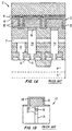
- Stacked capacitors 3 include two electrodes a top electrode or storage node 4, usually platinum (Pt) and an electrode 12 separated by a dielectric layer 18.
- An access transistor 5 includes a gate 6 which when activated electrically couples a bitline 7 through a bitline contact 8 to a plug 14.
- Plug 14 connects to electrode 12 through a diffusion barrier 16 which stores charge in electrode 12.
- FIG 1B A partial view of a conventional stacked capacitor 10 is shown in FIG 1B.
- Stacked capacitor 10 includes electrode 12, preferably formed of platinum (Pt). Electrode 12 is separated from plug 14 by diffusion barrier 16. Plug 14 is preferably polycrystalline silicon (polysilicon or poly).
- dielectric layer 18 is deposited on electrode 12. Dielectric layer 18 is typically a material with a high dielectric constant, for example BSTO. During the deposition of dielectric layer 18, oxide layers 20 and 21 form which are detrimental to the performance of the stacked capacitor. Diffusion barrier 16 is employed to prevent the formation of oxide layer 21.
- Oxide layers 20 and 21 form if:
- Oxide layers 20 and 21 reduce the capacitance of stacked capacitor 10. Therefore, a need exists for improving capacitance of stacked capacitors by eliminating oxide layers adjacent to a barrier layer formed as a result of processing and diffusion. A further need exists for a method of increasing conductivity of a plug used in stacked capacitors.
- the present invention includes a method of improving conductivity between an electrode and a plug in a stacked capacitor where an oxide has formed therebetween as defined in claim 1.
- the method includes the steps of bombarding the oxide with ions and mixing the oxide with materials of the electrode and the plug to increase a conductivity between the electrode and the plug.
- the step of bombarding may include the step of bombarding by ion implantation.
- the step of bombarding may also include the step of bombarding the oxide with germanium ions.
- the step of bombarding preferably includes the step of adjusting an angle of incident ions to provide for improved mixing.
- the step of bombarding may further include the step of adjusting an energy and dose of incident ions to provide for improved mixing.
- the electrode preferably includes platinum, and the plug preferably includes polysilicon.
- the present disclosure relates to stack capacitors for semiconductor devices and more particularly, to a high conductivity plug for transferring charge to the capacitor electrode.
- the present invention includes ion implant processes to change an oxide layer into a conductive layer or to form an oxygen diffusion barrier inside an electrode to prevent oxide layers from forming. Changing the oxide layers to conductive layers may be performed using ion implantation (I/I).
- the oxygen diffusion barrier may be formed using plasma doping (PLAD) or plasma immersion ion implantation (PIII).
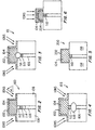
- FIG. 2 shows a stacked capacitor 100 in accordance with one aspect of the present invention.
- a plug 106 is formed inside a dielectric layer 108.
- Dielectric layer 108 may include silicon dioxide material.
- a diffusion barrier 110 is formed at a top portion of plug 106.
- Diffusion barrier 110 preferably includes TaN, CoSi, TiN, WSi, TaSiN or equivalent materials.
- An electrode 104 is formed on diffusion barrier 110.
- Electrode 104 is preferably formed from platinum although other conductive materials such as Iridium (Ir), Ruthenium (Ru) or Ruthenium oxide (RuO 2 ) may be used.
- a high dielectric constant layer 102 is deposited on electrode 104.
- High dielectric constant layer 102 is preferably formed from BSTO.
- BSTO is preferably deposited at high temperatures. However, since high temperatures increase diffusion, BSTO deposition temperatures must be limited to reduce the diffusion of materials, such as oxygen. In the present invention however deposition temperatures for layer 102 may advantageously be increased without degrading performance as explained herein.
- an oxide layer 112 and/or an oxide layer 114 are formed as described above.
- oxide layers 112 and/or 114 are conductive.
- germanium (Ge) is implanted into oxide layers 112 and/or 114.
- Other elements suitable for implantation include Si, C, and/or N.
- oxide layer 112 and/or 114 are well mixed with materials adjacent to the respective oxide layers, thereby increasing the conductivity between plug 106 and electrode 104.
- Ge is an electrically neutral element, Ge bridges the adjacent conductive layers (electrode/diffusion barrier or diffusion barrier/plug) to substantially increase conductivity between plug 106 and electrode 104.
- Ion implantation includes bombarding oxide layer 112 and/or 114 with ions having energies between about 30 and about 200 keV, preferably between about 50 and about 150 keV at doses of between about 1 ⁇ 10 10 and about 1 ⁇ 10 16 atoms/cm 2 , preferably between about 1 ⁇ 10 14 and about 1 ⁇ 10 15 atoms/cm 2 .
- ions are introduced at an angle, ⁇ , between about 30° and about 60°.
- a stacked capacitor 101 is shown after ion implantation of Ge into oxide layer 112.
- a mixed region 116 is formed wherein atoms of adjacent materials such as from electrode 104 and diffusion barrier 110 are mixed together with oxide layer 112 to form a conductive composite thereby increasing the conductivity between electrode 104 and plug 106.
- a stacked capacitor 103 is shown after ion implantation of Ge into oxide layer 114.
- a mixed region 118 is formed wherein atoms of adjacent materials such as from diffusion barrier 110 and plug 106 are mixed together with oxide layer 114 to form a conductive composite thereby increasing the conductivity between electrode 104 and plug 106.
- a diffusion barrier may be formed on or in the electrode to prevent oxygen and/or silicon from diffusing therethrough.
- Stacked capacitor 200 includes a diffusion barrier 202 which is provided and formed on electrode 104. Diffusion barrier 202 inhibits the diffusion of oxygen and silicon therethrough. Barrier 202 is formed prior to high dielectric constant layer 102 deposition (see FIG. 2) where oxygen may be introduced. Barrier 202 may be deposited on the surface of electrode 104 by a chemical vapor deposition process or by PIII or PLAD.
- barrier 202 is formed on a surface of electrode 104 to permit improved conductivity between electrode 104 and plug 106 by preventing the diffusion of oxygen to a region between electrode 104 and plug 106.
- Barrier 202 may be sized to obviate the need for diffusion barrier 110 since diffusing oxygen through dielectric layer 102, deposition is inhibited by barrier 202.
- barrier 110 may be maintained, however more materials choices are available for the diffusion barrier 110 since oxygen concentration is reduced.
- a material that is easier to process but has less oxygen diffusion inhibiting properties may be substituted.
- TiN may be used.
- a barrier 204 is formed below the surface of electrode 104.
- a diffusion inhibiting material such as nitrogen
- Barrier 204 may be positioned and sized to obviate the need for diffusion barrier 110 (FIG. 2) since diffusing oxygen from conductive layer 102 deposition is inhibited by barrier 204.
- barrier 110 may be maintained, however more materials choices are available for the diffusion barrier 110 since oxygen concentration is reduced. In this way, a more easily processed material may be substituted.
- TiN may be used.
- PIII and PLAD include bombarding electrode 104 with ions having energies between 500 eV and about 10 keV, preferably between about 1 keV and about 5 keV, at doses of between about 1 ⁇ 10 15 atoms/cm 2 and about 1 ⁇ 10 17 atoms/cm 2 , preferably between about 5 ⁇ 10 15 atoms/cm 2 and about 5 ⁇ 10 16 atoms/cm 2 . Since PIII is an isotropic process and includes three dimensional doping, ⁇ is not relevant. PIII is performed at pressures of about 5 mTorr to about 300 mTorr, preferably 20 mTorr to about 100 mTorr.
Description
Claims (7)
- A method of improving conductivity between an electrode (104) and a plug (106) in a stacked capacitor wherein said electrode (104) is one of two electrodes of said capacitor and is connected via said plug (106) to a storage node within an integrated circuit and wherein an oxide (112 and/or 114) has formed between said electrode (104) and said plug (106) comprising the steps of:bombarding the oxide with ions; andmixing the oxide with materials of the electrode and the plug to increase a conductivity between the electrode and the plug.
- The method as recited in claim 1, wherein the step of bombarding includes the step of bombarding by ion implantation.
- The method as recited in claim 1, wherein the step of bombarding includes the step of bombarding the oxide with germanium ions.
- The method as recited in claim 1, wherein the step of bombarding includes the step of adjusting an angle of incident ions to provide for improved mixing.
- The method as recited in claim 1, wherein the step of bombarding includes the step of adjusting an energy and dose of incident ions to provide for improved mixing.
- The method as recited in claim 1, wherein the electrode (104) includes platinum.
- The method as recited in claim 1, wherein the plug (106) includes polysilicon.
Applications Claiming Priority (2)
| Application Number | Priority Date | Filing Date | Title |
|---|---|---|---|
| US74882 | 1987-07-17 | ||
| US09/074,882 US6046059A (en) | 1998-05-08 | 1998-05-08 | Method of forming stack capacitor with improved plug conductivity |
Publications (3)
| Publication Number | Publication Date |
|---|---|
| EP0955679A2 EP0955679A2 (en) | 1999-11-10 |
| EP0955679A3 EP0955679A3 (en) | 2002-01-16 |
| EP0955679B1 true EP0955679B1 (en) | 2004-06-23 |
Family
ID=22122235
Family Applications (1)
| Application Number | Title | Priority Date | Filing Date |
|---|---|---|---|
| EP99107089A Expired - Lifetime EP0955679B1 (en) | 1998-05-08 | 1999-04-12 | Method of improving plug conductivity |
Country Status (7)
| Country | Link |
|---|---|
| US (2) | US6046059A (en) |
| EP (1) | EP0955679B1 (en) |
| JP (1) | JP2000031418A (en) |
| KR (1) | KR100372404B1 (en) |
| CN (1) | CN1235368A (en) |
| DE (1) | DE69918219T2 (en) |
| TW (1) | TW410429B (en) |
Families Citing this family (9)
| Publication number | Priority date | Publication date | Assignee | Title |
|---|---|---|---|---|
| US6174799B1 (en) * | 1999-01-05 | 2001-01-16 | Advanced Micro Devices, Inc. | Graded compound seed layers for semiconductors |
| US6214661B1 (en) * | 2000-01-21 | 2001-04-10 | Infineon Technologoies North America Corp. | Method to prevent oxygen out-diffusion from BSTO containing micro-electronic device |
| US6624076B1 (en) * | 2000-01-21 | 2003-09-23 | Matsushita Electric Industrial Co., Ltd. | Semiconductor device and method for fabricating the same |
| US6358855B1 (en) | 2000-06-16 | 2002-03-19 | Infineon Technologies Ag | Clean method for recessed conductive barriers |
| US6297123B1 (en) * | 2000-11-29 | 2001-10-02 | United Microelectronics Corp. | Method of preventing neck oxidation of a storage node |
| US6432725B1 (en) | 2001-09-28 | 2002-08-13 | Infineon Technologies Ag | Methods for crystallizing metallic oxide dielectric films at low temperature |
| US6515325B1 (en) | 2002-03-06 | 2003-02-04 | Micron Technology, Inc. | Nanotube semiconductor devices and methods for making the same |
| US7231839B2 (en) * | 2003-08-11 | 2007-06-19 | The Board Of Trustees Of The Leland Stanford Junior University | Electroosmotic micropumps with applications to fluid dispensing and field sampling |
| US7927948B2 (en) | 2005-07-20 | 2011-04-19 | Micron Technology, Inc. | Devices with nanocrystals and methods of formation |
Family Cites Families (7)
| Publication number | Priority date | Publication date | Assignee | Title |
|---|---|---|---|---|
| US5381302A (en) * | 1993-04-02 | 1995-01-10 | Micron Semiconductor, Inc. | Capacitor compatible with high dielectric constant materials having a low contact resistance layer and the method for forming same |
| US5504041A (en) * | 1994-08-01 | 1996-04-02 | Texas Instruments Incorporated | Conductive exotic-nitride barrier layer for high-dielectric-constant materials |
| US6093615A (en) * | 1994-08-15 | 2000-07-25 | Micron Technology, Inc. | Method of fabricating a contact structure having a composite barrier layer between a platinum layer and a polysilicon plug |
| JPH0945877A (en) * | 1995-07-31 | 1997-02-14 | Matsushita Electron Corp | Manufacture of capacitor element |
| JP3388089B2 (en) * | 1996-04-25 | 2003-03-17 | シャープ株式会社 | Method of manufacturing nonvolatile semiconductor memory device |
| KR100226772B1 (en) * | 1996-09-25 | 1999-10-15 | 김영환 | Semiconductor memory device and fabricating method thereof |
| KR100445059B1 (en) * | 1997-06-30 | 2004-11-16 | 주식회사 하이닉스반도체 | Method of fabricating capacitor of semiconductor device for improving physical property of capacitor bottom electrode |
-
1998
- 1998-05-08 US US09/074,882 patent/US6046059A/en not_active Expired - Lifetime
-
1999
- 1999-04-12 EP EP99107089A patent/EP0955679B1/en not_active Expired - Lifetime
- 1999-04-12 DE DE69918219T patent/DE69918219T2/en not_active Expired - Lifetime
- 1999-05-06 KR KR10-1999-0016143A patent/KR100372404B1/en not_active IP Right Cessation
- 1999-05-07 JP JP11127655A patent/JP2000031418A/en active Pending
- 1999-05-07 CN CN99106356A patent/CN1235368A/en active Pending
- 1999-07-06 TW TW088107286A patent/TW410429B/en not_active IP Right Cessation
-
2000
- 2000-01-06 US US09/478,312 patent/US6313495B1/en not_active Expired - Lifetime
Also Published As
| Publication number | Publication date |
|---|---|
| KR100372404B1 (en) | 2003-02-17 |
| DE69918219T2 (en) | 2005-07-28 |
| CN1235368A (en) | 1999-11-17 |
| JP2000031418A (en) | 2000-01-28 |
| US6046059A (en) | 2000-04-04 |
| KR19990088068A (en) | 1999-12-27 |
| DE69918219D1 (en) | 2004-07-29 |
| TW410429B (en) | 2000-11-01 |
| EP0955679A2 (en) | 1999-11-10 |
| EP0955679A3 (en) | 2002-01-16 |
| US6313495B1 (en) | 2001-11-06 |
Similar Documents
| Publication | Publication Date | Title |
|---|---|---|
| US6518070B1 (en) | Process of forming a semiconductor device and a semiconductor device | |
| US7446363B2 (en) | Capacitor including a percentage of amorphous dielectric material and a percentage of crystalline dielectric material | |
| US6165864A (en) | Tapered electrode for stacked capacitors | |
| US7206215B2 (en) | Antifuse having tantalum oxynitride film and method for making same | |
| US7253052B2 (en) | Method for forming a storage cell capacitor compatible with high dielectric constant materials | |
| US6475855B1 (en) | Method of forming integrated circuitry, method of forming a capacitor and method of forming DRAM integrated circuitry | |
| KR100317433B1 (en) | Semiconductor device and manufacturing method thereof | |
| US6372574B1 (en) | Method of forming a capacitor container electrode and method of patterning a metal layer by selectively silicizing the electrode or metal layer and removing the silicized portion | |
| US6077737A (en) | Method for forming a DRAM having improved capacitor dielectric layers | |
| EP0955679B1 (en) | Method of improving plug conductivity | |
| US6285038B1 (en) | Integrated circuitry and DRAM integrated circuitry | |
| US20020135010A1 (en) | Memory-storage node and the method of fabricating the same | |
| US6503810B2 (en) | Method for forming a capacitor for semiconductor devices with an amorphous LixTa1-xO3 dieletric layer having a perovskite structure | |
| US6222220B1 (en) | Extended trench for preventing interaction between components of stacked capacitors | |
| US6579755B2 (en) | High dielectric capacitor and method of manufacturing the same | |
| US6399440B1 (en) | Method to reduce the node contact resistance | |
| JPH10321816A (en) | Semiconductor device having capacitor |
Legal Events
| Date | Code | Title | Description |
|---|---|---|---|
| PUAI | Public reference made under article 153(3) epc to a published international application that has entered the european phase |
Free format text: ORIGINAL CODE: 0009012 |
|
| AK | Designated contracting states |
Kind code of ref document: A2 Designated state(s): AT BE CH CY DE DK ES FI FR GB GR IE IT LI LU MC NL PT SE Kind code of ref document: A2 Designated state(s): DE FR GB IE |
|
| AX | Request for extension of the european patent |
Free format text: AL;LT;LV;MK;RO;SI |
|
| PUAL | Search report despatched |
Free format text: ORIGINAL CODE: 0009013 |
|
| AK | Designated contracting states |
Kind code of ref document: A3 Designated state(s): AT BE CH CY DE DK ES FI FR GB GR IE IT LI LU MC NL PT SE |
|
| AX | Request for extension of the european patent |
Free format text: AL;LT;LV;MK;RO;SI |
|
| 17P | Request for examination filed |
Effective date: 20020406 |
|
| 17Q | First examination report despatched |
Effective date: 20020807 |
|
| AKX | Designation fees paid |
Free format text: DE FR GB IE |
|
| GRAP | Despatch of communication of intention to grant a patent |
Free format text: ORIGINAL CODE: EPIDOSNIGR1 |
|
| RTI1 | Title (correction) |
Free format text: METHOD OF IMPROVING PLUG CONDUCTIVITY |
|
| RTI1 | Title (correction) |
Free format text: METHOD OF IMPROVING PLUG CONDUCTIVITY |
|
| GRAS | Grant fee paid |
Free format text: ORIGINAL CODE: EPIDOSNIGR3 |
|
| RAP1 | Party data changed (applicant data changed or rights of an application transferred) |
Owner name: INFINEON TECHNOLOGIES AG |
|
| GRAA | (expected) grant |
Free format text: ORIGINAL CODE: 0009210 |
|
| AK | Designated contracting states |
Kind code of ref document: B1 Designated state(s): DE FR GB IE |
|
| PG25 | Lapsed in a contracting state [announced via postgrant information from national office to epo] |
Ref country code: FR Free format text: LAPSE BECAUSE OF FAILURE TO SUBMIT A TRANSLATION OF THE DESCRIPTION OR TO PAY THE FEE WITHIN THE PRESCRIBED TIME-LIMIT Effective date: 20040623 |
|
| REG | Reference to a national code |
Ref country code: GB Ref legal event code: FG4D |
|
| REG | Reference to a national code |
Ref country code: IE Ref legal event code: FG4D |
|
| REF | Corresponds to: |
Ref document number: 69918219 Country of ref document: DE Date of ref document: 20040729 Kind code of ref document: P |
|
| PLBE | No opposition filed within time limit |
Free format text: ORIGINAL CODE: 0009261 |
|
| STAA | Information on the status of an ep patent application or granted ep patent |
Free format text: STATUS: NO OPPOSITION FILED WITHIN TIME LIMIT |
|
| 26N | No opposition filed |
Effective date: 20050324 |
|
| EN | Fr: translation not filed | ||
| PGFP | Annual fee paid to national office [announced via postgrant information from national office to epo] |
Ref country code: GB Payment date: 20060420 Year of fee payment: 8 |
|
| REG | Reference to a national code |
Ref country code: HK Ref legal event code: WD Ref document number: 1021249 Country of ref document: HK |
|
| GBPC | Gb: european patent ceased through non-payment of renewal fee |
Effective date: 20070412 |
|
| PG25 | Lapsed in a contracting state [announced via postgrant information from national office to epo] |
Ref country code: GB Free format text: LAPSE BECAUSE OF NON-PAYMENT OF DUE FEES Effective date: 20070412 |
|
| PGFP | Annual fee paid to national office [announced via postgrant information from national office to epo] |
Ref country code: IE Payment date: 20080424 Year of fee payment: 10 |
|
| REG | Reference to a national code |
Ref country code: IE Ref legal event code: MM4A |
|
| PG25 | Lapsed in a contracting state [announced via postgrant information from national office to epo] |
Ref country code: IE Free format text: LAPSE BECAUSE OF NON-PAYMENT OF DUE FEES Effective date: 20090413 |
|
| REG | Reference to a national code |
Ref country code: DE Ref legal event code: R081 Ref document number: 69918219 Country of ref document: DE Owner name: POLARIS INNOVATIONS LTD., IE Free format text: FORMER OWNER: QIMONDA AG, 81739 MUENCHEN, DE Ref country code: DE Ref legal event code: R081 Ref document number: 69918219 Country of ref document: DE Owner name: INFINEON TECHNOLOGIES AG, DE Free format text: FORMER OWNER: QIMONDA AG, 81739 MUENCHEN, DE |
|
| REG | Reference to a national code |
Ref country code: DE Ref legal event code: R081 Ref document number: 69918219 Country of ref document: DE Owner name: POLARIS INNOVATIONS LTD., IE Free format text: FORMER OWNER: INFINEON TECHNOLOGIES AG, 85579 NEUBIBERG, DE |
|
| PGFP | Annual fee paid to national office [announced via postgrant information from national office to epo] |
Ref country code: DE Payment date: 20180327 Year of fee payment: 20 |
|
| REG | Reference to a national code |
Ref country code: DE Ref legal event code: R071 Ref document number: 69918219 Country of ref document: DE |