EP0932193A2 - Method of forming bump electrodes - Google Patents
Method of forming bump electrodes Download PDFInfo
- Publication number
- EP0932193A2 EP0932193A2 EP99101055A EP99101055A EP0932193A2 EP 0932193 A2 EP0932193 A2 EP 0932193A2 EP 99101055 A EP99101055 A EP 99101055A EP 99101055 A EP99101055 A EP 99101055A EP 0932193 A2 EP0932193 A2 EP 0932193A2
- Authority
- EP
- European Patent Office
- Prior art keywords
- electrode formation
- bump electrode
- wafer
- paste
- formation surface
- Prior art date
- Legal status (The legal status is an assumption and is not a legal conclusion. Google has not performed a legal analysis and makes no representation as to the accuracy of the status listed.)
- Withdrawn
Links
Images


Classifications
-
- H—ELECTRICITY
- H01—ELECTRIC ELEMENTS
- H01L—SEMICONDUCTOR DEVICES NOT COVERED BY CLASS H10
- H01L24/00—Arrangements for connecting or disconnecting semiconductor or solid-state bodies; Methods or apparatus related thereto
- H01L24/01—Means for bonding being attached to, or being formed on, the surface to be connected, e.g. chip-to-package, die-attach, "first-level" interconnects; Manufacturing methods related thereto
- H01L24/10—Bump connectors ; Manufacturing methods related thereto
- H01L24/11—Manufacturing methods
-
- H—ELECTRICITY
- H01—ELECTRIC ELEMENTS
- H01L—SEMICONDUCTOR DEVICES NOT COVERED BY CLASS H10
- H01L24/00—Arrangements for connecting or disconnecting semiconductor or solid-state bodies; Methods or apparatus related thereto
- H01L24/01—Means for bonding being attached to, or being formed on, the surface to be connected, e.g. chip-to-package, die-attach, "first-level" interconnects; Manufacturing methods related thereto
- H01L24/10—Bump connectors ; Manufacturing methods related thereto
- H01L24/12—Structure, shape, material or disposition of the bump connectors prior to the connecting process
- H01L24/13—Structure, shape, material or disposition of the bump connectors prior to the connecting process of an individual bump connector
-
- H—ELECTRICITY
- H05—ELECTRIC TECHNIQUES NOT OTHERWISE PROVIDED FOR
- H05K—PRINTED CIRCUITS; CASINGS OR CONSTRUCTIONAL DETAILS OF ELECTRIC APPARATUS; MANUFACTURE OF ASSEMBLAGES OF ELECTRICAL COMPONENTS
- H05K3/00—Apparatus or processes for manufacturing printed circuits
- H05K3/10—Apparatus or processes for manufacturing printed circuits in which conductive material is applied to the insulating support in such a manner as to form the desired conductive pattern
- H05K3/20—Apparatus or processes for manufacturing printed circuits in which conductive material is applied to the insulating support in such a manner as to form the desired conductive pattern by affixing prefabricated conductor pattern
- H05K3/207—Apparatus or processes for manufacturing printed circuits in which conductive material is applied to the insulating support in such a manner as to form the desired conductive pattern by affixing prefabricated conductor pattern using a prefabricated paste pattern, ink pattern or powder pattern
-
- H—ELECTRICITY
- H01—ELECTRIC ELEMENTS
- H01L—SEMICONDUCTOR DEVICES NOT COVERED BY CLASS H10
- H01L2224/00—Indexing scheme for arrangements for connecting or disconnecting semiconductor or solid-state bodies and methods related thereto as covered by H01L24/00
- H01L2224/01—Means for bonding being attached to, or being formed on, the surface to be connected, e.g. chip-to-package, die-attach, "first-level" interconnects; Manufacturing methods related thereto
- H01L2224/02—Bonding areas; Manufacturing methods related thereto
- H01L2224/04—Structure, shape, material or disposition of the bonding areas prior to the connecting process
- H01L2224/06—Structure, shape, material or disposition of the bonding areas prior to the connecting process of a plurality of bonding areas
- H01L2224/061—Disposition
- H01L2224/0612—Layout
- H01L2224/0613—Square or rectangular array
- H01L2224/06131—Square or rectangular array being uniform, i.e. having a uniform pitch across the array
-
- H—ELECTRICITY
- H01—ELECTRIC ELEMENTS
- H01L—SEMICONDUCTOR DEVICES NOT COVERED BY CLASS H10
- H01L2224/00—Indexing scheme for arrangements for connecting or disconnecting semiconductor or solid-state bodies and methods related thereto as covered by H01L24/00
- H01L2224/01—Means for bonding being attached to, or being formed on, the surface to be connected, e.g. chip-to-package, die-attach, "first-level" interconnects; Manufacturing methods related thereto
- H01L2224/10—Bump connectors; Manufacturing methods related thereto
- H01L2224/1012—Auxiliary members for bump connectors, e.g. spacers
- H01L2224/10152—Auxiliary members for bump connectors, e.g. spacers being formed on an item to be connected not being a semiconductor or solid-state body
- H01L2224/10165—Alignment aids
-
- H—ELECTRICITY
- H01—ELECTRIC ELEMENTS
- H01L—SEMICONDUCTOR DEVICES NOT COVERED BY CLASS H10
- H01L2224/00—Indexing scheme for arrangements for connecting or disconnecting semiconductor or solid-state bodies and methods related thereto as covered by H01L24/00
- H01L2224/01—Means for bonding being attached to, or being formed on, the surface to be connected, e.g. chip-to-package, die-attach, "first-level" interconnects; Manufacturing methods related thereto
- H01L2224/10—Bump connectors; Manufacturing methods related thereto
- H01L2224/11—Manufacturing methods
- H01L2224/113—Manufacturing methods by local deposition of the material of the bump connector
- H01L2224/1133—Manufacturing methods by local deposition of the material of the bump connector in solid form
- H01L2224/1134—Stud bumping, i.e. using a wire-bonding apparatus
-
- H—ELECTRICITY
- H01—ELECTRIC ELEMENTS
- H01L—SEMICONDUCTOR DEVICES NOT COVERED BY CLASS H10
- H01L2224/00—Indexing scheme for arrangements for connecting or disconnecting semiconductor or solid-state bodies and methods related thereto as covered by H01L24/00
- H01L2224/01—Means for bonding being attached to, or being formed on, the surface to be connected, e.g. chip-to-package, die-attach, "first-level" interconnects; Manufacturing methods related thereto
- H01L2224/10—Bump connectors; Manufacturing methods related thereto
- H01L2224/12—Structure, shape, material or disposition of the bump connectors prior to the connecting process
- H01L2224/13—Structure, shape, material or disposition of the bump connectors prior to the connecting process of an individual bump connector
- H01L2224/13001—Core members of the bump connector
- H01L2224/13099—Material
-
- H—ELECTRICITY
- H01—ELECTRIC ELEMENTS
- H01L—SEMICONDUCTOR DEVICES NOT COVERED BY CLASS H10
- H01L2224/00—Indexing scheme for arrangements for connecting or disconnecting semiconductor or solid-state bodies and methods related thereto as covered by H01L24/00
- H01L2224/80—Methods for connecting semiconductor or other solid state bodies using means for bonding being attached to, or being formed on, the surface to be connected
- H01L2224/81—Methods for connecting semiconductor or other solid state bodies using means for bonding being attached to, or being formed on, the surface to be connected using a bump connector
- H01L2224/8112—Aligning
- H01L2224/81136—Aligning involving guiding structures, e.g. spacers or supporting members
- H01L2224/81138—Aligning involving guiding structures, e.g. spacers or supporting members the guiding structures being at least partially left in the finished device
- H01L2224/8114—Guiding structures outside the body
-
- H—ELECTRICITY
- H01—ELECTRIC ELEMENTS
- H01L—SEMICONDUCTOR DEVICES NOT COVERED BY CLASS H10
- H01L2924/00—Indexing scheme for arrangements or methods for connecting or disconnecting semiconductor or solid-state bodies as covered by H01L24/00
- H01L2924/0001—Technical content checked by a classifier
-
- H—ELECTRICITY
- H01—ELECTRIC ELEMENTS
- H01L—SEMICONDUCTOR DEVICES NOT COVERED BY CLASS H10
- H01L2924/00—Indexing scheme for arrangements or methods for connecting or disconnecting semiconductor or solid-state bodies as covered by H01L24/00
- H01L2924/01—Chemical elements
- H01L2924/01005—Boron [B]
-
- H—ELECTRICITY
- H01—ELECTRIC ELEMENTS
- H01L—SEMICONDUCTOR DEVICES NOT COVERED BY CLASS H10
- H01L2924/00—Indexing scheme for arrangements or methods for connecting or disconnecting semiconductor or solid-state bodies as covered by H01L24/00
- H01L2924/01—Chemical elements
- H01L2924/01006—Carbon [C]
-
- H—ELECTRICITY
- H01—ELECTRIC ELEMENTS
- H01L—SEMICONDUCTOR DEVICES NOT COVERED BY CLASS H10
- H01L2924/00—Indexing scheme for arrangements or methods for connecting or disconnecting semiconductor or solid-state bodies as covered by H01L24/00
- H01L2924/01—Chemical elements
- H01L2924/01022—Titanium [Ti]
-
- H—ELECTRICITY
- H01—ELECTRIC ELEMENTS
- H01L—SEMICONDUCTOR DEVICES NOT COVERED BY CLASS H10
- H01L2924/00—Indexing scheme for arrangements or methods for connecting or disconnecting semiconductor or solid-state bodies as covered by H01L24/00
- H01L2924/01—Chemical elements
- H01L2924/01029—Copper [Cu]
-
- H—ELECTRICITY
- H01—ELECTRIC ELEMENTS
- H01L—SEMICONDUCTOR DEVICES NOT COVERED BY CLASS H10
- H01L2924/00—Indexing scheme for arrangements or methods for connecting or disconnecting semiconductor or solid-state bodies as covered by H01L24/00
- H01L2924/01—Chemical elements
- H01L2924/01033—Arsenic [As]
-
- H—ELECTRICITY
- H01—ELECTRIC ELEMENTS
- H01L—SEMICONDUCTOR DEVICES NOT COVERED BY CLASS H10
- H01L2924/00—Indexing scheme for arrangements or methods for connecting or disconnecting semiconductor or solid-state bodies as covered by H01L24/00
- H01L2924/01—Chemical elements
- H01L2924/01039—Yttrium [Y]
-
- H—ELECTRICITY
- H01—ELECTRIC ELEMENTS
- H01L—SEMICONDUCTOR DEVICES NOT COVERED BY CLASS H10
- H01L2924/00—Indexing scheme for arrangements or methods for connecting or disconnecting semiconductor or solid-state bodies as covered by H01L24/00
- H01L2924/01—Chemical elements
- H01L2924/01046—Palladium [Pd]
-
- H—ELECTRICITY
- H01—ELECTRIC ELEMENTS
- H01L—SEMICONDUCTOR DEVICES NOT COVERED BY CLASS H10
- H01L2924/00—Indexing scheme for arrangements or methods for connecting or disconnecting semiconductor or solid-state bodies as covered by H01L24/00
- H01L2924/01—Chemical elements
- H01L2924/01047—Silver [Ag]
-
- H—ELECTRICITY
- H01—ELECTRIC ELEMENTS
- H01L—SEMICONDUCTOR DEVICES NOT COVERED BY CLASS H10
- H01L2924/00—Indexing scheme for arrangements or methods for connecting or disconnecting semiconductor or solid-state bodies as covered by H01L24/00
- H01L2924/01—Chemical elements
- H01L2924/01078—Platinum [Pt]
-
- H—ELECTRICITY
- H01—ELECTRIC ELEMENTS
- H01L—SEMICONDUCTOR DEVICES NOT COVERED BY CLASS H10
- H01L2924/00—Indexing scheme for arrangements or methods for connecting or disconnecting semiconductor or solid-state bodies as covered by H01L24/00
- H01L2924/01—Chemical elements
- H01L2924/01079—Gold [Au]
-
- H—ELECTRICITY
- H01—ELECTRIC ELEMENTS
- H01L—SEMICONDUCTOR DEVICES NOT COVERED BY CLASS H10
- H01L2924/00—Indexing scheme for arrangements or methods for connecting or disconnecting semiconductor or solid-state bodies as covered by H01L24/00
- H01L2924/01—Chemical elements
- H01L2924/01082—Lead [Pb]
-
- H—ELECTRICITY
- H01—ELECTRIC ELEMENTS
- H01L—SEMICONDUCTOR DEVICES NOT COVERED BY CLASS H10
- H01L2924/00—Indexing scheme for arrangements or methods for connecting or disconnecting semiconductor or solid-state bodies as covered by H01L24/00
- H01L2924/013—Alloys
- H01L2924/0132—Binary Alloys
- H01L2924/01322—Eutectic Alloys, i.e. obtained by a liquid transforming into two solid phases
-
- H—ELECTRICITY
- H01—ELECTRIC ELEMENTS
- H01L—SEMICONDUCTOR DEVICES NOT COVERED BY CLASS H10
- H01L2924/00—Indexing scheme for arrangements or methods for connecting or disconnecting semiconductor or solid-state bodies as covered by H01L24/00
- H01L2924/013—Alloys
- H01L2924/014—Solder alloys
-
- H—ELECTRICITY
- H01—ELECTRIC ELEMENTS
- H01L—SEMICONDUCTOR DEVICES NOT COVERED BY CLASS H10
- H01L2924/00—Indexing scheme for arrangements or methods for connecting or disconnecting semiconductor or solid-state bodies as covered by H01L24/00
- H01L2924/10—Details of semiconductor or other solid state devices to be connected
- H01L2924/11—Device type
- H01L2924/12—Passive devices, e.g. 2 terminal devices
- H01L2924/1204—Optical Diode
- H01L2924/12042—LASER
-
- H—ELECTRICITY
- H01—ELECTRIC ELEMENTS
- H01L—SEMICONDUCTOR DEVICES NOT COVERED BY CLASS H10
- H01L2924/00—Indexing scheme for arrangements or methods for connecting or disconnecting semiconductor or solid-state bodies as covered by H01L24/00
- H01L2924/10—Details of semiconductor or other solid state devices to be connected
- H01L2924/11—Device type
- H01L2924/14—Integrated circuits
-
- H—ELECTRICITY
- H01—ELECTRIC ELEMENTS
- H01L—SEMICONDUCTOR DEVICES NOT COVERED BY CLASS H10
- H01L2924/00—Indexing scheme for arrangements or methods for connecting or disconnecting semiconductor or solid-state bodies as covered by H01L24/00
- H01L2924/19—Details of hybrid assemblies other than the semiconductor or other solid state devices to be connected
- H01L2924/1901—Structure
- H01L2924/1904—Component type
- H01L2924/19041—Component type being a capacitor
-
- H—ELECTRICITY
- H01—ELECTRIC ELEMENTS
- H01L—SEMICONDUCTOR DEVICES NOT COVERED BY CLASS H10
- H01L2924/00—Indexing scheme for arrangements or methods for connecting or disconnecting semiconductor or solid-state bodies as covered by H01L24/00
- H01L2924/30—Technical effects
- H01L2924/301—Electrical effects
- H01L2924/3025—Electromagnetic shielding
-
- H—ELECTRICITY
- H01—ELECTRIC ELEMENTS
- H01L—SEMICONDUCTOR DEVICES NOT COVERED BY CLASS H10
- H01L2924/00—Indexing scheme for arrangements or methods for connecting or disconnecting semiconductor or solid-state bodies as covered by H01L24/00
- H01L2924/30—Technical effects
- H01L2924/35—Mechanical effects
- H01L2924/351—Thermal stress
- H01L2924/3511—Warping
-
- H—ELECTRICITY
- H05—ELECTRIC TECHNIQUES NOT OTHERWISE PROVIDED FOR
- H05K—PRINTED CIRCUITS; CASINGS OR CONSTRUCTIONAL DETAILS OF ELECTRIC APPARATUS; MANUFACTURE OF ASSEMBLAGES OF ELECTRICAL COMPONENTS
- H05K2201/00—Indexing scheme relating to printed circuits covered by H05K1/00
- H05K2201/03—Conductive materials
- H05K2201/0332—Structure of the conductor
- H05K2201/0364—Conductor shape
- H05K2201/0367—Metallic bump or raised conductor not used as solder bump
-
- H—ELECTRICITY
- H05—ELECTRIC TECHNIQUES NOT OTHERWISE PROVIDED FOR
- H05K—PRINTED CIRCUITS; CASINGS OR CONSTRUCTIONAL DETAILS OF ELECTRIC APPARATUS; MANUFACTURE OF ASSEMBLAGES OF ELECTRICAL COMPONENTS
- H05K2203/00—Indexing scheme relating to apparatus or processes for manufacturing printed circuits covered by H05K3/00
- H05K2203/01—Tools for processing; Objects used during processing
- H05K2203/0104—Tools for processing; Objects used during processing for patterning or coating
- H05K2203/0113—Female die used for patterning or transferring, e.g. temporary substrate having recessed pattern
-
- H—ELECTRICITY
- H05—ELECTRIC TECHNIQUES NOT OTHERWISE PROVIDED FOR
- H05K—PRINTED CIRCUITS; CASINGS OR CONSTRUCTIONAL DETAILS OF ELECTRIC APPARATUS; MANUFACTURE OF ASSEMBLAGES OF ELECTRICAL COMPONENTS
- H05K3/00—Apparatus or processes for manufacturing printed circuits
- H05K3/10—Apparatus or processes for manufacturing printed circuits in which conductive material is applied to the insulating support in such a manner as to form the desired conductive pattern
- H05K3/12—Apparatus or processes for manufacturing printed circuits in which conductive material is applied to the insulating support in such a manner as to form the desired conductive pattern using thick film techniques, e.g. printing techniques to apply the conductive material or similar techniques for applying conductive paste or ink patterns
- H05K3/1216—Apparatus or processes for manufacturing printed circuits in which conductive material is applied to the insulating support in such a manner as to form the desired conductive pattern using thick film techniques, e.g. printing techniques to apply the conductive material or similar techniques for applying conductive paste or ink patterns by screen printing or stencil printing
- H05K3/1233—Methods or means for supplying the conductive material and for forcing it through the screen or stencil
Definitions
- the present invention relates to a method of forming a plurality of bump electrodes en bloc on a bump electrode formation surface of a wafer from which chips are to be separated, or on a bump electrode formation surface on an upper surface side of a plurality of chips which are separated from a wafer and placed side by side, specifically for use in condenser chips, resistance chips, IC chips, and CPU chips, which are mounted on a surface of electronic parts, and for use in packages semi-conductor-molded ball grid arrays (BGA) and chip size packages (CSP) and connectors.
- BGA semi-conductor-molded ball grid arrays
- CSP chip size packages
- the above-mentioned chips are mounted on a surface of a substrate via bump electrodes.
- electronic chips such as IC and LSI chips are mounted on the surface of electronic parts via bump electrodes as flip chips without being packaged.
- bump electrodes be formed on the side of such electronic parts.
- the above-mentioned bump electrodes are formed on the surface of the above-mentioned electronic parts by an electrolytic plating method comprising the steps of forming a predetermined resist pattern on the surface of electronic parts by photolithography, and having the resist pattern grown to a predetermined thickness, using solder, or a metal such as gold or copper, or by a ball bump method of forming metal balls from a metal wire, and bonding the metal balls to electronic parts.
- solder or a metal such as gold or copper
- a ball bump method of forming metal balls from a metal wire
- a second object of the present invention is to provide a method of forming a plurality of bump electrodes en bloc on an upper surface of a plurality of chips which are separated from a wafer and placed side by side, the upper surface constituting a bump electrode formation surface.
- the first object of the present invention can be achieved by a method of forming a plurality of bump electrodes en bloc on a bump electrode formation surface of a wafer from which chips are to be separated, comprising the steps of:
- the stencil mask comprise a light-shielding layer at least on such a side of the stencil mask that comes into close contact with the bump electrode formation surface of the wafer, and that the photo-setting paste filled in the through-holes be exposed to light and cured, and that the stencil mask be then separated from the bump electrode formation surface of the wafer so as to fix the cured photo-setting paste to the bump electrode formation surface of the wafer for the formation of the bump electrodes en bloc thereon.
- micro-bump electrodes can be formed with high accuracy by the provision of the light-shielding layer at least on such a side of the stencil mask that comes into close contact with the bump electrode formation surface of the wafer.
- the stencil mask may comprise a plastic material that can be selectively subjected to abrasion working by light irradiation, for instance, visible light irradiation or ultraviolet light irradiation, so as to form the through-holes in the stencil mask.
- light irradiation for instance, visible light irradiation or ultraviolet light irradiation
- through-holes with a smooth inner wall can be formed from which the electroconductive paste can be smoothly released, whereby high quality bump electrodes free of defects can be formed.
- the electronductive paste may be an elastomer resin paste.
- an elastomer resin paste is used as the electroconductive paste, there can be formed such bump electrodes that comprise a highly elastic elastomer resin and are not cracked even when subjected to repeated thermal expansion and contraction.
- each of the bump electrodes may have a thin or conical top edge.
- the first object of the present invention can also be achieved by a method of forming a plurality of bump electrodes en bloc on a bump electrode formation surface of a wafer from which chips are to be separated, comprising the steps of:
- the electroconductive paste may be a photo-setting paste
- the intaglio printing mask be transparent so as to allow light to pass at least through the depressed portions of the intaglio printing mask, thereby curing the photo-setting paste in the depressed portions when exposed to light, and comprise a light-shielding layer at least on such a side of the intaglio printing mask that comes into close contact with the bump electrode formation surface of the wafer, and that the photo-setting paste be filled in the depressed portions, exposed to light and cured, and that the intaglio printing mask be then separated from the bump electrode formation surface of the wafer so as to fix the cured photo-setting paste to the bump electrode formation surface of the wafer for the formation of the bump electrodes en bloc thereon.
- the intaglio printing mask may comprise a plastic material that can be selectively subjected to abrasion working by light irradiation so as to form the depressed portions in the intaglio printing mask.
- the electronductive paste may be an elastomer resin paste for the same reasons as in the above-mentioned method using the stencil mask with the through-holes.
- each of the bump electrodes may have a thin or conical top edge for the same reasons as in the above-mentioned method using the stencil mask with the through-holes.
- the first object of the present invention can also be achieved by a method of forming a plurality of bump electrodes en bloc on a bump electrode formation surface of a wafer from which chips are to be separated, comprising the steps of:
- the electroconductive photosensitive layer may be successively exposed to light through the photo mask for the formation of the bump electrodes en bloc, while a predetermined positional registration of the photo mask relative to the bump electrode formation surface of the wafer is maintained.
- the bump electrodes can be formed with high precision with respect to the relative positions thereof.
- the second object of the present invention can be achieved by a method of forming a plurality of bump electrodes en bloc on an upper surface of a plurality of chips which are separated from a wafer and placed side by side, the upper surface constituting a bump electrode formation surface, comprising the steps of:
- the stencil mask comprise a light-shielding layer at least on such a side of the stencil mask that comes into close contact with the bump electrode formation surface of the wafer, and that the photo-setting paste filled in the through-holes be exposed to light and cured, and that the stencil mask be then separated from the bump electrode formation surface of the wafer so as to fix the cured photo-setting paste to the bump electrode formation surface of the wafer for the formation of the bump electrodes en bloc thereon.
- micro-bump electrodes can be formed with high accuracy by the provision of the light-shielding layer at least on such a side of the stencil mask that comes into close contact with the bump electrode formation surface of the wafer.
- the stencil mask may comprise a plastic material that can be selectively subjected to abrasion working light irradiation, for example, by visible light irradiation or ultraviolet light irradiation, so as to form the through-holes in the stencil mask.
- abrasion working light irradiation for example, by visible light irradiation or ultraviolet light irradiation
- the stencil mask may comprise a plastic material that can be selectively subjected to abrasion working light irradiation, for example, by visible light irradiation or ultraviolet light irradiation, so as to form the through-holes in the stencil mask.
- the electronductive paste may be an elastomer resin paste.
- an elastomer resin paste is used as the electroconductive paste, there can be formed such bump electrodes that comprise a highly elastic elastomer resin and are not cracked even when subjected to repeated thermal expansion and contraction.
- each of the bump electrodes may have a thin or conical top edge.
- the second object of the present invention can also be achieved by a method of forming a plurality of bump electrodes en bloc on an upper surface of a plurality of chips which are separated from a wafer and placed side by side, the upper surface constituting a bump electrode formation surface, comprising the steps of:
- the electroconductive paste may be a photo-setting paste
- the intaglio printing mask be transparent so as to allow light to pass at least through the depressed portions of the intaglio printing mask, thereby curing the photo-setting paste in the depressed portions when exposed to light, and comprise a light-shielding layer at least on such a side of the intaglio printing mask that comes into close contact with the bump electrode formation surface, and that the photo-setting paste be filled in the depressed portions, exposed to light and cured, and that the intaglio printing mask be then separated from the bump electrode formation surface of the wafer so as to fix the cured photo-setting paste to the bump eiectrode formation surface for the formation of the bump electrodes en bloc thereon.
- the intaglio printing mask may comprise a plastic material that can be selectively subjected to abrasion working by light irradiation, for example, by visible light irradiation or ultraviolet light irradiation, so as to form the depressed portions in the intaglio printing mask.
- a plastic material in the intaglio printing mask, depressed portions with a smooth inner wall and a bottom can be formed, from which the electroconductive paste can be smoothly released, whereby high quality bump electrodes free of defects can be formed.
- the electronductive paste may be an elastomer resin paste for the same reasons as in the above-mentioned method using the stencil mask.
- each of the bump electrodes may have a thin or conical top edge for the same reasons as in the above-mentioned method, using the stencil mask.
- the second object of the present invention can also be achieved by a method of forming a plurality of bump electrodes en bloc on an upper surface of a plurality of chips which are separated from a wafer and placed side by side, the upper surface constituting a bump electrode formation surface, comprising the steps of:
- the electroconductive photosensitive layer may be successively exposed to light through the photo mask for the formation of the bump electrodes en bloc, while a predetermined positional registration of the photo mask relative to the bump electrode formation surface of the wafer is maintained.
- the bump electrodes can be formed with high precision with the respective positions.
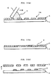
- FIG. 1(a) is a schematic plan view of a wafer 1 from which semiconductor chips 4 are to be separated, with bump electrodes 2 being formed en bloc on a bump electrode formation surface of the wafer 1 by a bump electrode formation method of the present invention.
- FIG. 1(b) is a schematic perspective view of the wafer 1 from which semiconductor chips 4 are separated.
- FIG. 1(c) is a perspective view of the separated semiconductor chip 4 on which the bump electrodes are formed by the method of the present invention.
- FIGS. 2(a) and 2(b) are diagrams in explanation of a first example of a bump electrode formation method of the present invention.
- FIGS. 3(a) to 3(c) are diagrams in explanation of a modified first example of a bump electrode formation method of the present invention.
- FIG. 4 is a diagram in explanation of a second example of a bump electrode formation method of the present invention.
- FIG. 5 is a schematic diagram in explanation of a third example of a bump electrode formation method of the present invention, using a bump electrode formation apparatus.
- FIG. 6 is an enlarged schematic diagram in explanation of an exposure step and a curing step in a transfer process in the bump electrode formation apparatus shown in FIG. 5 in the third example of the bump electrode formation method of the present invention.
- FIG. 7(a) and FIG. 7(b) are schematic diagrams in explanation of methods of forming depressed portions in a plastic material by abrasion working, using an exima laser to prepare an intaglio printing mask.
- FIG. 8(a) and FIG. 8(b) are schematic diagrams in explanation of the effects of a conical bump electrode with an acute top angle.
- FIG. 9(a) and FIG. 9(b) are schematic diagrams in explanation of the formation of pillar-shaped bump electrodes.
- FIG. 10(a) is a schematic perspective view of a tray for registration of chips.
- FIG. 10(b) is a schematic partial cross-sectional view of the tray, showing that the chips are fitted in the depressed portions of the tray shown in FIG. 10(a).
- FIG. 10(c) is a schematic partial perspective view of the tray, showing that the chips are fitted in the depressed portions of the tray shown in FIG. 10(a).
- FIG. 10 (d) is a schematic plan view of the chips placed in the depressed portions of the tray for accurate registration thereof, using registration guide members.
- a plurality of bump electrodes can be formed en bloc, for instance, on a bump electrode formation surface of a wafer from which chips such as semiconductor chips are to be separated, or on an upper surface of a plurity of chips which are separated from a wafer and placed side by side, the upper surface constituting a bump electrode formation surface.
- FIG. 1(a) shows a wafer 1 from which semiconductor chips 4 are to be separated.
- bump electrodes 2 On a bump electrode formation surface of the wafer 1 are formed bump electrodes 2 en bloc by a bump electrode formation method of the present invention.
- the wafer 1 on which the bump electrodes 2 are formed en bloc is then cut by a dicing saw 3 as illustrated in FIG. 1(c) so as to be separated into semiconductor chips 4 as illustrated in FIG. 1(c), which can be mounted on a substrate.
- FIG. 2(a) is a diagram in explanation of a first example of the method of forming the bump electrodes 2 on the wafer 1 of the present invention.
- a stencil mask 5 with through-holes 5a for the formation of bump electrodes is mounted on a bump electrode formation surface of a wafer 1 from which semiconductor chips 4 are to be separated.
- An electroconductive paste 7 containing therein fine particles with a particle diameter of 20 ⁇ m or less is brought into pressure contact with an upper surface of the stencil mask 5 with the through-holes 5a, using a squeegee 6 which is moved in the direction of the arrow along an upper surface of the stencil mask 5, whereby the through-holes 5a are filled with the electroconductive paste 7.
- the stencil mask 5 is then removed from the wafer 1 in such a manner that the electroconductive paste 7 is printed in the form of bump electrodes 2 on the bump electrode formation surface of the wafer 1 as illustrated in FIG. 2(b).
- the electroconductive paste 5 printed in the form of bump electrodes 2 on the bump electrode formation surface of the wafer 1 may be then subjected to reflow processing.
- the electroconductive paste 7 filled in the through-holes 5a of the stencil mask 5 be cured to form bump electrodes 2 en bloc before the stencil mask 5 is separated from the bump electrode formation surface of the wafer I as illustrated in FIG. 3(a) to FIG. 3(c).
- thermosetting paste which can be cured by the application of heat thereto, or a photo-setting paste which can be cured by the exposure thereof to light.
- electroconductive paste 7 for use in the present invention a two-part electroconductive paste can also be employed, which can be cured chemically with time.
- the stencil mask 5 is separated from the bump electrode formation surface of the wafer 1, so that the bump electrodes 2 can be formed en bloc on the bump electrode formation surface of the wafer 1 as illustrated in FIG. 3(a) to FIG. 3(c).
- the stencil mask 5 comprise a light-shielding layer at least on such a side of the stencil mask 5 that comes into close contact with the bump electrode formation surface of the wafer I, since by the provision of the light-shielding layer at least on such a side of the stencil mask 5 that comes into close contact with the bump electrode formation surface of the wafer 1, micro-bump electrodes can be formed en bloc with high accuracy.
- the stencil mask may comprise a plastic material that can be selectively subjected to abrasion working by light irradiation so as to form said through-holes in said stencil mask.
- the electronductive paste may be an elastomer resin paste.
- FIG. 4 is a diagram in explanation of a second example of the method of forming bump electrodes of the present invention.
- a lower portion of an airtight housing 101 constitutes a fused metal container 102 in which a fused metal 103, such as a eutectic solider or a high-temperature solider, serving as a material for the formation of the bump electrodes, is held at a fused temperature thereof, for example, at 183°C, or above,
- a fused metal 103 such as a eutectic solider or a high-temperature solider, serving as a material for the formation of the bump electrodes
- an inert gas 104 such as nitrogen gas for preventing the oxidation of the fused metal 103 is filled.
- Step A in FIG. 4 an intaglio printing mask 105 made of a plastic material with slight elasticity, having depressed portions 106 in a female die shape of the bump electrodes 2, is placed in the inert gas 104 within the airtight housing 101.
- gases remaining in the depressed portions 106 of the intaglio printing mask 105 are removed therefrom.
- the thus deaerated intaglio printing mask 105 is then immersed in the fused metal 103.
- the pressure of the inert gas 104 is then increased by the pressure increasing and decreasing apparatus 107, whereby pressure is applied to the fused metal 103, so that the depressed portions 106 are completely filled with the fused metal 103 without any unfilled space in the depressed portions 106 of the intaglio printing mask 105.
- step B after the complete filling of the fused metal 103 in the depressed portions 106 of the intaglio printing mask 105, a shielding plate 108 having a flat contact surface is brought into close and sliding contact with the surface of the intaglio printing mask 105 in such a manner that the flat contact surface of the shielding plate 108 comes into contact with the surface of the intaglio printing mask 105 on the side of the openings of the depressed portions 106 of the intaglio printing mask 105, thereby removing therefrom the fused metal 103 which stays on the surface of the intaglio printing mask 105, closing the openings of the depressed portions 106 of the intaglio printing mask 105 with the shielding plate 108, whereby the fused metal 103 is completely removed from between the surface of the intaglio printing mask 105 and the shielding plate 108, and a constant amount of the fused metal 103 is always filled in the depressed portions 106.
- Step C the intaglio printing mask 105 with the fused metal 103 being filled in the depressed portions 106 thereof is taken out from the fused metal 103, together with the shielding plate 108 which is closely attached to the printing mask 105, and then the intaglio printing mask 105 is horizontally positioned in such a posture that the depressed portions 106 filled with a fused metal 109 is directed upward.
- the shielding plate 108 is then slid and removed from the intaglio printing mask 105.
- Step D a wafer 1 from which chips are to be separated is preheated for easing heat shock, and with the bump electrode formation surface thereof being directed downward, is then brought into close contact with the intaglio printing mask 105 at a predetermined position, and is turned upside-down. Slight pressure is applied to the intaglio printing mask 105 and the wafer 1 by a pressure application apparatus 111. Due to the elasticity of the intaglio printing mask 105 made of a plastic material, the fused metal 109 filled in the depressed portions 106 of the intaglio printing mask 105 is securely brought into close contact with the wafer 1.
- Step E the intaglio printing mask 105 and the wafer 1 are gradually cooled, and after the fused metal 109 in the depressed portions 106 is solidified, the intaglio printing mask 105 is separated from the wafer 1, whereby the fused metal 109 filled in the depressed portions 106 of the intaglio printing mask 105 is transferred in the printing shape corresponding to the shape of the depressed portions 106 to the wafer 1.
- the bump electrodes for connection of flip chips can be uniformly formed en bloc on the bump electrode formation surface of the wafer 1 at low cost.
- the depressed portions 106 of the intaglio printing mask 105 can be formed by various methods such as mechanical working, photolithography, and plating.
- these methods have the shortcomings that the finer the bumps, the more difficult the production, and the higher the production cost.
- These problems can be solved by forming the depressed portions 106 in a printing shape in such a plastic plate that can be subjected to abrasion working, using visible light or ultraviolet light such as exima laser.
- Fine and small bump female die portions and grooves corresponding to fine bump electrodes, depressed below the surface of the plastic plate, can be precisely formed by exima laser engraving work.
- a material for the intaglio printing mask 105 for use in the present invention have substantially the same coefficient of thermal expansion as that of the material on which the bump electrodes are to be formed en bloc.
- the intaglio printing mask 105 be made of a metal material such as Kovar.
- the intaglio printing mask 105 may be made of such an elastic material that can be deformed, following the thermal deformation of the wafer serving as the material on which the bump electrodes are to be formed, even when the wafer is thermally expanded.
- electroconductive pastes that can be used in the present invention are electroconductive adhesive agent, anisotropic electroconductive adhesive agent, electroconductive polymer, cream solder, tin paste, silver paste, silver palladium paste, and carbon paste.
- electroconductive adhesive agent, anisotropic electroconductive adhesive agent, electroconductive polymer, and carbon paste it is unnecessary to fuse such pastes, and therefore heating and cooling of the pastes which are necessary for the pastes to be fused are unnecessary. It is only necessary to separate the intaglio printing mask from the wafer after the is cured.
- any of these pastes is filled in the depressed portions of the intaglio printing mask at room temperature, and the intaglio printing mask is brought into close contact with the bump electrode formation surface of the wafer, and is subjected to reflow with the intaglio printing mask being in contact with the wafer, and the paste is fused, then cooled and solidified, and then the intaglio printing mask is separated from the bump electrode formation surface of the wafer.
- the wafer is usually placed with the bump electrode formation surface thereof up, and the intaglio printing mask is overlaid thereon with the openings of the depressed portions of the printing master down, in close contact with the bump electrode formation surface of the wafer, followed by the reflow.
- the pastes which require the fusing contain a flux in an amount of about 50%, so that the fused metal cannot occupy the entire space of the depressed portions 106 of the above-mentioned intaglio printing mask 105. Therefore, when conical bumps are formed with the top end portions being directed upward, the upper end portion of the depressed portions 106 is filled with a flux with a smaller specific gravity, so that bumps without the top end portions are formed.
- a lacking portion at the top end can be moved to one side of the conical bumps, so that the shape of pillar-shaped bumps after the reflow is substantially the same as the shape of the pillar-shaped bumps after the reflow which can be achieved by the conical bump shape, and the effect of reducing stress can be maintained.
- FIG. 5 is a schematic diagram in explanation of a third example of the method of forming bump electrodes of the present invention, using a bump electrode formation apparatus.
- an intaglio printing mask 201 is in the shape of an endless belt and is rotated in the direction of the arrows by a pair of drive apparatus 204 disposed on the left side and the right side of the intaglio printing mask 201.
- the top surface of the intaglio printing mask 201 is coated with a thin film 202, such as a film of titanium oxide which is hard, opaque and abrasion resistant, and depressed portions 203 for the formation of bump electrodes are formed in the intaglio print mask 201 as shown in FIG. 6, which is an enlarged view in explanation of the exposure and curing step in a transfer process in the bump electrode formation apparatus.
- a thin film 202 such as a film of titanium oxide which is hard, opaque and abrasion resistant
- each depressed portion 203 of the intaglio printing master 201 comes to the position of a squeegee 222 which is treated so as to be electroconductive in the course of the rotation of the intaglio printing mask 201, each depressed portion 203 is filled with an elastomeric ultraviolet curing resin paste 205. With further rotation of the intaglio printing mask 201, the depressed portion 203 proceeds toward a transfer process.
- a wafer 1 in which semiconductor elements are already formed and from which chips are to be separated is caused to pass through a surface modification ultraviolet radiation apparatus 207 for improving the wettability of the wafer 1, and transported, with a bump electrode formation surface 210 of the wafer 1 being directed upward, to the transfer process by a transport apparatus 209 which is moved along a fixing table 208.
- the depressed portions 203 of the intaglio printing mask 201 are brought into close contact with the wafer 1 after any positional shift between the depressed portions 203 of the intaglio printing 201 and the wafer 1 has been measured and removed for registration by an image recognition apparatus 211 which is disposed at a leading position of the transfer process.
- the elastomeric ultraviolet curing resin paste 205 which is filled in the depressed portions 203 of the intaglio printing mask 201, is further brought into pressure contact with the surface of the wafer 1, cured and fixed to the wafer I by a roller 212 made of quartz glass (hereinafter referred to as the quartz glass roller 212) having excellent transparency with respect to ultraviolet light, and an ultraviolet lamp 213 for curing resin, which is built in a vacant portion of the quartz glass roller 212, as shown in FIG. 6.
- the intaglio printing mask 201 is in close contact with the bump electrode formation surface 210 of the wafer 1, which is directed upward.
- the elastomeric ultraviolet curing resin paste 205 which is not yet cured.
- To the elastomeric ultraviolet curing resin paste 5 is applied pressure by the quartz glass roller 212 which applies pressure to the intaglio printing mask 201, so that the adhesion of the ultraviolet curing resin paste 205 to the bump electrode formation surface 210 of the wafer 1 is accelerated.
- the inside of the quartz glass roller 212 is radiated with ultraviolet light 219 emitted from the ultraviolet lamp 213.
- the ultraviolet light 219 passes through the transparent intaglio printing mask 201 and cures the ultraviolet curing resin filled in the depressed portion 203, provided that a light shielding thin layer 202 through which ultraviolet light does not pass is coated on the surface of the intaglio printing master 1 around the depressed portion 203, so that an ultraviolet curing resin 220 which spreads beyond the depressed portion 203, if any, is not radiated with the ultraviolet light 219.
- the ultraviolet curing resin 220 is not radiated, and accordingly is not cured when the exposure is finished.
- the uncured ultraviolet curing resin 20 can be easily removed and does not remain on the bump electrode formation surface of the wafer 1, so that an unnecessary insulating layer is not formed from such an ultraviolet curing resin remaining on the surface of the wafer 1, which, if any, may impair the function of the chips prepared from the wafer 1.
- the intaglio printing mask 1 With further movement of the endless-belt-shaped intaglio printing mask 201, the intaglio printing mask 1 reaches a separation apparatus 214 at which the intaglio printing mask 201 is separated from the surface of the wafer 1, so that the elastomeric ultraviolet curing resin 5 is transferred to the surface of the wafer 1.
- the intaglio printing mask 201 After the transfer of the elastomeric ultraviolet curing resin 205 from the intaglio printing mask 201 to the surface of the wafer 1, the intaglio printing mask 201 is transported, passing over the drive apparatus 204, into an intaglio printing mask belt cleaning apparatus 215, where the uncured resin and foreign materials such as glass pieces (cullet) are removed from the surface of the intaglio printing mask 201.
- the intaglio printing mask 201 is then rinsed with a rinsing agent in a rinse chamber 216 and dried in a drying chamber 217.
- the intaglio printing mask 201 is then subjected to a pre-treatment process for releasing property improvement treatment in a releasing agent application apparatus 218 and is returned to the resin paste filling process.
- the intaglio printing mask 201 is circulated through the pre-treatment process for the application of the release agent, the resin paste filling process using the squeegee, the transfer process of bringing the intaglio printing mask 201 into close contact with the bump electrode formation surface of the wafer 1, and the after-treatment process including the steps of washing and drying the intaglio printing mask 201, whereby the intaglio printing mask 201 can be repeatedly used for repeated bump electrode formation by printing.
- the atmosphere in the resin paste filling process up to the transfer process be an atmosphere of reduced pressure or in vacuum in order to prevent the formation of air bubbles in the resin paste or to prevent air from entering the depressed portions of the printing mask 201 in the resin paste filling process, and also in order to make it easy to separate the intaglio printing mask 201 from the bump electrode formation surface of the wafer 1 in the transfer process, since in the atmospheric pressure, the separation of the printing mask 201 from the surface of the wafer 1 tends to become difficult.
- micro-bump electrodes can be formed en bloc with high accuracy and at low cost on the surface of the wafer 1.
- the intaglio printing mask be transparent so as to allow light to pass at least through the depressed portions of the intaglio printing mask, thereby curing the photo-setting paste in the depressed portions when exposed to light, and comprise a light-shielding layer at least on such a side of the intaglio printing mask that comes into close contact with the bump electrode formation surface of the wafer, and that the photo-setting paste be filled in the depressed portions, exposed to light and cured, and that the intaglio printing mask be then separated from the bump electrode formation surface of the wafer so as to fix the cured photo-setting paste to the bump electrode formation surface of the wafer for the formation of the bump electrodes en bloc thereon.
- the intaglio printing mask for use in the above-mentioned method may comprise a plastic material that can be selectively subjected to abrasion working by light irradiation so as to form the depressed portions in the intaglio printing mask.
- a plurality of bump electrodes can be formed en bloc on a bump electrode formation surface of a wafer from which chips are to be separated, comprising the steps of forming an electroconductive photosensitive layer on the bump electrode formation surface of the wafer, exposing the electroconductive photosensitive layer to light through a photo mask for the formation of the bump electrodes en bloc on the bump electrode formation surface of the wafer, and developing the electroconductive photosensitive layer so as to form the bump electrodes en bloc on the bump electrode formation surface of the wafer.
- the electroconductive photosensitive layer may be successively exposed to light through the photo mask for the formation of the bump electrodes en bloc, for instance, in an area for forming one or more chips, or part of one chip, while a predetermined positional registration of the photo mask relative to the bump electrode formation surface of the wafer is maintained.
- the bump electrodes can be formed with high precision with respect to the relative positions thereof.
- the stencil mask and the intaglio printing mask for use in the present invention comprise a plastic material that can be selectively subjected to abrasion working by light irradiation, for instance, by visible light or by ultraviolet light, so as to form the through-holes of the stencil mask and the depressed portions of the intaglio printing mask, whereby the inner walls of the through-holes and the depressed portions can be made smooth, so as to obtain high releasability of the electroconductive paste from the through-holes and the depressed portions.
- abrasion working by light irradiation for instance, by visible light or by ultraviolet light
- a laser beam 113 emitted from an exima laser generator 112 is corrected with respect to the traveling direction and the aberration of the optical axis thereof by a mirror 114 placed in the optical path of the laser beam 113, and then subjected to form adjustment by an optical shielding plate 115 for pattern setting, and patterned to form a patterned exima laser beam 116.
- the exima laser beam 116 is then condensed so as to have a necessary energy density, by an image lens 117 or an image lens 118 (refer to FIG. 7(b)), and projected to the surface of a plastic plate 121 which is to be used as an intaglio printing mask, whereby abrasion working is carried out on the plastic plate 121.
- a worked hole 122 with a small tapering is formed by an exima laser beam 119 which is condensed so as to have a high energy density by the image lens 117 with a large condensation ratio
- a worked hole 123 with a large tapering is formed by an exima laser beam 120 which is condensed so as to have a low energy density by the image lens 118 with a small condensation ratio.
- each of the bump electrodes formed en bloc on the wafer 1 in the above-mentioned examples have a thin top edge, for instance, a conical top edge.
- a mask for forming the bump electrodes with such a thin top edge as mentioned above can be formed, using the above-mentioned exima laser.
- the top angle of a cone formed by the exima laser can be set as desired, and a conical depressed portion can be formed in the plastic plate as desired, regardless of the top angle thereof, with an obtuse angle top or an acute angle top.
- a depressed portion in the shape of a circular cylinder, a depressed portion in the shape of a cone, and a depressed portion in the shape of a frustum of a cone can be easily formed.
- depressed portions with a circular horizontal cross-section but also depressed portions with a quadrangular horizontal cross-section, for instance, a depressed portion in the shape of a quadrangular prism, a depressed portion in the shape of a quadrangular pyramid, and a depressed portion in the shape of a frustum of a quadrangular pyramid can be easily formed by exima laser working, by using a light shielding plate with the opening in the shape corresponding to the above-mentioned respective shape.
- bump electrodes in the form of a cone with an acute angle top are formed on the wafer 1 by using an intaglio printing mask with bump female die portions in the form of a cone with an acute angle top, if a substrate 138 is bent as shown in FIG. 8(a), or a pad on the side of the substrate is provided on a substrate with concave and convex portions on the upper surface thereof, the bending and the concave and convex portions can be absorbed by the easy deformation of the thin top end portion of the bump electrodes, so that the occurrence of improper junction such as opening, which occurs frequently in the conventional injunction bumps, can be effectively prevented.
- stud bumps 142 for holding the package at the time of reflow and preventing the dropping of the package, and conical bumps 137 are used in combination, whereby pillar-shaped bumps 143 can be realized as shown in FIG. 9(b).
- conical bumps 37 By use of such conical bumps 37, the junction of the pillar-shaped bumps, which is difficult to achieve by the conventional method, can be easily achieved, so that the stress between the substrate and the package as in BGA, CSP and in the bump type junctions as flip chips can be reduced, and the occurrence of cracks in the junction can be prevented, with the achievement of high reliability.
- the printing master 5 with the depressed portions 6 thereof being in the form of grooves corresponding to a wiring pattern to be formed on a printed circuit board such as a printing wiring board (PWB), the wiring pattern can be formed on the printed circuit board.
- PWB printing wiring board
- the junction of the pillar-shaped bumps which is difficult to achieve by the conventional method, can be easily achieved, so that the stress between the substrate and the package as in BGA, CSP and in the bump type junctions as flip chips can be reduced, and the occurrence of cracks in the junction can be prevented, with the achievement of high reliability.
- the formation of the bump electrodes en bloc on the wafer 1 in which a plurality of semiconductor elements is formed has been explained.
- the present invention can also be applied to BGA with molded semiconductor chips, CSP type packages and connectors for the formation of bump electrodes thereon, since the effects of the present invention can also be obtained in the application of the present invention to such BGA with molded semiconductor chips, CSP type packages and connectors.
- the formation of the bump electrodes en bloc on the bump electrode formation surface of the wafer from which chips are to be separated has been explained.
- the present invention is not limited to such bump electrode formation surface, but can be applied to an upper surface of a plurality of chips which are separated from a wafer and placed side by side, which upper surface constitutes a bump electrode formation surface on which a plurality of bump electrodes can be formed en bloc in the same manner as in the above-mentioned examples.
- the following is an example of the formation of a plurality of bump electrodes en bloc on the upper surface of a plurality of chips separated from a wafer and placed side by side as mentioned above.
- FIG. 10(a) is a perspective view of a tray 301 for registration of chips 302, each of which chips 302 is fitted in a depressed portion 303 formed in the tray 302.
- the chips 302 are arranged in such a manner that the respective upper surfaces of the arranged chips 302 are at the same level as the upper surface of the tray 301 as indicated by a broken line 304 in FIG. 10(b), so that the upper surfaces of the arranged chips 302 constitute a bump electrode formation surface on which the chips 302 can be formed en bloc.
- a registration guide 305 for X and Y direction ends of each chip 305 can be used in combination with a Y-direction holding guide 307 which pushes the chip 302 in the direction of the arrow and an X-direction holding guide 308 which pushes the chip 302 in the direction of the arrow so as to hold each chip 305 in a predetermined right position as illustrated in FIG. 10(d).
- bump electrodes can be formed, using the same stencil mask as used in Example 1, the same intaglio printing mask as used in Example 2 and Example 3, and the electroconductive photosensitive layer and the photo mask as in Example 4, in the same manner as in the respective Examples 1 to 4.
Abstract


Description
- The present invention relates to a method of forming a plurality of bump electrodes en bloc on a bump electrode formation surface of a wafer from which chips are to be separated, or on a bump electrode formation surface on an upper surface side of a plurality of chips which are separated from a wafer and placed side by side, specifically for use in condenser chips, resistance chips, IC chips, and CPU chips, which are mounted on a surface of electronic parts, and for use in packages semi-conductor-molded ball grid arrays (BGA) and chip size packages (CSP) and connectors.
- In accordance with a recent trend of down-sizing and cost reduction of electronic parts, the above-mentioned chips are mounted on a surface of a substrate via bump electrodes. In particular, there is a tendency that electronic chips such as IC and LSI chips are mounted on the surface of electronic parts via bump electrodes as flip chips without being packaged.
- In order to conduct such surface mounting of such electronic parts, it is considered to be preferable that bump electrodes be formed on the side of such electronic parts.
- Conventionally, the above-mentioned bump electrodes are formed on the surface of the above-mentioned electronic parts by an electrolytic plating method comprising the steps of forming a predetermined resist pattern on the surface of electronic parts by photolithography, and having the resist pattern grown to a predetermined thickness, using solder, or a metal such as gold or copper, or by a ball bump method of forming metal balls from a metal wire, and bonding the metal balls to electronic parts. These conventional methods are used as methods for directly forming bump electrodes on electronic parts. These methods, however, have a shortcoming that many steps to be carried out are involved and accordingly are costly to conduct.
- It is therefore a first object of the present invention to provide a method of forming a plurality of bump electrodes en bloc on a bump electrode formation surface of a wafer from which chips are to be separated, with high precision and at a low cost.
- A second object of the present invention is to provide a method of forming a plurality of bump electrodes en bloc on an upper surface of a plurality of chips which are separated from a wafer and placed side by side, the upper surface constituting a bump electrode formation surface.
- The first object of the present invention can be achieved by a method of forming a plurality of bump electrodes en bloc on a bump electrode formation surface of a wafer from which chips are to be separated, comprising the steps of:
- mounting a stencil mask with through-holes for the formation of the bump electrodes on the bump electrode formation surface of the wafer, and
- performing printing with an electroconductive paste through the through-holes of the stencil mask for the formation of the bump electrodes en bloc on the bump electrode formation surface of the wafer.
-
- In the above-mentioned method, when the electroconductive paste is a photo-setting paste, it is preferable that the stencil mask comprise a light-shielding layer at least on such a side of the stencil mask that comes into close contact with the bump electrode formation surface of the wafer, and that the photo-setting paste filled in the through-holes be exposed to light and cured, and that the stencil mask be then separated from the bump electrode formation surface of the wafer so as to fix the cured photo-setting paste to the bump electrode formation surface of the wafer for the formation of the bump electrodes en bloc thereon. When the photo-setting paste is used as the electroconductive paste as mentioned above, micro-bump electrodes can be formed with high accuracy by the provision of the light-shielding layer at least on such a side of the stencil mask that comes into close contact with the bump electrode formation surface of the wafer.
- In the above-mentioned method, the stencil mask may comprise a plastic material that can be selectively subjected to abrasion working by light irradiation, for instance, visible light irradiation or ultraviolet light irradiation, so as to form the through-holes in the stencil mask. By use of such a plastic material in the stencil mask, through-holes with a smooth inner wall can be formed from which the electroconductive paste can be smoothly released, whereby high quality bump electrodes free of defects can be formed.
- In the above-mentioned method, the electronductive paste may be an elastomer resin paste. When an elastomer resin paste is used as the electroconductive paste, there can be formed such bump electrodes that comprise a highly elastic elastomer resin and are not cracked even when subjected to repeated thermal expansion and contraction.
- In the above-mentioned method, each of the bump electrodes may have a thin or conical top edge. By causing the bump electrodes to have a thin or conical top edge, improper connection and crack formation can be prevented.
- The first object of the present invention can also be achieved by a method of forming a plurality of bump electrodes en bloc on a bump electrode formation surface of a wafer from which chips are to be separated, comprising the steps of:
- filling depressed portions of an intaglio printing mask for the formation of bump electrodes with a fused metal or an electroconductive paste, and
- performing printing with the fused metal or the electroconductive paste filled in the depressed portions of said intaglio printing mask for the formation of the bump electrodes en bloc on the bump electrode formation surface of the wafer by bringing the intaglio printing mask into close contact with the bump electrode formation surface of the wafer so as to fix the fused metal or the electroconductive paste thereon from the depressed portions of the intaglio printing mask.
-
- In the above-mentioned method, the electroconductive paste may be a photo-setting paste, and when the electroconductive paste is a photo-setting paste, it is preferable that the intaglio printing mask be transparent so as to allow light to pass at least through the depressed portions of the intaglio printing mask, thereby curing the photo-setting paste in the depressed portions when exposed to light, and comprise a light-shielding layer at least on such a side of the intaglio printing mask that comes into close contact with the bump electrode formation surface of the wafer, and that the photo-setting paste be filled in the depressed portions, exposed to light and cured, and that the intaglio printing mask be then separated from the bump electrode formation surface of the wafer so as to fix the cured photo-setting paste to the bump electrode formation surface of the wafer for the formation of the bump electrodes en bloc thereon.
- In the above-mentioned method, the intaglio printing mask may comprise a plastic material that can be selectively subjected to abrasion working by light irradiation so as to form the depressed portions in the intaglio printing mask. By use of such a plastic material in the intaglio printing mask, depressed portions with a smooth inner wall and a bottom surface can be formed from which the electroconductive paste can be smoothly released, whereby high quality bump electrodes free of defects can be formed.
- In the above-mentioned method, the electronductive paste may be an elastomer resin paste for the same reasons as in the above-mentioned method using the stencil mask with the through-holes.
- In the above-mentioned method, each of the bump electrodes may have a thin or conical top edge for the same reasons as in the above-mentioned method using the stencil mask with the through-holes.
- The first object of the present invention can also be achieved by a method of forming a plurality of bump electrodes en bloc on a bump electrode formation surface of a wafer from which chips are to be separated, comprising the steps of:
- forming an electroconductive photosensitive layer on the bump electrode formation surface of the wafer,
- exposing the electroconductive photosensitive layer to light through a photo mask for the formation of the bump electrodes en bloc on the bump electrode formation surface of the wafer, and
- developing the electroconductive photosensitive layer so as to form the bump electrodes en bloc on the bump electrode formation surface of the wafer.
-
- In the above-mentioned method, the electroconductive photosensitive layer may be successively exposed to light through the photo mask for the formation of the bump electrodes en bloc, while a predetermined positional registration of the photo mask relative to the bump electrode formation surface of the wafer is maintained. By this method, the bump electrodes can be formed with high precision with respect to the relative positions thereof.
- The second object of the present invention can be achieved by a method of forming a plurality of bump electrodes en bloc on an upper surface of a plurality of chips which are separated from a wafer and placed side by side, the upper surface constituting a bump electrode formation surface, comprising the steps of:
- mounting a stencil mask with through-holes for the formation of the bump electrodes on the bump electrode formation surface, and
- performing printing with an electroconductive paste through the through-holes of the stencil mask for the formation of the bump electrodes en bloc on the bump electrode formation surface.
-
- In the above-mentioned method, when the electroconductive paste is a photo-setting paste, it is preferable that the stencil mask comprise a light-shielding layer at least on such a side of the stencil mask that comes into close contact with the bump electrode formation surface of the wafer, and that the photo-setting paste filled in the through-holes be exposed to light and cured, and that the stencil mask be then separated from the bump electrode formation surface of the wafer so as to fix the cured photo-setting paste to the bump electrode formation surface of the wafer for the formation of the bump electrodes en bloc thereon. When the photo-setting paste is used as the electroconductive paste as mentioned above, micro-bump electrodes can be formed with high accuracy by the provision of the light-shielding layer at least on such a side of the stencil mask that comes into close contact with the bump electrode formation surface of the wafer.
- In the above-mentioned method, the stencil mask may comprise a plastic material that can be selectively subjected to abrasion working light irradiation, for example, by visible light irradiation or ultraviolet light irradiation, so as to form the through-holes in the stencil mask. By use of such a plastic material in the stencil mask, through-holes with a smooth inner wall can be formed from which the electro-conductive paste can be smoothly released, whereby high quality bump electrodes free of defects can be formed.
- In the above-mentioned method, the electronductive paste may be an elastomer resin paste. When an elastomer resin paste is used as the electroconductive paste, there can be formed such bump electrodes that comprise a highly elastic elastomer resin and are not cracked even when subjected to repeated thermal expansion and contraction.
- In the above-mentioned method, each of the bump electrodes may have a thin or conical top edge. By causing the bump electrodes to have a thin or conical top edge, improper connection and crack formation can be prevented.
- The second object of the present invention can also be achieved by a method of forming a plurality of bump electrodes en bloc on an upper surface of a plurality of chips which are separated from a wafer and placed side by side, the upper surface constituting a bump electrode formation surface, comprising the steps of:
- filling depressed portions of an intaglio printing mask for the formation of bump electrodes with a fused metal or an electroconductive paste, and
- performing printing with the fused metal or the electroconductive paste filled in the depressed portions of said intaglio printing mask for the formation of the bump electrodes en bloc on the bump electrode formation surface of the wafer by bringing the intaglio printing mask into close contact with the bump electrode formation surface so as to fix the fused metal or the electroconductive paste thereon from the depressed portions of the intaglio printing mask.
-
- In the above-mentioned method, the electroconductive paste may be a photo-setting paste, and when the electroconductive paste is a photo-setting paste, it is preferable that the intaglio printing mask be transparent so as to allow light to pass at least through the depressed portions of the intaglio printing mask, thereby curing the photo-setting paste in the depressed portions when exposed to light, and comprise a light-shielding layer at least on such a side of the intaglio printing mask that comes into close contact with the bump electrode formation surface, and that the photo-setting paste be filled in the depressed portions, exposed to light and cured, and that the intaglio printing mask be then separated from the bump electrode formation surface of the wafer so as to fix the cured photo-setting paste to the bump eiectrode formation surface for the formation of the bump electrodes en bloc thereon.
- In the above-mentioned method, the intaglio printing mask may comprise a plastic material that can be selectively subjected to abrasion working by light irradiation, for example, by visible light irradiation or ultraviolet light irradiation, so as to form the depressed portions in the intaglio printing mask. By use of such a plastic material in the intaglio printing mask, depressed portions with a smooth inner wall and a bottom can be formed, from which the electroconductive paste can be smoothly released, whereby high quality bump electrodes free of defects can be formed.
- In the above-mentioned method, the electronductive paste may be an elastomer resin paste for the same reasons as in the above-mentioned method using the stencil mask.
- In the above-mentioned method, each of the bump electrodes may have a thin or conical top edge for the same reasons as in the above-mentioned method, using the stencil mask.
- The second object of the present invention can also be achieved by a method of forming a plurality of bump electrodes en bloc on an upper surface of a plurality of chips which are separated from a wafer and placed side by side, the upper surface constituting a bump electrode formation surface, comprising the steps of:
- forming an electroconductive photosensitive layer on the bump electrode formation surface,
- exposing the electroconductive photosensitive layer to light through a photo mask for the formation of the bump electrodes en bloc on the bump electrode formation surface, and
- developing the electroconductive photosensitive layer so as to form the bump electrodes en bloc on the bump electrode formation surface.
-
- In the above-mentioned method, the electroconductive photosensitive layer may be successively exposed to light through the photo mask for the formation of the bump electrodes en bloc, while a predetermined positional registration of the photo mask relative to the bump electrode formation surface of the wafer is maintained. By this method, the bump electrodes can be formed with high precision with the respective positions.
- A more complete appreciation of the invention and many of the attendant advantages thereof will be readily obtained as the same becomes better understood by reference to the following detailed description when considered in connection with the accompanying drawings, wherein:
- FIG. 1(a) is a schematic plan view of a
wafer 1 from which semiconductor chips 4 are to be separated, withbump electrodes 2 being formed en bloc on a bump electrode formation surface of thewafer 1 by a bump electrode formation method of the present invention. - FIG. 1(b) is a schematic perspective view of the
wafer 1 from which semiconductor chips 4 are separated. - FIG. 1(c) is a perspective view of the separated semiconductor chip 4 on which the bump electrodes are formed by the method of the present invention.
- FIGS. 2(a) and 2(b) are diagrams in explanation of a first example of a bump electrode formation method of the present invention.
- FIGS. 3(a) to 3(c) are diagrams in explanation of a modified first example of a bump electrode formation method of the present invention.
- FIG. 4 is a diagram in explanation of a second example of a bump electrode formation method of the present invention.
- FIG. 5 is a schematic diagram in explanation of a third example of a bump electrode formation method of the present invention, using a bump electrode formation apparatus.
- FIG. 6 is an enlarged schematic diagram in explanation of an exposure step and a curing step in a transfer process in the bump electrode formation apparatus shown in FIG. 5 in the third example of the bump electrode formation method of the present invention.
- FIG. 7(a) and FIG. 7(b) are schematic diagrams in explanation of methods of forming depressed portions in a plastic material by abrasion working, using an exima laser to prepare an intaglio printing mask.
- FIG. 8(a) and FIG. 8(b) are schematic diagrams in explanation of the effects of a conical bump electrode with an acute top angle.
- FIG. 9(a) and FIG. 9(b) are schematic diagrams in explanation of the formation of pillar-shaped bump electrodes.
- FIG. 10(a) is a schematic perspective view of a tray for registration of chips.
- FIG. 10(b) is a schematic partial cross-sectional view of the tray, showing that the chips are fitted in the depressed portions of the tray shown in FIG. 10(a).
- FIG. 10(c) is a schematic partial perspective view of the tray, showing that the chips are fitted in the depressed portions of the tray shown in FIG. 10(a).
- FIG. 10 (d) is a schematic plan view of the chips placed in the depressed portions of the tray for accurate registration thereof, using registration guide members.
- With reference to accompanying drawings, examples of methods of forming bump electrodes of the present invention will now be explained, by which a plurality of bump electrodes can be formed en bloc on a bump electrode formation surface.
- More specifically, according to the present invention, a plurality of bump electrodes can be formed en bloc, for instance, on a bump electrode formation surface of a wafer from which chips such as semiconductor chips are to be separated, or on an upper surface of a plurity of chips which are separated from a wafer and placed side by side, the upper surface constituting a bump electrode formation surface.
- FIG. 1(a) shows a
wafer 1 from which semiconductor chips 4 are to be separated. On a bump electrode formation surface of thewafer 1 are formedbump electrodes 2 en bloc by a bump electrode formation method of the present invention. - The
wafer 1 on which thebump electrodes 2 are formed en bloc is then cut by a dicing saw 3 as illustrated in FIG. 1(c) so as to be separated into semiconductor chips 4 as illustrated in FIG. 1(c), which can be mounted on a substrate. - FIG. 2(a) is a diagram in explanation of a first example of the method of forming the
bump electrodes 2 on thewafer 1 of the present invention. - As shown in FIG. 2(a), a
stencil mask 5 with through-holes 5a for the formation of bump electrodes is mounted on a bump electrode formation surface of awafer 1 from which semiconductor chips 4 are to be separated. - An
electroconductive paste 7 containing therein fine particles with a particle diameter of 20 µm or less is brought into pressure contact with an upper surface of thestencil mask 5 with the through-holes 5a, using asqueegee 6 which is moved in the direction of the arrow along an upper surface of thestencil mask 5, whereby the through-holes 5a are filled with theelectroconductive paste 7. - The
stencil mask 5 is then removed from thewafer 1 in such a manner that theelectroconductive paste 7 is printed in the form ofbump electrodes 2 on the bump electrode formation surface of thewafer 1 as illustrated in FIG. 2(b). When necessary, theelectroconductive paste 5 printed in the form ofbump electrodes 2 on the bump electrode formation surface of thewafer 1 may be then subjected to reflow processing. - In the where the releasability of the
electroconductive paste 7 from thestencil mask 5 is poor when thestencil mask 5 is separated from the bump electrode formation surface of thewafer 1, it is preferable that theelectroconductive paste 7 filled in the through-holes 5a of thestencil mask 5 be cured to formbump electrodes 2 en bloc before thestencil mask 5 is separated from the bump electrode formation surface of the wafer I as illustrated in FIG. 3(a) to FIG. 3(c). - In order to cure the
electroconductive paste 7, it is preferable to use a thermosetting paste which can be cured by the application of heat thereto, or a photo-setting paste which can be cured by the exposure thereof to light. - Furthermore, as the
electroconductive paste 7 for use in the present invention, a two-part electroconductive paste can also be employed, which can be cured chemically with time. - Thus, after the
electroconductive paste 7 filled in the through-holes 5a of thestencil mask 5 is cured, thestencil mask 5 is separated from the bump electrode formation surface of thewafer 1, so that thebump electrodes 2 can be formed en bloc on the bump electrode formation surface of thewafer 1 as illustrated in FIG. 3(a) to FIG. 3(c). - When as the
electroconductive paste 7, a photo-setting paste is used, it is preferable that thestencil mask 5 comprise a light-shielding layer at least on such a side of thestencil mask 5 that comes into close contact with the bump electrode formation surface of the wafer I, since by the provision of the light-shielding layer at least on such a side of thestencil mask 5 that comes into close contact with the bump electrode formation surface of thewafer 1, micro-bump electrodes can be formed en bloc with high accuracy. - In the method of forming a plurality of bump electrodes en bloc on the bump electrode formation surface of the wafer from which chips are to be separated, using the stencil printing mask, the stencil mask may comprise a plastic material that can be selectively subjected to abrasion working by light irradiation so as to form said through-holes in said stencil mask.
- Furthermore, the electronductive paste may be an elastomer resin paste.
- FIG. 4 is a diagram in explanation of a second example of the method of forming bump electrodes of the present invention.
- In FIG. 4, a lower portion of an
airtight housing 101 constitutes a fusedmetal container 102 in which a fusedmetal 103, such as a eutectic solider or a high-temperature solider, serving as a material for the formation of the bump electrodes, is held at a fused temperature thereof, for example, at 183°C, or above, In an upper portion of thehousing 101, aninert gas 104 such as nitrogen gas for preventing the oxidation of the fusedmetal 103 is filled. - In Step A in FIG. 4, an
intaglio printing mask 105 made of a plastic material with slight elasticity, havingdepressed portions 106 in a female die shape of thebump electrodes 2, is placed in theinert gas 104 within theairtight housing 101. By reducing the pressure of theinert gas 104 by a pressure increasing and decreasingapparatus 107, gases remaining in thedepressed portions 106 of theintaglio printing mask 105 are removed therefrom. The thus deaeratedintaglio printing mask 105 is then immersed in the fusedmetal 103. The pressure of theinert gas 104 is then increased by the pressure increasing and decreasingapparatus 107, whereby pressure is applied to the fusedmetal 103, so that thedepressed portions 106 are completely filled with the fusedmetal 103 without any unfilled space in thedepressed portions 106 of theintaglio printing mask 105. - In step B, after the complete filling of the fused
metal 103 in thedepressed portions 106 of theintaglio printing mask 105, ashielding plate 108 having a flat contact surface is brought into close and sliding contact with the surface of theintaglio printing mask 105 in such a manner that the flat contact surface of theshielding plate 108 comes into contact with the surface of theintaglio printing mask 105 on the side of the openings of thedepressed portions 106 of theintaglio printing mask 105, thereby removing therefrom the fusedmetal 103 which stays on the surface of theintaglio printing mask 105, closing the openings of thedepressed portions 106 of theintaglio printing mask 105 with the shieldingplate 108, whereby the fusedmetal 103 is completely removed from between the surface of theintaglio printing mask 105 and theshielding plate 108, and a constant amount of the fusedmetal 103 is always filled in thedepressed portions 106. - In Step C, the
intaglio printing mask 105 with the fusedmetal 103 being filled in thedepressed portions 106 thereof is taken out from the fusedmetal 103, together with the shieldingplate 108 which is closely attached to theprinting mask 105, and then theintaglio printing mask 105 is horizontally positioned in such a posture that thedepressed portions 106 filled with a fusedmetal 109 is directed upward. The shieldingplate 108 is then slid and removed from theintaglio printing mask 105. - In Step D, a
wafer 1 from which chips are to be separated is preheated for easing heat shock, and with the bump electrode formation surface thereof being directed downward, is then brought into close contact with theintaglio printing mask 105 at a predetermined position, and is turned upside-down. Slight pressure is applied to theintaglio printing mask 105 and thewafer 1 by apressure application apparatus 111. Due to the elasticity of theintaglio printing mask 105 made of a plastic material, the fusedmetal 109 filled in thedepressed portions 106 of theintaglio printing mask 105 is securely brought into close contact with thewafer 1. - It is preferable that an opposite side of the
wafer 1 to the bump electrode formation surface thereof, where no bump electrodes are formed, be protected with masking. - In Step E, the
intaglio printing mask 105 and thewafer 1 are gradually cooled, and after the fusedmetal 109 in thedepressed portions 106 is solidified, theintaglio printing mask 105 is separated from thewafer 1, whereby the fusedmetal 109 filled in thedepressed portions 106 of theintaglio printing mask 105 is transferred in the printing shape corresponding to the shape of thedepressed portions 106 to thewafer 1. - By the above-mentioned method, the bump electrodes for connection of flip chips can be uniformly formed en bloc on the bump electrode formation surface of the
wafer 1 at low cost. - It is considered that the
depressed portions 106 of theintaglio printing mask 105 can be formed by various methods such as mechanical working, photolithography, and plating. However, these methods have the shortcomings that the finer the bumps, the more difficult the production, and the higher the production cost. These problems can be solved by forming thedepressed portions 106 in a printing shape in such a plastic plate that can be subjected to abrasion working, using visible light or ultraviolet light such as exima laser. Fine and small bump female die portions and grooves corresponding to fine bump electrodes, depressed below the surface of the plastic plate, can be precisely formed by exima laser engraving work. - It is preferable that a material for the
intaglio printing mask 105 for use in the present invention have substantially the same coefficient of thermal expansion as that of the material on which the bump electrodes are to be formed en bloc. For example, when the material on which the bump electrodes are to be formed is a silicon wafer, it is preferable that theintaglio printing mask 105 be made of a metal material such as Kovar. - The
intaglio printing mask 105 may be made of such an elastic material that can be deformed, following the thermal deformation of the wafer serving as the material on which the bump electrodes are to be formed, even when the wafer is thermally expanded. - In the above, the case where the fused metal is used is explained. However, it is also possible to use electroconductive pastes. Representative examples of electrocondcutive pastes that can be used in the present invention are electroconductive adhesive agent, anisotropic electroconductive adhesive agent, electroconductive polymer, cream solder, tin paste, silver paste, silver palladium paste, and carbon paste. When electroconductive adhesive agent, anisotropic electroconductive adhesive agent, electroconductive polymer, and carbon paste are used, it is unnecessary to fuse such pastes, and therefore heating and cooling of the pastes which are necessary for the pastes to be fused are unnecessary. It is only necessary to separate the intaglio printing mask from the wafer after the is cured.
- In contrast, when cream solder, tin paste, silver paste, and silver palladium paste are used, any of these pastes is filled in the depressed portions of the intaglio printing mask at room temperature, and the intaglio printing mask is brought into close contact with the bump electrode formation surface of the wafer, and is subjected to reflow with the intaglio printing mask being in contact with the wafer, and the paste is fused, then cooled and solidified, and then the intaglio printing mask is separated from the bump electrode formation surface of the wafer.
- When such a paste that needs the fusing thereof is used, the wafer is usually placed with the bump electrode formation surface thereof up, and the intaglio printing mask is overlaid thereon with the openings of the depressed portions of the printing master down, in close contact with the bump electrode formation surface of the wafer, followed by the reflow.
- The pastes which require the fusing contain a flux in an amount of about 50%, so that the fused metal cannot occupy the entire space of the
depressed portions 106 of the above-mentionedintaglio printing mask 105. Therefore, when conical bumps are formed with the top end portions being directed upward, the upper end portion of thedepressed portions 106 is filled with a flux with a smaller specific gravity, so that bumps without the top end portions are formed. However, in the method of forming conical bumps with theintaglio printing mask 105 being turned sideways, a lacking portion at the top end can be moved to one side of the conical bumps, so that the shape of pillar-shaped bumps after the reflow is substantially the same as the shape of the pillar-shaped bumps after the reflow which can be achieved by the conical bump shape, and the effect of reducing stress can be maintained. - FIG. 5 is a schematic diagram in explanation of a third example of the method of forming bump electrodes of the present invention, using a bump electrode formation apparatus.
- In FIG. 5, an
intaglio printing mask 201 is in the shape of an endless belt and is rotated in the direction of the arrows by a pair ofdrive apparatus 204 disposed on the left side and the right side of theintaglio printing mask 201. - The top surface of the
intaglio printing mask 201 is coated with athin film 202, such as a film of titanium oxide which is hard, opaque and abrasion resistant, anddepressed portions 203 for the formation of bump electrodes are formed in theintaglio print mask 201 as shown in FIG. 6, which is an enlarged view in explanation of the exposure and curing step in a transfer process in the bump electrode formation apparatus. - When each
depressed portion 203 of theintaglio printing master 201 comes to the position of asqueegee 222 which is treated so as to be electroconductive in the course of the rotation of theintaglio printing mask 201, eachdepressed portion 203 is filled with an elastomeric ultraviolet curingresin paste 205. With further rotation of theintaglio printing mask 201, thedepressed portion 203 proceeds toward a transfer process. - A
wafer 1 in which semiconductor elements are already formed and from which chips are to be separated is caused to pass through a surface modificationultraviolet radiation apparatus 207 for improving the wettability of thewafer 1, and transported, with a bumpelectrode formation surface 210 of thewafer 1 being directed upward, to the transfer process by atransport apparatus 209 which is moved along a fixing table 208. Thedepressed portions 203 of theintaglio printing mask 201 are brought into close contact with thewafer 1 after any positional shift between thedepressed portions 203 of theintaglio printing 201 and thewafer 1 has been measured and removed for registration by animage recognition apparatus 211 which is disposed at a leading position of the transfer process. - The elastomeric ultraviolet curing
resin paste 205, which is filled in thedepressed portions 203 of theintaglio printing mask 201, is further brought into pressure contact with the surface of thewafer 1, cured and fixed to the wafer I by aroller 212 made of quartz glass (hereinafter referred to as the quartz glass roller 212) having excellent transparency with respect to ultraviolet light, and anultraviolet lamp 213 for curing resin, which is built in a vacant portion of thequartz glass roller 212, as shown in FIG. 6. - More specifically, with reference to FIG. 6, the
intaglio printing mask 201 is in close contact with the bumpelectrode formation surface 210 of thewafer 1, which is directed upward. In thedepressed portions 203 of theintaglio printing mask 201, directed to the side of thewafer 1, there is filled the elastomeric ultraviolet curingresin paste 205 which is not yet cured. To the elastomeric ultraviolet curingresin paste 5 is applied pressure by thequartz glass roller 212 which applies pressure to theintaglio printing mask 201, so that the adhesion of the ultraviolet curingresin paste 205 to the bumpelectrode formation surface 210 of thewafer 1 is accelerated. - The inside of the
quartz glass roller 212 is radiated withultraviolet light 219 emitted from theultraviolet lamp 213. Theultraviolet light 219 passes through the transparentintaglio printing mask 201 and cures the ultraviolet curing resin filled in thedepressed portion 203, provided that a light shieldingthin layer 202 through which ultraviolet light does not pass is coated on the surface of theintaglio printing master 1 around thedepressed portion 203, so that anultraviolet curing resin 220 which spreads beyond thedepressed portion 203, if any, is not radiated with theultraviolet light 219. Thus, theultraviolet curing resin 220 is not radiated, and accordingly is not cured when the exposure is finished. - With reference to FIG. 5, in a
panel washing chamber 221, the uncured ultraviolet curing resin 20 can be easily removed and does not remain on the bump electrode formation surface of thewafer 1, so that an unnecessary insulating layer is not formed from such an ultraviolet curing resin remaining on the surface of thewafer 1, which, if any, may impair the function of the chips prepared from thewafer 1. - With further movement of the endless-belt-shaped
intaglio printing mask 201, theintaglio printing mask 1 reaches aseparation apparatus 214 at which theintaglio printing mask 201 is separated from the surface of thewafer 1, so that the elastomericultraviolet curing resin 5 is transferred to the surface of thewafer 1. - After the transfer of the elastomeric
ultraviolet curing resin 205 from theintaglio printing mask 201 to the surface of thewafer 1, theintaglio printing mask 201 is transported, passing over thedrive apparatus 204, into an intaglio printing maskbelt cleaning apparatus 215, where the uncured resin and foreign materials such as glass pieces (cullet) are removed from the surface of theintaglio printing mask 201. - The
intaglio printing mask 201 is then rinsed with a rinsing agent in a rinsechamber 216 and dried in a dryingchamber 217. Theintaglio printing mask 201 is then subjected to a pre-treatment process for releasing property improvement treatment in a releasingagent application apparatus 218 and is returned to the resin paste filling process. Thus, theintaglio printing mask 201 is circulated through the pre-treatment process for the application of the release agent, the resin paste filling process using the squeegee, the transfer process of bringing theintaglio printing mask 201 into close contact with the bump electrode formation surface of thewafer 1, and the after-treatment process including the steps of washing and drying theintaglio printing mask 201, whereby theintaglio printing mask 201 can be repeatedly used for repeated bump electrode formation by printing. - In the above-mentioned processes through which the
intaglio printing mask 201 is circulated, it is preferable that at least the atmosphere in the resin paste filling process up to the transfer process be an atmosphere of reduced pressure or in vacuum in order to prevent the formation of air bubbles in the resin paste or to prevent air from entering the depressed portions of theprinting mask 201 in the resin paste filling process, and also in order to make it easy to separate theintaglio printing mask 201 from the bump electrode formation surface of thewafer 1 in the transfer process, since in the atmospheric pressure, the separation of theprinting mask 201 from the surface of thewafer 1 tends to become difficult. - Furthermore, for destaticizing the materials employed in the above-mentioned processes, it is preferable that various antistatic steps be taken in the course of the above-mentioned processes, for instance, using an ionizer.
- Thus, by the third example of the method of forming the bump electrodes, micro-bump electrodes can be formed en bloc with high accuracy and at low cost on the surface of the
wafer 1. - As mentioned above, in the method of forming a plurality of bump electrodes en bloc on the bump electrode formation surface of the wafer from which chips are to be separated, using the intaglio printing mask, when the electroconductive paste is a photo-setting paste, it is preferable that the intaglio printing mask be transparent so as to allow light to pass at least through the depressed portions of the intaglio printing mask, thereby curing the photo-setting paste in the depressed portions when exposed to light, and comprise a light-shielding layer at least on such a side of the intaglio printing mask that comes into close contact with the bump electrode formation surface of the wafer, and that the photo-setting paste be filled in the depressed portions, exposed to light and cured, and that the intaglio printing mask be then separated from the bump electrode formation surface of the wafer so as to fix the cured photo-setting paste to the bump electrode formation surface of the wafer for the formation of the bump electrodes en bloc thereon.
- The intaglio printing mask for use in the above-mentioned method may comprise a plastic material that can be selectively subjected to abrasion working by light irradiation so as to form the depressed portions in the intaglio printing mask.
- A plurality of bump electrodes can be formed en bloc on a bump electrode formation surface of a wafer from which chips are to be separated, comprising the steps of forming an electroconductive photosensitive layer on the bump electrode formation surface of the wafer, exposing the electroconductive photosensitive layer to light through a photo mask for the formation of the bump electrodes en bloc on the bump electrode formation surface of the wafer, and developing the electroconductive photosensitive layer so as to form the bump electrodes en bloc on the bump electrode formation surface of the wafer.
- In the above-mentioned method, the electroconductive photosensitive layer may be successively exposed to light through the photo mask for the formation of the bump electrodes en bloc, for instance, in an area for forming one or more chips, or part of one chip, while a predetermined positional registration of the photo mask relative to the bump electrode formation surface of the wafer is maintained. By this method, the bump electrodes can be formed with high precision with respect to the relative positions thereof.
- It is preferable that the stencil mask and the intaglio printing mask for use in the present invention comprise a plastic material that can be selectively subjected to abrasion working by light irradiation, for instance, by visible light or by ultraviolet light, so as to form the through-holes of the stencil mask and the depressed portions of the intaglio printing mask, whereby the inner walls of the through-holes and the depressed portions can be made smooth, so as to obtain high releasability of the electroconductive paste from the through-holes and the depressed portions. By use of the stencil mask and the intaglio printing mask, flawless, high quality bump electrodes can be formed.
- With reference to FIG. 7(a) and FIG. 7(b), a method of forming depressed portions in a plastic material by abrasion working, using an exima laser that can emit ultraviolet light, to prepare an intaglio printing mask, will now be explained.
- In FIG. 7(a), a
laser beam 113 emitted from anexima laser generator 112 is corrected with respect to the traveling direction and the aberration of the optical axis thereof by amirror 114 placed in the optical path of thelaser beam 113, and then subjected to form adjustment by anoptical shielding plate 115 for pattern setting, and patterned to form a patternedexima laser beam 116. Theexima laser beam 116 is then condensed so as to have a necessary energy density, by animage lens 117 or an image lens 118 (refer to FIG. 7(b)), and projected to the surface of aplastic plate 121 which is to be used as an intaglio printing mask, whereby abrasion working is carried out on theplastic plate 121. - As a result, as shown in FIG. 7(a), a
worked hole 122 with a small tapering is formed by anexima laser beam 119 which is condensed so as to have a high energy density by theimage lens 117 with a large condensation ratio, while as shown in FIG. 7 (b), aworked hole 123 with a large tapering is formed by anexima laser beam 120 which is condensed so as to have a low energy density by theimage lens 118 with a small condensation ratio. - It is preferable that each of the bump electrodes formed en bloc on the
wafer 1 in the above-mentioned examples have a thin top edge, for instance, a conical top edge. - A mask for forming the bump electrodes with such a thin top edge as mentioned above can be formed, using the above-mentioned exima laser.
- The top angle of a cone formed by the exima laser can be set as desired, and a conical depressed portion can be formed in the plastic plate as desired, regardless of the top angle thereof, with an obtuse angle top or an acute angle top. For instance, a depressed portion in the shape of a circular cylinder, a depressed portion in the shape of a cone, and a depressed portion in the shape of a frustum of a cone can be easily formed. Furthermore, not only the depressed portions with a circular horizontal cross-section, but also depressed portions with a quadrangular horizontal cross-section, for instance, a depressed portion in the shape of a quadrangular prism, a depressed portion in the shape of a quadrangular pyramid, and a depressed portion in the shape of a frustum of a quadrangular pyramid can be easily formed by exima laser working, by using a light shielding plate with the opening in the shape corresponding to the above-mentioned respective shape.
- When bump electrodes in the form of a cone with an acute angle top are formed on the
wafer 1 by using an intaglio printing mask with bump female die portions in the form of a cone with an acute angle top, if asubstrate 138 is bent as shown in FIG. 8(a), or a pad on the side of the substrate is provided on a substrate with concave and convex portions on the upper surface thereof, the bending and the concave and convex portions can be absorbed by the easy deformation of the thin top end portion of the bump electrodes, so that the occurrence of improper junction such as opening, which occurs frequently in the conventional injunction bumps, can be effectively prevented. - Furthermore, in order to reduce the stress generated by the difference in the thermal coefficient of expansion between a substrate and a package, as shown in FIG. 9(a), stud bumps 142 for holding the package at the time of reflow and preventing the dropping of the package, and
conical bumps 137 are used in combination, whereby pillar-shapedbumps 143 can be realized as shown in FIG. 9(b). By use of such conical bumps 37, the junction of the pillar-shaped bumps, which is difficult to achieve by the conventional method, can be easily achieved, so that the stress between the substrate and the package as in BGA, CSP and in the bump type junctions as flip chips can be reduced, and the occurrence of cracks in the junction can be prevented, with the achievement of high reliability. - Furthermore, by use of the
printing master 5 with thedepressed portions 6 thereof being in the form of grooves corresponding to a wiring pattern to be formed on a printed circuit board such as a printing wiring board (PWB), the wiring pattern can be formed on the printed circuit board. - By use of such
conical bump electrodes 137, the junction of the pillar-shaped bumps, which is difficult to achieve by the conventional method, can be easily achieved, so that the stress between the substrate and the package as in BGA, CSP and in the bump type junctions as flip chips can be reduced, and the occurrence of cracks in the junction can be prevented, with the achievement of high reliability. - In the above-mentioned examples, the formation of the bump electrodes en bloc on the
wafer 1 in which a plurality of semiconductor elements is formed has been explained. The present invention can also be applied to BGA with molded semiconductor chips, CSP type packages and connectors for the formation of bump electrodes thereon, since the effects of the present invention can also be obtained in the application of the present invention to such BGA with molded semiconductor chips, CSP type packages and connectors. - Furthermore, in the above-mentioned examples, the formation of the bump electrodes en bloc on the bump electrode formation surface of the wafer from which chips are to be separated has been explained. However, the present invention is not limited to such bump electrode formation surface, but can be applied to an upper surface of a plurality of chips which are separated from a wafer and placed side by side, which upper surface constitutes a bump electrode formation surface on which a plurality of bump electrodes can be formed en bloc in the same manner as in the above-mentioned examples.
- The following is an example of the formation of a plurality of bump electrodes en bloc on the upper surface of a plurality of chips separated from a wafer and placed side by side as mentioned above.
- FIG. 10(a) is a perspective view of a
tray 301 for registration ofchips 302, each of which chips 302 is fitted in adepressed portion 303 formed in thetray 302. As shown in FIG. 10(a), thechips 302 are arranged in such a manner that the respective upper surfaces of the arrangedchips 302 are at the same level as the upper surface of thetray 301 as indicated by abroken line 304 in FIG. 10(b), so that the upper surfaces of the arrangedchips 302 constitute a bump electrode formation surface on which thechips 302 can be formed en bloc. - For accurate registration of each
chip 305 in eachdepressed portion 303, aregistration guide 305 for X and Y direction ends of eachchip 305 can be used in combination with a Y-direction holding guide 307 which pushes thechip 302 in the direction of the arrow and anX-direction holding guide 308 which pushes thechip 302 in the direction of the arrow so as to hold eachchip 305 in a predetermined right position as illustrated in FIG. 10(d). - On the thus formed bump electrode formation surface of a plurality of
chips 303, bump electrodes can be formed, using the same stencil mask as used in Example 1, the same intaglio printing mask as used in Example 2 and Example 3, and the electroconductive photosensitive layer and the photo mask as in Example 4, in the same manner as in the respective Examples 1 to 4.
Claims (24)
- A method of forming a plurality of bump electrodes en bloc on a bump electrode formation surface of a wafer from which chips are to be separated, comprising the steps of:mounting a stencil mask with through-holes for the formation of said bump electrodes on said bump electrode formation surface of said wafer, andperforming printing with an electroconductive paste through said through-holes of said stencil mask for the formation of said bump electrodes en bloc on said bump electrode formation surface of said wafer.
- The method as claimed in Claim 1, wherein said stencil mask comprises a light-shielding layer at least on such a side of said stencil mask that comes into close contact with said bump electrode formation surface of said wafer, said electroconductive paste is a photo-setting paste which is filled in said through-holes, exposed to light and cured, and said stencil mask is then separated from said bump electrode formation surface of said wafer so as to fix said cured photo-setting paste to said bump electrode formation surface of said wafer for the formation of said bump electrodes en bloc thereon.
- The method as claimed in Claim 1, wherein said stencil mask comprises a plastic material that can be selectively subjected to abrasion working by light irradiation so as to form said through-holes in said stencil mask.
- The method as claimed in Claim 1, wherein said electronductive paste is an elastomer resin paste.
- The method as claimed in Claim 1, wherein said bump electrodes each have a thin top edge,
- A method of forming a plurality of bump electrodes en bloc on a bump electrode formation surface of a wafer from which chips are to be separated, comprising the steps of:filling depressed portions of an intaglio printing mask for the formation of bump electrodes with a fused metal or an electroconductive paste, andperforming printing with said fused metal or said electroconductive paste filled in said depressed portions of said intaglio printing mask for the formation of said bump electrodes en bloc on said bump electrode formation surface of said wafer by bringing said intaglio printing mask into close contact with said bump electrode formation surface of said wafer so as to fix said fused metal or said electroconductive paste thereon from said depressed portions of said intaglio printing mask.
- The method as claimed in Claim 6, wherein said electroconductive paste is a photo-setting paste, and said intaglio printing mask is transparent so as to allow light to pass at least through said depressed portions of said intaglio printing mask, thereby curing said photo-setting paste in said depressed portions when exposed to light, and comprises a light-shielding layer at least on such a side of said intaglio printing mask that comes into close contact with said bump electrode formation surface of said wafer, and said photo-setting paste is filled in said depressed portions, exposed to light and cured, and said intaglio printing mask is then separated from said bump electrode formation surface of said wafer so as to fix said cured photo-setting paste to to said bump electrode formation surface of said wafer for the formation of said bump electrodes en bloc thereon.
- The method as claimed in Claim 6, wherein said intaglio printing mask comprises a plastic material that can be selectively subjected to abrasion working by light irradiation so as to form said depressed portions in said intaglio printing mask.
- The method as claimed in Claim 6, wherein said electronductive paste is an elastomer resin paste.
- The method as claimed in Claim 6, wherein said bump electrodes each have a thin top edge.
- A method of forming a plurality of bump electrodes en bloc on a bump electrode formation surface of a wafer from which chips are to be separated, comprising the steps of:forming an electroconductive photosensitive layer on said bump electrode formation surface of said wafer,exposing said electroconductive photosensitive layer to light through a photo mask for the formation of said bump electrodes en bloc on said bump electrode formation surface of said wafer, anddeveloping said electroconductive photosensitive layer so as to form said bump electrodes en bloc on said bump electrode formation surface of said wafer.
- The method as claimed in Claim 11, wherein said electroconductive photosensitive layer is successively exposed to light through said photo mask for the formation of said bump electrodes en bloc, while a predetermined positional registration of said photo mask relative to said bump electrode formation surface of said wafer is maintained.
- A method of forming a plurality of bump electrodes en bloc on an upper surface of a plurality of chips which are separated from a wafer and placed side by side, said upper surface constituting a bump electrode formation surface, comprising the steps of:mounting a stencil mask with through-holes for the formation of said bump electrodes on said bump electrode formation surface, andperforming printing with an electroconductive paste through said through-holes of said stencil mask for the formation of said bump electrodes en bloc on said bump electrode formation surface.
- The method as claimed in Claim 13, wherein said stencil mask comprises a light-shielding layer at least on such a side of said stencil mask that comes into close contact with said bump electrode formation surface, said electroconductive paste is a photo-setting paste which is filled in said through-holes, exposed to light and cured, and said stencil mask is then separated from said bump electrode formation surface so as to fix said cured photo-setting paste to said bump electrode formation surface for the formation of said bump electrodes en bloc thereon.
- The method as claimed in Claim 13, wherein said stencil mask comprises a plastic material that can be selectively subjected to abrasion working by light irradiation so as to form said through-holes in said stencil mask.
- The method as claimed in Claim 13, wherein said electroconductive paste is an elastomer resin paste.
- The method as claimed in Claim 13, wherein said bump electrodes each have a thin top edge.
- A method of forming a plurality of bump electrodes en bloc on an upper surface of a plurality of chips which are separated from a wafer and placed side by side, said upper surface constituting a bump electrode formation surface, comprising the steps of:filling depressed portions of an intaglio printing mask for the formation of bump electrodes with a fused metal or an electroconductive paste, andperforming printing with said fused metal or said electroconductive paste filled in said depressed portions of said intaglio printing mask for the formation of said bump electrodes en bloc on said bump electrode formation surfaceby bringing said intaglio printing mask into close contact with said bump electrode formation surface so as to fix said fused metal or said electroconductive paste thereon from said depressed portions of said intaglio printing mask.
- The method as claimed in Claim 18, wherein said electroconductive paste is a photo-setting paste, and said intaglio printing mask is transparent so as to cause light to pass at least through said depressed portions of said intaglio printing mask, thereby curing said photo-setting paste in said depressed portions when exposed to light, and comprises a light-shielding layer at least on such a side of said intaglio printing mask that comes into close contact with said bump electrode formation surface, and said photo-setting paste is filled in said depressed portions, exposed to light and cured, and said intaglio printing mask is then separated from said bump electrode formation surface so as to fix said cured photo-setting paste to said bump electrode formation surface for the formation of said bump electrodes en bloc thereon.
- The method as claimed in Claim 18, wherein said intaglio printing mask comprises a plastic material that can be selectively subjected to abrasion working by light irradiation so as to form said depressed portions in said intaglio printing mask.
- The method as claimed in Claim 18, wherein said electronductive paste is an elastomer resin paste.
- The method as claimed in Claim 18, wherein said bump electrodes each have a thin top edge.
- A method of forming a plurality of bump electrodes en bloc on an upper surface of a plurality of chips which are separated from a wafer and placed side by side, said upper surface constituting a bump electrode formation, comprising the steps of:forming an electroconductive photosensitive layer on said bump electrode formation surface,exposing said electroconductive photosensitive layer to light through a photo mask for the formation of said bump electrodes en bloc on said bump electrode formation surface, anddeveloping said electroconductive photosensitive layer so as to form said bump electrodes en bloc on said bump electrode formation surface.
- The method as claimed in Claim 23, wherein said electroconductive photosensitive layer is successively exposed to light through said photo mask for the formation of said bump electrodes en bloc on said bump electrode formation surface, while a predetermined positional registration of said photo mask relative to said bump electrode formation surface is maintained.
Applications Claiming Priority (2)
| Application Number | Priority Date | Filing Date | Title |
|---|---|---|---|
| JP2514298 | 1998-01-22 | ||
| JP2514298 | 1998-01-22 |
Publications (2)
| Publication Number | Publication Date |
|---|---|
| EP0932193A2 true EP0932193A2 (en) | 1999-07-28 |
| EP0932193A3 EP0932193A3 (en) | 2002-06-19 |
Family
ID=12157746
Family Applications (1)
| Application Number | Title | Priority Date | Filing Date |
|---|---|---|---|
| EP99101055A Withdrawn EP0932193A3 (en) | 1998-01-22 | 1999-01-22 | Method of forming bump electrodes |
Country Status (2)
| Country | Link |
|---|---|
| US (1) | US6225205B1 (en) |
| EP (1) | EP0932193A3 (en) |
Cited By (2)
| Publication number | Priority date | Publication date | Assignee | Title |
|---|---|---|---|---|
| EP1783831A2 (en) | 2005-11-05 | 2007-05-09 | Semikron Elektronik GmbH & Co. KG Patentabteilung | Device for positioning and method for surface treatment of power semiconductor modules |
| DE102006010732A1 (en) * | 2006-03-08 | 2007-09-13 | Süss Microtec Lithography Gmbh | Vapor-deposit process to manufacture a micro- or nano-structure e.g. semiconductor wafer part-screened by stencil |
Families Citing this family (43)
| Publication number | Priority date | Publication date | Assignee | Title |
|---|---|---|---|---|
| TW374287B (en) | 1997-02-21 | 1999-11-11 | Ricoh Microelectronics Co Ltd | Gravure printing method and the device as well as the contact plate |
| US7169006B2 (en) * | 2001-09-02 | 2007-01-30 | Borealis Technical Limited | Thermionic vacuum diode device with adjustable electrodes |
| US20040189141A1 (en) * | 1997-09-08 | 2004-09-30 | Avto Tavkhelidze | Thermionic vacuum diode device with adjustable electrodes |
| US7140102B2 (en) * | 2001-09-02 | 2006-11-28 | Borealis Technical Limited | Electrode sandwich separation |
| US7658772B2 (en) * | 1997-09-08 | 2010-02-09 | Borealis Technical Limited | Process for making electrode pairs |
| US6680214B1 (en) * | 1998-06-08 | 2004-01-20 | Borealis Technical Limited | Artificial band gap |
| US7651875B2 (en) * | 1998-06-08 | 2010-01-26 | Borealis Technical Limited | Catalysts |
| US7074498B2 (en) * | 2002-03-22 | 2006-07-11 | Borealis Technical Limited | Influence of surface geometry on metal properties |
| JP3494100B2 (en) * | 2000-01-11 | 2004-02-03 | 富士通株式会社 | Semiconductor device and method of mounting the same |
| JP4615117B2 (en) * | 2000-11-21 | 2011-01-19 | パナソニック株式会社 | Bump forming method and bump forming apparatus for semiconductor wafer |
| US6852266B2 (en) * | 2001-01-19 | 2005-02-08 | Korry Electronics Co. | Ultrasonic assisted deposition of anti-stick films on metal oxides |
| US6774003B2 (en) * | 2001-02-23 | 2004-08-10 | Borealis Technical Limited | Method for making a diode device |
| US6869855B1 (en) | 2001-09-02 | 2005-03-22 | Borealis Technical Limited | Method for making electrode pairs |
| US20080061114A1 (en) * | 2001-09-02 | 2008-03-13 | Zara Taliashvili | Method for the fabrication of low temperature vacuum sealed bonds using diffusion welding |
| US7208021B1 (en) | 2001-09-02 | 2007-04-24 | Borealis Technical Limited | Fabrication of close-spaced MEMS devices by method of precise adhesion regulation |
| JP3621908B2 (en) * | 2001-10-11 | 2005-02-23 | 松下電器産業株式会社 | Bare chip mounting method and mounting system |
| US20050189871A1 (en) * | 2002-03-06 | 2005-09-01 | Avto Tavkhelidze | Thermionic vacuum diode device with adjustable electrodes |
| US8574663B2 (en) * | 2002-03-22 | 2013-11-05 | Borealis Technical Limited | Surface pairs |
| US6971165B1 (en) | 2002-04-17 | 2005-12-06 | Borealis Technical Limited | Method for fabrication of separators for electrode pairs in diodes |
| US20060172061A1 (en) * | 2003-06-05 | 2006-08-03 | Toshimi Kohmura | Method and apparatus for substrate fabrication |
| WO2005039619A1 (en) * | 2003-10-03 | 2005-05-06 | Allergan, Inc. | Compositions and methods comprising prostaglandin-related compounds and trefoil factor family peptides for the treatment of glaucoma with reduced hyperemia |
| GB0415426D0 (en) * | 2004-07-09 | 2004-08-11 | Borealis Tech Ltd | Thermionic vacuum diode device with adjustable electrodes |
| US20060028685A1 (en) * | 2004-08-04 | 2006-02-09 | Nicole Proulx | Method for allowing users to specify multiple quality settings on mixed printouts |
| GB0501413D0 (en) * | 2005-01-24 | 2005-03-02 | Tavkhelidze Avto | Method for modification of built in potential of diodes |
| US7788393B2 (en) | 2005-02-23 | 2010-08-31 | Cisco Technology, Inc. | Switching a client from unicasting to multicasting by increasing the unicast stream rate to the client |
| US7798268B2 (en) * | 2005-03-03 | 2010-09-21 | Borealis Technical Limited | Thermotunneling devices for motorcycle cooling and power generation |
| US7589348B2 (en) * | 2005-03-14 | 2009-09-15 | Borealis Technical Limited | Thermal tunneling gap diode with integrated spacers and vacuum seal |
| GB0515635D0 (en) * | 2005-07-29 | 2005-09-07 | Harbron Stuart | Transistor |
| GB0518132D0 (en) * | 2005-09-06 | 2005-10-12 | Cox Isaiah W | Cooling device using direct deposition of diode heat pump |
| US7427786B1 (en) | 2006-01-24 | 2008-09-23 | Borealis Technical Limited | Diode device utilizing bellows |
| US8713195B2 (en) * | 2006-02-10 | 2014-04-29 | Cisco Technology, Inc. | Method and system for streaming digital video content to a client in a digital video network |
| US8227885B2 (en) | 2006-07-05 | 2012-07-24 | Borealis Technical Limited | Selective light absorbing semiconductor surface |
| GB0617934D0 (en) * | 2006-09-12 | 2006-10-18 | Borealis Tech Ltd | Transistor |
| GB0617879D0 (en) * | 2006-09-12 | 2006-10-18 | Borealis Tech Ltd | Transistor |
| GB0618268D0 (en) * | 2006-09-18 | 2006-10-25 | Tavkhelidze Avto | High efficiency solar cell with selective light absorbing surface |
| CN101578694B (en) * | 2006-12-27 | 2011-07-13 | 松下电器产业株式会社 | Conductive bump, method for manufacturing the conductive bump, semiconductor device and method for manufacturing the semiconductor device |
| GB0700071D0 (en) * | 2007-01-04 | 2007-02-07 | Borealis Tech Ltd | Multijunction solar cell |
| US8816192B1 (en) | 2007-02-09 | 2014-08-26 | Borealis Technical Limited | Thin film solar cell |
| TWI446501B (en) * | 2012-01-20 | 2014-07-21 | 矽品精密工業股份有限公司 | Carrier board, semiconductor package and method of forming same |
| EP2852861A4 (en) | 2012-04-25 | 2016-03-09 | Mitsui Chemicals Inc | Electrically conductive lens connection and methods of making the same |
| KR101932727B1 (en) * | 2012-05-07 | 2018-12-27 | 삼성전자주식회사 | Bump structure, semiconductor package having the bump structure, and method of manufacturing the bump structure |
| WO2017095451A1 (en) * | 2015-12-04 | 2017-06-08 | Intel Corporation | Inkjet printable mask apparatus and method for solder on die technology |
| TWI736859B (en) * | 2019-03-18 | 2021-08-21 | 矽品精密工業股份有限公司 | Electronic package and manufacturing method thereof |
Citations (9)
| Publication number | Priority date | Publication date | Assignee | Title |
|---|---|---|---|---|
| US3809050A (en) * | 1971-01-13 | 1974-05-07 | Cogar Corp | Mounting block for semiconductor wafers |
| GB2177262A (en) * | 1985-06-28 | 1987-01-14 | Gen Electric Co Plc | Making printed circuits |
| US5171712A (en) * | 1991-12-20 | 1992-12-15 | Vlsi Technology, Inc. | Method of constructing termination electrodes on yielded semiconductor die by visibly aligning the die pads through a transparent substrate |
| EP0586243A1 (en) * | 1992-09-03 | 1994-03-09 | AT&T Corp. | Method and apparatus for assembling multichip modules |
| US5346118A (en) * | 1993-09-28 | 1994-09-13 | At&T Bell Laboratories | Surface mount solder assembly of leadless integrated circuit packages to substrates |
| US5492863A (en) * | 1994-10-19 | 1996-02-20 | Motorola, Inc. | Method for forming conductive bumps on a semiconductor device |
| US5611140A (en) * | 1989-12-18 | 1997-03-18 | Epoxy Technology, Inc. | Method of forming electrically conductive polymer interconnects on electrical substrates |
| EP0817550A1 (en) * | 1996-06-26 | 1998-01-07 | NGK Spark Plug Co. Ltd. | Circuit board with improved positioning means |
| EP0861018A2 (en) * | 1997-02-21 | 1998-08-26 | Ricoh Microelectronics Co., Ltd. | Intaglio printing method, intaglio printer, method of formation of bumps or wiring pattern, apparatus therefor, bump electrode and printed circuit board |
Family Cites Families (5)
| Publication number | Priority date | Publication date | Assignee | Title |
|---|---|---|---|---|
| US5539153A (en) * | 1994-08-08 | 1996-07-23 | Hewlett-Packard Company | Method of bumping substrates by contained paste deposition |
| US5492266A (en) * | 1994-08-31 | 1996-02-20 | International Business Machines Corporation | Fine pitch solder deposits on printed circuit board process and product |
| US5531021A (en) * | 1994-12-30 | 1996-07-02 | Intel Corporation | Method of making solder shape array package |
| TW336371B (en) * | 1995-07-13 | 1998-07-11 | Motorola Inc | Method for forming bumps on a substrate the invention relates to a method for forming bumps on a substrate |
| US5783465A (en) * | 1997-04-03 | 1998-07-21 | Lucent Technologies Inc. | Compliant bump technology |
-
1999
- 1999-01-21 US US09/234,706 patent/US6225205B1/en not_active Expired - Fee Related
- 1999-01-22 EP EP99101055A patent/EP0932193A3/en not_active Withdrawn
Patent Citations (9)
| Publication number | Priority date | Publication date | Assignee | Title |
|---|---|---|---|---|
| US3809050A (en) * | 1971-01-13 | 1974-05-07 | Cogar Corp | Mounting block for semiconductor wafers |
| GB2177262A (en) * | 1985-06-28 | 1987-01-14 | Gen Electric Co Plc | Making printed circuits |
| US5611140A (en) * | 1989-12-18 | 1997-03-18 | Epoxy Technology, Inc. | Method of forming electrically conductive polymer interconnects on electrical substrates |
| US5171712A (en) * | 1991-12-20 | 1992-12-15 | Vlsi Technology, Inc. | Method of constructing termination electrodes on yielded semiconductor die by visibly aligning the die pads through a transparent substrate |
| EP0586243A1 (en) * | 1992-09-03 | 1994-03-09 | AT&T Corp. | Method and apparatus for assembling multichip modules |
| US5346118A (en) * | 1993-09-28 | 1994-09-13 | At&T Bell Laboratories | Surface mount solder assembly of leadless integrated circuit packages to substrates |
| US5492863A (en) * | 1994-10-19 | 1996-02-20 | Motorola, Inc. | Method for forming conductive bumps on a semiconductor device |
| EP0817550A1 (en) * | 1996-06-26 | 1998-01-07 | NGK Spark Plug Co. Ltd. | Circuit board with improved positioning means |
| EP0861018A2 (en) * | 1997-02-21 | 1998-08-26 | Ricoh Microelectronics Co., Ltd. | Intaglio printing method, intaglio printer, method of formation of bumps or wiring pattern, apparatus therefor, bump electrode and printed circuit board |
Cited By (7)
| Publication number | Priority date | Publication date | Assignee | Title |
|---|---|---|---|---|
| EP1783831A2 (en) | 2005-11-05 | 2007-05-09 | Semikron Elektronik GmbH & Co. KG Patentabteilung | Device for positioning and method for surface treatment of power semiconductor modules |
| DE102005052798A1 (en) * | 2005-11-05 | 2007-05-24 | Semikron Elektronik Gmbh & Co. Kg | Device for positioning and method for surface treatment of power semiconductor modules |
| DE102005052798B4 (en) * | 2005-11-05 | 2007-12-13 | Semikron Elektronik Gmbh & Co. Kg | Arrangement with power semiconductor modules and with a device for their positioning and method for surface treatment of the power semiconductor modules |
| EP1783831A3 (en) * | 2005-11-05 | 2008-06-11 | Semikron Elektronik GmbH & Co. KG Patentabteilung | Device for positioning and method for surface treatment of power semiconductor modules |
| CN1958407B (en) * | 2005-11-05 | 2010-11-17 | 塞米克朗电子有限及两合公司 | Device for positioning and method for surface treatment of power semiconductor modules |
| DE102006010732A1 (en) * | 2006-03-08 | 2007-09-13 | Süss Microtec Lithography Gmbh | Vapor-deposit process to manufacture a micro- or nano-structure e.g. semiconductor wafer part-screened by stencil |
| DE102006010732B4 (en) * | 2006-03-08 | 2013-05-29 | Süss Microtec Lithography Gmbh | Method and device for applying a structure to a substrate |
Also Published As
| Publication number | Publication date |
|---|---|
| EP0932193A3 (en) | 2002-06-19 |
| US6225205B1 (en) | 2001-05-01 |
Similar Documents
| Publication | Publication Date | Title |
|---|---|---|
| US6225205B1 (en) | Method of forming bump electrodes | |
| US6025258A (en) | Method for fabricating solder bumps by forming solder balls with a solder ball forming member | |
| US7579684B2 (en) | Methods for packing microfeature devices and microfeature devices formed by such methods | |
| US6586685B2 (en) | Bump electrode and printed circuit board | |
| US6080650A (en) | Method and apparatus for attaching particles to a substrate | |
| US8336201B2 (en) | Method of manufacturing printed circuit board having flow preventing dam | |
| US5001829A (en) | Method for connecting a leadless chip carrier to a substrate | |
| US5643831A (en) | Process for forming solder balls on a plate having apertures using solder paste and transferring the solder balls to semiconductor device | |
| US5989994A (en) | Method for producing contact structures | |
| US7589010B2 (en) | Semiconductor devices with permanent polymer stencil and method for manufacturing the same | |
| US6528346B2 (en) | Bump-forming method using two plates and electronic device | |
| US20090020591A1 (en) | Conductive ball mounting method | |
| US6293456B1 (en) | Methods for forming solder balls on substrates | |
| US6271110B1 (en) | Bump-forming method using two plates and electronic device | |
| KR100645646B1 (en) | Method for manufacturing printed circuit board using imprinting process | |
| US6071801A (en) | Method and apparatus for the attachment of particles to a substrate | |
| JP3423239B2 (en) | Bump electrode formation method | |
| KR20100028302A (en) | The mask and product method of metal mask | |
| US6204094B1 (en) | Method and apparatus for populating an adhesive sheet with particles | |
| JPH10291293A (en) | Method and apparatus for printing by intaglio, method and apparatus for forming bump or wiring pattern, bump electrode, printed circuit board, method for forming bump, and molding transferring method | |
| KR100221654B1 (en) | Method for manufacturing metal bump used screen printing | |
| CN112243317B (en) | Circuit board structure and manufacturing method thereof | |
| JPH11274206A (en) | Bump electrode forming method and its equipment | |
| KR100276269B1 (en) | Circuit Formation Method of Printed Circuit Board | |
| JP2525824B2 (en) | Method for manufacturing lead frame |
Legal Events
| Date | Code | Title | Description |
|---|---|---|---|
| PUAI | Public reference made under article 153(3) epc to a published international application that has entered the european phase |
Free format text: ORIGINAL CODE: 0009012 |
|
| AK | Designated contracting states |
Kind code of ref document: A2 Designated state(s): AT BE CH CY DE DK ES FI FR GB GR IE IT LI LU MC NL PT SE |
|
| AX | Request for extension of the european patent |
Free format text: AL;LT;LV;MK;RO;SI |
|
| PUAL | Search report despatched |
Free format text: ORIGINAL CODE: 0009013 |
|
| AK | Designated contracting states |
Kind code of ref document: A3 Designated state(s): AT BE CH CY DE DK ES FI FR GB GR IE IT LI LU MC NL PT SE |
|
| AX | Request for extension of the european patent |
Free format text: AL;LT;LV;MK;RO;SI |
|
| 17P | Request for examination filed |
Effective date: 20021219 |
|
| AKX | Designation fees paid |
Designated state(s): DE ES FR GB IT NL |
|
| GRAP | Despatch of communication of intention to grant a patent |
Free format text: ORIGINAL CODE: EPIDOSNIGR1 |
|
| STAA | Information on the status of an ep patent application or granted ep patent |
Free format text: STATUS: THE APPLICATION IS DEEMED TO BE WITHDRAWN |
|
| 18D | Application deemed to be withdrawn |
Effective date: 20061222 |