EP0926725A2 - Defect induced buried oxide (dibox) for throughput SOI - Google Patents
Defect induced buried oxide (dibox) for throughput SOI Download PDFInfo
- Publication number
- EP0926725A2 EP0926725A2 EP98310584A EP98310584A EP0926725A2 EP 0926725 A2 EP0926725 A2 EP 0926725A2 EP 98310584 A EP98310584 A EP 98310584A EP 98310584 A EP98310584 A EP 98310584A EP 0926725 A2 EP0926725 A2 EP 0926725A2
- Authority
- EP
- European Patent Office
- Prior art keywords
- ion
- semiconductor substrate
- implanted
- region
- temperature
- Prior art date
- Legal status (The legal status is an assumption and is not a legal conclusion. Google has not performed a legal analysis and makes no representation as to the accuracy of the status listed.)
- Ceased
Links
Images

Classifications
-
- H—ELECTRICITY
- H01—ELECTRIC ELEMENTS
- H01L—SEMICONDUCTOR DEVICES NOT COVERED BY CLASS H10
- H01L21/00—Processes or apparatus adapted for the manufacture or treatment of semiconductor or solid state devices or of parts thereof
- H01L21/02—Manufacture or treatment of semiconductor devices or of parts thereof
- H01L21/04—Manufacture or treatment of semiconductor devices or of parts thereof the devices having at least one potential-jump barrier or surface barrier, e.g. PN junction, depletion layer or carrier concentration layer
- H01L21/18—Manufacture or treatment of semiconductor devices or of parts thereof the devices having at least one potential-jump barrier or surface barrier, e.g. PN junction, depletion layer or carrier concentration layer the devices having semiconductor bodies comprising elements of Group IV of the Periodic System or AIIIBV compounds with or without impurities, e.g. doping materials
- H01L21/26—Bombardment with radiation
- H01L21/263—Bombardment with radiation with high-energy radiation
- H01L21/265—Bombardment with radiation with high-energy radiation producing ion implantation
- H01L21/26506—Bombardment with radiation with high-energy radiation producing ion implantation in group IV semiconductors
- H01L21/26533—Bombardment with radiation with high-energy radiation producing ion implantation in group IV semiconductors of electrically inactive species in silicon to make buried insulating layers
-
- H—ELECTRICITY
- H01—ELECTRIC ELEMENTS
- H01L—SEMICONDUCTOR DEVICES NOT COVERED BY CLASS H10
- H01L21/00—Processes or apparatus adapted for the manufacture or treatment of semiconductor or solid state devices or of parts thereof
- H01L21/02—Manufacture or treatment of semiconductor devices or of parts thereof
- H01L21/04—Manufacture or treatment of semiconductor devices or of parts thereof the devices having at least one potential-jump barrier or surface barrier, e.g. PN junction, depletion layer or carrier concentration layer
- H01L21/18—Manufacture or treatment of semiconductor devices or of parts thereof the devices having at least one potential-jump barrier or surface barrier, e.g. PN junction, depletion layer or carrier concentration layer the devices having semiconductor bodies comprising elements of Group IV of the Periodic System or AIIIBV compounds with or without impurities, e.g. doping materials
- H01L21/20—Deposition of semiconductor materials on a substrate, e.g. epitaxial growth solid phase epitaxy
-
- H—ELECTRICITY
- H01—ELECTRIC ELEMENTS
- H01L—SEMICONDUCTOR DEVICES NOT COVERED BY CLASS H10
- H01L21/00—Processes or apparatus adapted for the manufacture or treatment of semiconductor or solid state devices or of parts thereof
- H01L21/02—Manufacture or treatment of semiconductor devices or of parts thereof
- H01L21/04—Manufacture or treatment of semiconductor devices or of parts thereof the devices having at least one potential-jump barrier or surface barrier, e.g. PN junction, depletion layer or carrier concentration layer
- H01L21/18—Manufacture or treatment of semiconductor devices or of parts thereof the devices having at least one potential-jump barrier or surface barrier, e.g. PN junction, depletion layer or carrier concentration layer the devices having semiconductor bodies comprising elements of Group IV of the Periodic System or AIIIBV compounds with or without impurities, e.g. doping materials
- H01L21/26—Bombardment with radiation
- H01L21/263—Bombardment with radiation with high-energy radiation
- H01L21/265—Bombardment with radiation with high-energy radiation producing ion implantation
- H01L21/2654—Bombardment with radiation with high-energy radiation producing ion implantation in AIIIBV compounds
-
- H—ELECTRICITY
- H01—ELECTRIC ELEMENTS
- H01L—SEMICONDUCTOR DEVICES NOT COVERED BY CLASS H10
- H01L21/00—Processes or apparatus adapted for the manufacture or treatment of semiconductor or solid state devices or of parts thereof
- H01L21/70—Manufacture or treatment of devices consisting of a plurality of solid state components formed in or on a common substrate or of parts thereof; Manufacture of integrated circuit devices or of parts thereof
- H01L21/71—Manufacture of specific parts of devices defined in group H01L21/70
- H01L21/76—Making of isolation regions between components
- H01L21/762—Dielectric regions, e.g. EPIC dielectric isolation, LOCOS; Trench refilling techniques, SOI technology, use of channel stoppers
- H01L21/7624—Dielectric regions, e.g. EPIC dielectric isolation, LOCOS; Trench refilling techniques, SOI technology, use of channel stoppers using semiconductor on insulator [SOI] technology
- H01L21/76243—Dielectric regions, e.g. EPIC dielectric isolation, LOCOS; Trench refilling techniques, SOI technology, use of channel stoppers using semiconductor on insulator [SOI] technology using silicon implanted buried insulating layers, e.g. oxide layers, i.e. SIMOX techniques
Definitions
- the present invention relates to producing high throughput silicon on insulator (SOI) materials and, in particular, to a method of fabricating a defect induced buried oxide (DIBOX) region in a semiconductor substrate.
- SOI silicon on insulator
- DIBOX defect induced buried oxide
- BOX thin buried oxide
- SIMOX separation by implantation of oxygen
- the BOX region is fabricated by first implanting oxygen using high ion doses (>4x10 17 cm -2 ) followed by annealing at high temperatures (>1300°C)
- high ion doses >4x10 17 cm -2
- annealing at high temperatures >1300°C
- BOX regions produced using prior art SIMOX processes have discrete regions of thicknesses of about 1000 ⁇ or 2000 ⁇ . These thicknesses are determined by the implanted oxygen dose which is in the range of about 4-5x10 17 cm -2 for the 1000 ⁇ thick BOX and about 8-10x10 17 cm -2 for the 2000 ⁇ thick BOX. Thinner continuous BOX regions cannot be obtained using prior art SIMOX processes. Moreover, the prior art use of high ion doses to create a BOX region in a semiconductor substrate is not economical and is usually four to six times the bulk silicon cost. This high cost makes the use of prior art SOI materials undesirable.
- the present invention provides a method of fabricating a semiconductor material containing a defect induced buried oxide (BOX) region therein, which mitigates some of all of the aforementioned problems with prior art SIMOX processes.
- BOX defect induced buried oxide
- the present invention according to a preferred embodiment provides a method which allows for the fabrication of a continuous BOX region using oxygen doses of about 3x10 17 cm -2 or less.
- the invention according to a preferred embodiment provides a method which allows for the fabrication of a BOX region that exhibits high structural as well as electrical qualities.
- a preferred embodiment provides a BOX region in a SOI material which has a greater range of thickness than BOX regions prepared using conventional methods.
- the DIBOX region produced by the method of the present invention thus has improved structural and electrical qualities as compared with prior art BOX regions. Moreover, the method of the present invention produces BOX regions having a greater thickness than prior art methods. Hence, the method of the present invention saves implant time and ultimately SOI wafer cost.
- the invention provides a method wherein a defect induced buried oxide region is formed in a semiconductor material using lower ion doses than heretofore reported in the prior art.
- a first method according to the present invention comprises the steps of:
- step (a) is carried out by implanting oxygen ions into a semiconductor substrate, which is either bear or contains a cap layer, e.g., a dielectric cap layer, using a low dose ion implantation step (on the order of 5x10 16 cm -2 or greater) which is carried out at a high temperature of from about 200°C or higher.
- a low dose ion implantation step on the order of 5x10 16 cm -2 or greater
- Step (b) of the present invention includes a yet lower ion dose implantation step using the same or different energy and ion as used in step (a).
- Step (b) of the present invention is carried out at about cryogenic temperatures to temperatures of about 300°C or less.
- the ion dosage used in this step of the present invention is generally of from about 2x10 14 to about 4x10 15 cm -2 .
- This low temperature/low dose ion implantation step may be carried out in either a single step with a single temperature or multiple steps with multiple temperatures which range from about cryogenic to about 300°C or less.
- step (c) is typically carried out in an inert ambient such as N 2 or Ar mixed with oxygen at temperatures of from about 1300°C or higher. Under some circumstances, particularly when like ions are implanted in steps (a) and (b), this step causes the formation of a continuous BOX region.
- an inert ambient such as N 2 or Ar mixed with oxygen at temperatures of from about 1300°C or higher.
- the optional step of the present invention is an anneal step which is normally carried out in an ambient containing a mixture of an inert gas and oxygen at temperatures of about 1300°C or higher for a period of time of about 5 to about 20 hours.
- the optional anneal step is carried when the foregoing oxidation step does not form a BOX region with desired structural and electrical properties. Normally, a BOX region is formed after oxidation when like ions, such as oxygen ions, are implanted in both steps (a) and (b).
- high structural quality is used herein to denote a structure which has little or no etch pit density (less than 1x10 5 cm 2 ); little or no top or bottom Si/buried oxide roughness (less than 200 ⁇ as observed by TEM spectroscopy); a low HF-defect density (less than 5 cm 2 ); a low surface roughness (5 ⁇ root mean square(Rms)); and, if present, the silicon precipitates in the buried oxide region at a low density (less than 1x10 5 cm 2 ) and a small size (less than 500 ⁇ in height).
- the structural quality can be determined using optical, atomic force scanning and/or transmission microscopy.
- high electrical quality is used herein to denote a structure wherein the BOX breakdown field is high (greater-than 5 megavolts per cm); the BOX minibreakdown voltage is high (greater than 30 volts); the BOX leakage at a given voltage is low (less than 1 nanoAmps); and the BOX defect density is low (less than 2 cm 2 ).
- Another aspect of the present invention relates to a SOI material having a continuous BOX region formed in a semiconductor substrate by the method of the present invention.
- the BOX region formed by the instant invention has a variable, but controllable, continuous thickness which can typically range from about 800 to about 2000 ⁇ by varying the first ion implanation step such that the base dose is from about 2x10 17 to about 6x10 17 cm -2 .
- Such a controllable, continuous range of BOX thicknesses cannot be obtained utilizing prior art SIMOX processes.
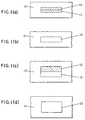
- a semiconductor substrate 10 containing a stable buried damaged region 12 and an amorphous region 14 which are formed in the surface of the semiconductor substrate using steps (a) and (b) of the present invention. These two steps as well as other aspects and embodiments of the present invention will now be described. It should be emphasized that the blanket structure shown in Fig. 1(a) can be employed as well as patterned SOI structures which may contain various mask materials such as dielectric cap layers and the like on the surface of the semiconductor substrate to define SOI regions. For clarity, the mask materials or dielectric cap layers that may be present on the surface of semiconductor substrate 10 are not shown in the drawings.
- Semiconductor substrate 10 that is employed in the present invention is composed of conventional semiconductor materials which are typically employed in forming SOI devices. Examples of such semiconductor materials include, but are not limited to, silicon (Si), germanium (Ge), Si/Ge alloys, gallium arsenide (GaAs), and other 4-4, 3-5, 2-6 binary or ternary compounds.
- a highly preferred semiconductor material for semiconductor substrate 10 is Si.
- the semiconductor substrate can be used as is, or it may be cleaned prior to use to remove any contaminants which may be present in or on the substrate. Any of the well known cleaning methods known to those skilled in the art may be employed in the present invention to remove said contaminants.
- semiconductor substrate 10 is irradiated with a first ion at a first dose; i.e. base dose, sufficient to implant said first ion into semiconductor substrate 10.
- a first dose i.e. base dose
- an ion is implanted into semiconductor substrate 10 by utilizing a SIMOX or other equivalent implanter.
- the ions that are implanted by this step are those which are capable of creating a stable defect region 12 in semiconductor substrate 10. Examples of such ions that can be employed in the present invention are oxygen, nitrogen, carbon, germanium, bismuth, antimony, phosphorus, arsenide and the like.
- a highly preferred first ion employed in the present invention is oxygen.
- the first ion is implanted utilizing a high temperature/low dose SIMOX ion implantation step. Accordingly, the first ion is implanted utilizing an ion implantation apparatus having a beam current of from about 5 to about 60 milliamps and that operates at an energy of from about 30 to about 400 keV. More preferably, the first ion is implanted at an energy of from about 170 to about 200 keV.
- the dosage, i.e. concentration, of the first ion implanted is from about 5x10 16 to about 6x10 17 cm -2 . More preferably, the dosage of the first ion is from about 2x10 17 to about 5x10 17 cm -2 .
- This first ion implantation step, or base ion implantation step is carried out at a temperature of from about 200° to about 700°C for a time period of from about 100 to about 200 minutes. More preferably, step (a) of the present invention is carried out at a temperature of from about 550° to about 575°C for a time period of from about 150 to about 180 minutes.
- the first ion used in forming damaged region 12 is implanted to a depth of from about 1000 to about 4000 ⁇ . More preferably, the first ion used in forming damaged region 12 is implanted to a depth of from about 3000 to about 4000 ⁇ .
- Adjacent amorphous region 14, which is connected to damaged region 12, is created by irradiating the surface of semiconductor substrate 10 containing damaged region 12 using a low temperature/low dose ion implantation step.
- the second implanted ion used in creating amorphous region 14 in semiconductor substrate 10 can be the same or different from the first ion used in creating damaged region 12.
- a highly preferred second ion used in forming amorphous region 14 is oxygen. It should be noted that although Fig. 1(a) depicts the adjacent amorphous region as being shallower than the damaged region, the present invention also contemplates that amorphous region 14 can be at the same or deeper depth than the damaged region.
- the implant energy used in forming amorphous region 14 is from about 50 to about 200 keV. More preferably, amorphous region 14 is formed by implanting said second ion using an energy of from about 170 to about 200 keV.
- the dose of the second ion used in forming amorphous region 14 is from about 1x10 14 to about 1x10 16 , more preferably, from about 3x10 14 to about 2x10 15 , cm -2 .
- step (b) of the present invention is conducted at much lower temperatures (less than 300°C).
- amorphous region 14 is formed by implanting a second ion at temperatures of from about -269° to about 300°C for a time period of from about 5 seconds to about 20 minutes.
- the low temperature/low dose ion implantation step is carried out at a temperature of from about 25° to about 150°C for a time period of from about 30 seconds to about 5 minutes.
- the second ion used in forming amorphous region 14 is implanted to a depth of from about 1000 to about 4000 ⁇ . More preferably, the second ion used in forming amorphous region 14 is implanted to a depth of from about 3000 to about 4000 ⁇ .
- the semiconductor material is then subjected to oxidation under conditions effective to cause diffusion of oxygen into semiconductor substrate 10. Under appropriate conditions, a continuous BOX region 16 is formed, as is shown in Fig. 1(b).
- An intermediate structure which comprises a thin layer of highly defective silicon 18 adjacent to and connected to BOX region 16 can also be created by modifying oxidation conditions, as shown in Fig. 1(c). Such structures are highly desirable in SOI based integrated circuits where floating body effects need to be minimized. Further steps, i.e., annealing, are typically required when this intermediate structure forms or when the dose of the base ion implant is less than 4x10 17 cm -2 .
- oxidation is carried out in an inert ambient that is mixed with oxygen.
- the inert ambient comprises an atmosphere of nitrogen, argon, helium or mixtures thereof that is mixed with about 5 to about 100 % oxygen.
- a highly preferred ambient utilized in the present invention during the oxidation step is argon (Ar) that is mixed with about 10 to about 40 % oxygen.
- the oxidation step is carried out at temperatures of from about 1300° to about 1375°C for a time period of from about 1 to about 24 hours. More preferably, the oxidation step of the present invention is carried out at a temperature of from about 1320° to about 1350°C for a time period of from about 5 to about 12 hours.
- the surface oxide that is formed may or may not be removed with HF prior to annealing.
- Fig. 1(c) When the intermediate structure shown in Fig. 1(c) is formed it is then annealed in an inert gas atmosphere, e.g. nitrogen, argon and the like, under conditions which are effective in improving the previously-formed buried oxide regions.
- the annealing step may also be carried out in an inert gas atmosphere that is mixed with from about 0.2 to about 5 % oxygen.
- Fig. 1(d) shows the after annealed product containing a new buried oxide region 20.
- Buried oxide region 20 is formed by annealing at a temperature of from about 1250° to about 1350°C for a time period of from about 1 to about 24 hours. More preferably, annealing is conducted at a temperature of from about 1320° to about 1350°C for a time period of from about 5 to about 15 hours.
- the present invention also contemplates combining these two processes into one heat cycle.
- the structure containing damage region 12 and amorphous region 14 is subjected to the following conditions: First, the structure is initially heated from room temperature to a temperature of from about 1300° to about 1375°C using a ramp-up rate of from about 2 to about 10°C/min. This initial heating is typically carried out in an inert gas atmosphere which can be mixed with oxygen. When oxygen is present in the initial heating step, it typically is present in an amount of from 0.1 to about 10 %. Various hold or so-called 'soak cycles' may be included in the initial heating step.
- a soak cycle When such a soak cycle is required, it typically occurs at about 1000°C for a time period of from about 5 to about 120 minutes. After said soak cycle, the structure is heated from 1000°C to the desired oxidation temperature (from about 1300° to about 1375°C) at a ramp-up rate of from about 1° to about 5°C/min.
- oxidation and annealing as described hereinabove are carried out followed by subsequent cooling to room temperature in an inert gas atmosphere which may contain 0.1 to 5 % oxygen at a cool-down rate of from about 0.1° to about 5°C/min.
- Various hold or soak cycles may be employed in the cool-down portion of the heating cycle.
- the DIBOX structures formed in the present invention can be used in forming high performance SOI devices or circuits.
- Examples of such devices or circuits that can contain the DIBOX of the present invention include microprocessors, memory cells such as DRAMs or SRAMs, ASICs and larger and more complicated circuits. Since these devices are well known to those skilled in the art, it is not necessary to provide a detailed description on how the same is fabricated.
- the BOX regions 16 or 20 formed by the method of the present invention generally have a thickness of from about 800 to about 2000 ⁇ . More preferably, the BOX thickness produced by the instant invention is from about 1000 to about 1500 ⁇ . It is possible to create any number of BOX regions within a semiconductor material having various thicknesses by simply repeating the steps of the present invention.
- the BOX region is not continuous for ion doses of 3x10 17 cm -2 or less. Moreover, pronounced surface roughness (>15 ⁇ Rms) is observed on such samples by atomic force microscopy. Such surface roughness is incompatible with modern high density integrated circuits.
- the implant and annealing sequence listed above i.e. base dose implantation and room temperature implantation in conjunction with oxidation and annealing, a highly continuous BOX structure is formed without causing any depreciable surface roughness which would limit the applicability of the sample.
- a continuous BOX region is formed directly after the oxidation step.
- the method of the present invention i.e. room temperature implantation and high temperature annealing, enhances the diffusion of oxygen into the silicon.
- the circles show how much buried oxide can be formed theoretically based on the ion dose.
- the squares in Fig. 2 show how much actual buried oxide is created by one embodiment of the method of the present invention.
- the difference of thickness at a given base dose gives the extra thermal buried oxide region created by the present invention.
- the method of the present invention not only improves the electrical and structural qualities of the BOX, but also saves implant time and SOI wafer cost.
- DIBOX regions were created using the method of the present invention. Specifically, DIBOX regions were created in three Si wafers using the following conditions and procedures:
- TEMs of each wafer were taken.
- a pictorial representation of one of the TEMs for one of the wafers is shown in Fig. 3.
- 10 represents a Si substrate
- 16 represents a BOX region
- 30 represent a SOI region formed by masking Si substrate 10.
- Wafer 1 a buried oxide region having a thickness of 1000 ⁇ was created by the method of the present invention.
- the BOX region had a thickness of 1100 ⁇ whereas the thickness of the BOX region in Wafer 3 was 1700 ⁇ .
- a method of fabricating a defect induced buried oxide region in a semiconductor material comprising (a) creating a stable buried damaged region in a semiconductor substrate, (b) forming an amorphous layer adjacent to said stable buried damaged region, and (c) oxidizing the structure produced by step (b), carrying out step (b) in a single step with a single temperature or multiple steps with multiple temperatures which range from about -269° to about 300°C.
- Step (c) is preferably carried out in an inert gas atmosphere that is mixed with from about 5 to about 100% oxygen, preferably in Ar mixed with about 10 to about 40% oxygen.
- Step (c) is preferably carried out at a temperature of from about 1300° to about 1375°C for a time period of from about 1 to about 24 hours, and more preferably at a temperature of from about 1320° to about 1350°C for a time period of from about 5 to about 15 hours.
- step (d) is preferably carried out in an inert gas atmosphere or a mixture of an inert gas and from about 10 to about 40 % oxygen at a temperature of from about 1250° to about 1350°C for a time period of from about 1 to about 24 hours, and more preferably step (d) is carried out at a temperature of from about 1320° to about 1350°C for a time period of from about 5 to about 15 hours.
- oxygen ions are preferably used in steps (a) and (b).
- a buried oxide region having a thickness of from about 800 to about 2000 ⁇ is preferably formed.
- the buried oxide region preferably has a thickness of from about 1000 to about 1500 ⁇ .
- Steps (c) and (d) are preferably combined into a single heating cycle.
- the single heating cycle preferably comprises the steps of:
- the semiconductor substrate may be patterned or unpatterned.
Abstract
Description
- The present invention relates to producing high throughput silicon on insulator (SOI) materials and, in particular, to a method of fabricating a defect induced buried oxide (DIBOX) region in a semiconductor substrate.
- In semiconductor manufacturing, several processes have been developed to produce a SOI device having a thin buried oxide (BOX) region disposed therein. One such process used in the prior art to produce BOX regions is referred to as SIMOX (separation by implantation of oxygen). In this process, the BOX region is fabricated by first implanting oxygen using high ion doses (>4x1017 cm-2) followed by annealing at high temperatures (>1300°C) Despite the current advances made in this field most of the prior art SIMOX processes produce a BOX region which is electrically inferior to thermally created oxide regions. Moreover, prior art SIMOX processes often times create a BOX region which contains silicon islands buried within the BOX. Typically, BOX regions produced using prior art SIMOX processes have discrete regions of thicknesses of about 1000 Å or 2000 Å. These thicknesses are determined by the implanted oxygen dose which is in the range of about 4-5x1017 cm-2 for the 1000 Å thick BOX and about 8-10x1017 cm-2 for the 2000 Å thick BOX. Thinner continuous BOX regions cannot be obtained using prior art SIMOX processes. Moreover, the prior art use of high ion doses to create a BOX region in a semiconductor substrate is not economical and is usually four to six times the bulk silicon cost. This high cost makes the use of prior art SOI materials undesirable.
- In view of the drawbacks mentioned hereinabove concerning prior SIMOX processes of fabricating a BOX region in a semiconductor material, there remains a need for providing a new and improved method of creating a BOX region in SOI materials. Specifically, it would be desirable to provide a new method wherein a continuous BOX region could be created in a semiconductor substrate having a wide range of thicknesses.
- The present invention provides a method of fabricating a semiconductor material containing a defect induced buried oxide (BOX) region therein, which mitigates some of all of the aforementioned problems with prior art SIMOX processes.
- The present invention according to a preferred embodiment provides a method which allows for the fabrication of a continuous BOX region using oxygen doses of about 3x1017 cm-2 or less.
- The invention according to a preferred embodiment provides a method which allows for the fabrication of a BOX region that exhibits high structural as well as electrical qualities.
- A preferred embodiment provides a BOX region in a SOI material which has a greater range of thickness than BOX regions prepared using conventional methods.
- The DIBOX region produced by the method of the present invention thus has improved structural and electrical qualities as compared with prior art BOX regions. Moreover, the method of the present invention produces BOX regions having a greater thickness than prior art methods. Hence, the method of the present invention saves implant time and ultimately SOI wafer cost.
- In one embodiment, the invention provides a method wherein a defect induced buried oxide region is formed in a semiconductor material using lower ion doses than heretofore reported in the prior art.
- Specifically, a first method according to the present invention comprises the steps of:
- (a) creating a stable buried damaged region in a semiconductor substrate;
- (b) forming an amorphous layer adjacent to said stable buried damaged region;
- (c) oxidizing the structure produced by step (b); and
- (d) optionally, annealing the oxidized structure provided in step (c).
-
- According to a preferred embodiment of the present invention, step (a) is carried out by implanting oxygen ions into a semiconductor substrate, which is either bear or contains a cap layer, e.g., a dielectric cap layer, using a low dose ion implantation step (on the order of 5x1016 cm-2 or greater) which is carried out at a high temperature of from about 200°C or higher.
- Step (b) of the present invention includes a yet lower ion dose implantation step using the same or different energy and ion as used in step (a). Step (b) of the present invention is carried out at about cryogenic temperatures to temperatures of about 300°C or less. The ion dosage used in this step of the present invention is generally of from about 2x10¹⁴ to about 4x1015 cm-2.
- This low temperature/low dose ion implantation step may be carried out in either a single step with a single temperature or multiple steps with multiple temperatures which range from about cryogenic to about 300°C or less.
- The oxidation step, step (c), is typically carried out in an inert ambient such as N2 or Ar mixed with oxygen at temperatures of from about 1300°C or higher. Under some circumstances, particularly when like ions are implanted in steps (a) and (b), this step causes the formation of a continuous BOX region.
- The optional step of the present invention is an anneal step which is normally carried out in an ambient containing a mixture of an inert gas and oxygen at temperatures of about 1300°C or higher for a period of time of about 5 to about 20 hours. The optional anneal step is carried when the foregoing oxidation step does not form a BOX region with desired structural and electrical properties. Normally, a BOX region is formed after oxidation when like ions, such as oxygen ions, are implanted in both steps (a) and (b).
- The term "high structural quality" is used herein to denote a structure which has little or no etch pit density (less than 1x105 cm2); little or no top or bottom Si/buried oxide roughness (less than 200 Å as observed by TEM spectroscopy); a low HF-defect density (less than 5 cm2); a low surface roughness (5 Å root mean square(Rms)); and, if present, the silicon precipitates in the buried oxide region at a low density (less than 1x105 cm2) and a small size (less than 500 Å in height). The structural quality can be determined using optical, atomic force scanning and/or transmission microscopy.
- The term "high electrical quality" is used herein to denote a structure wherein the BOX breakdown field is high (greater-than 5 megavolts per cm); the BOX minibreakdown voltage is high (greater than 30 volts); the BOX leakage at a given voltage is low (less than 1 nanoAmps); and the BOX defect density is low (less than 2 cm2).
- Another aspect of the present invention relates to a SOI material having a continuous BOX region formed in a semiconductor substrate by the method of the present invention. The BOX region formed by the instant invention has a variable, but controllable, continuous thickness which can typically range from about 800 to about 2000 Å by varying the first ion implanation step such that the base dose is from about 2x10¹⁷ to about 6x1017 cm-2. Such a controllable, continuous range of BOX thicknesses cannot be obtained utilizing prior art SIMOX processes.
-
- Figs. 1(a)-(d) are cross-sectional views of a semiconductor substrate after different processing steps of the present invention.
- Fig. 2 is a plot showing how the damage created by room temperature implantation enhances diffusion of oxygen in silicon during high temperature annealing and creates additional oxide in the ion implanted region.
- Fig. 3 is a representation of a TEM of one of the wafers treated as in Example 1.
-
- The present invention which provides a method of fabricating a DIBOX in a semiconductor substrate will now be described in more detail with reference to the accompanying drawings wherein like reference numerals are used for like and corresponding elements of the drawings.
- Referring first to Fig. 1(a), there is shown a
semiconductor substrate 10 containing a stable buried damagedregion 12 and anamorphous region 14 which are formed in the surface of the semiconductor substrate using steps (a) and (b) of the present invention. These two steps as well as other aspects and embodiments of the present invention will now be described. It should be emphasized that the blanket structure shown in Fig. 1(a) can be employed as well as patterned SOI structures which may contain various mask materials such as dielectric cap layers and the like on the surface of the semiconductor substrate to define SOI regions. For clarity, the mask materials or dielectric cap layers that may be present on the surface ofsemiconductor substrate 10 are not shown in the drawings. -
Semiconductor substrate 10 that is employed in the present invention is composed of conventional semiconductor materials which are typically employed in forming SOI devices. Examples of such semiconductor materials include, but are not limited to, silicon (Si), germanium (Ge), Si/Ge alloys, gallium arsenide (GaAs), and other 4-4, 3-5, 2-6 binary or ternary compounds. A highly preferred semiconductor material forsemiconductor substrate 10 is Si. - The semiconductor substrate can be used as is, or it may be cleaned prior to use to remove any contaminants which may be present in or on the substrate. Any of the well known cleaning methods known to those skilled in the art may be employed in the present invention to remove said contaminants.
- Next,
semiconductor substrate 10 is irradiated with a first ion at a first dose; i.e. base dose, sufficient to implant said first ion intosemiconductor substrate 10. In accordance with this step of the present invention, an ion is implanted intosemiconductor substrate 10 by utilizing a SIMOX or other equivalent implanter. The ions that are implanted by this step are those which are capable of creating astable defect region 12 insemiconductor substrate 10. Examples of such ions that can be employed in the present invention are oxygen, nitrogen, carbon, germanium, bismuth, antimony, phosphorus, arsenide and the like. A highly preferred first ion employed in the present invention is oxygen. - As stated above, the first ion is implanted utilizing a high temperature/low dose SIMOX ion implantation step. Accordingly, the first ion is implanted utilizing an ion implantation apparatus having a beam current of from about 5 to about 60 milliamps and that operates at an energy of from about 30 to about 400 keV. More preferably, the first ion is implanted at an energy of from about 170 to about 200 keV. The dosage, i.e. concentration, of the first ion implanted is from about 5x10¹⁶ to about 6x1017 cm-2. More preferably, the dosage of the first ion is from about 2x10¹⁷ to about 5x1017 cm-2.
- This first ion implantation step, or base ion implantation step, is carried out at a temperature of from about 200° to about 700°C for a time period of from about 100 to about 200 minutes. More preferably, step (a) of the present invention is carried out at a temperature of from about 550° to about 575°C for a time period of from about 150 to about 180 minutes.
- Using the above defined parameters, the first ion used in forming damaged
region 12 is implanted to a depth of from about 1000 to about 4000 Å. More preferably, the first ion used in forming damagedregion 12 is implanted to a depth of from about 3000 to about 4000 Å. - Adjacent
amorphous region 14, which is connected to damagedregion 12, is created by irradiating the surface ofsemiconductor substrate 10 containing damagedregion 12 using a low temperature/low dose ion implantation step. The second implanted ion used in creatingamorphous region 14 insemiconductor substrate 10 can be the same or different from the first ion used in creating damagedregion 12. A highly preferred second ion used in formingamorphous region 14 is oxygen. It should be noted that although Fig. 1(a) depicts the adjacent amorphous region as being shallower than the damaged region, the present invention also contemplates thatamorphous region 14 can be at the same or deeper depth than the damaged region. - The implant energy used in forming
amorphous region 14 is from about 50 to about 200 keV. More preferably,amorphous region 14 is formed by implanting said second ion using an energy of from about 170 to about 200 keV. The dose of the second ion used in formingamorphous region 14 is from about 1x10¹⁴ to about 1x10¹⁶, more preferably, from about 3x10¹⁴ to about 2x10¹⁵, cm-2. - Unlike the first step of the present invention, which is conducted at high temperatures, step (b) of the present invention is conducted at much lower temperatures (less than 300°C). Specifically,
amorphous region 14 is formed by implanting a second ion at temperatures of from about -269° to about 300°C for a time period of from about 5 seconds to about 20 minutes. More preferably, the low temperature/low dose ion implantation step is carried out at a temperature of from about 25° to about 150°C for a time period of from about 30 seconds to about 5 minutes. - Using the above defined conditions, the second ion used in forming
amorphous region 14 is implanted to a depth of from about 1000 to about 4000 Å. More preferably, the second ion used in formingamorphous region 14 is implanted to a depth of from about 3000 to about 4000 Å. - After creating damaged
region 12 andamorphous region 14 insemiconductor substrate 10, the semiconductor material is then subjected to oxidation under conditions effective to cause diffusion of oxygen intosemiconductor substrate 10. Under appropriate conditions, acontinuous BOX region 16 is formed, as is shown in Fig. 1(b). - An intermediate structure which comprises a thin layer of highly
defective silicon 18 adjacent to and connected to BOXregion 16 can also be created by modifying oxidation conditions, as shown in Fig. 1(c). Such structures are highly desirable in SOI based integrated circuits where floating body effects need to be minimized. Further steps, i.e., annealing, are typically required when this intermediate structure forms or when the dose of the base ion implant is less than 4x1017 cm-2. - In accordance with the present invention, oxidation is carried out in an inert ambient that is mixed with oxygen. Typically, the inert ambient comprises an atmosphere of nitrogen, argon, helium or mixtures thereof that is mixed with about 5 to about 100 % oxygen. A highly preferred ambient utilized in the present invention during the oxidation step is argon (Ar) that is mixed with about 10 to about 40 % oxygen.
- The oxidation step is carried out at temperatures of from about 1300° to about 1375°C for a time period of from about 1 to about 24 hours. More preferably, the oxidation step of the present invention is carried out at a temperature of from about 1320° to about 1350°C for a time period of from about 5 to about 12 hours. Following the oxidation step, the surface oxide that is formed may or may not be removed with HF prior to annealing.
- When the intermediate structure shown in Fig. 1(c) is formed it is then annealed in an inert gas atmosphere, e.g. nitrogen, argon and the like, under conditions which are effective in improving the previously-formed buried oxide regions. The annealing step may also be carried out in an inert gas atmosphere that is mixed with from about 0.2 to about 5 % oxygen. Fig. 1(d) shows the after annealed product containing a new buried
oxide region 20.Buried oxide region 20 is formed by annealing at a temperature of from about 1250° to about 1350°C for a time period of from about 1 to about 24 hours. More preferably, annealing is conducted at a temperature of from about 1320° to about 1350°C for a time period of from about 5 to about 15 hours. - In addition to separate oxidation and annealing steps, the present invention also contemplates combining these two processes into one heat cycle. When this embodiment of the present invention is carried out, the structure containing
damage region 12 andamorphous region 14 is subjected to the following conditions: First, the structure is initially heated from room temperature to a temperature of from about 1300° to about 1375°C using a ramp-up rate of from about 2 to about 10°C/min. This initial heating is typically carried out in an inert gas atmosphere which can be mixed with oxygen. When oxygen is present in the initial heating step, it typically is present in an amount of from 0.1 to about 10 %. Various hold or so-called 'soak cycles' may be included in the initial heating step. When such a soak cycle is required, it typically occurs at about 1000°C for a time period of from about 5 to about 120 minutes. After said soak cycle, the structure is heated from 1000°C to the desired oxidation temperature (from about 1300° to about 1375°C) at a ramp-up rate of from about 1° to about 5°C/min. - Thereafter, oxidation and annealing as described hereinabove are carried out followed by subsequent cooling to room temperature in an inert gas atmosphere which may contain 0.1 to 5 % oxygen at a cool-down rate of from about 0.1° to about 5°C/min. Various hold or soak cycles may be employed in the cool-down portion of the heating cycle. Also, it is contemplated to change the rate of cooling during the cooling cycle. For example, at a temperature of from about 900° to about 1100°C, the cooling rate may be changed to about 0.1° to about 10°C/min until a temperature reading of from about 600° to about 800°C is obtained. Thereafter, the cooling rate may be switched to another rate within the range of from 3° to about 10°C/min.
- It is noted that during the above described annealing step, which is carried out under a high oxygen content, two adjacent stable buried regions are created. Specifically, a highly defective region consisting of primarily Si polycrystals, microtwins and stacking faults form in the amorphous region. This defect-containing layer is believed to enhance oxygen diffusion into silicon and combines with the first created damaged layer during this annealing step to form the buried oxide region in the semiconductor substrate.
- The DIBOX structures formed in the present invention can be used in forming high performance SOI devices or circuits. Examples of such devices or circuits that can contain the DIBOX of the present invention include microprocessors, memory cells such as DRAMs or SRAMs, ASICs and larger and more complicated circuits. Since these devices are well known to those skilled in the art, it is not necessary to provide a detailed description on how the same is fabricated.
- The
BOX regions - It is noted that, if the amorphous region is not formed by the second implant, the BOX region is not continuous for ion doses of 3x1017 cm-2 or less. Moreover, pronounced surface roughness (>15 Å Rms) is observed on such samples by atomic force microscopy. Such surface roughness is incompatible with modern high density integrated circuits. In contrast, by employing the implant and annealing sequence listed above, i.e. base dose implantation and room temperature implantation in conjunction with oxidation and annealing, a highly continuous BOX structure is formed without causing any depreciable surface roughness which would limit the applicability of the sample. In the case where oxygen is implanted in steps (a) and (b), a continuous BOX region is formed directly after the oxidation step.
- Also, as is shown in Fig. 2, the method of the present invention, i.e. room temperature implantation and high temperature annealing, enhances the diffusion of oxygen into the silicon. Specifically, in Fig. 2 the circles show how much buried oxide can be formed theoretically based on the ion dose. The squares in Fig. 2 show how much actual buried oxide is created by one embodiment of the method of the present invention. The difference of thickness at a given base dose gives the extra thermal buried oxide region created by the present invention. Thus, the method of the present invention, not only improves the electrical and structural qualities of the BOX, but also saves implant time and SOI wafer cost.
- The following examples are given to illustrate the scope of the present invention. Because these examples are given for illustrative purpose only, the invention embodied thereon should not be limited thereto.
- In this example, various DIBOX regions were created using the method of the present invention. Specifically, DIBOX regions were created in three Si wafers using the following conditions and procedures:
-
- (a) base implant ion O+; implant energy 185 keV; implant dose 2x1017 cm-2; implant temperature 570°C, beam current 50-55 mA;
- (b) room temperature implant ion O+; implant energy 185 keV; implant temperature room temperature; beam current 10-30 mA;
- (c) oxidation: ramp-up from 200°C to 1000°C, 4.5°C/min, ambient Ar and 2 % O2; Soak at 1000°C, 30 min, ambient 100% O2; ramp-up from 1000° to 1320°C: 2.6°C/min, ambient 60% Ar and 40% O2; hold 12 hours;
- (d) anneal continue from (c): temperature 1320°C, hold 10 hrs, ambient Ar and 2.25% O2; ramp-down to 1000°C at 1°C/min; ramp-down from 1000°C to 800°C at 3°C/min; ramp-down from 800°C to 200°C at 4.5°C/min.
-
-
- (a) base implant ion O+; implant energy 200 keV; implant dose 3x1017 cm-2; implant temperature 570°C; beam current 50-55 mA;
- (b) room temperature implant ion O+; implant energy 200 keV; implant temperature room temperature; beam current 10-30 mA;
- (c) oxidation: ramp-up from 200°C to 1000°C, 4.5°C/min, ambient Ar and 2% O2; soak at 1000°C, 30 min, ambient 100% O2; ramp-up from 1000°C to 1320°C, 2.6°C/min, ambient 75% Ar and 25% O2; hold 12 hrs;
- (d) anneal continued from (c); temperature 1320°C, hold 10 hrs, ambient Ar and 2.25% O2; ramp-down to 1000°C at 1°C/min; ramp-down from 1000°C to 800°C at 3°C/min; ramp-down from 800°C to 200°C at 4.5°C/min.
-
-
- (a) base implant ion O+; implant energy 185 keV; implant dose 4.5x1017 cm-2; implant temperature 570°C; beam current 50-55 mA;
- (b) room temperature implant ion O+; implant energy 185 keV; implant temperature room temperature; beam current 10-30 mA;
- (c) oxidation: ramp-up from 200°C to 1000°C, 4.5°C/min, ambient Ar and 2% O2; soak at 1000°C, 30 min., ambient 100% O2; ramp-up from 1000°C, 30 min., ambient 100%; ramp-up from 1000°C to 1320°C, 2.6°C/min, ambient 60% Ar and 40% O2; hold 12 hrs.
- (d) anneal continue from (c); temperature 1320°C, hold 10 hrs., ambient Ar and 2.25% O2; ramp-down to 1000°C at 1°C/min; ramp-down from 1000°C to 800°C at 3°/min; ramp-down from 800°C to 200°C at 4.5°C/min.
-
- After conducting the above steps, TEMs of each wafer were taken. A pictorial representation of one of the TEMs for one of the wafers is shown in Fig. 3. In Fig. 3, 10 represents a Si substrate, 16 represents a BOX region; and 30 represent a SOI region formed by masking
Si substrate 10. - In regard to Wafer 1, a buried oxide region having a thickness of 1000 Å was created by the method of the present invention. In
Wafer 2, the BOX region had a thickness of 1100 Å whereas the thickness of the BOX region in Wafer 3 was 1700 Å. - The above example clearly shows that the method of the present invention is capable of producing BOX regions having various thicknesses.
- Additional preferred features of a method according to the inventions are as follows:
- In a method of fabricating a defect induced buried oxide region in a semiconductor material comprising (a) creating a stable buried damaged region in a semiconductor substrate, (b) forming an amorphous layer adjacent to said stable buried damaged region, and (c) oxidizing the structure produced by step (b), carrying out step (b) in a single step with a single temperature or multiple steps with multiple temperatures which range from about -269° to about 300°C.
- Step (c) is preferably carried out in an inert gas atmosphere that is mixed with from about 5 to about 100% oxygen, preferably in Ar mixed with about 10 to about 40% oxygen.
- Step (c) is preferably carried out at a temperature of from about 1300° to about 1375°C for a time period of from about 1 to about 24 hours, and more preferably at a temperature of from about 1320° to about 1350°C for a time period of from about 5 to about 15 hours.
- In a method of fabricating a defect induced buried oxide region in a semiconductor material, step (d) is preferably carried out in an inert gas atmosphere or a mixture of an inert gas and from about 10 to about 40 % oxygen at a temperature of from about 1250° to about 1350°C for a time period of from about 1 to about 24 hours, and more preferably step (d) is carried out at a temperature of from about 1320° to about 1350°C for a time period of from about 5 to about 15 hours.
- In the method of the invention, oxygen ions are preferably used in steps (a) and (b).
- A buried oxide region having a thickness of from about 800 to about 2000 Å is preferably formed. In particular, the buried oxide region preferably has a thickness of from about 1000 to about 1500 Å.
- Steps (c) and (d) are preferably combined into a single heating cycle. The single heating cycle preferably comprises the steps of:
- (a) heating the structure from room temperature to a temperature within the range of from about 1300° to about 1375°C at a ramp-up rate of from about 3° to about 10°C/min;
- (b) oxidizing said structure at a temperature of from about 1300° to about 1375°C for a time period of from about 1 to 24 hours;
- (c) annealing said structure at a temperature of from about 1250° to about 1350°C for a time period of from about 1 to 24 hours; and
- (d) cooling said structure from said annealing temperature to room temperature at a rate of from about 0.10 to about 5°C/minute.
-
- The semiconductor substrate may be patterned or unpatterned.
- While the instant invention has been particularly shown and described with respect to preferred embodiments thereof, it will be apparent to those skilled in the art than the foregoing and other changes in form and detail may be made without departing from the spirit and scope of the present invention.
Claims (20)
- A method of fabricating a defect induced buried oxide region in a semiconductor material comprising:(a) creating a stable buried damaged region in a semiconductor substrate;(b) forming an amorphous layer adjacent to said stable buried damaged region; and(c) oxidizing the structure produced by step (b).
- The method of claim 1 further comprising (d) annealing the oxidized structure provided in step (c).
- The method of claim 1 or claim 2 wherein said semiconductor substrate is composed of a semiconductor material selected from the group consisting of silicon, gallium, Si/Ge alloys, GaAs, and other 4-4, 3-5 or 2-6 binary or ternary compounds.
- The method of any one of claims 1 to 3 wherein said semiconductor substrate is bear or contains at least one dielectric cap layer.
- The method of any preceding claim, wherein step (a) comprises irradiating a surface of said semiconductor substrate with a first ion using an energy of from about 30 to about 400 keV and at a temperature of from about 200° to about 700°C for a time period of from about 100 to about 200 minutes.
- The method of claim 5 wherein said first ion is implanted at an energy of from about 170 to about 200 keV and at a temperature of from about 550° to about 575°C for a time period of from about 150 to about 180 minutes.
- The method of claim 5 wherein said first ion is selected front the group consisting of oxygen, nitrogen, carbon, germanium, bismuth, antimony, phosphorus and arsenide.
- The method of claim 5 wherein said first ion is implanted at a dose of from about 5x10¹⁶ to about 6x1017 cm-2.
- The method of claim 8 wherein the first ion dose is from about 2x10¹⁷ to about 5x1017 cm-2.
- The method of claim 5 wherein the first ion is implanted to a depth of from about 1000 to about 4000 Å.
- The method of claim 10 wherein the first ion is implanted to a depth of from about 3000 to about 4000 Å.
- The method of any preceding claim wherein step (b) is carried out by irradiating said surface of said semiconductor substrate with a second ion using an energy of from about 50 to about 200 keV, and at a temperature of from about -269° to about 300°C for a time period of from about 5 seconds to about 20 minutes.
- The method of claim 12 wherein said second ion is implanted at an energy of from about 170 to about 200 keV and at a temperature of from about 25° to about 200°C for a time period of from about 30 seconds to about 5 minutes.
- The method of claim 12 wherein said second ion is selected from the group consisting of oxygen, nitrogen, carbon, germanium, bismuth, antimony, phosphorus and arsenide.
- The method of claim 12 wherein said second ion is implanted at a dose of from about 1x10¹⁴ to about 1x1016 cm-2.
- The method of claim 15 wherein the second ion dose is from about 3x10¹⁴ to about 2x1015 cm-2.
- The method of claim 12 wherein the second ion is implanted to a depth of from about 1000 to about 4000 Å.
- The method of claim 16 wherein the second ion is implanted to a depth of from about 3000 to about 4000 Å.
- A silicon-on-insulator material comprising a semiconductor substrate having a continuous buried oxide region formed therein by the method of claim 1.
- A silicon-on-insulator material comprising a semiconductor substrate having a continuous buried oxide region formed therein by the method of claim 2.
Applications Claiming Priority (2)
| Application Number | Priority Date | Filing Date | Title |
|---|---|---|---|
| US08/995,585 US5930643A (en) | 1997-12-22 | 1997-12-22 | Defect induced buried oxide (DIBOX) for throughput SOI |
| US995585 | 1997-12-22 |
Publications (2)
| Publication Number | Publication Date |
|---|---|
| EP0926725A2 true EP0926725A2 (en) | 1999-06-30 |
| EP0926725A3 EP0926725A3 (en) | 2000-08-30 |
Family
ID=25541967
Family Applications (1)
| Application Number | Title | Priority Date | Filing Date |
|---|---|---|---|
| EP98310584A Ceased EP0926725A3 (en) | 1997-12-22 | 1998-12-22 | Defect induced buried oxide (dibox) for throughput SOI |
Country Status (5)
| Country | Link |
|---|---|
| US (2) | US5930643A (en) |
| EP (1) | EP0926725A3 (en) |
| KR (1) | KR100314420B1 (en) |
| CN (1) | CN1179408C (en) |
| TW (1) | TW432498B (en) |
Cited By (7)
| Publication number | Priority date | Publication date | Assignee | Title |
|---|---|---|---|---|
| WO2001084601A2 (en) * | 2000-05-03 | 2001-11-08 | Ibis Technology, Inc. | Implantation process using sub-stoichiometric, oxygen doses at different energies |
| WO2002045132A2 (en) * | 2000-11-28 | 2002-06-06 | Ibis Technology Corporation | Low defect density, thin-layer, soi substrates |
| WO2003041160A2 (en) * | 2001-11-05 | 2003-05-15 | Ibis Technology Corporation | Two-step ion implantation method with active wafer cooling for buried oxide formation |
| EP1460683A1 (en) * | 2001-12-26 | 2004-09-22 | Komatsu Denshi Kinzoku Kabushiki Kaisha | Method for vanishing defects in single crystal silicon and single crystal silicon |
| EP1744357A2 (en) | 2005-06-23 | 2007-01-17 | Sumco Corporation | Method for manufacturing SIMOX wafer and SIMOX wafer |
| EP1852908A1 (en) * | 2000-05-03 | 2007-11-07 | Ibis Technology, Inc. | Implantation process using sub-stoichiometric, oxygen doses at diferent energies |
| EP1914799A1 (en) * | 2005-07-29 | 2008-04-23 | Shanghai Simgui Technology Co., Ltd | Method for manufacturing silicon on insulator |
Families Citing this family (57)
| Publication number | Priority date | Publication date | Assignee | Title |
|---|---|---|---|---|
| US6486037B2 (en) * | 1997-12-22 | 2002-11-26 | International Business Machines Corporation | Control of buried oxide quality in low dose SIMOX |
| US6617034B1 (en) * | 1998-02-02 | 2003-09-09 | Nippon Steel Corporation | SOI substrate and method for production thereof |
| FR2777115B1 (en) * | 1998-04-07 | 2001-07-13 | Commissariat Energie Atomique | PROCESS FOR TREATING SEMICONDUCTOR SUBSTRATES AND STRUCTURES OBTAINED BY THIS PROCESS |
| JP4223092B2 (en) * | 1998-05-19 | 2009-02-12 | 株式会社半導体エネルギー研究所 | Method for manufacturing semiconductor device |
| US6228720B1 (en) * | 1999-02-23 | 2001-05-08 | Matsushita Electric Industrial Co., Ltd. | Method for making insulated-gate semiconductor element |
| JP2000243958A (en) * | 1999-02-24 | 2000-09-08 | Toshiba Corp | Semiconductor device and manufacture thereof |
| US6333532B1 (en) | 1999-07-16 | 2001-12-25 | International Business Machines Corporation | Patterned SOI regions in semiconductor chips |
| US6633066B1 (en) * | 2000-01-07 | 2003-10-14 | Samsung Electronics Co., Ltd. | CMOS integrated circuit devices and substrates having unstrained silicon active layers |
| JP2001297989A (en) * | 2000-04-14 | 2001-10-26 | Mitsubishi Electric Corp | Semiconductor substrate and manufacturing method thereof and semiconductor device and manufacturing method thereof |
| JP2002110688A (en) * | 2000-09-29 | 2002-04-12 | Canon Inc | Thermal processing method of soi, and its manufacturing method |
| JP2002231651A (en) * | 2001-02-02 | 2002-08-16 | Nippon Steel Corp | Simox substrate and its manufacturing method |
| KR100366923B1 (en) * | 2001-02-19 | 2003-01-06 | 삼성전자 주식회사 | SOI Substrate and Method of Manufacturing Thereof |
| US6541356B2 (en) | 2001-05-21 | 2003-04-01 | International Business Machines Corporation | Ultimate SIMOX |
| US6855436B2 (en) * | 2003-05-30 | 2005-02-15 | International Business Machines Corporation | Formation of silicon-germanium-on-insulator (SGOI) by an integral high temperature SIMOX-Ge interdiffusion anneal |
| US6602757B2 (en) | 2001-05-21 | 2003-08-05 | International Business Machines Corporation | Self-adjusting thickness uniformity in SOI by high-temperature oxidation of SIMOX and bonded SOI |
| US6846727B2 (en) | 2001-05-21 | 2005-01-25 | International Business Machines Corporation | Patterned SOI by oxygen implantation and annealing |
| US6596570B2 (en) * | 2001-06-06 | 2003-07-22 | International Business Machines Corporation | SOI device with reduced junction capacitance |
| US20020190318A1 (en) | 2001-06-19 | 2002-12-19 | International Business Machines Corporation | Divot reduction in SIMOX layers |
| US6531375B1 (en) | 2001-09-18 | 2003-03-11 | International Business Machines Corporation | Method of forming a body contact using BOX modification |
| US6531411B1 (en) | 2001-11-05 | 2003-03-11 | International Business Machines Corporation | Surface roughness improvement of SIMOX substrates by controlling orientation of angle of starting material |
| US6812114B2 (en) * | 2002-04-10 | 2004-11-02 | International Business Machines Corporation | Patterned SOI by formation and annihilation of buried oxide regions during processing |
| US6784072B2 (en) * | 2002-07-22 | 2004-08-31 | International Business Machines Corporation | Control of buried oxide in SIMOX |
| KR100743821B1 (en) * | 2003-02-25 | 2007-07-30 | 가부시키가이샤 섬코 | Method for growing silicon single crystal, method for manufacturing silicon wafer, and method for manufacturing soi substrate |
| US6964897B2 (en) * | 2003-06-09 | 2005-11-15 | International Business Machines Corporation | SOI trench capacitor cell incorporating a low-leakage floating body array transistor |
| DE10326578B4 (en) * | 2003-06-12 | 2006-01-19 | Siltronic Ag | Process for producing an SOI disk |
| US7169226B2 (en) * | 2003-07-01 | 2007-01-30 | International Business Machines Corporation | Defect reduction by oxidation of silicon |
| US7566482B2 (en) * | 2003-09-30 | 2009-07-28 | International Business Machines Corporation | SOI by oxidation of porous silicon |
| US7718231B2 (en) * | 2003-09-30 | 2010-05-18 | International Business Machines Corporation | Thin buried oxides by low-dose oxygen implantation into modified silicon |
| CN100461367C (en) * | 2004-01-09 | 2009-02-11 | 国际商业机器公司 | Formation of patterned silicon-on-insulator (soi)/silicon-on-nothing (son) composite structure by porous Si engineering |
| US20050170570A1 (en) * | 2004-01-30 | 2005-08-04 | International Business Machines Corporation | High electrical quality buried oxide in simox |
| US7172930B2 (en) * | 2004-07-02 | 2007-02-06 | International Business Machines Corporation | Strained silicon-on-insulator by anodization of a buried p+ silicon germanium layer |
| JP2006032785A (en) * | 2004-07-20 | 2006-02-02 | Sumco Corp | Method for manufacturing soi substrate and soi substrate |
| US7115463B2 (en) * | 2004-08-20 | 2006-10-03 | International Business Machines Corporation | Patterning SOI with silicon mask to create box at different depths |
| JP3998677B2 (en) * | 2004-10-19 | 2007-10-31 | 株式会社東芝 | Manufacturing method of semiconductor wafer |
| WO2006082469A1 (en) * | 2005-02-03 | 2006-08-10 | S.O.I.Tec Silicon On Insulator Technologies | Method for applying a high temperature treatment to a semimiconductor wafer |
| US20060228492A1 (en) * | 2005-04-07 | 2006-10-12 | Sumco Corporation | Method for manufacturing SIMOX wafer |
| JP4876442B2 (en) * | 2005-06-13 | 2012-02-15 | 株式会社Sumco | SIMOX wafer manufacturing method and SIMOX wafer |
| JP2007208023A (en) * | 2006-02-02 | 2007-08-16 | Sumco Corp | Manufacturing method of simox wafer |
| JP2007227424A (en) * | 2006-02-21 | 2007-09-06 | Sumco Corp | Production process of simox wafer |
| JP5157075B2 (en) * | 2006-03-27 | 2013-03-06 | 株式会社Sumco | SIMOX wafer manufacturing method |
| JP2007266059A (en) * | 2006-03-27 | 2007-10-11 | Sumco Corp | Method of manufacturing simox wafer |
| JP5061489B2 (en) * | 2006-04-05 | 2012-10-31 | 株式会社Sumco | SIMOX wafer manufacturing method |
| JP2008244261A (en) * | 2007-03-28 | 2008-10-09 | Shin Etsu Handotai Co Ltd | Manufacturing method of soi substrate |
| JP2009054837A (en) * | 2007-08-28 | 2009-03-12 | Sumco Corp | Simox wafer manufacturing method and simox wafer |
| US7955950B2 (en) * | 2007-10-18 | 2011-06-07 | International Business Machines Corporation | Semiconductor-on-insulator substrate with a diffusion barrier |
| JP5151651B2 (en) * | 2008-04-22 | 2013-02-27 | 株式会社Sumco | Oxygen ion implanter |
| JP2010003647A (en) * | 2008-06-23 | 2010-01-07 | Sumco Corp | Ion implantation device |
| JP2010015774A (en) * | 2008-07-02 | 2010-01-21 | Sumco Corp | Ion implantation apparatus |
| JP2010021041A (en) * | 2008-07-11 | 2010-01-28 | Sumco Corp | Wafer holder of ion implantation device |
| JP2010027959A (en) * | 2008-07-23 | 2010-02-04 | Sumco Corp | Method for manufacturing high-resistance simox wafer |
| JP2010062452A (en) * | 2008-09-05 | 2010-03-18 | Sumco Corp | Method of manufacturing semiconductor substrate |
| JP5766901B2 (en) * | 2008-11-28 | 2015-08-19 | 株式会社Sumco | Manufacturing method of bonded wafer |
| JP2010199569A (en) * | 2009-02-02 | 2010-09-09 | Sumco Corp | Method of manufacturing simox wafer |
| US20100216295A1 (en) * | 2009-02-24 | 2010-08-26 | Alex Usenko | Semiconductor on insulator made using improved defect healing process |
| US20130012008A1 (en) * | 2010-03-26 | 2013-01-10 | Bong-Gyun Ko | Method of producing soi wafer |
| US9059245B2 (en) | 2012-05-30 | 2015-06-16 | International Business Machines Corporation | Semiconductor-on-insulator (SOI) substrates with ultra-thin SOI layers and buried oxides |
| CN106548937B (en) * | 2015-09-18 | 2019-06-25 | 上海先进半导体制造股份有限公司 | The process of annealing |
Citations (7)
| Publication number | Priority date | Publication date | Assignee | Title |
|---|---|---|---|---|
| US4749660A (en) * | 1986-11-26 | 1988-06-07 | American Telephone And Telegraph Company, At&T Bell Laboratories | Method of making an article comprising a buried SiO2 layer |
| JPS63217657A (en) * | 1987-03-05 | 1988-09-09 | Nec Corp | Manufacture of semiconductor substrate |
| US4786608A (en) * | 1986-12-30 | 1988-11-22 | Harris Corp. | Technique for forming electric field shielding layer in oxygen-implanted silicon substrate |
| US4975126A (en) * | 1987-06-15 | 1990-12-04 | Commissariat A L'energie Atomique | Process for the production of an insulating layer embedded in a semiconductor substrate by ionic implantation and semiconductor structure comprising such layer |
| US5288650A (en) * | 1991-01-25 | 1994-02-22 | Ibis Technology Corporation | Prenucleation process for simox device fabrication |
| US5589407A (en) * | 1995-09-06 | 1996-12-31 | Implanted Material Technology, Inc. | Method of treating silicon to obtain thin, buried insulating layer |
| US6043166A (en) * | 1996-12-03 | 2000-03-28 | International Business Machines Corporation | Silicon-on-insulator substrates using low dose implantation |
Family Cites Families (3)
| Publication number | Priority date | Publication date | Assignee | Title |
|---|---|---|---|---|
| US4902642A (en) * | 1987-08-07 | 1990-02-20 | Texas Instruments, Incorporated | Epitaxial process for silicon on insulator structure |
| US5212397A (en) * | 1990-08-13 | 1993-05-18 | Motorola, Inc. | BiCMOS device having an SOI substrate and process for making the same |
| US5519336A (en) * | 1992-03-03 | 1996-05-21 | Honeywell Inc. | Method for electrically characterizing the insulator in SOI devices |
-
1997
- 1997-12-22 US US08/995,585 patent/US5930643A/en not_active Expired - Fee Related
-
1998
- 1998-11-23 KR KR1019980050150A patent/KR100314420B1/en not_active IP Right Cessation
- 1998-11-27 CN CNB981229417A patent/CN1179408C/en not_active Expired - Fee Related
- 1998-12-19 TW TW087121280A patent/TW432498B/en not_active IP Right Cessation
- 1998-12-22 EP EP98310584A patent/EP0926725A3/en not_active Ceased
-
1999
- 1999-03-09 US US09/264,973 patent/US6259137B1/en not_active Expired - Fee Related
Patent Citations (7)
| Publication number | Priority date | Publication date | Assignee | Title |
|---|---|---|---|---|
| US4749660A (en) * | 1986-11-26 | 1988-06-07 | American Telephone And Telegraph Company, At&T Bell Laboratories | Method of making an article comprising a buried SiO2 layer |
| US4786608A (en) * | 1986-12-30 | 1988-11-22 | Harris Corp. | Technique for forming electric field shielding layer in oxygen-implanted silicon substrate |
| JPS63217657A (en) * | 1987-03-05 | 1988-09-09 | Nec Corp | Manufacture of semiconductor substrate |
| US4975126A (en) * | 1987-06-15 | 1990-12-04 | Commissariat A L'energie Atomique | Process for the production of an insulating layer embedded in a semiconductor substrate by ionic implantation and semiconductor structure comprising such layer |
| US5288650A (en) * | 1991-01-25 | 1994-02-22 | Ibis Technology Corporation | Prenucleation process for simox device fabrication |
| US5589407A (en) * | 1995-09-06 | 1996-12-31 | Implanted Material Technology, Inc. | Method of treating silicon to obtain thin, buried insulating layer |
| US6043166A (en) * | 1996-12-03 | 2000-03-28 | International Business Machines Corporation | Silicon-on-insulator substrates using low dose implantation |
Non-Patent Citations (2)
| Title |
|---|
| PATENT ABSTRACTS OF JAPAN vol. 013, no. 005 (E-701), 9 January 1989 (1989-01-09) & JP 63 217657 A (NEC CORP), 9 September 1988 (1988-09-09) * |
| WHITE A E ET AL: "The role of implant temperature in the formation of thin buried oxide layers" BEAM-SOLID INTERACTIONS AND TRANSIENT PROCESSES SYMPOSIUM, BOSTON, MA, USA, 1-4 DEC. 1986, pages 585-590, XP000922701 1987, Pittsburgh, PA, USA, Mater. Res. Soc, USA ISBN: 0-931837-40-5 * |
Cited By (17)
| Publication number | Priority date | Publication date | Assignee | Title |
|---|---|---|---|---|
| WO2001084601A2 (en) * | 2000-05-03 | 2001-11-08 | Ibis Technology, Inc. | Implantation process using sub-stoichiometric, oxygen doses at different energies |
| WO2001084601A3 (en) * | 2000-05-03 | 2002-05-23 | Ibis Technology Inc | Implantation process using sub-stoichiometric, oxygen doses at different energies |
| EP1852908A1 (en) * | 2000-05-03 | 2007-11-07 | Ibis Technology, Inc. | Implantation process using sub-stoichiometric, oxygen doses at diferent energies |
| US6417078B1 (en) | 2000-05-03 | 2002-07-09 | Ibis Technology Corporation | Implantation process using sub-stoichiometric, oxygen doses at different energies |
| WO2002045132A3 (en) * | 2000-11-28 | 2003-02-13 | Ibis Technology Corp | Low defect density, thin-layer, soi substrates |
| US6593173B1 (en) | 2000-11-28 | 2003-07-15 | Ibis Technology Corporation | Low defect density, thin-layer, SOI substrates |
| WO2002045132A2 (en) * | 2000-11-28 | 2002-06-06 | Ibis Technology Corporation | Low defect density, thin-layer, soi substrates |
| WO2003041160A2 (en) * | 2001-11-05 | 2003-05-15 | Ibis Technology Corporation | Two-step ion implantation method with active wafer cooling for buried oxide formation |
| WO2003041160A3 (en) * | 2001-11-05 | 2004-03-11 | Ibis Technology Corp | Two-step ion implantation method with active wafer cooling for buried oxide formation |
| US6998353B2 (en) | 2001-11-05 | 2006-02-14 | Ibis Technology Corporation | Active wafer cooling during damage engineering implant to enhance buried oxide formation in SIMOX wafers |
| EP1460683A1 (en) * | 2001-12-26 | 2004-09-22 | Komatsu Denshi Kinzoku Kabushiki Kaisha | Method for vanishing defects in single crystal silicon and single crystal silicon |
| EP1460683A4 (en) * | 2001-12-26 | 2008-03-05 | Komatsu Denshi Kinzoku Kk | Method for vanishing defects in single crystal silicon and single crystal silicon |
| EP1744357A2 (en) | 2005-06-23 | 2007-01-17 | Sumco Corporation | Method for manufacturing SIMOX wafer and SIMOX wafer |
| EP1744357A3 (en) * | 2005-06-23 | 2007-09-26 | Sumco Corporation | Method for manufacturing SIMOX wafer and SIMOX wafer |
| US7410877B2 (en) | 2005-06-23 | 2008-08-12 | Sumco Corporation | Method for manufacturing SIMOX wafer and SIMOX wafer |
| EP1914799A1 (en) * | 2005-07-29 | 2008-04-23 | Shanghai Simgui Technology Co., Ltd | Method for manufacturing silicon on insulator |
| EP1914799A4 (en) * | 2005-07-29 | 2010-03-17 | Shanghai Simgui Technology Co | Method for manufacturing silicon on insulator |
Also Published As
| Publication number | Publication date |
|---|---|
| EP0926725A3 (en) | 2000-08-30 |
| CN1179408C (en) | 2004-12-08 |
| US6259137B1 (en) | 2001-07-10 |
| US5930643A (en) | 1999-07-27 |
| KR19990062588A (en) | 1999-07-26 |
| TW432498B (en) | 2001-05-01 |
| KR100314420B1 (en) | 2002-01-17 |
| CN1227963A (en) | 1999-09-08 |
Similar Documents
| Publication | Publication Date | Title |
|---|---|---|
| US5930643A (en) | Defect induced buried oxide (DIBOX) for throughput SOI | |
| US6486037B2 (en) | Control of buried oxide quality in low dose SIMOX | |
| US6222253B1 (en) | Buried oxide layer in silicon | |
| US6043166A (en) | Silicon-on-insulator substrates using low dose implantation | |
| KR100806439B1 (en) | Implantation process using sub-stoichiometric, oxygen doses at different energies | |
| US7317226B2 (en) | Patterned SOI by oxygen implantation and annealing | |
| US6541356B2 (en) | Ultimate SIMOX | |
| CN100419135C (en) | Method for fabricating low-defect-density changed orientation Si | |
| KR100947815B1 (en) | Method for Manufacturing SOI Wafer and SOI Wafer | |
| US6846727B2 (en) | Patterned SOI by oxygen implantation and annealing | |
| US7294561B2 (en) | Internal gettering in SIMOX SOI silicon substrates | |
| US6602757B2 (en) | Self-adjusting thickness uniformity in SOI by high-temperature oxidation of SIMOX and bonded SOI | |
| KR0159420B1 (en) | Process for producing semiconductor substrate | |
| KR101623968B1 (en) | Method for fabricating a semiconductor on insulator substrate with reduced SECCO defect density | |
| US6548379B1 (en) | SOI substrate and method for manufacturing the same | |
| US20050170570A1 (en) | High electrical quality buried oxide in simox | |
| KR100260574B1 (en) | Manufacturing method of soi substrate | |
| US6967376B2 (en) | Divot reduction in SIMOX layers | |
| EP0703608B1 (en) | Method for forming buried oxide layers within silicon wafers | |
| JP2685384B2 (en) | Semiconductor substrate manufacturing method | |
| Nejim et al. | Preparation and Characterisation of Thin Film Simox Material | |
| Liu et al. | High implantation rates can be achieved in SPIMOX. A dose of nearly 10" cm “with an implant current density of 1 mA cm" can be achieved in 3 minutes of implantation time. The short implantation | |
| JPH1079356A (en) | Manufacture of semiconductor substrate |
Legal Events
| Date | Code | Title | Description |
|---|---|---|---|
| PUAI | Public reference made under article 153(3) epc to a published international application that has entered the european phase |
Free format text: ORIGINAL CODE: 0009012 |
|
| AK | Designated contracting states |
Kind code of ref document: A2 Designated state(s): DE FI FR GB IE IT |
|
| AX | Request for extension of the european patent |
Free format text: AL;LT;LV;MK;RO;SI |
|
| PUAL | Search report despatched |
Free format text: ORIGINAL CODE: 0009013 |
|
| AK | Designated contracting states |
Kind code of ref document: A3 Designated state(s): AT BE CH CY DE DK ES FI FR GB GR IE IT LI LU MC NL PT SE |
|
| AX | Request for extension of the european patent |
Free format text: AL;LT;LV;MK;RO;SI |
|
| 17P | Request for examination filed |
Effective date: 20010213 |
|
| AKX | Designation fees paid |
Free format text: DE FI FR GB IE IT |
|
| STAA | Information on the status of an ep patent application or granted ep patent |
Free format text: STATUS: THE APPLICATION HAS BEEN REFUSED |
|
| 18R | Application refused |
Effective date: 20110102 |