EP0921648A2 - Optical network comprising compact wavelenght-dividing component - Google Patents
Optical network comprising compact wavelenght-dividing component Download PDFInfo
- Publication number
- EP0921648A2 EP0921648A2 EP99102956A EP99102956A EP0921648A2 EP 0921648 A2 EP0921648 A2 EP 0921648A2 EP 99102956 A EP99102956 A EP 99102956A EP 99102956 A EP99102956 A EP 99102956A EP 0921648 A2 EP0921648 A2 EP 0921648A2
- Authority
- EP
- European Patent Office
- Prior art keywords
- waveguides
- primary
- optical
- signals
- wdm
- Prior art date
- Legal status (The legal status is an assumption and is not a legal conclusion. Google has not performed a legal analysis and makes no representation as to the accuracy of the status listed.)
- Withdrawn
Links
Images


Classifications
-
- H—ELECTRICITY
- H04—ELECTRIC COMMUNICATION TECHNIQUE
- H04B—TRANSMISSION
- H04B10/00—Transmission systems employing electromagnetic waves other than radio-waves, e.g. infrared, visible or ultraviolet light, or employing corpuscular radiation, e.g. quantum communication
- H04B10/27—Arrangements for networking
- H04B10/272—Star-type networks or tree-type networks
-
- G—PHYSICS
- G02—OPTICS
- G02B—OPTICAL ELEMENTS, SYSTEMS OR APPARATUS
- G02B6/00—Light guides; Structural details of arrangements comprising light guides and other optical elements, e.g. couplings
- G02B6/10—Light guides; Structural details of arrangements comprising light guides and other optical elements, e.g. couplings of the optical waveguide type
- G02B6/12—Light guides; Structural details of arrangements comprising light guides and other optical elements, e.g. couplings of the optical waveguide type of the integrated circuit kind
- G02B6/12007—Light guides; Structural details of arrangements comprising light guides and other optical elements, e.g. couplings of the optical waveguide type of the integrated circuit kind forming wavelength selective elements, e.g. multiplexer, demultiplexer
- G02B6/12009—Light guides; Structural details of arrangements comprising light guides and other optical elements, e.g. couplings of the optical waveguide type of the integrated circuit kind forming wavelength selective elements, e.g. multiplexer, demultiplexer comprising arrayed waveguide grating [AWG] devices, i.e. with a phased array of waveguides
- G02B6/12011—Light guides; Structural details of arrangements comprising light guides and other optical elements, e.g. couplings of the optical waveguide type of the integrated circuit kind forming wavelength selective elements, e.g. multiplexer, demultiplexer comprising arrayed waveguide grating [AWG] devices, i.e. with a phased array of waveguides characterised by the arrayed waveguides, e.g. comprising a filled groove in the array section
-
- H—ELECTRICITY
- H04—ELECTRIC COMMUNICATION TECHNIQUE
- H04B—TRANSMISSION
- H04B10/00—Transmission systems employing electromagnetic waves other than radio-waves, e.g. infrared, visible or ultraviolet light, or employing corpuscular radiation, e.g. quantum communication
- H04B10/25—Arrangements specific to fibre transmission
- H04B10/2589—Bidirectional transmission
- H04B10/25891—Transmission components
-
- G—PHYSICS
- G02—OPTICS
- G02B—OPTICAL ELEMENTS, SYSTEMS OR APPARATUS
- G02B6/00—Light guides; Structural details of arrangements comprising light guides and other optical elements, e.g. couplings
- G02B6/10—Light guides; Structural details of arrangements comprising light guides and other optical elements, e.g. couplings of the optical waveguide type
- G02B6/12—Light guides; Structural details of arrangements comprising light guides and other optical elements, e.g. couplings of the optical waveguide type of the integrated circuit kind
- G02B6/12007—Light guides; Structural details of arrangements comprising light guides and other optical elements, e.g. couplings of the optical waveguide type of the integrated circuit kind forming wavelength selective elements, e.g. multiplexer, demultiplexer
Definitions
- the invention relates to fiber-optic communication networks, and more particularly to those networks that include passive components for routing and distributing optical transmissions.
- Optical fiber networks are increasingly important for the distribution of telephonic signals. Such systems generally involve a plurality of feeder fibers that emanate from a central office and terminate at respective remote terminals. Optical signals are transmitted over distribution fibers between each of these remote terminals and a plurality of optical network units (ONUs). Signals are transmitted optically or electrically between each ONU and, typically, 4 - 12 customer premises.
- ONUs optical network units
- PON passive optical network
- WDM wavelength-division multiplexer
- PONs included herein will often assume that signal transmission is bidirectional along each of the optical fibers of the PON. However, these discussions are meant to include unidirectional PONs as well. Bidirectional communication is readily achieved by operating an outbound, unidirectional PON in conjunction with an inbound, also unidirectional PON.
- Some proposed PON networks will carry both narrowband telephonic transmissions, and also broadband transmissions (such as cable television or high-definition television transmissions).
- distribution losses in a broadcast splitter (such as coupler 10 of FIG. 1) which are tolerable for narrowband transmission may, nevertheless, result in inadequate signal levels for reception in (generally less sensitive) broadband receivers.
- FIG. 1 Depicted in FIG. 1 is a PON configuration in which broadcast signals (which will typically be narrowband signals) are distributed by N ⁇ N coupler 10. Additionally, signals in specified signal channels (distinguished by wavelength) are bypassed around coupler 10 and delivered to specific ONUs. (These signals are typically broadband signals.) This configuration minimizes distribution losses in the broadband signals.
- the bypass arrangement is based on coarse, upstream WDM 20, plural coarse downstream WDMs 30, dense WDM 40, and plural bypass lines 50 which may be, e.g., optical fibers or planar waveguides.
- Each coarse WDM separates transmissions into, e.g., two relatively wide wavelength channels.
- One of these channels, to be referred to as Ch. 1 will typically correspond to the 1280 - 1340 nm and 1500 - 1560 nm wavelength regions.
- the other channel, to be referred to as Ch. 2 will typically correspond to the 1420 - 1450 nm region or the 1570 - 1600 nm region.
- Dense WDM 40 separates the Ch. 2 transmissions which it receives from coarse WDM 20 into plural (typically 16) subchannels. Each subchannel has a relatively narrow spectral width, typically about 2 nm.
- one or more lasers at central office 70 are selected or tuned to transmit at the broadband wavelengths assigned to selected ONUs 80. Coarse and dense WDMs at the central office are used to couple these- transmissions into (and out of) feeder fiber 60.
- a laser at each ONU is selected or tuned to transmit at the broadband wavelength assigned to that ONU.
- Three-decibel directional couplers are readily provided for insertion and extraction of signals at the ends of bidirectional feeder fibers 60 and distribution fibers 90.
- silicon optical bench (SiOB) technology can be used to integrate the coarse and dense WDMs and the broadcast coupler on a single, silicon substrate.
- the resulting package would have the form of a silicon chip with optical fiber-array pigtails for making optical connections to the feeder and distribution fibers. This type of package offers considerable convenience in housing and handling.
- FIG. 1 which includes a silicon chip having a compact component for broadcast and wavelength-selective signal distribution.
- the design of this component uses space efficiently by taking advantage of the mirror symmetry of conventional multichannel WDMs made by SiOB techniques.
- the inventive implementation only that portion of the WDM lying on one side of the mirror plane is retained. Reflectors which effectively lie in the mirror plane reflect optical signals back through the retained portion.
- the same component also functions as broadcast coupler 10 of FIG. 1.
- only one passive element needs to be formed on the silicon substrate. (A coarse, two-channel WDM is also required. This is optionally integrated on the silicon substrate. Alternatively, it can be made as a separate, exemplarily fiber-based, component.)
- the invention in one aspect involves an optical communication network, which comprises: a primary transmitter for sending primary optical signals having at least one primary wavelength from a central location to plural remote locations; and a secondary transmitter for sending secondary optical signals, having plural secondary wavelengths, from the central location to the remote locations.
- Each of the remote locations corresponds to a particular secondary wavelength.
- the network further comprises a plurality of optical fibers, each having an upstream end and a downstream end; input means for optically coupling the upstream ends to the primary and secondary transmitters; and output means for optically coupling the downstream end of each of the fibers to a receiver at one of the remote locations.
- the input coupling means comprise an optical coupler which includes a first plurality of waveguides, to be denoted "A waveguides”, a second plurality of waveguides, to be denoted “B waveguides”, and a transmissive region intermediate and optically coupled to the A and B waveguide pluralities. At least two B waveguides, to be denoted “output waveguides”, are optically coupled to respective optical fibers. At least one A waveguide is optically coupled to the primary transmitter, whereby primary signals are distributed into the the output waveguides.
- At least one B waveguide is optically coupled to the secondary transmitter.
- at least two A waveguides have different lengths and terminate, distal the intermediate region, at reflective regions such that the optical coupler selectively directs secondary signals of at least some wavelengths into particular output waveguides according to wavelength.
- FIG. 1 is a schematic drawing of an illustrative passive optical communication network in which signals in a primary wavelength band are broadcast, via a broadcast coupler, to multiple remote locations, and signals in at least one secondary wavelength band bypass the broadcast coupler and are transmitted only to selected remote locations.
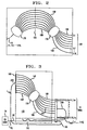
- FIG.2 is a schematic drawing of a multichannel WDM made according to silicon optical bench techniques of the prior art.
- FIG.3 is a schematic drawing of a passive optical element disclosed and claimed in the parent application EP-A-0613263 which performs broadcast and wavelength-selective signal distribution.
- FIG.4 is a schematic drawing of a passive optical element according to the invention in which the use of a bypass waveguide separates signals for broadcast distribution from signals for wavelength-selective distribution.
- FIG.5 shows a variation of the optical element of FIG.4.
- FIG. 2 Depicted in FIG. 2 is a multichannel, dense, 1 ⁇ N WDM made according to silicon optical bench methods of the prior art Components of this kind are described, for example, in C. Dragone et al., "Efficient Multichannel Integrated Optics Star Coupler on Silicon", IEEE Photon. Technol. Lett. 1 (1989) 241 - 243, and in C. Dragone et al., "Integrated Optics N ⁇ N Multiplexer on Silicon", IEEE Photon. Technol. Lett. 3 (1991) 896 - 899. Free-space N ⁇ N star couplers, made using similar technology, are described in C. Dragone, "Efficient N ⁇ N Star Couplers Using Fourier Optics", IEEE J. Lightwave Technol.
- the WDM of FIG. 2 is an interferometric device.
- two N ⁇ M couplers are interconnected by a plurality of waveguides 100 having different lengths.
- signals of various wavelengths that are input to the WDM on waveguide 110 are distributed into output waveguides 120 such that signals falling in different wavelength bands are distributed to different output waveguides.
- such a component can be used to multiplex signals in 16 or more different wavelength subchannels, with a subchannel separation of 1 - 2 nm, a cross-talk level of about -20 to -40 dB, and insertion loss of about 2.5 dB.
- the output wavelength bands are expected to exhibit a temperature drift of only about 0.014 nm/°C, permitting operation at remote, e.g., curbside, locations.
- the WDM array of FIG. 2 is substantially symmetrical about plane 130, indicated as a dashed line in the figure.
- a more compact WDM can be derived from the WDM of FIG. 2 by removing that portion of the WDM that lies to the left of plane 130 (as viewed in the figure) and replacing it by a reflector or series of reflectors that reflect light back along the remaining portions of waveguides 100.
- This arrangement is depicted as optical element 135 of FIG. 3.
- waveguides 140 which have varying lengths, are shown terminated by a reflecting surface. This arrangement can be made, e.g., by first fabricating the full WDM of FIG. 2.
- the silicon substrate of this WDM is then, e.g., sawed along plane 130, and the resulting face 160 is polished.
- this face is desirably coated with a reflective material.
- a metallic mirror usefully covers the ends of all of waveguides 140 except for the central waveguide 200.
- a multilayer dielectric mirror covers all of the waveguides, including waveguide 200. This mirror coating is designed to transmit the primary signals and reflect the secondary signals.
- ⁇ can be made less than 0.5 nm in a WDM operating at a wavelength of 1.55 ⁇ m and having path-length differences that vary in units of 150 ⁇ m, if ⁇ is less than about 0.017°.
- ⁇ can be made less than 0.5 nm in a WDM operating at a wavelength of 1.55 ⁇ m and having path-length differences that vary in units of 150 ⁇ m, if ⁇ is less than about 0.017°.
- ⁇ can be made less than 0.5 nm in a WDM operating at a wavelength of 1.55 ⁇ m and having path-length differences that vary in units of 150 ⁇ m, if ⁇ is less than about 0.017°.
- optical element of FIG. 3 At central office 70, two kinds of optical signals, occupying different wavelength bands, can be injected into feeder fiber 60. These signals are denoted “primary signals”, assigned to Ch. 1 as discussed above, and “secondary signals", assigned to Ch. 2.
- the primary and secondary signals are separated by 2-channel WDM 190, analogous to WDM 20 of FIG. 1.
- coarse WDM 190 is integrated on the same substrate as optical element 135, using silicon optical bench techniques.
- coarse WDM 190 is a separate, exemplarily optical-fiber-based, component optically coupled to element 135 by an optical fiber.
- the primary signals are delivered to waveguide 200, which will typically be the center waveguide of the waveguide array that includes waveguides 140.
- These primary signals are exemplarily delivered by optical fiber 195, which is coupled at one end to the Ch. 1 output port at the output end of WDM 190, and at the other end to the terminus of waveguide 200 at face 160.
- Fiber 195 may be aligned to waveguide 200 through an uncoated, central slot in face 160, or through a dielectric-coated mirror, as discussed above.
- element 135 functions as a broadcast coupler, and distributes these signals into all of waveguides 180, which are optically coupled to distribution fibers 90 of FIG 1. In performing this function, element 135 is analogous to broadcast coupler 10 of FIG. 1.
- a single input fiber 195 is shown in the figure, multiple such input fibers are also readily provided and coupled to multiple waveguides 200.
- the secondary signals are split off from the primary signals in WDM 190.
- the secondary signals are then directed into waveguide 210, which will typically be the center waveguide of the array which includes waveguides 180.
- These secondary signals are exemplarily delivered by optical fiber 220, which is optically coupled at one end to the Ch. 2 output port at the output end of WDM 190 and at the other end to the end of waveguide 210 distal free-space region 170.
- element 135 functions as a dense WDM.
- secondary signals in each subchannel are directed into a particular one of waveguides 180, and from each such waveguide into a corresponding distribution fiber 90.
- element 135 is analogous to dense WDM 40 in combination with coarse WDMs 30 of FIG. 1.
- a single input fiber 220 is shown in the figure, multiple such input fibers are also readily provided and coupled to multiple waveguides 210.
- element 135 can be made without any waveguide crossovers, and thus crossover losses and crosstalk can be avoided.
- waveguides 140 will number about 65 for, e.g., a 1 x 17 WDM.
- the same number of waveguides 180 will also generally be available; however, to avoid signal crosstalk, it will often be advisable to use, e.g., only one-fourth of those waveguides.
- those waveguides 180 that are active will typically number about 16, and will therefore couple to distribution fibers serving, typically, 16 ONUs.
- coarse WDM 190 is optionally a Mach-Zehnder WDM integrated on the same substrate as element 135.
- An optional, second coarse WDM is readily incorporated on the same substrate and concatenated with WDM 190 to further isolate Ch. 1 from Ch. 2.
- the Ch. 1 signals are delivered from WDM 190 to the input end of waveguide 200. This is most simply accomplished by removing the reflective material (if used) from the end of the waveguide. However, if this end is not reflective, waveguide 200 will not participate with waveguides 140 as part of the grating region of element 135 (functioning as a WDM). As a consequence, the passband corresponding to each of the subchannels will be broadened by an enhancement of sidelobe structure adjacent the corresponding transmission peak. This, in turn, can increase the crosstalk between adjacent channels. Roughly speaking, removing the central waveguide from the grating will add about 1 / M 2 of crosstalk, where M is the number of waveguides 140 in the grating region. This contribution can be reduced by including an appropriate, reflective, dielectric coating on the end of waveguide 200, or by including a Bragg reflector having a passband exemplarily about 30 nm wide.
- Table 1 lists the estimated optical losses in the network of FIG. 1 and the network of FIG. 3. The losses in the network of FIG. 3 are calculated assuming 100% reflection at the sawed and polished edge of element 135.
- element 135 must function as both a broadcast coupler (which splits optical power among multiple outputs) and a WDM, there is a design tradeoff between insertion loss (which is important for power management) and interchannel crosstalk.
- crosstalk can be reduced by increasing the spacing between adjacent (active) waveguides. However, this tends to increase the insertion loss. For example, we have estimated that a reduction of crosstalk from -10 dB to -40 dB will increase the insertion loss by 3 dB. This 3-dB penalty is included in the entry of Table 1 for broadcast loss in the 16 ⁇ 16 star coupler.
- the secondary signals are video-on-demand transmissions such as cable television transmissions.
- the secondary signals are diagnostic transmissions from an optical time-domain reflectometry unit (OTDR) housed, e.g., at the central office.
- OTDR optical time-domain reflectometry unit
- Conventional ODTR-based diagnostic techniques are not effective for diagnosing problems that originate at points downstream of a broadcast coupler such as coupler 10 of FIG. 1. This is because backscattered signals from each of the distribution fibers will overlap in time when they are received by the OTDR detector at the central office.
- the loss of optical power which is suffered by dividing the outbound OTDR signal among, e.g., 16 distribution fibers can reduce the signal level below a practical level for detection and analysis.
- a variable-wavelength OTDR transmitter is needed to produce diagnostic signals in multiple wavelength subchannels.
- One suitable light source for such a transmitter is a group of narrow-line lasers, each emitting light at a discrete wavelength.
- An alternate, and more preferable, light source includes one or more distributed Bragg reflector (DBR) lasers, each having a tuning range of about 8 - 10 nm.
- DBR distributed Bragg reflector
- Suitable DBR lasers are described, e.g., in T.L. Koch et al., "Continuously Tunable 1.5 ⁇ m Multiple-Quantum-Well AlInAs/GaInAsP Distributed-Bragg-Reflector Lasers", Elect. Lett. 24 (1988) 1431 - 1432.
- the laser power can be increased (by as much as about 7 dB, according to our estimates) by integrating such a laser with a semiconductor optical amplifier. Integration of this kind is described, for example, in U. Koren, et al., "High Power Laser-Amplifier Photonic Integrated Circuit for 1.48 ⁇ m Wavelength Operation", Appl. Phys. Lett. 59 (1991) 2351 - 2353.
- the fully bilateral WDM of FIG. 2 is used instead of the folded WDM of FIG. 3.
- a WDM includes first transmissive region 300, second transmissive region 310, and waveguides 320 which have different lengths and are optically coupled to regions 300 and 310.
- Coarse WDM 330 directs primary signals to region 310 through bypass fiber 340, without substantial optical coupling of these signals into region 300. As a consequence, these signals are broadcast into optical fibers 350 without wavelength selection.
- coarse WDM 330 directs secondary signals into region 300 through waveguides 360 or waveguide 370. As a consequence, these signals are selectively distributed into particular fibers 350 according to wavelength.
- region 300 is divided into an upper part 380 and a lower part 390 (as viewed in the figure), separated by a gap.
- Waveguide 340 passes through the gap without substantial optical coupling to region 300.
Abstract
Description
- The invention relates to fiber-optic communication networks, and more particularly to those networks that include passive components for routing and distributing optical transmissions.
- Optical fiber networks are increasingly important for the distribution of telephonic signals. Such systems generally involve a plurality of feeder fibers that emanate from a central office and terminate at respective remote terminals. Optical signals are transmitted over distribution fibers between each of these remote terminals and a plurality of optical network units (ONUs). Signals are transmitted optically or electrically between each ONU and, typically, 4 - 12 customer premises.
- Several network architectures have been proposed for transmitting signals between the remote terminals and the ONUs. One such architecture is the passive optical network (PON). In a PON, passive components are used to exchange signals between the feeder and distribution fibers. For example, a 1 × N broadcast coupler or a 1 × N wavelength-division multiplexer (WDM) is typically used to distribute an outbound signal from one feeder fiber into many (N is typically 16) distribution fibers.
- For simplicity, the descriptions of PONs included herein will often assume that signal transmission is bidirectional along each of the optical fibers of the PON. However, these discussions are meant to include unidirectional PONs as well. Bidirectional communication is readily achieved by operating an outbound, unidirectional PON in conjunction with an inbound, also unidirectional PON.
- Some proposed PON networks will carry both narrowband telephonic transmissions, and also broadband transmissions (such as cable television or high-definition television transmissions). However, distribution losses in a broadcast splitter (such as
coupler 10 of FIG. 1) which are tolerable for narrowband transmission may, nevertheless, result in inadequate signal levels for reception in (generally less sensitive) broadband receivers. Depicted in FIG. 1 is a PON configuration in which broadcast signals (which will typically be narrowband signals) are distributed by N ×N coupler 10. Additionally, signals in specified signal channels (distinguished by wavelength) are bypassed aroundcoupler 10 and delivered to specific ONUs. (These signals are typically broadband signals.) This configuration minimizes distribution losses in the broadband signals. - The PON configuration of FIG. 1 is described in EP-A-0546707.
- Briefly, the bypass arrangement is based on coarse, upstream
WDM 20, plural coarsedownstream WDMs 30, dense WDM 40, andplural bypass lines 50 which may be, e.g., optical fibers or planar waveguides. Each coarse WDM separates transmissions into, e.g., two relatively wide wavelength channels. One of these channels, to be referred to as Ch. 1, will typically correspond to the 1280 - 1340 nm and 1500 - 1560 nm wavelength regions. The other channel, to be referred to as Ch. 2, will typically correspond to the 1420 - 1450 nm region or the 1570 - 1600 nm region. Dense WDM 40 separates the Ch. 2 transmissions which it receives fromcoarse WDM 20 into plural (typically 16) subchannels. Each subchannel has a relatively narrow spectral width, typically about 2 nm. - For outbound, broadband transmission, one or more lasers at
central office 70 are selected or tuned to transmit at the broadband wavelengths assigned to selected ONUs 80. Coarse and dense WDMs at the central office are used to couple these- transmissions into (and out of)feeder fiber 60. For inbound, broadband transmission, a laser at each ONU is selected or tuned to transmit at the broadband wavelength assigned to that ONU. Three-decibel directional couplers are readily provided for insertion and extraction of signals at the ends ofbidirectional feeder fibers 60 anddistribution fibers 90. - As discussed in EP-A-0546707, cited above, silicon optical bench (SiOB) technology can be used to integrate the coarse and dense WDMs and the broadcast coupler on a single, silicon substrate. The resulting package would have the form of a silicon chip with optical fiber-array pigtails for making optical connections to the feeder and distribution fibers. This type of package offers considerable convenience in housing and handling.
- Further miniaturization of the components on such a chip is desirable in order to minimize the total volume of components that need to be housed at, e.g., a kerbside location.
- We have invented an implementation of the network of FIG. 1 which includes a silicon chip having a compact component for broadcast and wavelength-selective signal distribution. The design of this component uses space efficiently by taking advantage of the mirror symmetry of conventional multichannel WDMs made by SiOB techniques. In the inventive implementation, only that portion of the WDM lying on one side of the mirror plane is retained. Reflectors which effectively lie in the mirror plane reflect optical signals back through the retained portion. The same component also functions as
broadcast coupler 10 of FIG. 1. As a consequence, only one passive element needs to be formed on the silicon substrate. (A coarse, two-channel WDM is also required. This is optionally integrated on the silicon substrate. Alternatively, it can be made as a separate, exemplarily fiber-based, component.) - Accordingly, the invention in one aspect involves an optical communication network, which comprises: a primary transmitter for sending primary optical signals having at least one primary wavelength from a central location to plural remote locations; and a secondary transmitter for sending secondary optical signals, having plural secondary wavelengths, from the central location to the remote locations. Each of the remote locations corresponds to a particular secondary wavelength. The network further comprises a plurality of optical fibers, each having an upstream end and a downstream end; input means for optically coupling the upstream ends to the primary and secondary transmitters; and output means for optically coupling the downstream end of each of the fibers to a receiver at one of the remote locations. The input coupling means comprise an optical coupler which includes a first plurality of waveguides, to be denoted "A waveguides", a second plurality of waveguides, to be denoted "B waveguides", and a transmissive region intermediate and optically coupled to the A and B waveguide pluralities. At least two B waveguides, to be denoted "output waveguides", are optically coupled to respective optical fibers. At least one A waveguide is optically coupled to the primary transmitter, whereby primary signals are distributed into the the output waveguides.
- In contrast to networks of the prior art, at least one B waveguide is optically coupled to the secondary transmitter. Moreover, at least two A waveguides have different lengths and terminate, distal the intermediate region, at reflective regions such that the optical coupler selectively directs secondary signals of at least some wavelengths into particular output waveguides according to wavelength.
- FIG. 1 is a schematic drawing of an illustrative passive optical communication network in which signals in a primary wavelength band are broadcast, via a broadcast coupler, to multiple remote locations, and signals in at least one secondary wavelength band bypass the broadcast coupler and are transmitted only to selected remote locations.
- FIG.2 is a schematic drawing of a multichannel WDM made according to silicon optical bench techniques of the prior art.
- FIG.3 is a schematic drawing of a passive optical element disclosed and claimed in the parent application EP-A-0613263 which performs broadcast and wavelength-selective signal distribution.
- FIG.4 is a schematic drawing of a passive optical element according to the invention in which the use of a bypass waveguide separates signals for broadcast distribution from signals for wavelength-selective distribution.
- FIG.5 shows a variation of the optical element of FIG.4.
- Depicted in FIG. 2 is a multichannel, dense, 1 × N WDM made according to silicon optical bench methods of the prior art Components of this kind are described, for example, in C. Dragone et al., "Efficient Multichannel Integrated Optics Star Coupler on Silicon", IEEE Photon. Technol. Lett. 1 (1989) 241 - 243, and in C. Dragone et al., "Integrated Optics N × N Multiplexer on Silicon", IEEE Photon. Technol. Lett. 3 (1991) 896 - 899. Free-space N × N star couplers, made using similar technology, are described in C. Dragone, "Efficient N × N Star Couplers Using Fourier Optics", IEEE J. Lightwave Technol. 7 (1989) 479 - 489. Briefly, the WDM of FIG. 2 is an interferometric device. In effect, two N × M couplers are interconnected by a plurality of
waveguides 100 having different lengths. As a consequence, signals of various wavelengths that are input to the WDM onwaveguide 110 are distributed intooutput waveguides 120 such that signals falling in different wavelength bands are distributed to different output waveguides. Illustratively, such a component can be used to multiplex signals in 16 or more different wavelength subchannels, with a subchannel separation of 1 - 2 nm, a cross-talk level of about -20 to -40 dB, and insertion loss of about 2.5 dB. The output wavelength bands are expected to exhibit a temperature drift of only about 0.014 nm/°C, permitting operation at remote, e.g., curbside, locations. - The WDM array of FIG. 2 is substantially symmetrical about
plane 130, indicated as a dashed line in the figure. As a consequence, a more compact WDM can be derived from the WDM of FIG. 2 by removing that portion of the WDM that lies to the left of plane 130 (as viewed in the figure) and replacing it by a reflector or series of reflectors that reflect light back along the remaining portions ofwaveguides 100. This arrangement is depicted asoptical element 135 of FIG. 3. In FIG. 3,waveguides 140, which have varying lengths, are shown terminated by a reflecting surface. This arrangement can be made, e.g., by first fabricating the full WDM of FIG. 2. The silicon substrate of this WDM is then, e.g., sawed alongplane 130, and the resultingface 160 is polished. To prevent high optical loss, this face is desirably coated with a reflective material. For example, a metallic mirror usefully covers the ends of all ofwaveguides 140 except for thecentral waveguide 200. Alternatively, a multilayer dielectric mirror covers all of the waveguides, includingwaveguide 200. This mirror coating is designed to transmit the primary signals and reflect the secondary signals. - Since all of
waveguides 140 are parallel at this face, small translations offace 160 to the left or right (as viewed in the figure) ofideal mirror plane 130 will not have a significant effect on the operation of the WDM. Instead, the most significant source of alignment error is the angle δΘ betweenface 160 and plane 130 (i.e., the deviation from 90° of the angle betweenface 160 and the longitudinal waveguide axis). If δΘ is not zero, the path-length differences between thevarious waveguides 140 will deviate from their design values, leading to a wavelength shift δλ of the WDM subchannels. Illustratively, δλ can be made less than 0.5 nm in a WDM operating at a wavelength of 1.55 µm and having path-length differences that vary in units of 150 µm, if δΘ is less than about 0.017°. In fact, we believe that during lithographic processing of the WDM, it will be possible to align the waveguides, relative to the cleaved face, within a tolerance of 13 µm (0.5 mil) over a range of about 6 cm (i.e., over the usable length of a 10-cm silicon wafer). This is equivalent to an angular tolerance of 0.012° for wafers of this size. Thus, we believe that the required degree of alignment is readily achieved. - The operation of the optical element of FIG. 3 will now be described. At
central office 70, two kinds of optical signals, occupying different wavelength bands, can be injected intofeeder fiber 60. These signals are denoted "primary signals", assigned to Ch. 1 as discussed above, and "secondary signals", assigned to Ch. 2. The primary and secondary signals are separated by 2-channel WDM 190, analogous toWDM 20 of FIG. 1. In one embodiment,coarse WDM 190 is integrated on the same substrate asoptical element 135, using silicon optical bench techniques. In an alternate embodiment,coarse WDM 190 is a separate, exemplarily optical-fiber-based, component optically coupled toelement 135 by an optical fiber. - After passing through
WDM 190, the primary signals are delivered towaveguide 200, which will typically be the center waveguide of the waveguide array that includeswaveguides 140. These primary signals are exemplarily delivered byoptical fiber 195, which is coupled at one end to the Ch. 1 output port at the output end ofWDM 190, and at the other end to the terminus ofwaveguide 200 atface 160.Fiber 195 may be aligned to waveguide 200 through an uncoated, central slot inface 160, or through a dielectric-coated mirror, as discussed above. With respect to the primary signals inwaveguide 200,element 135 functions as a broadcast coupler, and distributes these signals into all ofwaveguides 180, which are optically coupled todistribution fibers 90 of FIG 1. In performing this function,element 135 is analogous to broadcastcoupler 10 of FIG. 1. Although asingle input fiber 195 is shown in the figure, multiple such input fibers are also readily provided and coupled tomultiple waveguides 200. - The secondary signals are split off from the primary signals in
WDM 190. The secondary signals are then directed intowaveguide 210, which will typically be the center waveguide of the array which includeswaveguides 180. These secondary signals are exemplarily delivered byoptical fiber 220, which is optically coupled at one end to the Ch. 2 output port at the output end ofWDM 190 and at the other end to the end ofwaveguide 210 distal free-space region 170. With respect to these secondary signals,element 135 functions as a dense WDM. As a result, secondary signals in each subchannel are directed into a particular one ofwaveguides 180, and from each such waveguide into acorresponding distribution fiber 90. In performing this function,element 135 is analogous to dense WDM 40 in combination withcoarse WDMs 30 of FIG. 1. Although asingle input fiber 220 is shown in the figure, multiple such input fibers are also readily provided and coupled tomultiple waveguides 210. - Significantly,
element 135 can be made without any waveguide crossovers, and thus crossover losses and crosstalk can be avoided. Typically,waveguides 140 will number about 65 for, e.g., a 1 x 17 WDM. The same number ofwaveguides 180 will also generally be available; however, to avoid signal crosstalk, it will often be advisable to use, e.g., only one-fourth of those waveguides. Thus, thosewaveguides 180 that are active will typically number about 16, and will therefore couple to distribution fibers serving, typically, 16 ONUs. As noted,coarse WDM 190 is optionally a Mach-Zehnder WDM integrated on the same substrate aselement 135. An optional, second coarse WDM is readily incorporated on the same substrate and concatenated withWDM 190 to further isolate Ch. 1 from Ch. 2. - As noted, the Ch. 1 signals are delivered from
WDM 190 to the input end ofwaveguide 200. This is most simply accomplished by removing the reflective material (if used) from the end of the waveguide. However, if this end is not reflective,waveguide 200 will not participate withwaveguides 140 as part of the grating region of element 135 (functioning as a WDM). As a consequence, the passband corresponding to each of the subchannels will be broadened by an enhancement of sidelobe structure adjacent the corresponding transmission peak. This, in turn, can increase the crosstalk between adjacent channels. Roughly speaking, removing the central waveguide from the grating will add about 1 / M2 of crosstalk, where M is the number ofwaveguides 140 in the grating region. This contribution can be reduced by including an appropriate, reflective, dielectric coating on the end ofwaveguide 200, or by including a Bragg reflector having a passband exemplarily about 30 nm wide. - Table 1 lists the estimated optical losses in the network of FIG. 1 and the network of FIG. 3. The losses in the network of FIG. 3 are calculated assuming 100% reflection at the sawed and polished edge of
element 135. - Because
element 135 must function as both a broadcast coupler (which splits optical power among multiple outputs) and a WDM, there is a design tradeoff between insertion loss (which is important for power management) and interchannel crosstalk. As noted, crosstalk can be reduced by increasing the spacing between adjacent (active) waveguides. However, this tends to increase the insertion loss. For example, we have estimated that a reduction of crosstalk from -10 dB to -40 dB will increase the insertion loss by 3 dB. This 3-dB penalty is included in the entry of Table 1 for broadcast loss in the 16 × 16 star coupler. - As noted, in one application of
element 135, the secondary signals are video-on-demand transmissions such as cable television transmissions. In another application, the secondary signals are diagnostic transmissions from an optical time-domain reflectometry unit (OTDR) housed, e.g., at the central office. Conventional ODTR-based diagnostic techniques are not effective for diagnosing problems that originate at points downstream of a broadcast coupler such ascoupler 10 of FIG. 1. This is because backscattered signals from each of the distribution fibers will overlap in time when they are received by the OTDR detector at the central office. Moreover, the loss of optical power which is suffered by dividing the outbound OTDR signal among, e.g., 16 distribution fibers can reduce the signal level below a practical level for detection and analysis. However, these problems are avoided by transmitting OTDR signals in different wavelength subchannels. These transmissions are not broadcast. Instead, an optical element such aselement 135 of FIG. 6 is used to direct each transmission into the distribution fiber assigned to the corresponding subchannel. As a result, broadcast losses are avoided in these transmissions. - A variable-wavelength OTDR transmitter is needed to produce diagnostic signals in multiple wavelength subchannels. One suitable light source for such a transmitter is a group of narrow-line lasers, each emitting light at a discrete wavelength. An alternate, and more preferable, light source includes one or more distributed Bragg reflector (DBR) lasers, each having a tuning range of about 8 - 10 nm. Suitable DBR lasers are described, e.g., in T.L. Koch et al., "Continuously Tunable 1.5 µm Multiple-Quantum-Well AlInAs/GaInAsP Distributed-Bragg-Reflector Lasers", Elect. Lett. 24 (1988) 1431 - 1432. The laser power can be increased (by as much as about 7 dB, according to our estimates) by integrating such a laser with a semiconductor optical amplifier. Integration of this kind is described, for example, in U. Koren, et al., "High Power Laser-Amplifier Photonic Integrated Circuit for 1.48 µm Wavelength Operation", Appl. Phys. Lett. 59 (1991) 2351 - 2353.
- According to an embodiment of the present invention, the fully bilateral WDM of FIG. 2 is used instead of the folded WDM of FIG. 3. Turning to FIGs. 4 and 5 such a WDM includes first
transmissive region 300, secondtransmissive region 310, andwaveguides 320 which have different lengths and are optically coupled toregions Coarse WDM 330 directs primary signals toregion 310 throughbypass fiber 340, without substantial optical coupling of these signals intoregion 300. As a consequence, these signals are broadcast intooptical fibers 350 without wavelength selection. By contrast,coarse WDM 330 directs secondary signals intoregion 300 throughwaveguides 360 orwaveguide 370. As a consequence, these signals are selectively distributed intoparticular fibers 350 according to wavelength. - In the embodiment of FIG.4,
region 300 is divided into anupper part 380 and a lower part 390 (as viewed in the figure), separated by a gap.Waveguide 340 passes through the gap without substantial optical coupling toregion 300.
Claims (3)
- An optical communication network, which comprises:CHARACTERIZED IN THATa) a primary transmitter for sending primary optical signals having at least one primary wavelength from a central location to plural remote locations;b) a secondary transmitter for sending secondary optical signals, having plural secondary wavelengths, from the central location to the remote locations, each of the remote locations corresponding to one of the secondary wavelengths;c) a plurality of optical fibers, each having an upstream end and a downstream end;d) input means for optically coupling the upstream ends to the primary and secondary transmitters; ande) output means for optically coupling the downstream end of each of the optical fibers to a receiver situated at one of the remote locations, wherein:f) the input coupling means comprise a Mach-Zehnder interferometer having: first and second transmissive regions (300, 310); a plurality of waveguides (320) of different lengths, to be denoted "A waveguides," extending between and optically coupled to the first and second transmissive regions; and a plurality of waveguides (350), to be denoted "B waveguides," each optically coupled at one end to the second transmissive region (310) and at the other end to a respective one of the optical fibers;g) the input coupling means further comprise means (340), to be referred to as "primary means," for optically coupling the primary transmitter to the second transmissive region such that primary signals are distributed into the B waveguides but are not substantially distributed into the A waveguides; andh) the input coupling means further comprise means (360, 370) for optically coupling the secondary transmitter to the first transmissive region, whereby at least some secondary signals are selectively directed into particular B waveguides according to wavelength.
- The network of claim 1, wherein the primary means comprise an optical waveguide, to be referred to as the "bypass waveguide," having an input end optically coupled to the primary transmitter and an output end optically coupled to the second transmissive region.
- The network of claim 2, wherein the first transmissive region is divided into first and second parts separated by a gap; each of said parts is optically coupled to the secondary transmitter and to a respective plurality of the A waveguides; and the bypass waveguide extends through the gap without substantial optical coupling to the first transmissive region.
Applications Claiming Priority (3)
| Application Number | Priority Date | Filing Date | Title |
|---|---|---|---|
| US21698 | 1993-02-24 | ||
| US08/021,698 US5440416A (en) | 1993-02-24 | 1993-02-24 | Optical network comprising a compact wavelength-dividing component |
| EP94301126A EP0613263B1 (en) | 1993-02-24 | 1994-02-16 | Optical network comprising a compact wavelength-dividing component |
Related Parent Applications (1)
| Application Number | Title | Priority Date | Filing Date |
|---|---|---|---|
| EP94301126A Division EP0613263B1 (en) | 1993-02-24 | 1994-02-16 | Optical network comprising a compact wavelength-dividing component |
Publications (2)
| Publication Number | Publication Date |
|---|---|
| EP0921648A2 true EP0921648A2 (en) | 1999-06-09 |
| EP0921648A3 EP0921648A3 (en) | 2000-05-10 |
Family
ID=21805638
Family Applications (2)
| Application Number | Title | Priority Date | Filing Date |
|---|---|---|---|
| EP94301126A Expired - Lifetime EP0613263B1 (en) | 1993-02-24 | 1994-02-16 | Optical network comprising a compact wavelength-dividing component |
| EP99102956A Withdrawn EP0921648A3 (en) | 1993-02-24 | 1994-02-16 | Optical network comprising compact wavelenght-dividing component |
Family Applications Before (1)
| Application Number | Title | Priority Date | Filing Date |
|---|---|---|---|
| EP94301126A Expired - Lifetime EP0613263B1 (en) | 1993-02-24 | 1994-02-16 | Optical network comprising a compact wavelength-dividing component |
Country Status (4)
| Country | Link |
|---|---|
| US (1) | US5440416A (en) |
| EP (2) | EP0613263B1 (en) |
| JP (1) | JP2953947B2 (en) |
| DE (1) | DE69427715T2 (en) |
Families Citing this family (94)
| Publication number | Priority date | Publication date | Assignee | Title |
|---|---|---|---|---|
| US5546483A (en) * | 1993-08-02 | 1996-08-13 | Nippon Telegraph And Telephone Corporation | Integrated optical waveguide circuit and optical branch line test system using the same |
| FR2725040A1 (en) * | 1994-09-23 | 1996-03-29 | Bruno Adrien | OPTOELECTRONIC DEVICE INCLUDING AN IMPROVED MULTI-LENGTH WAVELENGTH RECEIVER |
| US5617234A (en) * | 1994-09-26 | 1997-04-01 | Nippon Telegraph & Telephone Corporation | Multiwavelength simultaneous monitoring circuit employing arrayed-waveguide grating |
| CA2164356A1 (en) * | 1994-12-07 | 1996-06-08 | Tyco Submarine Systems Ltd. | Wavelength division multiplexed hybrid ring suitable for use in regional area networks |
| US5636300A (en) * | 1994-12-12 | 1997-06-03 | Corning Incorporated | MxO multiplex demultiplex component |
| GB2308252B (en) * | 1995-12-16 | 2000-02-23 | Northern Telecom Ltd | WDM channel insertion |
| US5689594A (en) * | 1995-12-29 | 1997-11-18 | Mci Communications Corp. | Multiple wavelength bidirectional lightwave amplifier |
| EP0794445B1 (en) * | 1996-03-06 | 2004-11-03 | Infineon Technologies AG | Device for wavelength stabilisation of an optical filter |
| US5926298A (en) * | 1996-08-30 | 1999-07-20 | Lucent Technologies Inc. | Optical multiplexer/demultiplexer having a broadcast port |
| US5745616A (en) * | 1996-11-27 | 1998-04-28 | Lucent Technologies Inc. | Waveguide grating router and method of making same having relatively small dimensions |
| JP2977024B2 (en) * | 1996-12-03 | 1999-11-10 | 日本電気株式会社 | Optical circuit for wavelength division multiplexing communication and optical transmission communication system including the same |
| DE19720852A1 (en) * | 1997-05-17 | 1998-11-26 | Hertz Inst Heinrich | Device for superimposing optical signals with different wavelengths |
| US5870512A (en) | 1997-05-30 | 1999-02-09 | Sdl, Inc. | Optimized interferometrically modulated array source |
| US6631018B1 (en) | 1997-08-27 | 2003-10-07 | Nortel Networks Limited | WDM optical network with passive pass-through at each node |
| US5911019A (en) * | 1997-09-04 | 1999-06-08 | Lucent Technologies Inc. | Method for upgrading a hybrid fiber coax network to an all fiber network |
| US5926587A (en) * | 1997-09-08 | 1999-07-20 | Lucent Technologies Inc. | Optical passband filters |
| FR2772144B1 (en) * | 1997-12-08 | 2000-02-25 | France Telecom | OPTICAL SIGNAL EXCHANGE DEVICE THROUGH AN OPTICAL FIBER |
| US6011885A (en) * | 1997-12-13 | 2000-01-04 | Lightchip, Inc. | Integrated bi-directional gradient refractive index wavelength division multiplexer |
| US6011884A (en) * | 1997-12-13 | 2000-01-04 | Lightchip, Inc. | Integrated bi-directional axial gradient refractive index/diffraction grating wavelength division multiplexer |
| US6404945B1 (en) | 1997-12-13 | 2002-06-11 | Lightchip, Inc. | Wavelength division multiplexing/demultiplexing devices using homogeneous refractive index lenses |
| US5999672A (en) * | 1997-12-13 | 1999-12-07 | Light Chip, Inc. | Integrated bi-directional dual axial gradient refractive index/diffraction grating wavelength division multiplexer |
| US6236780B1 (en) | 1997-12-13 | 2001-05-22 | Light Chip, Inc. | Wavelength division multiplexing/demultiplexing devices using dual diffractive optic lenses |
| US6271970B1 (en) | 1997-12-13 | 2001-08-07 | Lightchip, Inc. | Wavelength division multiplexing/demultiplexing devices using dual homogeneous refractive index lenses |
| US6263135B1 (en) | 1997-12-13 | 2001-07-17 | Lightchip, Inc. | Wavelength division multiplexing/demultiplexing devices using high index of refraction crystalline lenses |
| US6243513B1 (en) | 1997-12-13 | 2001-06-05 | Lightchip, Inc. | Wavelength division multiplexing/demultiplexing devices using diffractive optic lenses |
| US6298182B1 (en) | 1997-12-13 | 2001-10-02 | Light Chip, Inc. | Wavelength division multiplexing/demultiplexing devices using polymer lenses |
| US6289155B1 (en) | 1997-12-13 | 2001-09-11 | Lightchip, Inc. | Wavelength division multiplexing/demultiplexing devices using dual high index of refraction crystalline lenses |
| WO1999041629A1 (en) * | 1998-02-17 | 1999-08-19 | HEINRICH-HERTZ-INSTITUT FüR NACHRICHTENTECHNIK BERLIN GMBH | Device for superimposing optical signals with different wavelengths |
| DE19815404A1 (en) * | 1998-04-06 | 1999-10-14 | Siemens Ag | Arrangement for spatial separation and / or merging of optical wavelength channels |
| US6108471A (en) * | 1998-11-17 | 2000-08-22 | Bayspec, Inc. | Compact double-pass wavelength multiplexer-demultiplexer having an increased number of channels |
| US6275630B1 (en) | 1998-11-17 | 2001-08-14 | Bayspec, Inc. | Compact double-pass wavelength multiplexer-demultiplexer |
| US6445479B1 (en) | 1998-12-18 | 2002-09-03 | Lsi Logic Corporation | Electronically controlled optically-active device array for high-speed receiving and transmitting of fiber optic signals |
| US6829096B1 (en) | 1999-02-25 | 2004-12-07 | Confluent Photonics Corporation | Bi-directional wavelength division multiplexing/demultiplexing devices |
| US6343169B1 (en) | 1999-02-25 | 2002-01-29 | Lightchip, Inc. | Ultra-dense wavelength division multiplexing/demultiplexing device |
| US6480648B1 (en) | 1999-02-25 | 2002-11-12 | Lightchip, Inc. | Technique for detecting the status of WDM optical signals |
| US6434299B1 (en) | 1999-06-01 | 2002-08-13 | Lightchip, Inc. | Wavelength division multiplexing/demultiplexing devices having concave diffraction gratings |
| EP1157493B1 (en) * | 1999-12-29 | 2008-05-21 | Broadband Royalty Corporation | Dwdm catv return system with up-converters to prevent fiber crosstalk |
| DE60106736T2 (en) * | 2000-03-31 | 2005-11-24 | At & T Corp. | SOFT ARRANGEMENT WITH SHAFT GUIDE AND MULTIPLE INPUTS FOR BROADCAST AND MULTICAST SERVICES |
| US6415073B1 (en) | 2000-04-10 | 2002-07-02 | Lightchip, Inc. | Wavelength division multiplexing/demultiplexing devices employing patterned optical components |
| US6456758B1 (en) * | 2000-05-23 | 2002-09-24 | Jds Uniphase Corporation | Chip for separating light into different wavelengths |
| US6396575B1 (en) | 2000-05-31 | 2002-05-28 | Lucent Technologies Inc. | Test and measurement system for detecting and monitoring faults and losses in passive optical networks (PONs) |
| US6563977B1 (en) | 2000-06-27 | 2003-05-13 | Bayspec, Inc. | Compact wavelength multiplexer-demultiplexer providing low polarization sensitivity |
| US6553165B1 (en) | 2000-07-14 | 2003-04-22 | Applied Wdm, Inc. | Optical waveguide gratings |
| US6493487B1 (en) | 2000-07-14 | 2002-12-10 | Applied Wdm, Inc. | Optical waveguide transmission devices |
| WO2002027372A2 (en) * | 2000-07-14 | 2002-04-04 | Applied Wdm, Inc. | Optical waveguide transmission devices |
| GB2370370A (en) * | 2000-12-22 | 2002-06-26 | Kymata Ltd | Arrayed waveguide grating |
| US7145704B1 (en) | 2003-11-25 | 2006-12-05 | Cheetah Omni, Llc | Optical logic gate based optical router |
| US7006719B2 (en) * | 2002-03-08 | 2006-02-28 | Infinera Corporation | In-wafer testing of integrated optical components in photonic integrated circuits (PICs) |
| TW589474B (en) * | 2003-04-29 | 2004-06-01 | Au Optronics Corp | Display panel with the integrated driver circuit |
| CN101447835A (en) * | 2003-07-08 | 2009-06-03 | 中国科学技术大学 | Quantum network addressing method |
| WO2006034402A2 (en) * | 2004-09-21 | 2006-03-30 | Synta Pharmaceutical Corp. | Compounds for inflammation and immune-related uses |
| US7233442B1 (en) * | 2005-01-26 | 2007-06-19 | Aculight Corporation | Method and apparatus for spectral-beam combining of high-power fiber lasers |
| US7199924B1 (en) * | 2005-01-26 | 2007-04-03 | Aculight Corporation | Apparatus and method for spectral-beam combining of high-power fiber lasers |
| US7391561B2 (en) | 2005-07-29 | 2008-06-24 | Aculight Corporation | Fiber- or rod-based optical source featuring a large-core, rare-earth-doped photonic-crystal device for generation of high-power pulsed radiation and method |
| US7430352B2 (en) | 2005-07-29 | 2008-09-30 | Aculight Corporation | Multi-segment photonic-crystal-rod waveguides for amplification of high-power pulsed optical radiation and associated method |
| US8023823B2 (en) * | 2005-10-20 | 2011-09-20 | Fujitsu Limited | System and method for transmitting upstream traffic in an optical network |
| US7499651B2 (en) * | 2005-10-20 | 2009-03-03 | Fujitsu Limited | Upgradeable passive optical network |
| US7546036B2 (en) * | 2005-10-20 | 2009-06-09 | Fujitsu Limited | Hybrid passive optical network using shared wavelengths |
| US7653309B2 (en) * | 2005-10-20 | 2010-01-26 | Fujitsu Limited | System and method for distributing traffic in an optical network |
| US7684705B2 (en) * | 2005-10-20 | 2010-03-23 | Fujitsu Limited | Distribution node for a wavelength-sharing network |
| US7684706B2 (en) * | 2005-10-20 | 2010-03-23 | Fujitsu Limited | System and method for traffic distribution in an optical network |
| US7522838B2 (en) * | 2005-10-20 | 2009-04-21 | Fujitsu Limited | Distribution components for a wavelength-sharing network |
| US7639946B2 (en) * | 2006-01-06 | 2009-12-29 | Fujitsu Limited | Distribution node for an optical network |
| US7603036B2 (en) * | 2006-01-06 | 2009-10-13 | Fujitsu Limited | System and method for managing network components in a hybrid passive optical network |
| CN101009530B (en) * | 2006-01-23 | 2012-02-15 | 华为技术有限公司 | Passive optical network, multiplexing/de-multiplexing device and method supporting the multicast service |
| US8180223B2 (en) * | 2006-02-03 | 2012-05-15 | Fujitsu Limited | System and method for extending reach in a passive optical network |
| US7537395B2 (en) * | 2006-03-03 | 2009-05-26 | Lockheed Martin Corporation | Diode-laser-pump module with integrated signal ports for pumping amplifying fibers and method |
| US7768700B1 (en) | 2006-11-30 | 2010-08-03 | Lockheed Martin Corporation | Method and apparatus for optical gain fiber having segments of differing core sizes |
| US7715719B2 (en) * | 2006-06-02 | 2010-05-11 | Fujitsu Limited | System and method for transmitting traffic in a plurality of passive optical networks |
| US20070280690A1 (en) * | 2006-06-02 | 2007-12-06 | Fujitsu Limited | System and Method for Managing Power in an Optical Network |
| JP4899822B2 (en) * | 2006-11-27 | 2012-03-21 | 住友電気工業株式会社 | Optical multiplexer / demultiplexer |
| US8565599B2 (en) | 2006-12-11 | 2013-10-22 | Fujitsu Limited | System and method for transmitting optical markers in a passive optical network system |
| US20080138063A1 (en) * | 2006-12-11 | 2008-06-12 | Youichi Akasaka | System and Method for Protecting an Optical Network |
| US7970281B2 (en) * | 2007-01-26 | 2011-06-28 | Fujitsu Limited | System and method for managing different transmission architectures in a passive optical network |
| US7920792B2 (en) * | 2007-05-02 | 2011-04-05 | Fujitsu Limited | System and method for managing communication in a hybrid passive optical network |
| US8179594B1 (en) | 2007-06-29 | 2012-05-15 | Lockheed Martin Corporation | Method and apparatus for spectral-beam combining of fanned-in laser beams with chromatic-dispersion compensation using a plurality of diffractive gratings |
| US8175427B2 (en) * | 2007-09-18 | 2012-05-08 | Rockwell Automation Technologies, Inc. | Apparatus and methods for use of a tunable optical source in safety curtain applications |
| US7639908B2 (en) * | 2008-01-23 | 2009-12-29 | Enablence USA Components, Inc. | Broadcasting arrayed waveguide |
| US8948598B2 (en) * | 2008-02-13 | 2015-02-03 | Fujitsu Limited | System and method for increasing upstream capacity in an optical network |
| GB0823688D0 (en) * | 2008-12-31 | 2009-02-04 | Tyco Electronics Raychem Nv | Unidirectional absolute optical attenuation measurement with OTDR |
| US8526110B1 (en) | 2009-02-17 | 2013-09-03 | Lockheed Martin Corporation | Spectral-beam combining for high-power fiber-ring-laser systems |
| US8503840B2 (en) | 2010-08-23 | 2013-08-06 | Lockheed Martin Corporation | Optical-fiber array method and apparatus |
| US8441718B2 (en) * | 2009-11-23 | 2013-05-14 | Lockheed Martin Corporation | Spectrally beam combined laser system and method at eye-safer wavelengths |
| WO2011130131A1 (en) | 2010-04-12 | 2011-10-20 | Lockheed Martin Corporation | Beam diagnostics and feedback system and method for spectrally beam-combined lasers |
| US8705972B2 (en) * | 2010-05-11 | 2014-04-22 | Hewlett-Packard Development Company, L.P. | Energy-efficient and fault-tolerant resonator-based modulation and wavelength division multiplexing systems |
| EP2726837B1 (en) * | 2011-07-01 | 2018-09-05 | Telefonaktiebolaget LM Ericsson (publ) | Device, remote node and methods for pon supervision |
| US8923672B2 (en) * | 2011-11-10 | 2014-12-30 | Alcatel Lucent | Wavelength router for a passive optical network |
| US20130183035A1 (en) * | 2011-12-01 | 2013-07-18 | Joseph L. Smith | Enhanced PON And Splitter Module And Associated Method |
| US8693866B1 (en) * | 2012-01-20 | 2014-04-08 | Google Inc. | Fiber diagnosis system for WDM optical access networks |
| TWI445333B (en) * | 2012-02-29 | 2014-07-11 | Univ Nat Taiwan Science Tech | Time/wavelength-division multiplexed pon (twpon) |
| US20130315579A1 (en) * | 2012-05-25 | 2013-11-28 | Verizon Patent And Licensing Inc. | Method and system for providing a shared demarcation point to monitor network performance |
| US9835778B1 (en) | 2013-09-13 | 2017-12-05 | Lockheed Martin Corporation | Apparatus and method for a diamond substrate for a multi-layered dielectric diffraction grating |
| US9366872B2 (en) | 2014-02-18 | 2016-06-14 | Lockheed Martin Corporation | Apparatus and method for fiber-laser output-beam shaping for spectral beam combination |
| WO2019089987A1 (en) * | 2017-11-01 | 2019-05-09 | O-Net Communications (Usa) Inc. | Optical packaging and designs for optical transceivers |
Citations (2)
| Publication number | Priority date | Publication date | Assignee | Title |
|---|---|---|---|---|
| US4786133A (en) * | 1986-12-31 | 1988-11-22 | Commissariat A L'energie Atomique | Multiplexer-demultiplexer using an elliptical concave grating and produced in integrated optics |
| US5136671A (en) * | 1991-08-21 | 1992-08-04 | At&T Bell Laboratories | Optical switch, multiplexer, and demultiplexer |
Family Cites Families (6)
| Publication number | Priority date | Publication date | Assignee | Title |
|---|---|---|---|---|
| CA1271065A (en) * | 1985-07-24 | 1990-07-03 | Michael Charles Brierley | Dielectric optical waveguide device |
| US4715027A (en) * | 1986-05-29 | 1987-12-22 | Polaroid Corporation | Integrated optic multi/demultiplexer |
| US5026131A (en) * | 1988-02-22 | 1991-06-25 | Physical Optics Corporation | High channel density, broad bandwidth wavelength division multiplexer with highly non-uniform Bragg-Littrow holographic grating |
| US4902086A (en) * | 1988-03-03 | 1990-02-20 | At&T Bell Laboratories | Device including a substrate-supported optical waveguide, and method of manufacture |
| US4923271A (en) * | 1989-03-28 | 1990-05-08 | American Telephone And Telegraph Company | Optical multiplexer/demultiplexer using focusing Bragg reflectors |
| US5243672A (en) * | 1992-08-04 | 1993-09-07 | At&T Bell Laboratories | Planar waveguide having optimized bend |
-
1993
- 1993-02-24 US US08/021,698 patent/US5440416A/en not_active Expired - Lifetime
-
1994
- 1994-02-16 EP EP94301126A patent/EP0613263B1/en not_active Expired - Lifetime
- 1994-02-16 EP EP99102956A patent/EP0921648A3/en not_active Withdrawn
- 1994-02-16 DE DE69427715T patent/DE69427715T2/en not_active Expired - Lifetime
- 1994-02-21 JP JP6044682A patent/JP2953947B2/en not_active Expired - Lifetime
Patent Citations (2)
| Publication number | Priority date | Publication date | Assignee | Title |
|---|---|---|---|---|
| US4786133A (en) * | 1986-12-31 | 1988-11-22 | Commissariat A L'energie Atomique | Multiplexer-demultiplexer using an elliptical concave grating and produced in integrated optics |
| US5136671A (en) * | 1991-08-21 | 1992-08-04 | At&T Bell Laboratories | Optical switch, multiplexer, and demultiplexer |
Non-Patent Citations (1)
| Title |
|---|
| HILL A M: "AN EXPERIMENTAL BROADBAND AND TELEPHONY PASSIVE OPTICAL NETWORK" PROCEEDINGS OF THE GLOBAL TELECOMMUNICATIONS CONFERENCE AND EXHIBITION(GLOBECOM),US,NEW YORK, IEEE, vol. -, 1991, pages 1856-1860, XP000218890 ISBN: 0-87942-632-2 * |
Also Published As
| Publication number | Publication date |
|---|---|
| US5440416A (en) | 1995-08-08 |
| EP0613263B1 (en) | 2001-07-18 |
| EP0613263A1 (en) | 1994-08-31 |
| JPH077476A (en) | 1995-01-10 |
| JP2953947B2 (en) | 1999-09-27 |
| DE69427715T2 (en) | 2002-06-13 |
| EP0921648A3 (en) | 2000-05-10 |
| DE69427715D1 (en) | 2001-08-23 |
Similar Documents
| Publication | Publication Date | Title |
|---|---|---|
| EP0613263B1 (en) | Optical network comprising a compact wavelength-dividing component | |
| US6404948B2 (en) | Dense WDM optical multiplexer and demultiplexer | |
| US11929826B2 (en) | Optical modules having an improved optical signal to noise ratio | |
| US6185023B1 (en) | Optical add-drop multiplexers compatible with very dense WDM optical communication systems | |
| US8285144B2 (en) | Optical device for rearranging wavelength channels | |
| US6959129B2 (en) | Bidirectional multiplexer and demultiplexer based on a single echelle waveguide grating | |
| US11624879B2 (en) | Multi-channel optical coupler | |
| US6567196B1 (en) | Dense WDM optical multiplexer and demultiplexer | |
| EP3271977B1 (en) | Tunable laser including parallel lasing cavities with a common output | |
| US7386235B2 (en) | Protocol and line-rate transparent WDM passive optical network | |
| US7171081B1 (en) | Plug-in coupler to convert the transceiver (transmitter/receiver, tx/rx) transmission into a bi-directional fiber | |
| CN104115047A (en) | Optical slab | |
| US6552834B2 (en) | Methods and apparatus for preventing deadbands in an optical communication system | |
| US20230353251A1 (en) | Photonic Integrated Circuit for High-Wavelength-Channel-Count Wavelength-Division-Multiplexed Systems | |
| JP4116244B2 (en) | Transceiver for wavelength division multiplexing | |
| US20100086307A1 (en) | Planar lightwave circuit | |
| KR100901508B1 (en) | Light source distributor for use in wavelength division multiplexed-passive optical network | |
| JP4140664B2 (en) | Optical module for access network for broadband communication system and related manufacturing method | |
| US20230291493A1 (en) | Wavelength-Multiplexed Optical Source with Reduced Temperature Sensitivity | |
| US20060291858A1 (en) | Bi-directional compound-WDM fiberoptic system architecture with redundancy protection for transmission of data, voice and video signals | |
| JP2004072690A (en) | Optical communication system | |
| WO2004036794A1 (en) | Optical modulation devices | |
| KR20190002233A (en) | Optical module for convergence of different service |
Legal Events
| Date | Code | Title | Description |
|---|---|---|---|
| PUAI | Public reference made under article 153(3) epc to a published international application that has entered the european phase |
Free format text: ORIGINAL CODE: 0009012 |
|
| 17P | Request for examination filed |
Effective date: 19990225 |
|
| AC | Divisional application: reference to earlier application |
Ref document number: 613263 Country of ref document: EP |
|
| AK | Designated contracting states |
Kind code of ref document: A2 Designated state(s): DE FR GB IT |
|
| RIN1 | Information on inventor provided before grant (corrected) |
Inventor name: YAFFE, HENRY HOWARD Inventor name: KAZARINOV, RUDOLF FEODOR Inventor name: HENRY, CHARLES HOWARD Inventor name: COHEN, LEONARD GEORGE |
|
| PUAL | Search report despatched |
Free format text: ORIGINAL CODE: 0009013 |
|
| AK | Designated contracting states |
Kind code of ref document: A3 Designated state(s): DE FR GB IT |
|
| RIC1 | Information provided on ipc code assigned before grant |
Free format text: 7H 04B 10/213 A, 7G 02B 6/34 B, 7H 04B 10/207 B |
|
| 17Q | First examination report despatched |
Effective date: 20090731 |
|
| STAA | Information on the status of an ep patent application or granted ep patent |
Free format text: STATUS: THE APPLICATION HAS BEEN WITHDRAWN |
|
| 18W | Application withdrawn |
Effective date: 20120229 |