EP0920995A2 - Method of producing ink jet head valve, method of producing ink jet head and ink jet head produced by the method - Google Patents
Method of producing ink jet head valve, method of producing ink jet head and ink jet head produced by the method Download PDFInfo
- Publication number
- EP0920995A2 EP0920995A2 EP98122941A EP98122941A EP0920995A2 EP 0920995 A2 EP0920995 A2 EP 0920995A2 EP 98122941 A EP98122941 A EP 98122941A EP 98122941 A EP98122941 A EP 98122941A EP 0920995 A2 EP0920995 A2 EP 0920995A2
- Authority
- EP
- European Patent Office
- Prior art keywords
- jet head
- ink jet
- valve
- ink
- producing
- Prior art date
- Legal status (The legal status is an assumption and is not a legal conclusion. Google has not performed a legal analysis and makes no representation as to the accuracy of the status listed.)
- Granted
Links
- 238000000034 method Methods 0.000 title claims abstract description 53
- 230000008569 process Effects 0.000 claims abstract description 30
- 238000007599 discharging Methods 0.000 claims abstract description 25
- 229910052751 metal Inorganic materials 0.000 claims abstract description 19
- 239000002184 metal Substances 0.000 claims abstract description 19
- 239000000758 substrate Substances 0.000 claims description 23
- NJPPVKZQTLUDBO-UHFFFAOYSA-N novaluron Chemical compound C1=C(Cl)C(OC(F)(F)C(OC(F)(F)F)F)=CC=C1NC(=O)NC(=O)C1=C(F)C=CC=C1F NJPPVKZQTLUDBO-UHFFFAOYSA-N 0.000 claims description 19
- 230000000873 masking effect Effects 0.000 claims description 12
- 229910052721 tungsten Inorganic materials 0.000 claims description 9
- 238000005530 etching Methods 0.000 claims description 6
- 229910052804 chromium Inorganic materials 0.000 claims description 4
- 229910052742 iron Inorganic materials 0.000 claims description 4
- 229910052748 manganese Inorganic materials 0.000 claims description 4
- 229910052750 molybdenum Inorganic materials 0.000 claims description 4
- 229910052759 nickel Inorganic materials 0.000 claims description 4
- 230000006835 compression Effects 0.000 claims description 3
- 238000007906 compression Methods 0.000 claims description 3
- 229910052697 platinum Inorganic materials 0.000 claims description 3
- 229910052715 tantalum Inorganic materials 0.000 claims description 3
- 239000007788 liquid Substances 0.000 description 61
- 239000010408 film Substances 0.000 description 26
- 238000010438 heat treatment Methods 0.000 description 21
- 239000000463 material Substances 0.000 description 20
- WFKWXMTUELFFGS-UHFFFAOYSA-N tungsten Chemical compound [W] WFKWXMTUELFFGS-UHFFFAOYSA-N 0.000 description 6
- 239000010937 tungsten Substances 0.000 description 6
- XUIMIQQOPSSXEZ-UHFFFAOYSA-N Silicon Chemical compound [Si] XUIMIQQOPSSXEZ-UHFFFAOYSA-N 0.000 description 5
- 239000010703 silicon Substances 0.000 description 5
- 229910052710 silicon Inorganic materials 0.000 description 5
- KRHYYFGTRYWZRS-UHFFFAOYSA-N Fluorane Chemical compound F KRHYYFGTRYWZRS-UHFFFAOYSA-N 0.000 description 4
- 238000004519 manufacturing process Methods 0.000 description 4
- 238000000206 photolithography Methods 0.000 description 4
- 238000011144 upstream manufacturing Methods 0.000 description 4
- 229910052581 Si3N4 Inorganic materials 0.000 description 3
- VYPSYNLAJGMNEJ-UHFFFAOYSA-N Silicium dioxide Chemical compound O=[Si]=O VYPSYNLAJGMNEJ-UHFFFAOYSA-N 0.000 description 3
- 230000008859 change Effects 0.000 description 3
- 238000005516 engineering process Methods 0.000 description 3
- 229910000040 hydrogen fluoride Inorganic materials 0.000 description 3
- 238000007747 plating Methods 0.000 description 3
- HQVNEWCFYHHQES-UHFFFAOYSA-N silicon nitride Chemical compound N12[Si]34N5[Si]62N3[Si]51N64 HQVNEWCFYHHQES-UHFFFAOYSA-N 0.000 description 3
- 229910052814 silicon oxide Inorganic materials 0.000 description 3
- BLRPTPMANUNPDV-UHFFFAOYSA-N Silane Chemical compound [SiH4] BLRPTPMANUNPDV-UHFFFAOYSA-N 0.000 description 2
- 230000009471 action Effects 0.000 description 2
- 230000008901 benefit Effects 0.000 description 2
- 238000009835 boiling Methods 0.000 description 2
- 239000005380 borophosphosilicate glass Substances 0.000 description 2
- 230000005587 bubbling Effects 0.000 description 2
- 238000006073 displacement reaction Methods 0.000 description 2
- 230000000694 effects Effects 0.000 description 2
- 238000005323 electroforming Methods 0.000 description 2
- -1 for example Substances 0.000 description 2
- 239000007789 gas Substances 0.000 description 2
- 230000006872 improvement Effects 0.000 description 2
- 229910010272 inorganic material Inorganic materials 0.000 description 2
- 239000011147 inorganic material Substances 0.000 description 2
- 239000011368 organic material Substances 0.000 description 2
- 238000000059 patterning Methods 0.000 description 2
- 238000005268 plasma chemical vapour deposition Methods 0.000 description 2
- LIVNPJMFVYWSIS-UHFFFAOYSA-N silicon monoxide Chemical compound [Si-]#[O+] LIVNPJMFVYWSIS-UHFFFAOYSA-N 0.000 description 2
- 238000004544 sputter deposition Methods 0.000 description 2
- 239000010409 thin film Substances 0.000 description 2
- MHAJPDPJQMAIIY-UHFFFAOYSA-N Hydrogen peroxide Chemical compound OO MHAJPDPJQMAIIY-UHFFFAOYSA-N 0.000 description 1
- 238000009825 accumulation Methods 0.000 description 1
- 230000005540 biological transmission Effects 0.000 description 1
- 230000015572 biosynthetic process Effects 0.000 description 1
- 229910052802 copper Inorganic materials 0.000 description 1
- 238000000151 deposition Methods 0.000 description 1
- 239000013013 elastic material Substances 0.000 description 1
- 239000011810 insulating material Substances 0.000 description 1
- 238000009413 insulation Methods 0.000 description 1
- 150000002739 metals Chemical class 0.000 description 1
- 238000005457 optimization Methods 0.000 description 1
- 230000001681 protective effect Effects 0.000 description 1
- 239000011347 resin Substances 0.000 description 1
- 229920005989 resin Polymers 0.000 description 1
Images


Classifications
-
- B—PERFORMING OPERATIONS; TRANSPORTING
- B41—PRINTING; LINING MACHINES; TYPEWRITERS; STAMPS
- B41J—TYPEWRITERS; SELECTIVE PRINTING MECHANISMS, i.e. MECHANISMS PRINTING OTHERWISE THAN FROM A FORME; CORRECTION OF TYPOGRAPHICAL ERRORS
- B41J2/00—Typewriters or selective printing mechanisms characterised by the printing or marking process for which they are designed
- B41J2/005—Typewriters or selective printing mechanisms characterised by the printing or marking process for which they are designed characterised by bringing liquid or particles selectively into contact with a printing material
- B41J2/01—Ink jet
- B41J2/135—Nozzles
- B41J2/16—Production of nozzles
- B41J2/1621—Manufacturing processes
- B41J2/164—Manufacturing processes thin film formation
- B41J2/1642—Manufacturing processes thin film formation thin film formation by CVD [chemical vapor deposition]
-
- B—PERFORMING OPERATIONS; TRANSPORTING
- B41—PRINTING; LINING MACHINES; TYPEWRITERS; STAMPS
- B41J—TYPEWRITERS; SELECTIVE PRINTING MECHANISMS, i.e. MECHANISMS PRINTING OTHERWISE THAN FROM A FORME; CORRECTION OF TYPOGRAPHICAL ERRORS
- B41J2/00—Typewriters or selective printing mechanisms characterised by the printing or marking process for which they are designed
- B41J2/005—Typewriters or selective printing mechanisms characterised by the printing or marking process for which they are designed characterised by bringing liquid or particles selectively into contact with a printing material
- B41J2/01—Ink jet
- B41J2/135—Nozzles
- B41J2/14—Structure thereof only for on-demand ink jet heads
- B41J2/14016—Structure of bubble jet print heads
- B41J2/14032—Structure of the pressure chamber
- B41J2/14048—Movable member in the chamber
-
- B—PERFORMING OPERATIONS; TRANSPORTING
- B41—PRINTING; LINING MACHINES; TYPEWRITERS; STAMPS
- B41J—TYPEWRITERS; SELECTIVE PRINTING MECHANISMS, i.e. MECHANISMS PRINTING OTHERWISE THAN FROM A FORME; CORRECTION OF TYPOGRAPHICAL ERRORS
- B41J2/00—Typewriters or selective printing mechanisms characterised by the printing or marking process for which they are designed
- B41J2/005—Typewriters or selective printing mechanisms characterised by the printing or marking process for which they are designed characterised by bringing liquid or particles selectively into contact with a printing material
- B41J2/01—Ink jet
- B41J2/135—Nozzles
- B41J2/16—Production of nozzles
- B41J2/1601—Production of bubble jet print heads
- B41J2/1604—Production of bubble jet print heads of the edge shooter type
-
- B—PERFORMING OPERATIONS; TRANSPORTING
- B41—PRINTING; LINING MACHINES; TYPEWRITERS; STAMPS
- B41J—TYPEWRITERS; SELECTIVE PRINTING MECHANISMS, i.e. MECHANISMS PRINTING OTHERWISE THAN FROM A FORME; CORRECTION OF TYPOGRAPHICAL ERRORS
- B41J2/00—Typewriters or selective printing mechanisms characterised by the printing or marking process for which they are designed
- B41J2/005—Typewriters or selective printing mechanisms characterised by the printing or marking process for which they are designed characterised by bringing liquid or particles selectively into contact with a printing material
- B41J2/01—Ink jet
- B41J2/135—Nozzles
- B41J2/16—Production of nozzles
- B41J2/1621—Manufacturing processes
- B41J2/1626—Manufacturing processes etching
-
- B—PERFORMING OPERATIONS; TRANSPORTING
- B41—PRINTING; LINING MACHINES; TYPEWRITERS; STAMPS
- B41J—TYPEWRITERS; SELECTIVE PRINTING MECHANISMS, i.e. MECHANISMS PRINTING OTHERWISE THAN FROM A FORME; CORRECTION OF TYPOGRAPHICAL ERRORS
- B41J2/00—Typewriters or selective printing mechanisms characterised by the printing or marking process for which they are designed
- B41J2/005—Typewriters or selective printing mechanisms characterised by the printing or marking process for which they are designed characterised by bringing liquid or particles selectively into contact with a printing material
- B41J2/01—Ink jet
- B41J2/135—Nozzles
- B41J2/16—Production of nozzles
- B41J2/1621—Manufacturing processes
- B41J2/1631—Manufacturing processes photolithography
-
- B—PERFORMING OPERATIONS; TRANSPORTING
- B41—PRINTING; LINING MACHINES; TYPEWRITERS; STAMPS
- B41J—TYPEWRITERS; SELECTIVE PRINTING MECHANISMS, i.e. MECHANISMS PRINTING OTHERWISE THAN FROM A FORME; CORRECTION OF TYPOGRAPHICAL ERRORS
- B41J2/00—Typewriters or selective printing mechanisms characterised by the printing or marking process for which they are designed
- B41J2/005—Typewriters or selective printing mechanisms characterised by the printing or marking process for which they are designed characterised by bringing liquid or particles selectively into contact with a printing material
- B41J2/01—Ink jet
- B41J2/135—Nozzles
- B41J2/16—Production of nozzles
- B41J2/1621—Manufacturing processes
- B41J2/164—Manufacturing processes thin film formation
- B41J2/1645—Manufacturing processes thin film formation thin film formation by spincoating
-
- B—PERFORMING OPERATIONS; TRANSPORTING
- B41—PRINTING; LINING MACHINES; TYPEWRITERS; STAMPS
- B41J—TYPEWRITERS; SELECTIVE PRINTING MECHANISMS, i.e. MECHANISMS PRINTING OTHERWISE THAN FROM A FORME; CORRECTION OF TYPOGRAPHICAL ERRORS
- B41J2/00—Typewriters or selective printing mechanisms characterised by the printing or marking process for which they are designed
- B41J2/005—Typewriters or selective printing mechanisms characterised by the printing or marking process for which they are designed characterised by bringing liquid or particles selectively into contact with a printing material
- B41J2/01—Ink jet
- B41J2/135—Nozzles
- B41J2/16—Production of nozzles
- B41J2/1621—Manufacturing processes
- B41J2/164—Manufacturing processes thin film formation
- B41J2/1646—Manufacturing processes thin film formation thin film formation by sputtering
-
- Y—GENERAL TAGGING OF NEW TECHNOLOGICAL DEVELOPMENTS; GENERAL TAGGING OF CROSS-SECTIONAL TECHNOLOGIES SPANNING OVER SEVERAL SECTIONS OF THE IPC; TECHNICAL SUBJECTS COVERED BY FORMER USPC CROSS-REFERENCE ART COLLECTIONS [XRACs] AND DIGESTS
- Y10—TECHNICAL SUBJECTS COVERED BY FORMER USPC
- Y10T—TECHNICAL SUBJECTS COVERED BY FORMER US CLASSIFICATION
- Y10T29/00—Metal working
- Y10T29/49—Method of mechanical manufacture
- Y10T29/49401—Fluid pattern dispersing device making, e.g., ink jet
Definitions
- the present invention relates to a method of producing an ink jet head valve, a method of producing an ink jet head and an ink jet head produced by the method.
- An ink jet recording process so called a bubble jet recording process, in which a state change including a rapid volume change of ink (i.e., generation of bubbles) is caused to generate by imparting energy such as heat or the like to the ink, the ink is discharged from a discharge port by an active force due to this state change and the discharged ink is adhered to a medium to be recorded to perform an image formation, has been well known.
- a state change including a rapid volume change of ink i.e., generation of bubbles
- the ink is discharged from a discharge port by an active force due to this state change and the discharged ink is adhered to a medium to be recorded to perform an image formation
- a high quality level image can be recorded at high speed and low noise and a discharge port for discharging ink can be provided at high density in a head in this recording process. Therefore, the recording process has a number of the advantages that a high revolution recording image and such color image could easily be obtained in a compact device.
- this bubble jet recording process has recently been used in various office equipment such as a printer, copy machine, facsimile and the like. Further, the recording process is used even in an industrial system such as a printing equipment etc.
- an answer to demand of improvement of energy efficiency includes optimization of a heating element in which thickness of a protective film is controlled.
- This technology has an advantage in that the transmission efficiency of generated heat to liquid is enhanced.
- a driving condition for imparting a liquid discharging method in which an improved ink discharge based on a stable bubble generation can be performed. Furthermore, to obtain a liquid discharge head having a high refilling speed of a discharged liquid to a liquid flow path from the viewpoint of the high speed recording, there is also provided a liquid discharge head having improved shapes of the liquid flow path.
- a flow path structure and a head producing method disclosed in Japanese Patent Laid-open Application No. 63-199972, relating to the shapes of the flow path, are inventions directed to a back wave (pressure in a direction opposite to that toward a discharge port, that is pressure toward a liquid chamber) which is generated with the generation bubbles.
- This back wave is known as a loss energy since it is not an energy toward the discharge direction.
- a head disclosed in the Japanese Patent Laid-open Application No. 63-199972 has an ink jet head valve which is spaced from a bubbling area of bubbles formed by the heating element and is positioned at the opposite side to the discharge port with respect to the heating element.
- This valve has an initial position in a manner that it is adhered to the ceiling of the flow path by a head producing method using a plate material, and is hung down in the flow path with the generation of bubbles.
- This application discloses an invention in which an energy loss is controlled by controlling a part of the above-mentioned back wave with a valve.
- the Japanese Patent Laid-open Application No. 9-201966 discloses a constitution in which a movable member is provided facing a bubble generation area which generates bubbles, and the growth of bubbles is controlled by using displacement of the movable member, generated by pressure at the time of bubble generation.
- Fig. 4 shows a partially broken perspective view of one embodiment of a liquid discharging head provided with such ink jet head valve.
- a heating element 2 which allows a heat energy to act on liquid is provided on an element substrate 1 as a discharge energy generating element for discharging liquid.
- Liquid flow paths 7 are provided on this element substrate 1 correspondingly to the heating element 2.
- the liquid flow paths 7 are communicated with a discharge port 5, and are also communicated with a common liquid chamber 13 for supplying liquid to the plurality of liquid flow paths 7, thereby receiving an amount of liquid corresponding to the liquid discharged from a discharge port, from this common liquid chamber 13.
- an ink jet head valve in which a 1 ⁇ m thick plate-shaped movable member 6 having a flat surface portion, which is composed of an elastic material, such as a thin film resin, metal or the like, is provided like a cantilever beam.
- Fig. 4 when the heating element 2 is heated, heat is acted on liquid in a bubble generation region between the movable member 6 and heating element, thereby generating bubbles based on the film boiling phenomena.
- the pressure and bubbles based on the generation of bubbles act on the movable member 6 and cause the member 6 to displace so that the member is largely opened on a liquid discharge side using a fulcrum 6a as the center of rotation, whereby the pressure generated by generation of bubbles and the bubbles themselves can be led to the down stream side where the discharge port 5 is provided.
- valve material produced by an electroforming process or the like was used to laminate the material on a substrate.
- valve material When the valve material is laminated on the substrate, it is necessary to provide a space of about 1 to 20 ⁇ m between the movable member and heating element so as to sufficiently obtain effects of the movable member. Further, to laminate the valve material produced by the electroforming process or the like so that a space can be formed in the movable portions, it is necessary to form a pedestal portion on the substrate so that a valve is previously fixed onto the substrate.
- the pedestal portion having for example 5 ⁇ m, which is merely the height of the space, and to prevent the pedestal portion from being corroded with ink, it is necessary to form the portion by an Au plating process or the like.
- Au plating sputtering of Au and patterning thereof by the photolithography technology are needed.
- the objects of the present invention are to solve the above-mentioned problems and provide a method of producing an improved ink jet head valve, a method of producing an ink jet head, and an ink jet head produced by the method.
- an ink jet head valve for an ink jet head having a discharge port for discharging ink, an ink flow path communicated with said discharge port and an electrothermal converting member used as an energy generating means for discharging ink into said ink flow path, comprising the step of producing said ink jet head valve by a metal CVD process.
- a method of producing an ink jet head having a discharge port for discharging ink, an ink flow path communicated with said discharge port and an electrothermal converting member used as an energy generating means for discharging ink into said ink flow path comprising the step of:
- an ink jet head produced by the above-mentioned method.
- the ink jet head valve and ink jet head are produced by using Ta, W, Pt, Mo, Cr, Mn, Fe, Co, Ni, or Cu.
- the conducting layer is formed by compression stress and said movable member is formed by tensile stress.
- Figs. 1A to 1E and Figs. 2F to 2J are cross-sectional views showing the first half and last half production steps of an ink jet head valve according to the present invention, respectively.
- a pedestal of a valve on a substrate, an about 5 ⁇ m thick PSG film is formed on a Ta film used as an anti-cavitation film at a temperature of 350 °C by a plasma CVD process (Fig. 1A). Then, to perform patterning of the PSG film by the photolithography process, resist is spin-coated on the PSG film to form a resist film thereon. After that a predetermined portion of the resist layer is exposed and developed. In this case, as a film material for forming the pedestal of a valve, PSG was used.
- the material is not limited to PSG, other materials such as an inorganic material, for example, BPSG, or SiO or the like, or an organic material may be used, if such material is not changed in quality in a metal CVD process which will be described later.
- the PSG film is etched by a buffered hydrogen fluoride to form a desired PSG film pattern (Fig. 1B).
- the tungsten film is selectively formed only on an exposed Ta portion, thereby forming a pedestal of a valve (Fig. 1C).
- W is selected as the material of the pedestal of a valve
- the material is not limited to W, Ta, Pt, Mo, Cr, Mn, Fe, Co, Ni, Cu, or the like may be used, if they have functions as the materials of the valve pedestal and the valve itself. Alternatively, the materials of the pedestal and valve may be varied according to functions.
- an 1000 angstrom thick Ni wiring layer by a sputtering process (Fig. 1D).
- the Ni wiring layer is used for forming a valve material using a metal CVD process.
- the wiring layer was formed with Pd.
- other metals may be used.
- an about 5 ⁇ m thick PSG film is formed by a plasma CVD process (Fig. 1E.
- the insulating film a PSG film was used.
- the insulating material is not limited to PSG, other materials such as an inorganic material, for example, BPSG, or SiO or the like, or an organic material may be used, if such material is not changed in quality in a metal CVD process which will be described later.
- the PSG film is etched by a buffered hydrogen fluoride (HF) to form a desired PSG film pattern (Fig. 2F).
- HF buffered hydrogen fluoride
- W selective tungsten
- the tungsten film is selectively formed only on an exposed Pd portion, thereby forming a valve (Fig. 2G).
- a previously curved valve having a cross-sectional view of Fig. 5 not Fig. 2J can be formed as the final configuration.
- an underlying wiring layer is formed by a compression stress of 1 ⁇ 10 9 dyn/cm 2 and the metal layer on the metal CVD side is formed by a tensile stress of 1 ⁇ 10 9 dyn/cm 2
- the valve is deformed so that it is warped on the metal CVD side as shown in Fig. 5.
- formed valve does not require power to deform the valve during bubbling and can be moved only at the time of refilling. Therefore, the valve can reduce lost energy.
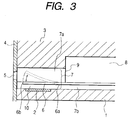
- Fig. 3 is a cross-sectional view taken along the direction of liquid flow path for explaining a basic structure of a liquid discharging head according to the present invention.
- the liquid discharging head comprises an element substrate 1 on which a plurality of heating elements 2 (only one of them are shown in Fig. 3) for imparting a bubble generating heat energy to liquid are provided in parallel, a top plate 3 connected to other member above this element substrate 1, and an orifice plate 4 connected to the front edges of the element substrate 1 and top plate 3.
- the element substrate 1 is formed by forming a silicon oxide film or silicon nitride film for insulation and heat accumulation on a substrate of, for example, silicon or the like, and forming a patterned electric resistance layer forming the heating element 2, and a patterned wiring, on the film.
- the heating element 2 is heated by applying the voltage on the electric resistance layer from this wiring and flowing current to the electric resistance layer.
- the top plate 3 is formed to form a plurality of liquid flow paths 7 corresponding to each of the heating elements 2 and a common liquid chamber 8 for supplying liquid to each of the liquid flow paths 7.
- a flow path side wall 9 extending between the heating elements from a ceiling portion is integrally provided with the top plate 3.
- the top plate 3 is composed of a silicon type material, and can be formed by etching the patterns of the liquid flow path 7 and common liquid chamber 8, or depositing a material of the flow path side wall 9, such as silicon nitride or silicon oxide etc., and etching the portion of the liquid flow path 7.
- the orifice plate 4 In the orifice plate 4 is formed a plurality of discharge ports 5, each of which is communicated with the common liquid chamber 8 through each of the liquid flow paths 7.
- the discharge port 5 corresponds to each of the liquid flow paths 7.
- the orifice plate 4 is also composed of silicon type material and can be formed, for example, by planing a silicon substrate provided with a discharge port 5 to about 10 to 150 ⁇ m.
- the orifice plate 4 is not always a required constitution in the present invention.
- a wall having substantially the same thickness as that of the orifice plate 4 is left in the top plate 3 and the discharge port 5 is formed in the wall portion, whereby a top plate with a discharge port can be formed.
- the liquid discharging head is provided with a cantilever type movable member 6 positioned opposingly to the heating element 2 so that the liquid flow path 7 is divided into a first liquid flow path 7a communicated with the discharge port 5 and a second liquid flow path 7b having the heating element 2.
- the movable member is a thin film composed of a silicon type material, such as silicon nitride, silicon oxide or the like.
- This movable member 6 is provided at a position facing the heating element 2 while having a desired distance from the heating element 2 and covering it.
- the movable member 6 has a fulcrum 6a on the upstream side of a large flow which flows from the common liquid chamber 8 to the discharge port side through the movable member 6 by the discharging action of liquid, and a free end 6b on the downstream side with respect to the fulcrum 6a.
- the space between this heating element 2 and movable member 6 becomes a bubble generation region 10.
- the heating element When the heating element is heated, based on the above-mentioned constitution, heat is acted on the liquid of the bubble generation region 10 between the movable member 6 and heating element 2, thereby generating bubbles on the heating element 2 due to the film boiling phenomena and being grown.
- the pressure generated by the growth of the bubbles is preferentially acted on the movable member 6.
- the movable member 6 is displaced so that it is greatly opened or pivoted on the discharge port 5 side keeping the fulcrum 6a as the center, as shown in Fig. 3 by a broken line.
- the bubble pressure propagation direction is led to the downstream side and the bubble pressure directly and efficiently contributes to the discharge of liquid.
- the bubble growth direction itself is also led to the downstream side as in the pressure propagation direction, whereby bubbles are further largely grown in the downstream than in the upstream.
- positioning a valve with a high precision can be realized by the photolithography steps and controlling of the valve thickness can be easily performed, whereby simplified steps can be realized.
- the ink jet head valve can be produced in a curved shape by the stress control of an underlying metal layer and the CVD stress control.
- a method of producing an ink jet head valve for an ink jet head having a discharge port for discharging ink, an ink flow path communicated with said discharge port and an electrothermal converting member used as an energy generating means for discharging ink into said ink flow path comprises the step of producing said ink jet head valve by a metal CVD process.
Abstract
Description
- The present invention relates to a method of producing an ink jet head valve, a method of producing an ink jet head and an ink jet head produced by the method.
- An ink jet recording process, so called a bubble jet recording process, in which a state change including a rapid volume change of ink (i.e., generation of bubbles) is caused to generate by imparting energy such as heat or the like to the ink, the ink is discharged from a discharge port by an active force due to this state change and the discharged ink is adhered to a medium to be recorded to perform an image formation, has been well known. In the recording device using this bubble jet recording process, as disclosed in publications of the specification of U.S. Patent No. 4,723,129 and the like, there are generally provided a discharge port for discharging ink, an ink flow path communicated with this discharge port and an electrothermal converting member used as an energy generating means for discharging ink provided in the ink flow path.
- According to such recording process, a high quality level image can be recorded at high speed and low noise and a discharge port for discharging ink can be provided at high density in a head in this recording process. Therefore, the recording process has a number of the advantages that a high revolution recording image and such color image could easily be obtained in a compact device. Thus, this bubble jet recording process has recently been used in various office equipment such as a printer, copy machine, facsimile and the like. Further, the recording process is used even in an industrial system such as a printing equipment etc.
- With the increased use of the bubble jet technology in products in many fields, the following various demands is recently increased.
- For example, an answer to demand of improvement of energy efficiency includes optimization of a heating element in which thickness of a protective film is controlled. This technology has an advantage in that the transmission efficiency of generated heat to liquid is enhanced.
- Further, to obtain a high definition image, there is provided a driving condition for imparting a liquid discharging method in which an improved ink discharge based on a stable bubble generation can be performed. Furthermore, to obtain a liquid discharge head having a high refilling speed of a discharged liquid to a liquid flow path from the viewpoint of the high speed recording, there is also provided a liquid discharge head having improved shapes of the liquid flow path.
- A flow path structure and a head producing method disclosed in Japanese Patent Laid-open Application No. 63-199972, relating to the shapes of the flow path, are inventions directed to a back wave (pressure in a direction opposite to that toward a discharge port, that is pressure toward a liquid chamber) which is generated with the generation bubbles. This back wave is known as a loss energy since it is not an energy toward the discharge direction.
- A head disclosed in the Japanese Patent Laid-open Application No. 63-199972, has an ink jet head valve which is spaced from a bubbling area of bubbles formed by the heating element and is positioned at the opposite side to the discharge port with respect to the heating element. This valve has an initial position in a manner that it is adhered to the ceiling of the flow path by a head producing method using a plate material, and is hung down in the flow path with the generation of bubbles. This application discloses an invention in which an energy loss is controlled by controlling a part of the above-mentioned back wave with a valve.
- Further, to realize improvements of liquid discharge properties including control of the back wave, and of liquid supply properties, the Japanese Patent Laid-open Application No. 9-201966 discloses a constitution in which a movable member is provided facing a bubble generation area which generates bubbles, and the growth of bubbles is controlled by using displacement of the movable member, generated by pressure at the time of bubble generation.
- Fig. 4 shows a partially broken perspective view of one embodiment of a liquid discharging head provided with such ink jet head valve.
- In the liquid discharging head in Fig. 4, a
heating element 2 which allows a heat energy to act on liquid is provided on anelement substrate 1 as a discharge energy generating element for discharging liquid.Liquid flow paths 7 are provided on thiselement substrate 1 correspondingly to theheating element 2. Theliquid flow paths 7 are communicated with adischarge port 5, and are also communicated with a commonliquid chamber 13 for supplying liquid to the plurality ofliquid flow paths 7, thereby receiving an amount of liquid corresponding to the liquid discharged from a discharge port, from this commonliquid chamber 13. - On the
element substrate 1 of thisliquid flow paths 7 is provided an ink jet head valve in which a 1 µm thick plate-shapedmovable member 6 having a flat surface portion, which is composed of an elastic material, such as a thin film resin, metal or the like, is provided like a cantilever beam. - In Fig. 4, when the
heating element 2 is heated, heat is acted on liquid in a bubble generation region between themovable member 6 and heating element, thereby generating bubbles based on the film boiling phenomena. The pressure and bubbles based on the generation of bubbles act on themovable member 6 and cause themember 6 to displace so that the member is largely opened on a liquid discharge side using afulcrum 6a as the center of rotation, whereby the pressure generated by generation of bubbles and the bubbles themselves can be led to the down stream side where thedischarge port 5 is provided. - To produce the above-mentioned ink jet head valve, a valve material produced by an electroforming process or the like was used to laminate the material on a substrate.
- When the valve material is laminated on the substrate, it is necessary to provide a space of about 1 to 20 µm between the movable member and heating element so as to sufficiently obtain effects of the movable member. Further, to laminate the valve material produced by the electroforming process or the like so that a space can be formed in the movable portions, it is necessary to form a pedestal portion on the substrate so that a valve is previously fixed onto the substrate.
- Further, to form the pedestal portion having for example 5 µm, which is merely the height of the space, and to prevent the pedestal portion from being corroded with ink, it is necessary to form the portion by an Au plating process or the like. To perform the Au plating, sputtering of Au and patterning thereof by the photolithography technology are needed.
- Further, it is necessary to provide an electroformed valve on a surface of the Au pedestal after the Au plating, make positioning of the valve and fix the valve by a stud bump process or the like. However, it is difficult to position the valve with high precision.
- Therefore, not only the thickness control of the valve and positioning of the valve were difficult, but also the production steps were extremely complicated.
- Accordingly, the objects of the present invention are to solve the above-mentioned problems and provide a method of producing an improved ink jet head valve, a method of producing an ink jet head, and an ink jet head produced by the method.
- The above-mentioned objects of the present invention can be attained by the following means.
- In accordance with the present invention, there is provided a method of producing an ink jet head valve for an ink jet head having a discharge port for discharging ink, an ink flow path communicated with said discharge port and an electrothermal converting member used as an energy generating means for discharging ink into said ink flow path, comprising the step of producing said ink jet head valve by a metal CVD process.
- In accordance with another aspect of the present invention, there is provided a method of producing an ink jet head having a discharge port for discharging ink, an ink flow path communicated with said discharge port and an electrothermal converting member used as an energy generating means for discharging ink into said ink flow path, comprising the step of:
- Preparing a substrate provided with said electrothermal converting member and having a conducting portion on the surface of said substrate;
- forming a first masking layer for forming a pedestal portion of a valve of said ink jet head on said substrate surface;
- etching a portion of said first masking layer, said portion being a portion where the pedestal portion of said valve is formed;
- forming said pedestal portion by the metal CVD process and forming a conducting layer on said pedestal portion and first masking layer;
- forming a second masking layer on said conducting layer and etching a portion of said second masking layer, said portion being a portion where a movable member is formed; and
- removing said first and second masking layers after forming said movable member on said conducting layer by the metal CVD process.
-
- In accordance with another aspect of the present invention, there is provided an ink jet head produced by the above-mentioned method.
- It is preferable that the ink jet head valve and ink jet head are produced by using Ta, W, Pt, Mo, Cr, Mn, Fe, Co, Ni, or Cu.
- Further, it is preferable that the conducting layer is formed by compression stress and said movable member is formed by tensile stress.
- According to the present invention, positioning of a high precision valve obtained by the photolithography steps can be realized and controlling of the valve thickness can be easily performed, whereby simplified steps can be realized.
-
- Figs. 1A, 1B, 1C, 1D and 1E are cross-sectional views showing the first half production steps of an ink jet head valve according to the present invention;
- Figs. 2F, 2G, 2H, 2I and 2J are cross-sectional views showing the last half production steps of an ink jet head valve according to the present invention;
- Fig. 3 is a cross-sectional view taken along the direction of liquid flow path for explaining a basic structure of a liquid discharging head according to the present invention;
- Fig. 4 is a partially broken perspective view of one embodiment of a liquid discharging head provided with an ink jet head valve; and
- Fig. 5 is a cross-sectional view of an ink jet head valve produced in Example 2.
-
- The present invention will be described in detail by examples hereinbelow.
- Figs. 1A to 1E and Figs. 2F to 2J are cross-sectional views showing the first half and last half production steps of an ink jet head valve according to the present invention, respectively.
- First, to form a pedestal of a valve on a substrate, an about 5 µm thick PSG film is formed on a Ta film used as an anti-cavitation film at a temperature of 350 °C by a plasma CVD process (Fig. 1A). Then, to perform patterning of the PSG film by the photolithography process, resist is spin-coated on the PSG film to form a resist film thereon. After that a predetermined portion of the resist layer is exposed and developed. In this case, as a film material for forming the pedestal of a valve, PSG was used. However, the material is not limited to PSG, other materials such as an inorganic material, for example, BPSG, or SiO or the like, or an organic material may be used, if such material is not changed in quality in a metal CVD process which will be described later. Then, the PSG film is etched by a buffered hydrogen fluoride to form a desired PSG film pattern (Fig. 1B). Then, an about 5 µm thick tungsten film is formed on the obtained substrate by a selective tungsten (W) CVD process using conditions of mixed gases and the mixing ratio of WF6/SiH4/H2 = 10/7/1000 sccm, pressure of 26.6 Pa, and temperature of 260 °C. The tungsten film is selectively formed only on an exposed Ta portion, thereby forming a pedestal of a valve (Fig. 1C).
- Although W is selected as the material of the pedestal of a valve, the material is not limited to W, Ta, Pt, Mo, Cr, Mn, Fe, Co, Ni, Cu, or the like may be used, if they have functions as the materials of the valve pedestal and the valve itself. Alternatively, the materials of the pedestal and valve may be varied according to functions.
- After that, on the obtained substrate is formed an 1000 angstrom thick Ni wiring layer by a sputtering process (Fig. 1D). The Ni wiring layer is used for forming a valve material using a metal CVD process. In this case, the wiring layer was formed with Pd. However, other metals may be used. Then, an about 5 µm thick PSG film is formed by a plasma CVD process (Fig. 1E. As the insulating film, a PSG film was used. However, the insulating material is not limited to PSG, other materials such as an inorganic material, for example, BPSG, or SiO or the like, or an organic material may be used, if such material is not changed in quality in a metal CVD process which will be described later. Then, the PSG film is etched by a buffered hydrogen fluoride (HF) to form a desired PSG film pattern (Fig. 2F).
- Then, an about 5 µm thick tungsten film is formed on the obtained substrate by a selective tungsten (W) CVD process using conditions of mixed gases and the mixing ratio of WF6/SiH4/H2 = 10/7/1000 sccm, pressure of 26.6 Pa, and temperature of 260 °C. The tungsten film is selectively formed only on an exposed Pd portion, thereby forming a valve (Fig. 2G).
- Then, the PSG film around the valve is removed by a buffered hydrogen fluoride (Fig. 2H). After that Ni wiring layer is removed by hydrogen peroxide solution (Fig. 2I). Finally, the exposed PSG film is removed by the buffered hydrogen fluoride to form a pedestal and valve (Fig. 2J).
- In steps shown in Figs. 1A to 1E and Figs. 2F to 2J in Example 1, if stresses of the underlying wiring layer and metal layer formed by a metal CVD process are controlled, a previously curved valve having a cross-sectional view of Fig. 5 not Fig. 2J, can be formed as the final configuration.
- For example, if an underlying wiring layer is formed by a compression stress of 1 × 10⁹ dyn/cm2 and the metal layer on the metal CVD side is formed by a tensile stress of 1 × 10⁹ dyn/cm2, the valve is deformed so that it is warped on the metal CVD side as shown in Fig. 5. Thus formed valve does not require power to deform the valve during bubbling and can be moved only at the time of refilling. Therefore, the valve can reduce lost energy.
- Fig. 3 is a cross-sectional view taken along the direction of liquid flow path for explaining a basic structure of a liquid discharging head according to the present invention.
- As shown in Fig. 3, the liquid discharging head comprises an
element substrate 1 on which a plurality of heating elements 2 (only one of them are shown in Fig. 3) for imparting a bubble generating heat energy to liquid are provided in parallel, atop plate 3 connected to other member above thiselement substrate 1, and an orifice plate 4 connected to the front edges of theelement substrate 1 andtop plate 3. - The
element substrate 1 is formed by forming a silicon oxide film or silicon nitride film for insulation and heat accumulation on a substrate of, for example, silicon or the like, and forming a patterned electric resistance layer forming theheating element 2, and a patterned wiring, on the film. Theheating element 2 is heated by applying the voltage on the electric resistance layer from this wiring and flowing current to the electric resistance layer. - The
top plate 3 is formed to form a plurality ofliquid flow paths 7 corresponding to each of theheating elements 2 and acommon liquid chamber 8 for supplying liquid to each of theliquid flow paths 7. A flowpath side wall 9 extending between the heating elements from a ceiling portion is integrally provided with thetop plate 3. Thetop plate 3 is composed of a silicon type material, and can be formed by etching the patterns of theliquid flow path 7 and commonliquid chamber 8, or depositing a material of the flowpath side wall 9, such as silicon nitride or silicon oxide etc., and etching the portion of theliquid flow path 7. - In the orifice plate 4 is formed a plurality of
discharge ports 5, each of which is communicated with thecommon liquid chamber 8 through each of theliquid flow paths 7. Thedischarge port 5 corresponds to each of theliquid flow paths 7. The orifice plate 4 is also composed of silicon type material and can be formed, for example, by planing a silicon substrate provided with adischarge port 5 to about 10 to 150 µm. The orifice plate 4 is not always a required constitution in the present invention. In place of provision of the orifice plate 4, when theliquid flow path 7 is formed in thetop plate 3, a wall having substantially the same thickness as that of the orifice plate 4 is left in thetop plate 3 and thedischarge port 5 is formed in the wall portion, whereby a top plate with a discharge port can be formed. - Further, the liquid discharging head is provided with a cantilever type
movable member 6 positioned opposingly to theheating element 2 so that theliquid flow path 7 is divided into a firstliquid flow path 7a communicated with thedischarge port 5 and a secondliquid flow path 7b having theheating element 2. The movable member is a thin film composed of a silicon type material, such as silicon nitride, silicon oxide or the like. - This
movable member 6 is provided at a position facing theheating element 2 while having a desired distance from theheating element 2 and covering it. Themovable member 6 has afulcrum 6a on the upstream side of a large flow which flows from thecommon liquid chamber 8 to the discharge port side through themovable member 6 by the discharging action of liquid, and afree end 6b on the downstream side with respect to thefulcrum 6a. The space between thisheating element 2 andmovable member 6 becomes abubble generation region 10. - When the heating element is heated, based on the above-mentioned constitution, heat is acted on the liquid of the
bubble generation region 10 between themovable member 6 andheating element 2, thereby generating bubbles on theheating element 2 due to the film boiling phenomena and being grown. The pressure generated by the growth of the bubbles is preferentially acted on themovable member 6. Themovable member 6 is displaced so that it is greatly opened or pivoted on thedischarge port 5 side keeping thefulcrum 6a as the center, as shown in Fig. 3 by a broken line. By the displacement of themovable member 6 or the state of the displaced thereof, propagation of pressure due to the generation of bubbles and grown bubbles themselves are led to thedischarge port 5 side, whereby liquid is discharged from thedischarge port 5. - Namely, by providing the
movable member 6 having thefulcrum 6a on the upstream side (commonliquid chamber 8 side) of the liquid flow in theliquid flow path 7 and thefree end 6b on the downstream side (dischargeport 5 side), on thebubble generation region 10, the bubble pressure propagation direction is led to the downstream side and the bubble pressure directly and efficiently contributes to the discharge of liquid. Further, the bubble growth direction itself is also led to the downstream side as in the pressure propagation direction, whereby bubbles are further largely grown in the downstream than in the upstream. Thus, by controlling the bubble growth direction itself with the movable member and controlling the bubble pressure propagation direction, fundamental discharge properties such as discharge efficiency, discharge output, or discharge speed etc., can be improved. - On the other hand, when bubbles are in a bubble vanishing step, the bubbles are rapidly vanished by a multiplier effect of elasticity of the
movable member 6 and themovable member 6 is finally returned to the original position as shown in Fig. 3 by a solid line. In this case, to compensate the shrinkage volume of bubbles in thebubble generation region 10 and to compensate the amount for the volume of discharged liquid, liquid is flown from the upstream side, that is thecommon liquid chamber 8 side to refill liquid into theliquid flow path 7. This refilling of the liquid can be efficiently, reasonably and stably performed by the return action of themovable member 6. - According to the present invention, positioning a valve with a high precision can be realized by the photolithography steps and controlling of the valve thickness can be easily performed, whereby simplified steps can be realized.
- Further, according to the present invention, the ink jet head valve can be produced in a curved shape by the stress control of an underlying metal layer and the CVD stress control.
- A method of producing an ink jet head valve for an ink jet head having a discharge port for discharging ink, an ink flow path communicated with said discharge port and an electrothermal converting member used as an energy generating means for discharging ink into said ink flow path, comprises the step of producing said ink jet head valve by a metal CVD process.
Claims (6)
- A method of producing an ink jet head valve for an ink jet head having a discharge port for discharging ink, an ink flow path communicated with said discharge port and an electrothermal converting member used as an energy generating means for discharging ink into said ink flow path, comprising the step of producing said ink jet head valve by a metal CVD process.
- A method of producing an ink jet head valve according to claim 1, wherein said ink jet head valve is produced by using Ta, W, Pt, Mo, Cr, Mn, Fe, Co, Ni, or Cu.
- A method of producing an ink jet head having a discharge port for discharging ink, an ink flow path communicated with said discharge port and an electrothermal converting member used as an energy generating means for discharging ink into said ink flow path, comprising the steps of:preparing a substrate provided with said electrothermal converting member and having a conducting portion on the surface of said substrate;forming a first masking layer for forming a pedestal portion of a valve of said ink jet head on said substrate surface;etching a portion of said first masking layer, said portion being a portion where the pedestal portion of said valve is formed;forming said pedestal portion by the metal CVD process and forming a conducting layer on said pedestal portion and first masking layer;forming a second masking layer on said conducting layer and etching a portion of said second masking layer, said portion being a portion where a movable member is formed; andremoving said first and second masking layers after forming said movable member on said conducting layer by the metal CVD process.
- A method of producing an ink jet head according to claim 3, wherein said ink jet head valve is produced by using Ta, W, Pt, Mo, Cr, Mn, Fe, Co, Ni, or Cu.
- A method of producing an ink jet head according to claim 3, wherein said conducting layer is formed by compression stress and said movable member is formed by tensile stress.
- An ink jet head produced by the method according to claims 3 to 5.
Applications Claiming Priority (2)
| Application Number | Priority Date | Filing Date | Title |
|---|---|---|---|
| JP33605997 | 1997-12-05 | ||
| JP33605997A JP3530732B2 (en) | 1997-12-05 | 1997-12-05 | Method of manufacturing inkjet head |
Publications (3)
| Publication Number | Publication Date |
|---|---|
| EP0920995A2 true EP0920995A2 (en) | 1999-06-09 |
| EP0920995A3 EP0920995A3 (en) | 2000-02-23 |
| EP0920995B1 EP0920995B1 (en) | 2003-03-19 |
Family
ID=18295280
Family Applications (1)
| Application Number | Title | Priority Date | Filing Date |
|---|---|---|---|
| EP98122941A Expired - Lifetime EP0920995B1 (en) | 1997-12-05 | 1998-12-03 | Method of producing ink jet head valve, method of producing ink jet head and ink jet head produced by the method |
Country Status (4)
| Country | Link |
|---|---|
| US (1) | US6277294B1 (en) |
| EP (1) | EP0920995B1 (en) |
| JP (1) | JP3530732B2 (en) |
| DE (1) | DE69812282T2 (en) |
Cited By (1)
| Publication number | Priority date | Publication date | Assignee | Title |
|---|---|---|---|---|
| EP1715999A1 (en) * | 2004-02-09 | 2006-11-02 | Ricoh Company, Ltd. | Liquid ejection head, liquid cartridge, liquid ejection apparatus, image forming apparatus and manufacturing method of liquid ejecting head |
Families Citing this family (5)
| Publication number | Priority date | Publication date | Assignee | Title |
|---|---|---|---|---|
| JP2004107181A (en) * | 2002-09-20 | 2004-04-08 | Canon Inc | Composition for forming piezoelectric element, method of manufacturing piezoelectric film, piezoelectric element and inkjet recording head |
| TWI230477B (en) * | 2002-09-20 | 2005-04-01 | Canon Kk | Composition for forming piezoelectric film, producing method for piezoelectric film, piezoelectric element and ink jet recording head |
| JP2004107179A (en) | 2002-09-20 | 2004-04-08 | Canon Inc | Precursor sol of piezoelectric material, method of manufacturing piezoelectric film, piezoelectric element, and inkjet recording head |
| JP3971279B2 (en) * | 2002-09-20 | 2007-09-05 | キヤノン株式会社 | Method for manufacturing piezoelectric element |
| JP5501167B2 (en) | 2010-09-08 | 2014-05-21 | キヤノン株式会社 | Inkjet head manufacturing method |
Citations (2)
| Publication number | Priority date | Publication date | Assignee | Title |
|---|---|---|---|---|
| US4723129A (en) | 1977-10-03 | 1988-02-02 | Canon Kabushiki Kaisha | Bubble jet recording method and apparatus in which a heating element generates bubbles in a liquid flow path to project droplets |
| JPS63199972A (en) | 1987-02-13 | 1988-08-18 | Canon Inc | Manufacture of valve element |
Family Cites Families (6)
| Publication number | Priority date | Publication date | Assignee | Title |
|---|---|---|---|---|
| JPS63197652A (en) | 1987-02-13 | 1988-08-16 | Canon Inc | Ink jet recording head and its preparation |
| JPH05131636A (en) | 1991-11-11 | 1993-05-28 | Canon Inc | Liquid jet recording head and production thereof |
| US5278585A (en) | 1992-05-28 | 1994-01-11 | Xerox Corporation | Ink jet printhead with ink flow directing valves |
| JP3342279B2 (en) | 1995-01-13 | 2002-11-05 | キヤノン株式会社 | Liquid discharge method, liquid discharge head, and method of manufacturing the liquid discharge head |
| ATE235375T1 (en) | 1995-04-26 | 2003-04-15 | Canon Kk | LIQUID DISCHARGE HEAD, LIQUID DISCHARGE DEVICE AND LIQUID DISCHARGE METHOD |
| JP3524340B2 (en) | 1997-08-26 | 2004-05-10 | キヤノン株式会社 | Liquid ejection head |
-
1997
- 1997-12-05 JP JP33605997A patent/JP3530732B2/en not_active Expired - Fee Related
-
1998
- 1998-12-02 US US09/203,393 patent/US6277294B1/en not_active Expired - Lifetime
- 1998-12-03 DE DE69812282T patent/DE69812282T2/en not_active Expired - Lifetime
- 1998-12-03 EP EP98122941A patent/EP0920995B1/en not_active Expired - Lifetime
Patent Citations (2)
| Publication number | Priority date | Publication date | Assignee | Title |
|---|---|---|---|---|
| US4723129A (en) | 1977-10-03 | 1988-02-02 | Canon Kabushiki Kaisha | Bubble jet recording method and apparatus in which a heating element generates bubbles in a liquid flow path to project droplets |
| JPS63199972A (en) | 1987-02-13 | 1988-08-18 | Canon Inc | Manufacture of valve element |
Cited By (2)
| Publication number | Priority date | Publication date | Assignee | Title |
|---|---|---|---|---|
| EP1715999A1 (en) * | 2004-02-09 | 2006-11-02 | Ricoh Company, Ltd. | Liquid ejection head, liquid cartridge, liquid ejection apparatus, image forming apparatus and manufacturing method of liquid ejecting head |
| EP1715999A4 (en) * | 2004-02-09 | 2008-07-02 | Ricoh Kk | Liquid ejection head, liquid cartridge, liquid ejection apparatus, image forming apparatus and manufacturing method of liquid ejecting head |
Also Published As
| Publication number | Publication date |
|---|---|
| EP0920995A3 (en) | 2000-02-23 |
| JPH11170546A (en) | 1999-06-29 |
| JP3530732B2 (en) | 2004-05-24 |
| DE69812282D1 (en) | 2003-04-24 |
| EP0920995B1 (en) | 2003-03-19 |
| US6277294B1 (en) | 2001-08-21 |
| DE69812282T2 (en) | 2004-01-22 |
Similar Documents
| Publication | Publication Date | Title |
|---|---|---|
| Chen et al. | A high-resolution silicon monolithic nozzle array for inkjet printing | |
| US6834943B2 (en) | Liquid discharge head, a substrate for use of such head and a method of manufacture therefor | |
| US4459600A (en) | Liquid jet recording device | |
| JPS63197652A (en) | Ink jet recording head and its preparation | |
| KR100435012B1 (en) | Ink jet head substrate, ink jet head, method for manufacturing ink jet head substrate, method for manufacturing ink jet head, method for using ink jet head and ink jet recording apparatus | |
| EP0888888A2 (en) | A magnetically actuated ink jet printing device | |
| US7250113B2 (en) | Method for manufacturing liquid ejection head | |
| EP0920995B1 (en) | Method of producing ink jet head valve, method of producing ink jet head and ink jet head produced by the method | |
| US6386686B1 (en) | Liquid discharge head, manufacturing method of liquid discharge head, head cartridge, and liquid discharge apparatus | |
| US6196667B1 (en) | Liquid discharging head, method of manufacturing the liquid discharging head, head cartridge carrying the liquid discharging head thereon and liquid discharging apparatus | |
| US5708466A (en) | Ink jet head having parallel liquid paths and pressure-directing wall | |
| JP3524340B2 (en) | Liquid ejection head | |
| US6431687B1 (en) | Manufacturing method of monolithic integrated thermal bubble inkjet print heads and the structure for the same | |
| JP3697255B2 (en) | Method for manufacturing inkjet head valve | |
| JP3533205B2 (en) | Micro droplet generating apparatus and method for manufacturing the same | |
| EP1005992B1 (en) | Substrate for liquid discharge head, liquid discharge head and liquid discharge apparatus | |
| JP3554149B2 (en) | Manufacturing method of liquid ejection head | |
| JP3125536B2 (en) | Inkjet head | |
| US20030038852A1 (en) | Liquid discharge head liquid discharge method and liquid discharge apparatus | |
| JP2003118114A (en) | Ink jet head and its manufacturing method | |
| JP3639707B2 (en) | Liquid discharge head and head substrate | |
| KR20010066812A (en) | Manufacturing method of ink jet printer head | |
| JPH1148488A (en) | Liquid jet head and manufacture thereof | |
| JP3672559B2 (en) | Ink jet recording head chip manufacturing method, ink jet recording head manufacturing method, and recording apparatus | |
| JPH1148500A (en) | Liquid jet head, manufacture thereof and movable member therefor |
Legal Events
| Date | Code | Title | Description |
|---|---|---|---|
| PUAI | Public reference made under article 153(3) epc to a published international application that has entered the european phase |
Free format text: ORIGINAL CODE: 0009012 |
|
| AK | Designated contracting states |
Kind code of ref document: A2 Designated state(s): CH DE ES FR GB IT LI NL SE |
|
| AX | Request for extension of the european patent |
Free format text: AL;LT;LV;MK;RO;SI |
|
| PUAL | Search report despatched |
Free format text: ORIGINAL CODE: 0009013 |
|
| AK | Designated contracting states |
Kind code of ref document: A3 Designated state(s): AT BE CH CY DE DK ES FI FR GB GR IE IT LI LU MC NL PT SE |
|
| AX | Request for extension of the european patent |
Free format text: AL;LT;LV;MK;RO;SI |
|
| 17P | Request for examination filed |
Effective date: 20000706 |
|
| AKX | Designation fees paid |
Free format text: CH DE ES FR GB IT LI NL SE |
|
| 17Q | First examination report despatched |
Effective date: 20010129 |
|
| GRAG | Despatch of communication of intention to grant |
Free format text: ORIGINAL CODE: EPIDOS AGRA |
|
| GRAG | Despatch of communication of intention to grant |
Free format text: ORIGINAL CODE: EPIDOS AGRA |
|
| GRAH | Despatch of communication of intention to grant a patent |
Free format text: ORIGINAL CODE: EPIDOS IGRA |
|
| GRAH | Despatch of communication of intention to grant a patent |
Free format text: ORIGINAL CODE: EPIDOS IGRA |
|
| GRAA | (expected) grant |
Free format text: ORIGINAL CODE: 0009210 |
|
| AK | Designated contracting states |
Designated state(s): CH DE ES FR GB IT LI NL SE |
|
| PG25 | Lapsed in a contracting state [announced via postgrant information from national office to epo] |
Ref country code: NL Free format text: LAPSE BECAUSE OF FAILURE TO SUBMIT A TRANSLATION OF THE DESCRIPTION OR TO PAY THE FEE WITHIN THE PRESCRIBED TIME-LIMIT Effective date: 20030319 Ref country code: LI Free format text: LAPSE BECAUSE OF FAILURE TO SUBMIT A TRANSLATION OF THE DESCRIPTION OR TO PAY THE FEE WITHIN THE PRESCRIBED TIME-LIMIT Effective date: 20030319 Ref country code: CH Free format text: LAPSE BECAUSE OF FAILURE TO SUBMIT A TRANSLATION OF THE DESCRIPTION OR TO PAY THE FEE WITHIN THE PRESCRIBED TIME-LIMIT Effective date: 20030319 |
|
| REG | Reference to a national code |
Ref country code: GB Ref legal event code: FG4D |
|
| REG | Reference to a national code |
Ref country code: CH Ref legal event code: EP |
|
| REF | Corresponds to: |
Ref document number: 69812282 Country of ref document: DE Date of ref document: 20030424 Kind code of ref document: P |
|
| PG25 | Lapsed in a contracting state [announced via postgrant information from national office to epo] |
Ref country code: SE Free format text: LAPSE BECAUSE OF FAILURE TO SUBMIT A TRANSLATION OF THE DESCRIPTION OR TO PAY THE FEE WITHIN THE PRESCRIBED TIME-LIMIT Effective date: 20030619 |
|
| NLV1 | Nl: lapsed or annulled due to failure to fulfill the requirements of art. 29p and 29m of the patents act | ||
| PG25 | Lapsed in a contracting state [announced via postgrant information from national office to epo] |
Ref country code: ES Free format text: LAPSE BECAUSE OF FAILURE TO SUBMIT A TRANSLATION OF THE DESCRIPTION OR TO PAY THE FEE WITHIN THE PRESCRIBED TIME-LIMIT Effective date: 20030930 |
|
| REG | Reference to a national code |
Ref country code: CH Ref legal event code: PL |
|
| ET | Fr: translation filed | ||
| PLBE | No opposition filed within time limit |
Free format text: ORIGINAL CODE: 0009261 |
|
| STAA | Information on the status of an ep patent application or granted ep patent |
Free format text: STATUS: NO OPPOSITION FILED WITHIN TIME LIMIT |
|
| 26N | No opposition filed |
Effective date: 20031222 |
|
| PGFP | Annual fee paid to national office [announced via postgrant information from national office to epo] |
Ref country code: FR Payment date: 20061208 Year of fee payment: 9 |
|
| PGFP | Annual fee paid to national office [announced via postgrant information from national office to epo] |
Ref country code: IT Payment date: 20061231 Year of fee payment: 9 |
|
| REG | Reference to a national code |
Ref country code: FR Ref legal event code: ST Effective date: 20081020 |
|
| PG25 | Lapsed in a contracting state [announced via postgrant information from national office to epo] |
Ref country code: FR Free format text: LAPSE BECAUSE OF NON-PAYMENT OF DUE FEES Effective date: 20071231 |
|
| PG25 | Lapsed in a contracting state [announced via postgrant information from national office to epo] |
Ref country code: IT Free format text: LAPSE BECAUSE OF NON-PAYMENT OF DUE FEES Effective date: 20071203 |
|
| PGFP | Annual fee paid to national office [announced via postgrant information from national office to epo] |
Ref country code: DE Payment date: 20141231 Year of fee payment: 17 Ref country code: GB Payment date: 20141222 Year of fee payment: 17 |
|
| REG | Reference to a national code |
Ref country code: DE Ref legal event code: R119 Ref document number: 69812282 Country of ref document: DE |
|
| GBPC | Gb: european patent ceased through non-payment of renewal fee |
Effective date: 20151203 |
|
| PG25 | Lapsed in a contracting state [announced via postgrant information from national office to epo] |
Ref country code: GB Free format text: LAPSE BECAUSE OF NON-PAYMENT OF DUE FEES Effective date: 20151203 Ref country code: DE Free format text: LAPSE BECAUSE OF NON-PAYMENT OF DUE FEES Effective date: 20160701 |