EP0909035B1 - Phase synchronisation device and phase quadrature signal generating apparatus - Google Patents
Phase synchronisation device and phase quadrature signal generating apparatus Download PDFInfo
- Publication number
- EP0909035B1 EP0909035B1 EP98308210A EP98308210A EP0909035B1 EP 0909035 B1 EP0909035 B1 EP 0909035B1 EP 98308210 A EP98308210 A EP 98308210A EP 98308210 A EP98308210 A EP 98308210A EP 0909035 B1 EP0909035 B1 EP 0909035B1
- Authority
- EP
- European Patent Office
- Prior art keywords
- signal
- phase
- signals
- output
- reference signals
- Prior art date
- Legal status (The legal status is an assumption and is not a legal conclusion. Google has not performed a legal analysis and makes no representation as to the accuracy of the status listed.)
- Expired - Lifetime
Links
Images


Classifications
-
- H—ELECTRICITY
- H03—ELECTRONIC CIRCUITRY
- H03B—GENERATION OF OSCILLATIONS, DIRECTLY OR BY FREQUENCY-CHANGING, BY CIRCUITS EMPLOYING ACTIVE ELEMENTS WHICH OPERATE IN A NON-SWITCHING MANNER; GENERATION OF NOISE BY SUCH CIRCUITS
- H03B28/00—Generation of oscillations by methods not covered by groups H03B5/00 - H03B27/00, including modification of the waveform to produce sinusoidal oscillations
-
- H—ELECTRICITY
- H03—ELECTRONIC CIRCUITRY
- H03L—AUTOMATIC CONTROL, STARTING, SYNCHRONISATION, OR STABILISATION OF GENERATORS OF ELECTRONIC OSCILLATIONS OR PULSES
- H03L7/00—Automatic control of frequency or phase; Synchronisation
- H03L7/06—Automatic control of frequency or phase; Synchronisation using a reference signal applied to a frequency- or phase-locked loop
- H03L7/08—Details of the phase-locked loop
- H03L7/085—Details of the phase-locked loop concerning mainly the frequency- or phase-detection arrangement including the filtering or amplification of its output signal
- H03L7/093—Details of the phase-locked loop concerning mainly the frequency- or phase-detection arrangement including the filtering or amplification of its output signal using special filtering or amplification characteristics in the loop
-
- H—ELECTRICITY
- H03—ELECTRONIC CIRCUITRY
- H03L—AUTOMATIC CONTROL, STARTING, SYNCHRONISATION, OR STABILISATION OF GENERATORS OF ELECTRONIC OSCILLATIONS OR PULSES
- H03L7/00—Automatic control of frequency or phase; Synchronisation
- H03L7/06—Automatic control of frequency or phase; Synchronisation using a reference signal applied to a frequency- or phase-locked loop
- H03L7/08—Details of the phase-locked loop
- H03L7/099—Details of the phase-locked loop concerning mainly the controlled oscillator of the loop
- H03L7/0995—Details of the phase-locked loop concerning mainly the controlled oscillator of the loop the oscillator comprising a ring oscillator
- H03L7/0998—Details of the phase-locked loop concerning mainly the controlled oscillator of the loop the oscillator comprising a ring oscillator using phase interpolation
-
- H—ELECTRICITY
- H04—ELECTRIC COMMUNICATION TECHNIQUE
- H04L—TRANSMISSION OF DIGITAL INFORMATION, e.g. TELEGRAPHIC COMMUNICATION
- H04L7/00—Arrangements for synchronising receiver with transmitter
- H04L7/02—Speed or phase control by the received code signals, the signals containing no special synchronisation information
- H04L7/033—Speed or phase control by the received code signals, the signals containing no special synchronisation information using the transitions of the received signal to control the phase of the synchronising-signal-generating means, e.g. using a phase-locked loop
-
- H—ELECTRICITY
- H04—ELECTRIC COMMUNICATION TECHNIQUE
- H04L—TRANSMISSION OF DIGITAL INFORMATION, e.g. TELEGRAPHIC COMMUNICATION
- H04L7/00—Arrangements for synchronising receiver with transmitter
- H04L7/0016—Arrangements for synchronising receiver with transmitter correction of synchronization errors
- H04L7/002—Arrangements for synchronising receiver with transmitter correction of synchronization errors correction by interpolation
- H04L7/0025—Arrangements for synchronising receiver with transmitter correction of synchronization errors correction by interpolation interpolation of clock signal
Definitions
- the present invention relates to devices for synchronising an output signal with an input signal, and in particular to devices which use interpolation or mixing of two reference sources to generate the output.
- Phase locked loops are well known electronic devices and they function to provide an output oscillating signal which is phase locked with an incoming signal.
- the output signal is generated by a voltage controlled oscillator (VCO) and this output is compared by a phase detector with the input signal. This produces an error signal representing the phase difference between the input and the output and this error is applied, typically via an appropriate filter, to alter the control voltage of the VCO.
- the oscillating frequency of the VCO is therefore altered until such time as the output is in phase with the input at which time no further error signal is generated and no further changes are made to the control voltage input to the VCO.
- PLLs are typically used where it is desired to generate a clean clock signal synchronised with an incoming signal.
- One particular application of PLLs is in data transmission systems, for instance communication devices where the transmitted signal is modulated based on a signal having a particular frequency and it is important to recover a corresponding clock signal at the receiver in order to demodulate the received signal.
- PLLs in close proximity. For instance there may be PLLs both in the transmit side of the system and in the receive side, and also in a multi-channel system there may be a PLL for each of the channels. If such arrangements are implemented on a single chip problems can occur due to interference between VCOs implemented in such close proximity. Also as data rates increase, the power consumption of the VCO required to generate a satisfactorily low-noise signal increases and this is compounded if more than one VCO is implemented in any particular device.
- clock signals may be used in a number of parts of any specific electronic circuitry.
- clock signals are carried around a chip or circuit board arrangement by suitable conductive means so as to be transferred from the clock generator to the part of the circuitry dependent on the clock.
- the present invention provides an apparatus for generating an oscillating output signal as set forth in the claims.
- the present invention does not require the presence of a voltage controlled oscillator or other clock source implemented as part of a PLL. Rather it depends on the availability of two or more externally generated reference signals, such as may be available elsewhere in the circuitry as mentioned above.
- the receiver PLL may be according to this invention and may derive its reference signals from the VCO output in the transmitter side PLL. This removes the possibility of damaging interference between two VCOs on the same chip and also reduces the overall power requirement.
- both the transmitter and receiver PLLs may receive input clock reference signals from elsewhere.
- This invention is particularly suited to situations such as those referred to above in the communications field where the frequency of the desired output is fairly accurately known as in this case the reference signals would be set to have approximately this frequency. However it is possible and potentially useful within the present invention to generate an output signal having a frequency different from the frequency of the reference signals, and therefore synchronise with an input signal of a different frequency.
- the comparison between the input and the output signal in the invention is broadly the same as the prior art, that is a signal is generated according to phase comparison between the input and the output signals. In the invention this is used to derive and constantly correct the weightings used in the mixing of the reference signals.
- the two references may be arranged non-orthogonal, in which case the relationships between the derived phase relationships and the weighting values is different but can be easily derived. Also it is possible to use three or more references at equal or non-equal phase spacings with appropriate weighting values.
- Quadrature related signals are advantageously used as the reference signals in the PLL, and as will be explained in more detail below a multi-channel communications arrangement can be easily implemented with only one source of clock signals and means arranged to regenerate the quadrature relationship between the clock signals at appropriate points.
- the invention is apparatus for producing an oscillating signal in a predetermined phase relationship with an input signal which generates its output signal by mixing in variable proportions two or more reference oscillating signals.
- the reference signals should be in quadrature relationship and have approximately the same frequency as the desired output, but this is not essential.
- the output signal may be desired to be in phase with the input signal or to have a predetermined phase offset.
- apparatus is described which generates quadrature related clock signals, which may be used as the reference signals in the phase-lock arrangement.
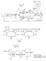
- FIG. 1 illustrates in schematic form a schematic diagram of a prior art PLL the operation of which is useful to understand for the understanding of the present invention.
- the PLL illustration in Figure 1 comprises a voltage controlled oscillator (VCO) 10 which has a control voltage applied to it and which outputs a clock signal 12.
- VCO voltage controlled oscillator
- the frequency of the output 12 is a function of the magnitude of the control voltage enabling the frequency of output 12 to be controlled by varying the control voltage.
- the PLL has input to it a signal 14, for instance a data signal based on a remotely derived clock signal, and it is desired that clock signal 12 should be synchronised with input signal 14.
- phase detector 16 which compares the phases of the two signals in order to generate a signal 18 according to the phase difference between signals 12 and 14.
- signal 18 indicates whether the frequency of output signal 12 needs to increase or decrease in order to bring signals 12 and 14 more in phase with each other.
- the illustrated PLL comprises filter 19 (which may essentially be integrating signal 18) which provides the control voltage for VCO 10 such that the control voltage increases and decreases according to signal 18.
- a PLL is therefore essentially a closed loop control system which compares the input and the output and controls the generation of the output according to the result of that comparison.
- Figure 2 illustrates in general terms the operation of the preferred embodiments of the present invention.
- the same reference numerals as were used in Figure 1 are used in Figure 2 for corresponding components.
- the device in Figure 2 has input thereto signal 14 and it is arranged to generate output signal 12 which is intended to have a particular phase relationship with the input signal 14.
- signal 12 is intended to be in phase with input signal 14, but it will be apparent that simple alterations can be made to the parameters of operation to achieve any desired phase relationship.
- signals 12 and 14 are compared in phase detector 16 which provides output 18 indicating whether the frequency of signal 12 needs to be increased or decreased to bring it more in phase with signal 14.
- signal 12 is not generated as the output of a voltage control oscillator. Rather, it is the output of the mixing means 20.
- Mixing means 20 has input to it two reference signals or clock sources CLK1 and CLK2. Signals CLK1 and CLK2 have the same frequencies as each other but are out of phase, and in the particularly preferred embodiment these two signals are 90° out of phase as illustrated in the phasor diagram in Figure 3a.
- Mixing means 20 mixes signals CLK1 and CLK2 in variable proportions in accordance with output 18 from phase detector 16 in order to generate output 12. The proportions in which the signals CLK1 and CLK2 are mixed together vary sinusoidally between -1 and +1 as described in more detail below in order that output signal 12 may have any phase relationship with the reference clock signals.
- FIG. 3b illustrates the weighting given to reference signal CLK1 and that given to signal CLK2 in designated W2.
- Figure 3b illustrates the values taken by W1 and W2 in order to generate various phase differences P as compared to reference signal CLK1, with 150° again shown as an example.
- the reference signals CLK1 and CLK2 may be derived from signals generated in the transmit side VCO, but the reference signals may be derived from any suitable source.
- FIG. 4 illustrates one embodiment in which the above sin and cos values are determined using look-up tables.
- mixing means 20 comprises digital filter 122 which generates value P according to signal 18 output by phase detector 16.
- the reference clock signals are designated ⁇ 1 and ⁇ 2 and are illustrated, by way of example as being received from a VCO forming part of another PLL. Any other suitable source of clock signals could however be utilised.
- Value P represents the desired phase difference between reference signal ⁇ 1 and output signal 12 in order to keep signal 12 in synchronisation with input signal 14.
- signal 18 will not indicate that any increase or decrease in frequency is required to bring the signals into phase, and therefore in such a state digital filter 122 outputs a constant value of P to maintain the established phase relationships. (A slightly different situation occurs if the input signal has a different frequency to the reference signals as discussed below).
- the desired value of W1 is cos P and the desired value of W2 is sin P.
- two look up tables 124a and 124b to which P is applied and which output, in digital form, the cosine and sine of P respectively.
- These signals are passed through digital to analogue converters 126a and 126b respectively in order to provide analogue signals W1 and W2 for input to phase interpolator 120.
- Phase interpolator 120 mixes ⁇ 1 and ⁇ 2 in the proportions determined by W1 and W2 to generate output signal 12.
- Figure 5 illustrates one possible implementation of phase interpolator 120 based on differential MOS circuit techniques in which each signal in Figure 4 is illustrated by two signals in Figure 5 having corresponding names with a and b suffixes.
- the implementation illustrated in Figure 5 enables W1 and W2 to vary over the complete range -1 to +1 enabling phase interpolator 120 to fully implement the functions discussed above.
- Digital filter 122 illustrated in Figure 4 may simply be an up/down counter. This would count up or down according to the polarity of input signal 18 until the desired value of P is being output at which time signal 18 would go to 0 and the value of P would remain constant at its desired locked value.
- the counter should be arranged to wrap around, when incrementing above the maximum count or decrementing below 0 in order to provide a fully functional device.
- Figure 6 illustrates an alternative implementation of digital filter 122 which overcomes this problem.
- Digital filter 122 as illustrated in Figure 6 comprises a counter 50, a multiplier 52 and an accumulator 54.
- the signal 18 indicating whether the phase of output signal 12 needs to be increased or decreased in order to achieve synchronism is input both to counter 50 and to accumulator 54.
- Counter 50 counts up or down according to the value of signal 18 to produce signal F which is multiplied by a constant K in multiplier 52 and is also input to accumulator 54.
- Accumulator 54 generates a new output value of P by adding, to the existing value of P, the two inputs it receives.
- Counter 50 in this implementation effectively integrates the increment/ decrement pulses of signal 18 so as to produce the value F.
- Value F therefore represents the frequency offset between the frequency of the reference signals and desired frequency for signal 12.
- this frequency difference is equivalent to a constantly changing phase difference and therefore this can be accounted for by constantly changing the value of P to track this phase difference.
- K of multiplier 52 and the addition of the multiplied signal into accumulator 54 is to cause signal P to track at the necessary rate of change of phase so as to synchronise with the different frequency signal.
- the signal 18 is also input directly to accumulator 54 so that when the system is not in the locked condition it will lock in properly and provide a stable system.
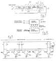
- FIG. 7 illustrates a particularly preferred implementation of the invention, the details of which are illustrated in the succeeding figures. It will be seen that the principles behind the implementation are similar to those outlined above, but the actual circuits used are different and, in certain circumstances, more practical.
- mixing means 20 comprises a digital control means 210 and phase interpolator 220, and the embodiment is described in terms of clock memory based on a serial data input.
- a standard phase detector circuit 16 is used to compare the positions of the edges in the serial data input 14 with the phase of the data recovery clock 12. This produces phase increment/decrement control signals which are fed into digital logic block 210 which generates a control word representing the required phase of the data recovery clock. The digital phase select value is then applied to the phase interpolator 220 which uses an analogue mixer to derive the required data recovery clock phase from the two reference clock phases.
- An optional reference regeneration circuit may be included to restore the quadrature phase relationship between the reference clock phases, thus allowing the effects of skew due to distribution of the clocks to be reduced. Details of this regeneration circuit are set out below.
- the phase interpolator 220 in this embodiment is formed of an analogue phase mixer 222 and a digitally controlled current source block 226.
- the current source block 226 provides current signals to the phase mixer 222 to provide, as discussed in more detail below, the weightings in which the reference signals CLK1 and CLK2 should be mixed.
- FIG. 9 A schematic illustration of an implementation of the phase mixer 222 based on differential techniques, in which each signal is represented by a pair of signal lines, is shown in Figure 9.
- the required weightings for the reference signals are provided by the current source block 226 as currents I1+, I1-, I2+, I2- which appear as current sources in Figure 9.
- the circuit of Figure 9 sums the reference clock signals according to the weights of their control currents to generate a Sum signal represented by the differential voltage developed across load resistors R1 and R2.
- the load capacitances (C1 and C2) are optional and may be included to filter out harmonics of the clock signals to reduce distortion of the Sum signal.
- the described operation assumes the use of sinusoidal reference clock signals. However, square clocks may also be used but require filtering either by C1 and C2, and/or by the intrinsic bandwidth limit of the phase summing circuit.
- Phase mixer 222 comprises four differential amplifiers 91a, 91b, 92a, 92b each of which includes two transistors as illustrated in a conventional fashion.
- Reference clock CLK1 is applied as shown to amplifiers 91a and 91b with opposite polarities.
- the provision of two amplifiers connected with opposite polarities means that one acts to add the reference clock to the Sum signal, while the other subtracts it.
- the current sources I1+, I1- control the relative extents to which the amplifiers add and subtract the reference signal, and thus the current pair I1+ and I1- constitute a differential current weighting representing W1 in Figure 3 above enabling W1 to be adjusted from +1 to -1.
- the weightings W1, W2 for the reference clocks CLK1, CLK2 can be varied as discussed above in relation to Figure 3 such that the phase of the Sum signal can be varied over a whole cycle.
- Sum signal is buffered using a second differential amplifier stage 94 to "square up" the signal and remove any amplitude variation resulting from the phase mixing operation to generate the second clock signal 12.
- the digital control value is encoded using a Johnson (twisted-ring) counter type code.
- This uses an N-bit word, PS[1:N], (where N is an even integer) to define 2N possible code values which are used to designate 2N available phase steps which may be output by the interpolator.
- N therefore effectively determines the phase resolution of the clock alignment circuitry: since there are 2N phase steps over one complete cycle (2 ⁇ radians), the phase resolution is ⁇ /N radians.
- the value of N is therefore chosen to trade off phase resolution with complexity.
- the 12 possible code values for a 6-bit implementation of the phase select are as follows: Step PS[1:6] Step PS[1:6] 0 111111 6 000000 1 011111 7 100000 2 001111 8 110000 3 000111 9 111000 4 000011 10 111100 5 000001 11 111110
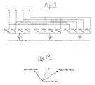
- Figure 10 illustrates the implementation of current source block 226 which, as shown, comprises a plurality of current sources providing currents I W1 ....I w6 each having a pair of transistors associated with it to which inverted and non-inverted versions of the bits of the code value are applied respectively as shown.
- current source block 226 which, as shown, comprises a plurality of current sources providing currents I W1 ....I w6 each having a pair of transistors associated with it to which inverted and non-inverted versions of the bits of the code value are applied respectively as shown.
- the same selection of current values is used to generate both I1+, I1- and I2+, I2-.
- two separate sets of matching current sources are provided, one for each of I1+, I1- and I2+, I2-.
- each of I W1 ??I W6 may have the same magnitude in such an arrangement twelve different phase outputs for the twelve phase steps would be generated as illustrated in Figure 11, which illustrates the equivalent values of W1 and W2 which would be obtained and the corresponding phase diagram. This is also represented in the following table.
- Phase Step PS[1:6] W1 W2 Sum Phase 0 111111 +1.00 0.00 0 1 011111 +0.67 +0.33 27 2 001111 +0.33 +0.67 63 3 000111 0.00 +1.00 90 4 000011 -0.33 +0.67 117 5 000001 -0.67 +0.33 153 6 000000 -1.00 0.00 180 7 100000 -0.67 -0.33 207 8 110000 -0.33 -0.67 243 9 111000 0.00 -1.00 270 10 111100 +0.33 -0.67 297 11 111110 +0.67 -0.33 333
- This sinusoidal current weighting is more advantageous for large values of N, ie. where a fine clock phase resolution is required.
- the performance of the triangular and sinusoidal weighting schemes are virtually equivalent.
- Phase step C1[1:4] C2[1:4] C3[1:4] I1+ I2+ I1- I2- W1 W2 Sum Phase 0 1000 1000 3 0 0 0 +1.00 0.00 0 1 0100 1000 1000 2 1 0 0 +0.67 +0.33 27 2 0100 0100 1000 1 2 0 0 +0.33 +0.67 63 3 0100 0100 0100 0 3 0 0 0.00 +1.00 90 4 0010 0100 0100 0 2 1 0 -0.33 +0.67 117 5 0010 0010 0100 0 1 2 0 -0.67 +0.33 153 6 0010 0010 0010 0 0 3 0 -1.00 0.00 180 7 0001 0010 0010 0 0 2 1 -0.67 -0.33 207 8 0001 0001 0010 0010 0 0 2 1 -0.67 -0.33 207 8 0001 0001 0010 0010 0 0 2
- An arrangement which outputs a pair of reference signals known to have a phase separation of ⁇ /2 from a pair of signals known to have some phase separation, but which phase separation is not known exactly.
- Such an arrangement is advantageous in situations where for example the clock signals are distributed across a chip or circuit board. In such a situation it is possible that some differences in delay may occur between the clocks due to track length or loading, thus altering the phase relationship between the clocks from that which is expected and therefore degrading operation of the circuit.
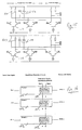
- Fig. 14 is a phasol diagram in which Ref 1 and Ref 2 are received reference clocks. From Ref 1 and Ref 2 are generated sum and difference signals of Ref 1 and Ref 2. It will be appreciated that, if Ref 1 and Ref 2 have the same magnitude then the phase separation between the sum and difference signals is ⁇ /2. Once the magnitudes of the sum and difference signals are equalised therefore, these signals are known to have fixed phase separation and can be used in the embodiments described above.
- Figure 15 illustrates an implementation of this clock phase regeneration arrangement, and it will be seen that this circuit is similar to the phase mixer describer above.
- the upper part of Figure 15 generates the sum signal and comprises two differential circuits 155 to which Ref 1 and Ref 2 are applied as shown and which each have a current source I associated with it.
- the balanced current sources provide equal weightings to Ref 1 and Ref 2 and the sum signals is generated across loading resistors R151 and optional loading capacitors C152.
- the lower part of Figure 15 corresponding generates the difference source, and correspondingly comprises differential circuits 156, current sources I, loading resisitors R153 and optional loading capacitors C154.
- the difference signal is generated by the reversal of the connection of Ref 1 and can be seen from acomparison between the upper and lower and lower parts of Figure 15, Also, an output buffer stage is provided for each of the sum and difference signals after which the signals CLK1 and CLK2 are output for use in the embodiments described above.
- this may be particularly useful in situations where multiple channels of data are being received.
- this pair of clock signals could simply be passed from one channel to the next with phase regeneration being performed as necessary to ensure that quadrature reference signals are available for each channel.
- FIG. 16 Such an arrangement is schematically illustrated in Figure 16 in which clock signals are recovered from received data channels Din.1, Din.2 &Din.n.
- a pair of reference clocks Ref 1, Ref 2 are provided from an external source.
- a clock recovery circuit 160 1 , 160 2 , ...., 160 n is provided and Ref 1 and Ref 2 are applied to circuit 160 1 .
- Each of circuits 160 corresponds to a clock recovery circuit for instance according to one of the embodiments described in detail above and further includes a clock phase regeneration circuit 162.
- Reference clocks Ref 1, Ref2 are applied to channel 1 when circuit 162 1 regenerates their phase relationship and the resulting signals are used to recover clock DRCLK1 and are also passed to channel 2.
- circuit 162 2 regenerates the phase relationship for recovery of clock DRCLK2 and handing on to channel 3.
- This phase regeneration arrangement is also applicable to other circumstances in which quadrature related clock signals are required.
Description
- The present invention relates to devices for synchronising an output signal with an input signal, and in particular to devices which use interpolation or mixing of two reference sources to generate the output.
- Phase locked loops (PLLs) are well known electronic devices and they function to provide an output oscillating signal which is phase locked with an incoming signal. In most PLL architectures, the output signal is generated by a voltage controlled oscillator (VCO) and this output is compared by a phase detector with the input signal. This produces an error signal representing the phase difference between the input and the output and this error is applied, typically via an appropriate filter, to alter the control voltage of the VCO. The oscillating frequency of the VCO is therefore altered until such time as the output is in phase with the input at which time no further error signal is generated and no further changes are made to the control voltage input to the VCO.
- PLLs are typically used where it is desired to generate a clean clock signal synchronised with an incoming signal. One particular application of PLLs is in data transmission systems, for instance communication devices where the transmitted signal is modulated based on a signal having a particular frequency and it is important to recover a corresponding clock signal at the receiver in order to demodulate the received signal.
- In a typical communication system there may be many PLLs in close proximity. For instance there may be PLLs both in the transmit side of the system and in the receive side, and also in a multi-channel system there may be a PLL for each of the channels. If such arrangements are implemented on a single chip problems can occur due to interference between VCOs implemented in such close proximity. Also as data rates increase, the power consumption of the VCO required to generate a satisfactorily low-noise signal increases and this is compounded if more than one VCO is implemented in any particular device.
- It is further known that clock signals may be used in a number of parts of any specific electronic circuitry. In a physical implementation therefore clock signals are carried around a chip or circuit board arrangement by suitable conductive means so as to be transferred from the clock generator to the part of the circuitry dependent on the clock.
- Furthermore, there is shown, from
US Patent 5,526,380 an arrangement for generating a signal of a required phase from quadrature reference signals. - The present invention provides an apparatus for generating an oscillating output signal as set forth in the claims.
- The present invention does not require the presence of a voltage controlled oscillator or other clock source implemented as part of a PLL. Rather it depends on the availability of two or more externally generated reference signals, such as may be available elsewhere in the circuitry as mentioned above.
- In a stand-alone implementation of a PLL according to this invention, there is thus no requirement for a VCO, as the reference signals can be generated from any suitable oscillatory source. This potentially reduces the power requirements of the PLL.
- In an implementation in the context of a communication system as mentioned above, the receiver PLL may be according to this invention and may derive its reference signals from the VCO output in the transmitter side PLL. This removes the possibility of damaging interference between two VCOs on the same chip and also reduces the overall power requirement. Alternatively, both the transmitter and receiver PLLs may receive input clock reference signals from elsewhere.
- This invention is particularly suited to situations such as those referred to above in the communications field where the frequency of the desired output is fairly accurately known as in this case the reference signals would be set to have approximately this frequency. However it is possible and potentially useful within the present invention to generate an output signal having a frequency different from the frequency of the reference signals, and therefore synchronise with an input signal of a different frequency.
- The comparison between the input and the output signal in the invention is broadly the same as the prior art, that is a signal is generated according to phase comparison between the input and the output signals. In the invention this is used to derive and constantly correct the weightings used in the mixing of the reference signals.
- In alternative arrangements, the two references may be arranged non-orthogonal, in which case the relationships between the derived phase relationships and the weighting values is different but can be easily derived. Also it is possible to use three or more references at equal or non-equal phase spacings with appropriate weighting values.
- Quadrature related signals are advantageously used as the reference signals in the PLL, and as will be explained in more detail below a multi-channel communications arrangement can be easily implemented with only one source of clock signals and means arranged to regenerate the quadrature relationship between the clock signals at appropriate points.
- This invention will be better understood from the following description of preferred embodiments which is given by way of example and with reference to the accompanying drawings in which:
- Figure 1 is a schematic drawing of a prior art PLL;
- Figure 2 is a general illustration of the operation of the present invention;
- Figure 3a and 3b illustrate a preferred relationship between the weighting signals and the reference signals in the preferred embodiments of the invention;
- Figure 4 illustrates a first embodiment of the present invention;
- Figure 5 is an example implementation of the phase interpolator of Figure 4;
- Figure 6 is a schematic diagram of an embodiment of the digital filter of Figure 4;
- Figure 7 illustrates a second preferred embodiment of the present invention;
- Figure 8 illustrates the phase interpolator in the embodiment of Figure 7;
- Figure 9 illustrates the phase mixer in the embodiment of Figure 8;
- Figure 10 illustrates the current source block in the embodiment of Figure 8;
- Figure 11 illustrates a first coding scheme representing the phase steps in the embodiment of Figure 7;
- Figure 12 illustrates a second coding scheme representing the phase steps in the embodiment of Figure 7;
- Figure 13 illustrates the operation of an alternative current weighting control arrangement;
- Figure 14 illustrates a known principle of operation;
- Figure 15 illustrates an implementation of the principles illustrated in Figure 14; and
- Figure 16 illustrates a further exemplary embodiment of the invention.
- In broad terms, the invention is apparatus for producing an oscillating signal in a predetermined phase relationship with an input signal which generates its output signal by mixing in variable proportions two or more reference oscillating signals. Preferably the reference signals should be in quadrature relationship and have approximately the same frequency as the desired output, but this is not essential. The output signal may be desired to be in phase with the input signal or to have a predetermined phase offset. In a further aspect, apparatus is described which generates quadrature related clock signals, which may be used as the reference signals in the phase-lock arrangement.
- Figure 1 illustrates in schematic form a schematic diagram of a prior art PLL the operation of which is useful to understand for the understanding of the present invention. The PLL illustration in Figure 1 comprises a voltage controlled oscillator (VCO) 10 which has a control voltage applied to it and which outputs a
clock signal 12. As is well known the frequency of theoutput 12 is a function of the magnitude of the control voltage enabling the frequency ofoutput 12 to be controlled by varying the control voltage. The PLL has input to it asignal 14, for instance a data signal based on a remotely derived clock signal, and it is desired thatclock signal 12 should be synchronised withinput signal 14. These two signals are compared byphase detector 16 which compares the phases of the two signals in order to generate asignal 18 according to the phase difference betweensignals signal 18 indicates whether the frequency ofoutput signal 12 needs to increase or decrease in order to bringsignals VCO 10 such that the control voltage increases and decreases according tosignal 18. - A PLL is therefore essentially a closed loop control system which compares the input and the output and controls the generation of the output according to the result of that comparison.
- Figure 2 illustrates in general terms the operation of the preferred embodiments of the present invention. The same reference numerals as were used in Figure 1 are used in Figure 2 for corresponding components.
- The device in Figure 2 has input thereto
signal 14 and it is arranged to generateoutput signal 12 which is intended to have a particular phase relationship with theinput signal 14. In the following description it will be assumed thatsignal 12 is intended to be in phase withinput signal 14, but it will be apparent that simple alterations can be made to the parameters of operation to achieve any desired phase relationship. In the same way as in Figure 1signals phase detector 16 which providesoutput 18 indicating whether the frequency ofsignal 12 needs to be increased or decreased to bring it more in phase withsignal 14. - In Figure 2 however
signal 12 is not generated as the output of a voltage control oscillator. Rather, it is the output of the mixing means 20. Mixing means 20 has input to it two reference signals or clock sources CLK1 and CLK2. Signals CLK1 and CLK2 have the same frequencies as each other but are out of phase, and in the particularly preferred embodiment these two signals are 90° out of phase as illustrated in the phasor diagram in Figure 3a. Mixing means 20 mixes signals CLK1 and CLK2 in variable proportions in accordance withoutput 18 fromphase detector 16 in order to generateoutput 12. The proportions in which the signals CLK1 and CLK2 are mixed together vary sinusoidally between -1 and +1 as described in more detail below in order thatoutput signal 12 may have any phase relationship with the reference clock signals. - In particular in Figure 3a the generation of an output signal 150° out of phase with reference CLK1 is illustrated by way of example and it is shown that in order to generate this signal it is necessary to mix reference signals CLK1 and CLK2 in the proportions -0.866 to 0.5. In general, in order to generate a signal having a phase difference P as compared to
CLK 1 it is necessary to mix reference signals CLK1 and CLK2 in the proportions cos P to sin P. - This is illustrated in Figure 3b where the weighting given to reference signal CLK1 is designated W1 and that given to signal CLK2 is designated W2. Figure 3b illustrates the values taken by W1 and W2 in order to generate various phase differences P as compared to reference signal CLK1, with 150° again shown as an example.
- One implementation of this embodiment is in the context of communication systems, and in particular in the receive side. In such a context, the reference signals CLK1 and CLK2 may be derived from signals generated in the transmit side VCO, but the reference signals may be derived from any suitable source.
- Figure 4 illustrates one embodiment in which the above sin and cos values are determined using look-up tables. In this embodiment, mixing means 20 comprises digital filter 122 which generates value P according to signal 18 output by
phase detector 16. In this figure the reference clock signals are designated φ1 and φ2 and are illustrated, by way of example as being received from a VCO forming part of another PLL. Any other suitable source of clock signals could however be utilised. Value P represents the desired phase difference between reference signal φ1 andoutput signal 12 in order to keepsignal 12 in synchronisation withinput signal 14. Once synchronisation has been achieved, signal 18 will not indicate that any increase or decrease in frequency is required to bring the signals into phase, and therefore in such a state digital filter 122 outputs a constant value of P to maintain the established phase relationships. (A slightly different situation occurs if the input signal has a different frequency to the reference signals as discussed below). - As mentioned above, in general terms the desired value of W1 is cos P and the desired value of W2 is sin P. In this embodiment there are therefore provided two look up tables 124a and 124b to which P is applied and which output, in digital form, the cosine and sine of P respectively. These signals are passed through digital to analogue converters 126a and 126b respectively in order to provide analogue signals W1 and W2 for input to phase
interpolator 120.Phase interpolator 120 mixes φ1 and φ2 in the proportions determined by W1 and W2 to generateoutput signal 12. - Thus it is the case that
output signal 12 can be locked to be in phase withinput signal 14 whatever the phase relationship betweeninput signal 14 and the reference signals φ1 and φ2. - Figure 5 illustrates one possible implementation of
phase interpolator 120 based on differential MOS circuit techniques in which each signal in Figure 4 is illustrated by two signals in Figure 5 having corresponding names with a and b suffixes. The implementation illustrated in Figure 5 enables W1 and W2 to vary over the complete range -1 to +1 enablingphase interpolator 120 to fully implement the functions discussed above. - Digital filter 122 illustrated in Figure 4 may simply be an up/down counter. This would count up or down according to the polarity of
input signal 18 until the desired value of P is being output at whichtime signal 18 would go to 0 and the value of P would remain constant at its desired locked value. The counter should be arranged to wrap around, when incrementing above the maximum count or decrementing below 0 in order to provide a fully functional device. - The above discussion has been based on the assumption that the reference signals are operating at the same frequency as the input signal and therefore have the same frequency as the desired frequency of
signal 12. - The circuit illustrated in Figure 4 will however also operate in the situation where the frequency of
signal 14 and therefore the desired frequency ofsignal 12 is different from the frequency of the reference signals φ1 and φ2. Such a situation is equivalent to a situation where the phase difference betweensignal 14 and reference signal φ1 is constantly changing and therefore the value of P must also be constantly changing. This would be achieved in Figure 4 with no further alternations to the circuit because the "steady state" condition of the circuit would be wheresignal 18 was constantly indicating a phase difference causing the value of P to change in synchronism with the constantly changing phase difference betweensignal 14 and reference signal φ1. - This function could be achieved using the simple counter for digital filter 122 mentioned above and this would work satisfactorily for input signals 14 which are constantly providing signal transitions by way of which the phase can be compared by
phase detector 16. - However, in a situation where the input data has a low transition density, that is the input signal may effectively be inactive for lengthy periods of time, the loop will have difficulty tracking the required phase and would have to make significant changes in the phase of
output signal 12 each time a burst of activity occurred. Figure 6 illustrates an alternative implementation of digital filter 122 which overcomes this problem. - Digital filter 122 as illustrated in Figure 6 comprises a
counter 50, amultiplier 52 and anaccumulator 54. Thesignal 18 indicating whether the phase ofoutput signal 12 needs to be increased or decreased in order to achieve synchronism is input both to counter 50 and toaccumulator 54.Counter 50 counts up or down according to the value ofsignal 18 to produce signal F which is multiplied by a constant K inmultiplier 52 and is also input toaccumulator 54.Accumulator 54 generates a new output value of P by adding, to the existing value of P, the two inputs it receives. -
Counter 50 in this implementation effectively integrates the increment/ decrement pulses ofsignal 18 so as to produce the value F. Value F therefore represents the frequency offset between the frequency of the reference signals and desired frequency forsignal 12. As mentioned above, this frequency difference is equivalent to a constantly changing phase difference and therefore this can be accounted for by constantly changing the value of P to track this phase difference. The effect of constant K ofmultiplier 52 and the addition of the multiplied signal intoaccumulator 54 is to cause signal P to track at the necessary rate of change of phase so as to synchronise with the different frequency signal. - When the loop is locked to the incoming signal, signal 18 will be effectively 0 as there will be no phase difference between the input and the output. In this condition, the steady state is for the value of F X K to be added on each cycle to value P by
accumulator 54 to cause the necessary ongoing phase changes to keep the system in synchronism. This will continue even when there is inactivity in the input signal so that, ideally, the system is still synchronised at the time of the next burst. In any event, the level of phase correction required at the beginning of the next burst will be reduced. - The
signal 18 is also input directly toaccumulator 54 so that when the system is not in the locked condition it will lock in properly and provide a stable system. - Figure 7 illustrates a particularly preferred implementation of the invention, the details of which are illustrated in the succeeding figures. It will be seen that the principles behind the implementation are similar to those outlined above, but the actual circuits used are different and, in certain circumstances, more practical.
- In the embodiment of Fig. 7, mixing means 20 comprises a digital control means 210 and
phase interpolator 220, and the embodiment is described in terms of clock memory based on a serial data input. - As with the embodiment described above, a standard
phase detector circuit 16 is used to compare the positions of the edges in theserial data input 14 with the phase of thedata recovery clock 12. This produces phase increment/decrement control signals which are fed intodigital logic block 210 which generates a control word representing the required phase of the data recovery clock. The digital phase select value is then applied to thephase interpolator 220 which uses an analogue mixer to derive the required data recovery clock phase from the two reference clock phases. - An optional reference regeneration circuit may be included to restore the quadrature phase relationship between the reference clock phases, thus allowing the effects of skew due to distribution of the clocks to be reduced. Details of this regeneration circuit are set out below.
- Broadly, as illustrated in Figure 8 the
phase interpolator 220 in this embodiment is formed of an analogue phase mixer 222 and a digitally controlledcurrent source block 226. The current source block 226 provides current signals to the phase mixer 222 to provide, as discussed in more detail below, the weightings in which the reference signals CLK1 and CLK2 should be mixed. - A schematic illustration of an implementation of the phase mixer 222 based on differential techniques, in which each signal is represented by a pair of signal lines, is shown in Figure 9. The required weightings for the reference signals are provided by the current source block 226 as currents I1+, I1-, I2+, I2- which appear as current sources in Figure 9. The circuit of Figure 9 sums the reference clock signals according to the weights of their control currents to generate a Sum signal represented by the differential voltage developed across load resistors R1 and R2.
- The load capacitances (C1 and C2) are optional and may be included to filter out harmonics of the clock signals to reduce distortion of the Sum signal. The described operation assumes the use of sinusoidal reference clock signals. However, square clocks may also be used but require filtering either by C1 and C2, and/or by the intrinsic bandwidth limit of the phase summing circuit.
- Phase mixer 222 comprises four differential amplifiers 91a, 91b, 92a, 92b each of which includes two transistors as illustrated in a conventional fashion. Reference clock CLK1 is applied as shown to amplifiers 91a and 91b with opposite polarities. The provision of two amplifiers connected with opposite polarities means that one acts to add the reference clock to the Sum signal, while the other subtracts it. The current sources I1+, I1- control the relative extents to which the amplifiers add and subtract the reference signal, and thus the current pair I1+ and I1- constitute a differential current weighting representing W1 in Figure 3 above enabling W1 to be adjusted from +1 to -1.
- The values of I1+ and I1- are set by current source block 226 which keeps the total Itot = (I1+) + (I1-) constant. The value of W1 is therefore represented by appropriate selection of I1+ and I1-. In particular,


- Current source pair I2+, I2- are similarly varied between 0 and Itot in order to represent the value of W2 between +1 and -1 and these are associated with amplifiers 92a, 92b to which the reference clock CLK2 is applied with opposite polarities.
- In summary then, by varying the weight currents I1+, I1-, I2+, I2- the weightings W1, W2 for the reference clocks CLK1, CLK2 can be varied as discussed above in relation to Figure 3 such that the phase of the Sum signal can be varied over a whole cycle.
- Finally, the Sum signal is buffered using a second
differential amplifier stage 94 to "square up" the signal and remove any amplitude variation resulting from the phase mixing operation to generate thesecond clock signal 12. - The differential weighting currents I1+, I1-, I2+, I2- are generated by
block 226 by digitally controlling a set of switched current sources, which will be described in detail later. From the above discussion it will be understood that any one desired phase difference from, say, reference CLK1 defines a pair of values W1, W2 and accordingly a set of I1+, I1-, I2+, I2-. The particular phase required is indicated to block 226 by the digital control word output by digital control means 210 as the phase select signal. - In this embodiment, in order to simplify the generation of the current weightings the digital control value is encoded using a Johnson (twisted-ring) counter type code. This uses an N-bit word, PS[1:N], (where N is an even integer) to define 2N possible code values which are used to designate 2N available phase steps which may be output by the interpolator.
- The value of N therefore effectively determines the phase resolution of the clock alignment circuitry: since there are 2N phase steps over one complete cycle (2π radians), the phase resolution is π/N radians. The value of N is therefore chosen to trade off phase resolution with complexity. The described embodiment assumes a value of N=6, thus providing a phase alignment resolution of 1/12th of a cycle (ie. 30°). The 12 possible code values for a 6-bit implementation of the phase select are as follows:
Step PS[1:6] Step PS[1:6] 0 111111 6 000000 1 011111 7 100000 2 001111 8 110000 3 000111 9 111000 4 000011 10 111100 5 000001 11 111110 - Figure 10 illustrates the implementation of current source block 226 which, as shown, comprises a plurality of current sources providing currents IW1....Iw6each having a pair of transistors associated with it to which inverted and non-inverted versions of the bits of the code value are applied respectively as shown. As shown in Figure 10, the same selection of current values is used to generate both I1+, I1- and I2+, I2-. As shown, two separate sets of matching current sources are provided, one for each of I1+, I1- and I2+, I2-. However, it may be possible to use one set of current sources together with appropriate timing and switching circuitry to generate alternately I1+, I1- and I2+, I2-.
- An advantage of using this coding scheme is that the weighting controls for the two different phases can be derived from the same set of control lines: for W2 the control word needs to be rotated by N/2 bits, inverting the bits that are wrapped around. This can effectively be achieved simply by swapping over the control lines of the differential current switches as illustrated in Figure 10.
- In a simple arrangement, each of IW1.....IW6 may have the same magnitude in such an arrangement twelve different phase outputs for the twelve phase steps would be generated as illustrated in Figure 11, which illustrates the equivalent values of W1 and W2 which would be obtained and the corresponding phase diagram. This is also represented in the following table.
Phase Step PS[1:6] W1 W2 Sum Phase 0 111111 +1.00 0.00 0 1 011111 +0.67 +0.33 27 2 001111 +0.33 +0.67 63 3 000111 0.00 +1.00 90 4 000011 -0.33 +0.67 117 5 000001 -0.67 +0.33 153 6 000000 -1.00 0.00 180 7 100000 -0.67 -0.33 207 8 110000 -0.33 -0.67 243 9 111000 0.00 -1.00 270 10 111100 +0.33 -0.67 297 11 111110 +0.67 -0.33 333 - It will be seen that this provides variations in the phase step size around the cycle. This may not present problems in some circumstances, but a constant step size providing optimum phase resolution can be obtained by setting the current weightings according to the following:

- IW1 = 0.067 Itot
- IW2 = 0.183 Itot
- Iw3 = 0.250 Itot
- IW4 = 0.250 Itot
- IW5 = 0.183 Itot
- IW6 = 0.067 Itot
- This arrangement provides sinusoidal variations in the equivalent values of W1 and W2 and even phase step size as illustrated in Figure 12, which corresponds to Figure 11 in format, and as represented in the following table.
Phase Step PS[1:6] W1 W2 Sum Phase 0 111111 + 1.00 0.00 0 1 011111 +0.87 +0.50 30 2 001111 +0.50 +0.87 60 3 000111 0.00 +1.00 90 4 000011 -0.50 +0.87 120 5 000001 -0.87 +0.50 150 6 000000 -1.00 0.00 180 7 100000 -0.87 -0.50 210 8 110000 -0.50 -0.87 240 9 111000 0.00 -1.00 270 10 111100 +0.50 -0.87 300 11 111110 +0.87 -0.50 330 - This sinusoidal current weighting is more advantageous for large values of N, ie. where a fine clock phase resolution is required. However, for example, if N=4 (ie. 1/8 cycle resolution) the performance of the triangular and sinusoidal weighting schemes are virtually equivalent.
- If performance offered by the triangular current weighting schemes is sufficient, the current control can be implemented using an alternative arrangement illustrated in Figure 13 and represented by the following table.
Phase step C1[1:4] C2[1:4] C3[1:4] I1+ I2+ I1- I2- W1 W2 Sum Phase 0 1000 1000 1000 3 0 0 0 +1.00 0.00 0 1 0100 1000 1000 2 1 0 0 +0.67 +0.33 27 2 0100 0100 1000 1 2 0 0 +0.33 +0.67 63 3 0100 0100 0100 0 3 0 0 0.00 +1.00 90 4 0010 0100 0100 0 2 1 0 -0.33 +0.67 117 5 0010 0010 0100 0 1 2 0 -0.67 +0.33 153 6 0010 0010 0010 0 0 3 0 -1.00 0.00 180 7 0001 0010 0010 0 0 2 1 -0.67 -0.33 207 8 0001 0001 0010 0 0 1 2 -0.33 -0.67 243 9 1000 0001 0001 0 0 0 3 0.00 -1.00 270 10 1000 0001 0001 1 0 0 2 +0.33 -0.67 297 11 1000 1000 0001 2 0 0 1 +0.67 -0.33 333 - This is based on the use of a set of 4:1 current switches to switch equally-weighted current sources I1, I2, I3 onto one of the 4 differential amplifier control currents. This scheme uses only half the number of current sources as the previous arrangement, and a different coding scheme, The number of current sources/switches again determines the resolution of the clock steps. For example, if M current sources are used, each with a 4:1 current switch, this provides 4M phase steps across one cycle (but also requires 4M control lines). The example shown in Figure 8 uses 3 current sources to provide a 1/12 cycle resolution.
- In the description of the embodiments above, it is assumed that the two reference clocks are in quadrature, ie, separated in phase by π/2 radians (90°). While it is possible to design the overall circuit to use reference clocks having a different phase separation, this increases the complexity of the calculation and the circuitry required to set the weighting values for the mixing means. In any event it will always be important to know the phase separation between the reference clocks when determining the weighting values to ensure proper functioning of the circuit.
- An arrangement is known which outputs a pair of reference signals known to have a phase separation of π/2 from a pair of signals known to have some phase separation, but which phase separation is not known exactly. Such an arrangement is advantageous in situations where for example the clock signals are distributed across a chip or circuit board. In such a situation it is possible that some differences in delay may occur between the clocks due to track length or loading, thus altering the phase relationship between the clocks from that which is expected and therefore degrading operation of the circuit.
- The principle of operation is illustrated in Fig. 14 which is a phasol diagram in which
Ref 1 andRef 2 are received reference clocks. FromRef 1 andRef 2 are generated sum and difference signals ofRef 1 andRef 2. It will be appreciated that, ifRef 1 andRef 2 have the same magnitude then the phase separation between the sum and difference signals is π/2. Once the magnitudes of the sum and difference signals are equalised therefore, these signals are known to have fixed phase separation and can be used in the embodiments described above. Figure 15 illustrates an implementation of this clock phase regeneration arrangement, and it will be seen that this circuit is similar to the phase mixer describer above. The upper part of Figure 15 generates the sum signal and comprises twodifferential circuits 155 to whichRef 1 andRef 2 are applied as shown and which each have a current source I associated with it. The balanced current sources provide equal weightings toRef 1 andRef 2 and the sum signals is generated across loading resistors R151 and optional loading capacitors C152. The lower part of Figure 15 corresponding generates the difference source, and correspondingly comprisesdifferential circuits 156, current sources I, loading resisitors R153 and optional loading capacitors C154. The difference signal is generated by the reversal of the connection ofRef 1 and can be seen from acomparison between the upper and lower and lower parts of Figure 15, Also, an output buffer stage is provided for each of the sum and difference signals after which the signals CLK1 and CLK2 are output for use in the embodiments described above. - In principle, this technique could be used to distribute a pair of clocks over an unlimited distance with no accumulated error in their phase difference. Clock regeneration circuits as described above would be provided along the clock path functioning as repeaters.
- In the context of the clock recovery from data signals as described in the embodiments above, this may be particularly useful in situations where multiple channels of data are being received. In such an arrangement, this pair of clock signals could simply be passed from one channel to the next with phase regeneration being performed as necessary to ensure that quadrature reference signals are available for each channel.
- Such an arrangement is schematically illustrated in Figure 16 in which clock signals are recovered from received data channels Din.1, Din.2 .....Din.n. For this purpose, a pair of
reference clocks Ref 1,Ref 2 are provided from an external source. For each channel aclock recovery circuit Ref 1 andRef 2 are applied tocircuit 1601. Each ofcircuits 160 corresponds to a clock recovery circuit for instance according to one of the embodiments described in detail above and further includes a clock phase regeneration circuit 162. -
Reference clocks Ref 1, Ref2 are applied tochannel 1 when circuit 1621 regenerates their phase relationship and the resulting signals are used to recover clock DRCLK1 and are also passed tochannel 2. Correspondingly circuit 1622 regenerates the phase relationship for recovery of clock DRCLK2 and handing on tochannel 3. Depending on the physical layout of the circuitry it may not be necessary to regenerate the phase at every step, but providing regeneration as necessary results in a simpler overall arrangement than local generation of clock references for each channel - This phase regeneration arrangement is also applicable to other circumstances in which quadrature related clock signals are required.
Claims (9)
- Apparatus for generating an oscillating output signal (12) having a desired phase relationship with an input signal (14), comprising:mixing means (20) arranged to received first and second reference signals (Clk1,Clk2) oscillating at a common frequency and having a phase offset between them, and to mix said first and second reference signals in variable proportions to generate said output signal; andcomparing means (16) arranged to compare the phase of said output signal (12) with said input signal (14) and to provide a comparison output signal (18) indicative of whether the phase of said generated output signal is in said desired phase relationship with said input signal;said mixing means (20) being responsive to said comparison output signal (18) to alter said proportions in which said first and second reference signals are mixed; characterised in that the mixing proportion for each of said reference signals is represented by a pair of differential weighting current signals and said mixing means (20) comprises a plurality of differential amplifiers with each reference signal being applied to two of said differential amplifiers with opposite polarity and current in said two differential amplifiers being supplied respectively by a corresponding pair of differential weighting current signals, the sum of the outputs of said differential amplifiers being used to provide said output signal (12).
- Apparatus according to claim 1 in which said first and second reference signals are in quadrature relationship with each other.
- Apparatus according to claim 2 in which said mixing means (20) comprises arranged to mix said first and second reference signals in proportions which vary sinusoidally with the required phase difference between the output and one of said first and second reference signals.
- Apparatus according to any of claims 1 to 3 in which said mixing means (20) comprises means arranged to output a signal indicative of the desired phase relationship between said output signal and one of said reference signals
- Apparatus according to claims 3 in which said mixing means (20) comprising means arranged to output a multi-bit signal indicative of the desired phase relationship between said output signal and one of said reference signals, and current mixing means comprising a plurality of current sources, the outputs of which are selectively added together according to the values of bits in said multi-bit signal to output said differential weight current signals.
- Apparatus according to claim 5 in which said plurality of current sources are all of the same current value.
- Apparatus according to claim 5 in which the current values of said current sources differ from each other to facilitate the generation of differential weighting current signals representing mixing proportions for said reference signals which result in evenly phase spaced output signals.
- Apparatus according to any of any preceding claim which said mixing means (20) comprises means (122) arranged to output a signal indicative of the defined phase relationship between said output signal and one of said reference signals, and look-up table means (124a,124b) to derive from said signal said mixing proportions.
- Apparatus according to claim 8 in which said look-up table means (124a,124b) comprise sine and cosine tables.
Applications Claiming Priority (2)
| Application Number | Priority Date | Filing Date | Title |
|---|---|---|---|
| GB9721384 | 1997-10-08 | ||
| GBGB9721384.7A GB9721384D0 (en) | 1997-10-08 | 1997-10-08 | Phase locked loop |
Publications (3)
| Publication Number | Publication Date |
|---|---|
| EP0909035A2 EP0909035A2 (en) | 1999-04-14 |
| EP0909035A3 EP0909035A3 (en) | 2000-09-06 |
| EP0909035B1 true EP0909035B1 (en) | 2007-10-17 |
Family
ID=10820263
Family Applications (1)
| Application Number | Title | Priority Date | Filing Date |
|---|---|---|---|
| EP98308210A Expired - Lifetime EP0909035B1 (en) | 1997-10-08 | 1998-10-08 | Phase synchronisation device and phase quadrature signal generating apparatus |
Country Status (4)
| Country | Link |
|---|---|
| US (2) | US6107848A (en) |
| EP (1) | EP0909035B1 (en) |
| DE (1) | DE69838574T2 (en) |
| GB (1) | GB9721384D0 (en) |
Cited By (3)
| Publication number | Priority date | Publication date | Assignee | Title |
|---|---|---|---|---|
| US8223828B2 (en) | 2000-04-28 | 2012-07-17 | Broadcom Corporation | Methods and systems for adaptive receiver equalization |
| US8299834B2 (en) | 1999-06-28 | 2012-10-30 | Broadcom Corporation | Current-controlled CMOS logic family |
| US8750320B2 (en) | 1997-01-23 | 2014-06-10 | Broadcom Corporation | Fibre channel arbitrated loop bufferless switch circuitry to increase bandwidth without significant increase in cost |
Families Citing this family (31)
| Publication number | Priority date | Publication date | Assignee | Title |
|---|---|---|---|---|
| TW483255B (en) * | 1999-11-26 | 2002-04-11 | Fujitsu Ltd | Phase-combining circuit and timing signal generator circuit for carrying out a high-speed signal transmission |
| GB2362045B (en) * | 2000-02-23 | 2004-05-05 | Phoenix Vlsi Consultants Ltd | Analogue-Controlled phase interpolator |
| US6329859B1 (en) * | 2000-03-23 | 2001-12-11 | Bitblitz Communications, Inc. | N-way circular phase interpolator for generating a signal having arbitrary phase |
| US7564866B2 (en) | 2000-07-21 | 2009-07-21 | Broadcom Corporation | Methods and systems for digitally processing optical data signals |
| US7245638B2 (en) | 2000-07-21 | 2007-07-17 | Broadcom Corporation | Methods and systems for DSP-based receivers |
| US6969984B2 (en) * | 2000-12-21 | 2005-11-29 | Tropian, Inc. | Direct phase and frequency demodulation |
| US6931089B2 (en) * | 2001-08-21 | 2005-08-16 | Intersil Corporation | Phase-locked loop with analog phase rotator |
| US6922109B2 (en) | 2002-04-01 | 2005-07-26 | Broadcom Corporation | Multiple synthesized clocks with fractional PPM control from a single clock source |
| US7162002B2 (en) * | 2002-03-01 | 2007-01-09 | Broadcom Corporation | Phase-interpolator based PLL frequency synthesizer |
| US7379520B2 (en) * | 2002-04-01 | 2008-05-27 | Broadcom Corporation | Low jitter phase rotator |
| US7266169B2 (en) * | 2002-09-13 | 2007-09-04 | Broadcom Corporation | Phase interpolater and applications thereof |
| EP1469629A1 (en) * | 2003-04-14 | 2004-10-20 | Infineon Technologies AG | Method and apparatus for generating a phase shifted output clock signal |
| KR100539978B1 (en) * | 2003-04-28 | 2006-01-10 | 삼성전자주식회사 | Circuits and method for mixing frequency, and circuits and method for receiving radio frequency |
| US6940352B2 (en) * | 2003-11-26 | 2005-09-06 | Scintera Networks, Inc. | Analog signal interpolation |
| US7187917B2 (en) * | 2004-03-29 | 2007-03-06 | Texas Instruments Incorporated | Current interpolation in multi-phase local oscillator for use with harmonic rejection mixer |
| US7457346B2 (en) * | 2004-04-05 | 2008-11-25 | Alan Fiedler | Spread-spectrum signal generator |
| GB0413149D0 (en) * | 2004-06-12 | 2004-07-14 | Texas Instruments Ltd | Improvements in or relating to interpolation |
| US7298194B2 (en) * | 2004-06-12 | 2007-11-20 | Texas Instruments Incorporated | Interpolation |
| GB0413071D0 (en) * | 2004-06-12 | 2004-07-14 | Texas Instruments Ltd | Triangulating phase interpolator |
| DE102004037160B3 (en) | 2004-07-30 | 2006-03-16 | Infineon Technologies Ag | A method and apparatus for generating an output clock signal having an adjustable phase position from a plurality of input clock signals |
| US7161443B2 (en) | 2004-09-30 | 2007-01-09 | Broadcom Corporation | Temperature compensated crystal oscillator |
| US8228110B1 (en) | 2004-12-06 | 2012-07-24 | Marvell International Ltd. | Low power, low voltage phase interpolator |
| US7400184B2 (en) * | 2005-04-22 | 2008-07-15 | Sitel Semiconductor B.V. | Current mode multiplier based on square root voltage-current relationship of MOS transistor |
| US7403048B2 (en) * | 2005-06-01 | 2008-07-22 | Wilinx Corporation | Divider circuits and methods using in-phase and quadrature signals |
| US7196564B2 (en) * | 2005-07-22 | 2007-03-27 | Texas Instruments Incorporated | High frequency balanced phase interpolator |
| DE102006023695B4 (en) * | 2006-05-19 | 2010-04-08 | Xignal Technologies Ag | Method and circuit arrangement for generating a periodic electrical signal with controllable phase |
| US7498889B2 (en) * | 2006-08-03 | 2009-03-03 | Intel Corporation | Analog phase controller |
| US7924885B2 (en) * | 2006-11-20 | 2011-04-12 | Siverge Networks Ltd | Methods and apparatuses for circuit emulation multi-channel clock recovery |
| US8643414B1 (en) * | 2012-02-13 | 2014-02-04 | Rambus Inc. | Fast locking phase-locked loop |
| US8896358B2 (en) * | 2012-11-08 | 2014-11-25 | Avago Technologies General Ip (Singapore) Pte. Ltd. | Phase interpolator having adaptively biased phase mixer |
| US9160345B1 (en) * | 2014-09-04 | 2015-10-13 | Inphi Corporation | Phase interpolator |
Family Cites Families (5)
| Publication number | Priority date | Publication date | Assignee | Title |
|---|---|---|---|---|
| AU570439B2 (en) * | 1983-03-28 | 1988-03-17 | Compression Labs, Inc. | A combined intraframe and interframe transform coding system |
| GB2239141B (en) * | 1989-12-15 | 1993-05-12 | Stc Plc | Phase splitter arrangement |
| US5526380A (en) * | 1994-06-07 | 1996-06-11 | Texas Instruments Incorporated | First-order loop control configuration for a phase-rotator based clock synchronization circuit |
| EP0707379A1 (en) * | 1994-10-11 | 1996-04-17 | BELL TELEPHONE MANUFACTURING COMPANY Naamloze Vennootschap | Tunable quadrature phase shifter |
| GB2329775A (en) * | 1997-09-26 | 1999-03-31 | Nec Corp | Operational transconductance amplifier, squarer and hyperbolic sine/cosine circuits using a bypass transistor in a differential stage |
-
1997
- 1997-10-08 GB GBGB9721384.7A patent/GB9721384D0/en not_active Ceased
-
1998
- 1998-10-08 EP EP98308210A patent/EP0909035B1/en not_active Expired - Lifetime
- 1998-10-08 DE DE69838574T patent/DE69838574T2/en not_active Expired - Lifetime
- 1998-10-08 US US09/167,989 patent/US6107848A/en not_active Expired - Lifetime
-
2000
- 2000-07-07 US US09/612,380 patent/US6242965B1/en not_active Expired - Lifetime
Cited By (10)
| Publication number | Priority date | Publication date | Assignee | Title |
|---|---|---|---|---|
| US8750320B2 (en) | 1997-01-23 | 2014-06-10 | Broadcom Corporation | Fibre channel arbitrated loop bufferless switch circuitry to increase bandwidth without significant increase in cost |
| US8299834B2 (en) | 1999-06-28 | 2012-10-30 | Broadcom Corporation | Current-controlled CMOS logic family |
| US8823435B2 (en) | 1999-06-28 | 2014-09-02 | Broadcom Corporation | Current-controlled CMOS logic family |
| US9112487B2 (en) | 1999-06-28 | 2015-08-18 | Broadcom Corporation | Current-controlled CMOS logic family |
| US9831853B2 (en) | 1999-06-28 | 2017-11-28 | Avago Technologies General Ip (Singapore) Pte. Ltd. | Current-controlled CMOS logic family |
| US8223828B2 (en) | 2000-04-28 | 2012-07-17 | Broadcom Corporation | Methods and systems for adaptive receiver equalization |
| US8433020B2 (en) | 2000-04-28 | 2013-04-30 | Broadcom Corporation | High-speed serial data transceiver and related methods |
| US8472512B2 (en) | 2000-04-28 | 2013-06-25 | Broadcom Corporation | Methods and systems for adaptive receiver equalization |
| US8798219B2 (en) | 2000-04-28 | 2014-08-05 | Broadcom Corporation | High-speed serial data transceiver and related methods |
| US8824538B2 (en) | 2000-04-28 | 2014-09-02 | Broadcom Corporation | Methods and systems for adaptive receiver equalization |
Also Published As
| Publication number | Publication date |
|---|---|
| GB9721384D0 (en) | 1997-12-10 |
| US6107848A (en) | 2000-08-22 |
| DE69838574T2 (en) | 2008-07-24 |
| DE69838574D1 (en) | 2007-11-29 |
| EP0909035A2 (en) | 1999-04-14 |
| EP0909035A3 (en) | 2000-09-06 |
| US6242965B1 (en) | 2001-06-05 |
Similar Documents
| Publication | Publication Date | Title |
|---|---|---|
| EP0909035B1 (en) | Phase synchronisation device and phase quadrature signal generating apparatus | |
| US10686584B2 (en) | Quadrature and duty cycle error correction in matrix phase lock loop | |
| US7724862B2 (en) | Phase locked loop apparatus with adjustable phase shift | |
| US5315269A (en) | Phase-locked loop | |
| EP1341309B1 (en) | Phase-interpolator based PLL frequency synthesizer | |
| US7636007B2 (en) | Low jitter high phase resolution PLL-based timing recovery system | |
| EP1609243B1 (en) | Method and system of jitter compensation | |
| US5270669A (en) | Local oscillating frequency synthesizer for use in a TDMA system | |
| EP1721388B1 (en) | Fractional frequency synthesizer | |
| CA2201695C (en) | Phase detector for high speed clock recovery from random binary signals | |
| EP0652642A1 (en) | Method and apparatus for a phase-locked loop circuit with holdover mode | |
| AU3330399A (en) | Phase detector | |
| US20210273644A1 (en) | Apparatus and methods for digital fractional phase locked loop with a current mode low pass filter | |
| KR20000035274A (en) | Phase detector with frequency steering | |
| US20020057118A1 (en) | Apparatus and method for counting high-speed early/late pulses from a high speed phase detector using a pulse accumulator | |
| Yang | Delay-locked loops-an overview | |
| US20030062959A1 (en) | Fractional N frequency synthesizer | |
| JPH04260219A (en) | Phase synchronizing loop synthesizer | |
| KR20070065414A (en) | Sigma-delta based phase lock loop | |
| JP2929965B2 (en) | Wireless communication terminal | |
| Floyd | Sub-integer frequency synthesis using phase-rotating frequency dividers | |
| EP1145440B1 (en) | Low jitter high phase resolution pll-based timing recovery system | |
| US5903593A (en) | Spread spectrum signal receiver | |
| US6265919B1 (en) | In phase alignment for PLL's | |
| JPH1032489A (en) | Digital delay controlled clock generator and delay locked loop using the clock generator |
Legal Events
| Date | Code | Title | Description |
|---|---|---|---|
| PUAI | Public reference made under article 153(3) epc to a published international application that has entered the european phase |
Free format text: ORIGINAL CODE: 0009012 |
|
| AK | Designated contracting states |
Kind code of ref document: A2 Designated state(s): DE FI FR GB IT NL SE |
|
| AX | Request for extension of the european patent |
Free format text: AL;LT;LV;MK;RO;SI |
|
| PUAL | Search report despatched |
Free format text: ORIGINAL CODE: 0009013 |
|
| AK | Designated contracting states |
Kind code of ref document: A3 Designated state(s): AT BE CH CY DE DK ES FI FR GB GR IE IT LI LU MC NL PT SE |
|
| AX | Request for extension of the european patent |
Free format text: AL;LT;LV;MK;RO;SI |
|
| RIC1 | Information provided on ipc code assigned before grant |
Free format text: 7H 03L 7/08 A, 7H 03L 7/081 B, 7H 03H 11/22 B |
|
| 17P | Request for examination filed |
Effective date: 20010122 |
|
| AKX | Designation fees paid |
Free format text: DE FI FR GB IT NL SE |
|
| 17Q | First examination report despatched |
Effective date: 20031017 |
|
| RAP1 | Party data changed (applicant data changed or rights of an application transferred) |
Owner name: TEXAS INSTRUMENTS LIMITED |
|
| GRAP | Despatch of communication of intention to grant a patent |
Free format text: ORIGINAL CODE: EPIDOSNIGR1 |
|
| GRAS | Grant fee paid |
Free format text: ORIGINAL CODE: EPIDOSNIGR3 |
|
| GRAA | (expected) grant |
Free format text: ORIGINAL CODE: 0009210 |
|
| AK | Designated contracting states |
Kind code of ref document: B1 Designated state(s): DE FI FR GB IT NL SE |
|
| REG | Reference to a national code |
Ref country code: GB Ref legal event code: FG4D |
|
| REF | Corresponds to: |
Ref document number: 69838574 Country of ref document: DE Date of ref document: 20071129 Kind code of ref document: P |
|
| ET | Fr: translation filed | ||
| NLV1 | Nl: lapsed or annulled due to failure to fulfill the requirements of art. 29p and 29m of the patents act | ||
| PG25 | Lapsed in a contracting state [announced via postgrant information from national office to epo] |
Ref country code: SE Free format text: LAPSE BECAUSE OF FAILURE TO SUBMIT A TRANSLATION OF THE DESCRIPTION OR TO PAY THE FEE WITHIN THE PRESCRIBED TIME-LIMIT Effective date: 20080117 Ref country code: NL Free format text: LAPSE BECAUSE OF FAILURE TO SUBMIT A TRANSLATION OF THE DESCRIPTION OR TO PAY THE FEE WITHIN THE PRESCRIBED TIME-LIMIT Effective date: 20071017 |
|
| PLBE | No opposition filed within time limit |
Free format text: ORIGINAL CODE: 0009261 |
|
| STAA | Information on the status of an ep patent application or granted ep patent |
Free format text: STATUS: NO OPPOSITION FILED WITHIN TIME LIMIT |
|
| 26N | No opposition filed |
Effective date: 20080718 |
|
| PG25 | Lapsed in a contracting state [announced via postgrant information from national office to epo] |
Ref country code: FI Free format text: LAPSE BECAUSE OF FAILURE TO SUBMIT A TRANSLATION OF THE DESCRIPTION OR TO PAY THE FEE WITHIN THE PRESCRIBED TIME-LIMIT Effective date: 20071017 |
|
| PG25 | Lapsed in a contracting state [announced via postgrant information from national office to epo] |
Ref country code: IT Free format text: LAPSE BECAUSE OF NON-PAYMENT OF DUE FEES Effective date: 20081031 |
|
| PGFP | Annual fee paid to national office [announced via postgrant information from national office to epo] |
Ref country code: GB Payment date: 20130925 Year of fee payment: 16 |
|
| PGFP | Annual fee paid to national office [announced via postgrant information from national office to epo] |
Ref country code: DE Payment date: 20131031 Year of fee payment: 16 Ref country code: FR Payment date: 20130924 Year of fee payment: 16 |
|
| REG | Reference to a national code |
Ref country code: DE Ref legal event code: R119 Ref document number: 69838574 Country of ref document: DE |
|
| GBPC | Gb: european patent ceased through non-payment of renewal fee |
Effective date: 20141008 |
|
| PG25 | Lapsed in a contracting state [announced via postgrant information from national office to epo] |
Ref country code: DE Free format text: LAPSE BECAUSE OF NON-PAYMENT OF DUE FEES Effective date: 20150501 Ref country code: GB Free format text: LAPSE BECAUSE OF NON-PAYMENT OF DUE FEES Effective date: 20141008 |
|
| REG | Reference to a national code |
Ref country code: FR Ref legal event code: ST Effective date: 20150630 |
|
| PG25 | Lapsed in a contracting state [announced via postgrant information from national office to epo] |
Ref country code: FR Free format text: LAPSE BECAUSE OF NON-PAYMENT OF DUE FEES Effective date: 20141031 |