EP0905565A1 - Improved deep ultraviolet photolithography - Google Patents
Improved deep ultraviolet photolithography Download PDFInfo
- Publication number
- EP0905565A1 EP0905565A1 EP98115794A EP98115794A EP0905565A1 EP 0905565 A1 EP0905565 A1 EP 0905565A1 EP 98115794 A EP98115794 A EP 98115794A EP 98115794 A EP98115794 A EP 98115794A EP 0905565 A1 EP0905565 A1 EP 0905565A1
- Authority
- EP
- European Patent Office
- Prior art keywords
- photoresist
- violet
- reflective layer
- deep ultra
- recited
- Prior art date
- Legal status (The legal status is an assumption and is not a legal conclusion. Google has not performed a legal analysis and makes no representation as to the accuracy of the status listed.)
- Withdrawn
Links
Images


Classifications
-
- H—ELECTRICITY
- H01—ELECTRIC ELEMENTS
- H01L—SEMICONDUCTOR DEVICES NOT COVERED BY CLASS H10
- H01L21/00—Processes or apparatus adapted for the manufacture or treatment of semiconductor or solid state devices or of parts thereof
- H01L21/02—Manufacture or treatment of semiconductor devices or of parts thereof
- H01L21/027—Making masks on semiconductor bodies for further photolithographic processing not provided for in group H01L21/18 or H01L21/34
-
- G—PHYSICS
- G03—PHOTOGRAPHY; CINEMATOGRAPHY; ANALOGOUS TECHNIQUES USING WAVES OTHER THAN OPTICAL WAVES; ELECTROGRAPHY; HOLOGRAPHY
- G03F—PHOTOMECHANICAL PRODUCTION OF TEXTURED OR PATTERNED SURFACES, e.g. FOR PRINTING, FOR PROCESSING OF SEMICONDUCTOR DEVICES; MATERIALS THEREFOR; ORIGINALS THEREFOR; APPARATUS SPECIALLY ADAPTED THEREFOR
- G03F7/00—Photomechanical, e.g. photolithographic, production of textured or patterned surfaces, e.g. printing surfaces; Materials therefor, e.g. comprising photoresists; Apparatus specially adapted therefor
- G03F7/004—Photosensitive materials
- G03F7/09—Photosensitive materials characterised by structural details, e.g. supports, auxiliary layers
- G03F7/091—Photosensitive materials characterised by structural details, e.g. supports, auxiliary layers characterised by antireflection means or light filtering or absorbing means, e.g. anti-halation, contrast enhancement
Definitions
- the present relates to the manufacture of semiconductor devices. More particularly, the present invention relates to techniques for improving the resolution of photoresist development and process window in deep ultra violet photolithography.
- photolithographic techniques are used to pattern the various functional features on different levels of an integrated circuit chip.
- photolithography involves selectively exposing regions of a photoresist coated silicon wafer to a radiation pattern, and then developing the exposed photoresist in order to selectively protect regions of wafer layers, such as metallization layers, polysilicon layers, and dielectric layers from subsequent etching operations.
- photoresist is a radiation-sensitive material that is typically spin-coated over a selected layer of a silicon wafer.
- the photoresist material is classified as either positive or negative depending on how it chemically reacts to light radiation during exposure. Positive photoresist, when exposed to radiation becomes more soluble and is thus more easily removed in a development process. In contrast, negative photoresist will generally become less soluble when exposed to radiation, thereby enabling the removal of non-exposed regions.
- I-Line photolithography process works well for patterning features in the 0.35 micron technology and larger, as feature sizes in integrated circuits continue to shrink, the patterned photoresist has been exhibiting a number of resolution limitations.
- DUV photoresists include two primary components, a polymer resin having deprotection groups and a photo-acid generator (PAG).
- the PAG in exposed regions of the DUV photoresist undergo a chemical decomposition and generate a strong acid.
- the wafer is then moved to a hot plate where a post expose bake (PEB) will cause the generated acid to catalyze the deprotection groups in the polymer resin of the DUV photoresist.
- PEB post expose bake
- the exposed DUV photoresist will become soluble in an aqueous base developer solution.
- all of the exposed polymer resin of the DUV photoresist material that extends down to an underlayer should catalyze during the PEB operation.
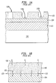
- FIG. 1A shows a cross-sectional view of a semiconductor substrate 100 having a developed photoresist layer 106.
- the semiconductor device 100 has a layer 102 that is the target for a subsequent etching operation.
- a conventional bottom anti-reflective layer (BARL) 104 is typically applied over the layer 102 to aid in suppressing reflective light and to better control "critical dimensions" (CDs).
- a positive DUV photoresist layer 106 is spin-coated over the BARL layer 104.
- a PEB operation is performed, and a development is performed, a poor resolution will unfortunately appear.
- the DUV photoresist 108 is shown having poor resolution that is a result of undeveloped photoresist material at regions 108a-108c.
- One of the resulting poor resolutions is believed to occur when an acid compound of the PAG is prematurely lost. This acid loss may be attributed to a number of well known factors, including, base neutralization, evaporation, or both. In some cases, the acid loss at the interface of air and photoresist is so severe that very poor resolution occurs as illustrated by region 108c.
- the poor resolution is sometimes referred to as "T-top"( i.e ., closed patterns for contact hole structures and bridged patterns for line/space structures). As a result, only surface skin of the DUV photoresist layer 106 is left at 108c.
- Acid loss will also occur at an interface 120 of the BARL layer 104 and the DUV photoresist layer 106, which is illustrated in Figure 1B due to "acid diffusion”and “acid neutralization.”
- Figure 1B therefore shows a number of acid diffusion arrow 130 that pictorially exhibit the loss of acid away from the DUV photoresist layer 106.
- scumming or "footing” will unfortunately occur at region 108a, and closed patterns may occur at resgion 108b.
- Another reason for poor resolution is caused by poor aerial imaging that results when light is diffracted as it passes through a stepper reticle.
- features having CDs of about 175 nm will unfortunately suffer from the increased light diffraction. Consequently, a poor aerial image of light is produced over the DUV photoresist layer 106, thereby decreasing the intensity of light that is needed to generate a strong acid to catalyze the deprotection reaction near the BARL layer 104 interface 120.
- regions near the interface of the DUV photoresist layer 106 and the anti-reflective layer 104 will not generate sufficient acid, and therefore less acid will be available to catalyze the deprotection groups of the polymer resin. Because the deprotection groups of the polymer resin are not sufficiently catalyzed, those regions of the DUV photoresist will remain in-soluble during the development stage, and regions 108a-c will remain in the developed photoresist. That is, only a part of the photoresist will become soluble during the development stage, thereby producing very poor feature resolution. Poor photoresist resolution is particularly problematic in view of continued demands for smaller integrated circuit feature sees.
- the present invention fills these needs by providing an enhanced anti-reflective layer that includes a predetermined amount of photo-acid generator (PAG) that is configured to off-set the DUV photoresist acid loss and insufficient light exposure.
- PAG photo-acid generator
- a method for making an anti-reflective layer for improving photoresist resolution and process window includes providing a first volume of organic anti-reflective chemical. Providing a second volume of photo-acid generator chemical. The second volume being between about 0.01 percent and about 30 percent of the first volume. Mixing the first volume of organic anti-reflective chemical and the second volume of photo-acid generator chemical substantially simultaneously to produce an enhanced anti-reflective chemical with an increased level of acid.
- a deep ultra-violet photolithography layered structure in another embodiment, includes a base layer that is selected for patterning.
- An enhanced anti-reflective layer that is composed of an organic polymer and a predetermined amount of added photo-acid generator.
- the layered structure also includes a deep ultra-violet photoresist overlying the enhanced anti-reflective layer.
- the deep ultra-violet photoresist includes a photo-acid generator component and an organic polymer resin component.
- a system for generating an anti-reflective layer for improving deep ultra-violet photoresist imaging and resolution includes providing a first volume of organic anti-reflective chemical. Providing a second volume of photo-acid generator chemical. The second volume being between about 0.1 percent and about 12 percent of the first volume. Means for mixing the first volume of organic anti-reflective chemical and the second volume of photo-acid generator chemical to produce an enhanced anti-reflective chemical with an increased level of acid.
- the aforementioned problems of photoresist footing and scumming are substantially eliminated due to the addition of a percentage of photo-acid generator into the organic polymer anti-reflective layer.
- a percentage of photo-acid generator into the organic polymer anti-reflective layer.
- FIG. 2 shows a cross-sectional view of a semiconductor substrate 200 having an overlying layer 102 in accordance with one embodiment of the present invention.
- semiconductor substrate 200 may be a portion of a silicon wafer, such as those commonly used in the fabrication of integrated circuits (ICs).
- ICs include random access memories (RAMs), dynamic random access memories (DRAMs), synchronous DRAMs (SDRAMs), and read only memories (ROMs).
- RAMs random access memories
- DRAMs dynamic random access memories
- SDRAMs synchronous DRAMs
- ROMs read only memories
- ICs such as application specific integrated circuits (ASICs), merge DRAM-logic (embedded DRAM) ICs or other logic circuits can also be fabricated.
- ASICs application specific integrated circuits
- merge DRAM-logic (embedded DRAM) ICs or other logic circuits can also be fabricated.
- a plurality of ICs are formed on the wafer in parallel. After processing is finish, the wafer is
- the chips are then packaged, resulting in a final product that is used in, for example, consumer products such as computer systems, cellular phones, personal digital assistants (PDAs), and other electronic products.
- the layer 202 may be any fabricated layer that may be deposited, sputtered, formed or applied to over the semiconductor substrate 200.
- the layer 202 is preferably well suited for patterning to define features of an integrated circuit design.
- layer 200 may be a dielectric layer, such as a silicon dioxide (SiO 2 ) layer that acts as an insulator between successive metallization layers.
- Layer 202 may also be aluminum, copper, or polysilicon which is commonly used to define transistor gates in a semiconductor circuit design. Accordingly, layer 202 should be understood to be any layer in an integrated circuit design that may require subsequent patterning through the use of a number of well known etching techniques.
- Figure 3 shows the cross-sectional view of Figure 2 after an enhanced anti-reflective layer 204 has been applied over the layer 202 in accordance with one embodiment of the present invention.
- the enhanced anti-reflective layer comprises photo-acid generator (PAG).
- the PAG generates acids during exposure, thereby increasing the acid concentration sufficiently at the interface of the resist bottom and ARC to compensate for acid loss in the interface and/or insufficient exposure.
- the acid combined with suitable bake temperature catalyzes the deprotection reaction of polymers, causing the polymers to be soluble in the base developer.
- the enhanced anti-reflective layer 204 is preferably a layer that is spin-coated in a similar manner as conventional organic anti-reflective layers are applied. Other suitable techniques of depositing the enhanced anti-reflective are also useful.
- the enhanced anti-reflective compound is provided by, for example, mixing an organic polymer liquid used to form an anti-reflective layer 204 with PAG. The amount of PAG is sufficient, when activated, to increase the concentration of acid in the enhanced anti-reflective layer to compensate for acid loss or insufficient acid. Insufficient amounts of acid cause, for example, resist footing.
- the organic polymer that makes up the enhanced anti-reflective layer 204 is mixed with between about 0.01 percent and about 30 percent (all percentages are by volume, unless noted otherwise).
- the enhanced anti-reflective layer 204 will have an increased PAG acid concentration that will advantageously limit the amount of acid that may diffuse from a subsequently deposited DUV photoresist layer.
- the PAG that is added to the organic polymer will preferably be substantially stable during high thermal process steps that are typically performed as part of post-apply bake (PAB) and post-exposed bake (PEB) operations.
- PAB post-apply bake
- PEB post-exposed bake
- a suitably stable PAG compound is preferably a Diphenyliodonium Salt or other well known PAG compounds.
- the PAB temperatures will range between about 80 degrees Celsius and about 150 degrees Celsius, and will most preferably be about 100 degrees Celsius.
- the PEB temperatures generally range between about 90 degrees Celsius and about 150 degrees Celsius, and will most preferably be about 135 degrees Celsius. Under these process conditions, the PAG component should remain thermally stable and should not react with the organic polymer of the enhanced anti-reflective layer 204.
- a preferred thickness for the enhanced anti-reflective layer 204 is between about 300 angstroms and about 2,000 angstroms, and more preferably between about 500 angstroms and about 900 angstroms, and most preferably about 1,000 angstroms.
- Figure 4 shows the cross-sectional view of Figure 3 after a DUV photoresist layer 206 has been spin-coated over the enhanced anti-reflective layer 204 in accordance with one embodiment of the present invention.
- the DUV photoresist is a "positive” photoresist which may be a "UV 2 HS", “UV 4 HS", “UV 6 HS” or any other suitable positive photoresist having a polymer resin component (i.e., as a matrix) and a photo-acid generator PAG) component.
- the DUV photoresist layer 206 is preferably spin coated to a thickness of between about 4,000 angstroms and about 15,000 angstroms, and more preferably between about 6,000 angstroms and about 7,000 angstroms, and most preferably about 6,500 angstroms.
- the wafer is preferably subjected to a post-apply bake (PAB) on a hot plate to drive the solvent and ensure that the photoresist material is sufficiently hard before being exposed.
- PAB post-apply bake
- the wafer is moved to a stepper apparatus, which is used to expose selected portions of the DUV photoresist layer 206 to DUV wavelength (e.g ., 248 nm or 193 nm) light 400.
- the stepper apparatus has a reticle that includes the desired patterns that are to be transferred onto the DUV photoresist layer 206 with the aid of DUV wavelength light 400.
- the exposed regions generate a strong acid 402.
- the enhanced anti-reflective layer 204 contains a percentage of PAG, those regions of the DUV photoresist layer 206 that are at the interface with the enhanced anti-reflective layer 204 will have a relatively high concentration of acid, thereby effectively countering acid diffusion effects and poor aerial image. Accordingly, because more acid is generated at this interface, the scumming and footing may no longer be present in the developed DUV photoresist layer 206.
- the semiconductor wafer is moved onto a hot plate where a post-exposure bake (PEB) is performed at a temperature of between about 150 degrees Celsius and about 250 degrees Celsius, which causes the strong acid 402 to catalyze deep protection groups of the polymer resin that are contained in the DUV photoresist layer 206.
- PEB post-exposure bake
- the deprotection groups of the polymer resin catalyze much more uniformly down to the underlying enhanced anti-reflective layer 204.
- those exposed portions of the DUV photoresist layer 206 will now become "soluble" to a developer, which is typically an aqueous base solution.
- the DUV photoresist layer 206 will have developed regions 208a-208b that extend substantially down to the enhanced anti-reflective layer 204, as shown in Figure 5.
- regions 208a-208b that extend substantially down to the enhanced anti-reflective layer 204, as shown in Figure 5.
- diffusion of acid out of the DUV photoresist layer 206 and to the underlying enhanced anti-reflective layer 204 will be substantially reduced. That is, although some acid diffusion is still present, the acid loss problem will be substantially eliminated. As such, the problematic resolution issues created by acid loss are substantially cured, thereby enabling the fabrication of photoresist masks that provide improved aspect ratios.
- Figure 6 is a flowchart diagram illustrating the preferred method operations in accordance with one embodiment of the present invention.
- the method begins at an operation 602 where a layer is provided for photolithography patterning.
- the layer may be any layer such as an oxide layer, a metallization layer, silicon layer, polysilicon layer, etc. As is well known, these layers are commonly patterned to form numerous features that make up integrated circuit designs that are fabricated to make semiconductor chips.
- the method proceeds to an operation 604 where an anti-reflective chemical is provided.
- the anti-reflective chemical is an organic polymer which is typically used as a bottom anti-reflective layer (BARL).
- BARL bottom anti-reflective layer
- the method proceeds to an operation 606 where a photo-acid generator (PAG) chemical is provided.
- PAG photo-acid generator
- the PAG is preferably a Diphenyliodonium Salt or other suitable PAG compound that is thermally stable during the bake operations and does not react with the polymer of the anti-reflective layer.
- the method then proceeds to an operation 608 where the anti-reflective chemical and a percentage of the PAG is substantially simultaneously mixed to produce an enhance anti-reflective chemical.
- a percentage of between about 0.01% and about 30% PAG of the volume of the anti-reflective chemical is provided to produce the enhanced anti-reflective chemical.
- the method proceeds to an operation 606 where the enhanced anti-reflective chemical is spin-coated over the layer provided for photolithography patterning in operation 602.
- the enhanced anti-reflective layer will have a thickness of between about 300 angstroms and about 2,000 angstroms.
- the method proceeds to an operation 612 where a deep ultra-violet (DUV) photoresist is applied over the spin-coated enhanced anti-reflective layer as described above.
- DUV deep ultra-violet
- the spin coated DUV photoresist has a thickness of between about 4,000 angstrom and about 15,000 angstroms.
- the wafer on which the DUV photoresist is spin-coated is placed on a hot plate to perform a post-apply bake (PAB), such that the DUV photoresist hardens.
- PAB post-apply bake
- the method then proceeds to an operation 614 where selected regions of the DUV photoresist are exposed.
- the exposed regions will produce a strong acid that will assist in catalyzing the deprotection groups of the polymer resin of the DUV photoresist layer when the exposed DUV photoresist layer is subjected to a post-exposed bake (PEB).
- PEB post-exposed bake
- the method then proceeds to an operation 616 where the DUV photoresist is developed in an aqueous base solution that substantiallly removes all exposed regions of the DUV photoresist.
Landscapes
- Engineering & Computer Science (AREA)
- Physics & Mathematics (AREA)
- General Physics & Mathematics (AREA)
- Manufacturing & Machinery (AREA)
- Structural Engineering (AREA)
- Condensed Matter Physics & Semiconductors (AREA)
- Architecture (AREA)
- Computer Hardware Design (AREA)
- Microelectronics & Electronic Packaging (AREA)
- Power Engineering (AREA)
- Materials For Photolithography (AREA)
- Exposure Of Semiconductors, Excluding Electron Or Ion Beam Exposure (AREA)
- Photosensitive Polymer And Photoresist Processing (AREA)
- Exposure And Positioning Against Photoresist Photosensitive Materials (AREA)
Abstract
Description
Claims (25)
- A method for making an anti-reflective layer for improving photoresist resolution and process window, comprising:providing a first volume of organic anti-reflective chemical;providing a second volume of photo-acid generator chemical, the second volume being between about 0.01 percent and about 30 percent of the first volume;mixing the first volume of organic anti-reflective chemical and the second volume of photo-acid generator chemical substantially simultaneously to produce an enhanced anti-reflective chemical with an increased level of acid.
- A method for making an anti-reflective layer for improving photoresist resolution and process window as recited in claim 1, wherein the photo-acid generator is thermally stable.
- A method for making an anti-reflective layer for improving photoresist resolution and process window as recited in claim 2, further comprising:spin-coating the enhanced anti-reflective chemical over a layer that is selected to be patterned, the spin-coating being configured to produce an enhanced anti-reflective layer.
- A method for making an anti-reflective layer for improving photoresist resolution and process window as recited in claim 3, further comprising:spin-coating a deep ultra-violet photoresist layer over the spin-coated enhanced anti-reflective layer, the deep ultra-violet photoresist layer includes an organic polymer resin component and a photo-acid generator component.
- A method for making an anti-reflective layer for improving photoresist resolution and process window as recited in claim 4, wherein the organic polymer resin includes deprotection groups.
- A method for making an anti-reflective layer for improving photoresist resolution and process window as recited in claim 5, wherein the increased level of acid of the enhanced anti-reflective layer substantially reduces diffusion of the photo-acid generator component and acid of the deep ultra-violet photoresist layer into the enhanced anti-reflective layer.
- A method for making an anti-reflective layer for improving photoresist resolution and process window as recited in claim 6, wherein the deep ultra-violet photoresist layer is a positive photoresist.
- A method for making an anti-reflective layer for improving photoresist resolution and process window as recited in claim 7, further comprising:exposing a light energy onto selected regions of the deep ultra-violet photoresist layer, the exposed regions being configured to produce a strong acid.
- A method for making an anti-reflective layer for improving photoresist resolution and process window as recited in claim 8, further comprising:subjecting the produced strong acid to a post-expose bake temperature ranging between about 90 degrees Celsius and about 150 degrees Celsius, the post-expose bake temperature being configured to cause the strong acid to catalyze the deprotection groups of the organic polymer resin.
- A method for making an anti-reflective layer for improving photoresist resolution and process window as recited in claim 9, wherein the light energy has wavelengths of between about 248 nm and 193 nm.
- A deep ultra-violet photolithography layered structure, comprising:a base layer that is selected for patterning;an enhanced anti-reflective layer that is composed of an organic polymer and a predetermined amount of added photo-acid generator; anda deep ultra-violet photoresist overlying the enhanced anti-reflective layer, the deep ultra-violet photoresist includes a photo-acid generator component and an organic polymer resin component.
- A deep ultra-violet photolithography layered structure as recited in claim 11, wherein the organic polymer resin component includes deprotection groups.
- A deep ultra-violet photolithography layered structure as recited in claim 12, wherein the predetermined amount of added photo-acid generator is between about 0.01 percent and about 30 percent of the organic polymer.
- A deep ultra-violet photolithography layered structure as recited in claim 12, wherein the predetermined amount of added photo-acid generator is between about 0.1 percent and about 6 percent of the organic polymer.
- A deep ultra-violet photolithography layered structure as recited in claim 14, wherein the enhanced anti-reflective layer is between about 300 angstroms and about 2,000 angstroms.
- A deep ultra-violet photolithography layered structure as recited in claim 14, wherein the deep ultra-violet photoresist has a thickness of between about 4,000 angstroms and about 15,000 angstroms.
- A deep ultra-violet photolithography layered structure as recited in claim 16, wherein a deep ultra-violet wavelength selected from a 248 nm wavelength and a 193 nm wavelength is used to generate a strong acid in exposed regions of the deep ultra-violet photoresist.
- A deep ultra-violet photolithography layered structure as recited in claim 17, wherein a hot plate is used to heat the generated strong acid of the exposed regions, the heat being configured to catalyze the deprotection groups of the organic polymer resin component.
- A deep ultra-violet photolithography layered structure as recited in claim 18, wherein the deprotection groups of the organic polymer catalyze down to the base layer that is selected for patterning, such that scumming and footing is eliminated after a photoresist development stage is complete.
- A system for generating an anti-reflective layer for improving deep ultra-violet photoresist imaging resolution and process window, comprising:providing a first volume of organic anti-reflective chemical;providing a second volume of photo-acid generator chemical, the second volume being between about 0.01 percent and about 12 percent of the first volume;means for mixing the first volume of organic anti-reflective chemical and the second volume of photo-acid generator chemical to produce an enhanced anti-reflective chemical with an increased level of acid.
- A system for generating an anti-reflective layer for improving deep ultra-violet photoresist imaging resolution and process window as recited in claim 20, further comprising:spin-coating the enhanced anti-reflective chemical over a base layer that is selected to be patterned, the spin-coating being configured to produce an enhanced anti-reflective layer; andspin-coating a deep ultra-violet photoresist layer over the spin-coated enhanced anti-reflective layer, the deep ultra-violet photoresist layer includes an organic polymer resin component and a photo-acid generator component.
- A system for generating an anti-reflective layer for improving deep ultra-violet photoresist imaging resolution and process window as recited in claim as recited in claim 21, wherein the organic polymer resin includes deprotection groups.
- A system for generating an anti-reflective layer for improving deep ultra-violet photoresist imaging resolution and process window as recited in claim 22, wherein the increased level of acid of the enhanced anti-reflective layer substantially reduces diffusion of the photo-acid generator component and acid of the deep ultra-violet photoresist layer into the enhanced anti-reflective layer.
- A system for generating an anti-reflective layer for improving deep ultra-violet photoresist imaging resolution, and process window as recited in claim 22, wherein a developing time and developer is reduced.
- A system for generating an anti-reflective layer for improving deep ultra-violet photoresist imaging resolution, and process window as recited in claim 22, wherein a substrate contaminating effect that poisons the deep ultra-violet photoresist layer is minimized.
Applications Claiming Priority (2)
| Application Number | Priority Date | Filing Date | Title |
|---|---|---|---|
| US94080597A | 1997-09-30 | 1997-09-30 | |
| US940805 | 1997-09-30 |
Publications (1)
| Publication Number | Publication Date |
|---|---|
| EP0905565A1 true EP0905565A1 (en) | 1999-03-31 |
Family
ID=25475450
Family Applications (1)
| Application Number | Title | Priority Date | Filing Date |
|---|---|---|---|
| EP98115794A Withdrawn EP0905565A1 (en) | 1997-09-30 | 1998-08-21 | Improved deep ultraviolet photolithography |
Country Status (5)
| Country | Link |
|---|---|
| EP (1) | EP0905565A1 (en) |
| JP (1) | JPH11162846A (en) |
| KR (1) | KR100581450B1 (en) |
| CN (1) | CN1182440C (en) |
| TW (1) | TW398030B (en) |
Cited By (14)
| Publication number | Priority date | Publication date | Assignee | Title |
|---|---|---|---|---|
| EP1065568A2 (en) * | 1999-07-02 | 2001-01-03 | Asm Lithography B.V. | EUV-Lithographic projection apparatus comprising an optical element with a capping layer |
| US6411604B1 (en) | 1998-06-05 | 2002-06-25 | Inet Technologies, Inc. | System and method for correlating transaction messages in a communications network |
| WO2002091080A1 (en) * | 2001-05-03 | 2002-11-14 | Applied Materials, Inc. | Organic bottom antireflective coating for high performance mask making optical imaging |
| WO2003010601A1 (en) * | 2001-07-23 | 2003-02-06 | Applied Materials, Inc. | Method of preparing optically imaged high performance photomasks |
| US6529594B1 (en) | 1998-06-05 | 2003-03-04 | Inet Technologies, Inc. | System and method for generating quality of service statistics for an international communications network |
| WO2003057678A1 (en) * | 2002-01-09 | 2003-07-17 | Clariant International Ltd | Positive-working photoimageable bottom antireflective coating |
| US6753258B1 (en) | 2000-11-03 | 2004-06-22 | Applied Materials Inc. | Integration scheme for dual damascene structure |
| US7070914B2 (en) | 2002-01-09 | 2006-07-04 | Az Electronic Materials Usa Corp. | Process for producing an image using a first minimum bottom antireflective coating composition |
| US7115534B2 (en) | 2003-05-19 | 2006-10-03 | Applied Materials, Inc. | Dielectric materials to prevent photoresist poisoning |
| US7160665B2 (en) * | 2002-12-30 | 2007-01-09 | International Business Machines Corporation | Method for employing vertical acid transport for lithographic imaging applications |
| EP1742108A1 (en) * | 2005-07-05 | 2007-01-10 | Rohm and Haas Electronic Materials, L.L.C. | Coating compositions for use with an overcoated photoresist |
| EP1813986A2 (en) | 2006-01-29 | 2007-08-01 | Rohm and Haas Electronic Materials, L.L.C. | Coating compositions for use with an overcoated photoresist |
| EP1939688A1 (en) * | 2005-09-27 | 2008-07-02 | Nissan Chemical Industries, Ltd. | Composition for antireflection film formation, comprising product of reaction between isocyanuric acid compound and benzoic acid compound |
| CN104733290A (en) * | 2013-12-19 | 2015-06-24 | 中芯国际集成电路制造(上海)有限公司 | Coating method for bottom anti-reflective coating |
Families Citing this family (3)
| Publication number | Priority date | Publication date | Assignee | Title |
|---|---|---|---|---|
| CN100449711C (en) * | 2006-04-03 | 2009-01-07 | 中芯国际集成电路制造(上海)有限公司 | Forming method for metal silicide blocking area and method for producing semiconductor device |
| JP5112733B2 (en) * | 2006-04-11 | 2013-01-09 | ローム・アンド・ハース・エレクトロニック・マテリアルズ,エル.エル.シー. | Coating composition for photolithography |
| US8871423B2 (en) | 2010-01-29 | 2014-10-28 | Samsung Electronics Co., Ltd. | Photoresist composition for fabricating probe array, method of fabricating probe array using the photoresist composition, composition for photosensitive type developed bottom anti-reflective coating, fabricating method of patterns using the same and fabricating method of semiconductor device using the same |
Citations (2)
| Publication number | Priority date | Publication date | Assignee | Title |
|---|---|---|---|---|
| EP0542008A1 (en) * | 1991-11-15 | 1993-05-19 | Shipley Company Inc. | Antihalation compositions |
| US5324550A (en) * | 1992-08-12 | 1994-06-28 | Hitachi, Ltd. | Pattern forming method |
-
1998
- 1998-08-11 CN CNB981162754A patent/CN1182440C/en not_active Expired - Fee Related
- 1998-08-21 EP EP98115794A patent/EP0905565A1/en not_active Withdrawn
- 1998-09-02 TW TW087114540A patent/TW398030B/en not_active IP Right Cessation
- 1998-09-25 JP JP10271806A patent/JPH11162846A/en not_active Withdrawn
- 1998-09-29 KR KR1019980040452A patent/KR100581450B1/en not_active IP Right Cessation
Patent Citations (2)
| Publication number | Priority date | Publication date | Assignee | Title |
|---|---|---|---|---|
| EP0542008A1 (en) * | 1991-11-15 | 1993-05-19 | Shipley Company Inc. | Antihalation compositions |
| US5324550A (en) * | 1992-08-12 | 1994-06-28 | Hitachi, Ltd. | Pattern forming method |
Cited By (28)
| Publication number | Priority date | Publication date | Assignee | Title |
|---|---|---|---|---|
| US6529594B1 (en) | 1998-06-05 | 2003-03-04 | Inet Technologies, Inc. | System and method for generating quality of service statistics for an international communications network |
| US6411604B1 (en) | 1998-06-05 | 2002-06-25 | Inet Technologies, Inc. | System and method for correlating transaction messages in a communications network |
| US6724462B1 (en) | 1999-07-02 | 2004-04-20 | Asml Netherlands B.V. | Capping layer for EUV optical elements |
| EP1065568A3 (en) * | 1999-07-02 | 2003-03-19 | ASML Netherlands B.V. | EUV-Lithographic projection apparatus comprising an optical element with a capping layer |
| USRE42338E1 (en) | 1999-07-02 | 2011-05-10 | Asml Netherlands B.V. | Capping layer for EUV optical elements |
| US6738188B2 (en) | 1999-07-02 | 2004-05-18 | Asml Netherlands B.V. | Multilayer extreme ultraviolet mirrors with enhanced reflectivity |
| EP1065568A2 (en) * | 1999-07-02 | 2001-01-03 | Asm Lithography B.V. | EUV-Lithographic projection apparatus comprising an optical element with a capping layer |
| US6753258B1 (en) | 2000-11-03 | 2004-06-22 | Applied Materials Inc. | Integration scheme for dual damascene structure |
| WO2002091080A1 (en) * | 2001-05-03 | 2002-11-14 | Applied Materials, Inc. | Organic bottom antireflective coating for high performance mask making optical imaging |
| US6605394B2 (en) | 2001-05-03 | 2003-08-12 | Applied Materials, Inc. | Organic bottom antireflective coating for high performance mask making using optical imaging |
| WO2003010601A1 (en) * | 2001-07-23 | 2003-02-06 | Applied Materials, Inc. | Method of preparing optically imaged high performance photomasks |
| US6703169B2 (en) | 2001-07-23 | 2004-03-09 | Applied Materials, Inc. | Method of preparing optically imaged high performance photomasks |
| US6998206B2 (en) | 2001-07-23 | 2006-02-14 | Applied Materials, Inc. | Method of increasing the shelf life of a blank photomask substrate |
| US7070914B2 (en) | 2002-01-09 | 2006-07-04 | Az Electronic Materials Usa Corp. | Process for producing an image using a first minimum bottom antireflective coating composition |
| WO2003057678A1 (en) * | 2002-01-09 | 2003-07-17 | Clariant International Ltd | Positive-working photoimageable bottom antireflective coating |
| US6844131B2 (en) | 2002-01-09 | 2005-01-18 | Clariant Finance (Bvi) Limited | Positive-working photoimageable bottom antireflective coating |
| US7160665B2 (en) * | 2002-12-30 | 2007-01-09 | International Business Machines Corporation | Method for employing vertical acid transport for lithographic imaging applications |
| US7585609B2 (en) | 2002-12-30 | 2009-09-08 | International Business Machines Corporation | Bilayer film including an underlayer having vertical acid transport properties |
| US7115534B2 (en) | 2003-05-19 | 2006-10-03 | Applied Materials, Inc. | Dielectric materials to prevent photoresist poisoning |
| US7585612B2 (en) | 2005-07-05 | 2009-09-08 | Rohm And Haas Electronic Materials Llc | Coating compositions for use with an overcoated photoresist |
| EP1742108A1 (en) * | 2005-07-05 | 2007-01-10 | Rohm and Haas Electronic Materials, L.L.C. | Coating compositions for use with an overcoated photoresist |
| EP1939688A4 (en) * | 2005-09-27 | 2010-06-02 | Nissan Chemical Ind Ltd | Composition for antireflection film formation, comprising product of reaction between isocyanuric acid compound and benzoic acid compound |
| EP1939688A1 (en) * | 2005-09-27 | 2008-07-02 | Nissan Chemical Industries, Ltd. | Composition for antireflection film formation, comprising product of reaction between isocyanuric acid compound and benzoic acid compound |
| EP1813986A3 (en) * | 2006-01-29 | 2008-11-05 | Rohm and Haas Electronic Materials, L.L.C. | Coating compositions for use with an overcoated photoresist |
| EP1813986A2 (en) | 2006-01-29 | 2007-08-01 | Rohm and Haas Electronic Materials, L.L.C. | Coating compositions for use with an overcoated photoresist |
| CN101017326B (en) * | 2006-01-29 | 2011-10-12 | 罗门哈斯电子材料有限公司 | Coating compositions for use with an overcoated photoresist |
| CN104733290A (en) * | 2013-12-19 | 2015-06-24 | 中芯国际集成电路制造(上海)有限公司 | Coating method for bottom anti-reflective coating |
| CN104733290B (en) * | 2013-12-19 | 2017-11-24 | 中芯国际集成电路制造(上海)有限公司 | The painting method of bottom antireflective coating |
Also Published As
| Publication number | Publication date |
|---|---|
| KR100581450B1 (en) | 2006-07-25 |
| JPH11162846A (en) | 1999-06-18 |
| CN1182440C (en) | 2004-12-29 |
| TW398030B (en) | 2000-07-11 |
| KR19990030227A (en) | 1999-04-26 |
| CN1213789A (en) | 1999-04-14 |
Similar Documents
| Publication | Publication Date | Title |
|---|---|---|
| US6313492B1 (en) | Integrated circuit chip produced by using frequency doubling hybrid photoresist | |
| EP0905565A1 (en) | Improved deep ultraviolet photolithography | |
| US5593725A (en) | Anti-reflective layer and method for manufacturing semiconductor device using the same | |
| TWI449084B (en) | Methods of forming electronic devices | |
| US5652084A (en) | Method for reduced pitch lithography | |
| US4745042A (en) | Water-soluble photopolymer and method of forming pattern by use of the same | |
| US6180320B1 (en) | Method of manufacturing a semiconductor device having a fine pattern, and semiconductor device manufactured thereby | |
| EP2089770B1 (en) | Method of creating photolithographic structures with developer-trimmed hard mask | |
| CN101335198B (en) | Method for forming fine pattern of semiconductor device | |
| US20060160028A1 (en) | Method of forming fine patterns of a semiconductor device | |
| US6184041B1 (en) | Fused hybrid resist shapes as a means of modulating hybrid resist space width | |
| JP2000315647A (en) | Formation of resist pattern | |
| US9058997B2 (en) | Process of multiple exposures with spin castable films | |
| EP1478978B1 (en) | Self-aligned pattern formation using dual wavelengths | |
| US5512422A (en) | Method of forming resist pattern and organic silane compound for forming anti-reflection film for use in such method | |
| US6171761B1 (en) | Resist pattern forming method utilizing multiple baking and partial development steps | |
| US5648199A (en) | Method of forming a resist pattern utilizing an acid water-soluble material overlayer on the resist film | |
| JPH0786127A (en) | Formation of resist pattern | |
| EP0449272B1 (en) | Pattern forming process | |
| JP2560773B2 (en) | Pattern formation method | |
| BE1014248A3 (en) | Method for producing a printed circuit used for manufacturing semiconductor device. | |
| JP2692241B2 (en) | Method of forming resist pattern | |
| US20240004302A1 (en) | Method of manufacturing semiconductor device | |
| Amblard et al. | Advanced i-line lithography: processes for positive and negative patterning using the same acid hardening resist | |
| JPH0433325A (en) | Photo etching for forming fine pattern |
Legal Events
| Date | Code | Title | Description |
|---|---|---|---|
| PUAI | Public reference made under article 153(3) epc to a published international application that has entered the european phase |
Free format text: ORIGINAL CODE: 0009012 |
|
| AK | Designated contracting states |
Kind code of ref document: A1 Designated state(s): DE FR GB IE IT NL |
|
| AX | Request for extension of the european patent |
Free format text: AL;LT;LV;MK;RO;SI |
|
| 17P | Request for examination filed |
Effective date: 19990601 |
|
| AKX | Designation fees paid |
Free format text: DE FR GB IE IT NL |
|
| 17Q | First examination report despatched |
Effective date: 20001211 |
|
| RAP1 | Party data changed (applicant data changed or rights of an application transferred) |
Owner name: INFINEON TECHNOLOGIES AG |
|
| REG | Reference to a national code |
Ref country code: HK Ref legal event code: WD Ref document number: 1017441 Country of ref document: HK |
|
| STAA | Information on the status of an ep patent application or granted ep patent |
Free format text: STATUS: THE APPLICATION IS DEEMED TO BE WITHDRAWN |
|
| 18D | Application deemed to be withdrawn |
Effective date: 20070226 |