-
This invention relates to organic electroluminescent (EL) devices.
More specifically, this invention relates to electroluminescent devices with efficient
electron transport.
-
Organic EL devices are known to be highly efficient and are capable
of producing a wide range of colors. Useful applications such as flat-panel displays
have been contemplated. Representative of earlier organic EL devices are US-A-3,172,862,
US-A-3,173,050, "Double Injection Electroluminescence in
Anthracene," RCA Review, Vol. 30, pp. 322-334, 1969; and US-A-3,710,167.
Typical organic emitting materials were formed of a conjugated organic host
material and a conjugated organic activating agent having condensed benzene
rings. The organic emitting material was present as a single layer medium having a
thickness much above 1 micrometer. Thus, this organic EL medium was highly
resistive and the EL device required an extremely high voltage (>100 volts) to
operate.
-
The most recent discoveries in the art of organic EL device
construction have resulted in devices having the organic EL medium consisting of
extremely thin layers (<1.0 micrometer in combined thickness) separating the
anode and cathode. The thin organic EL medium offers reduced resistance,
permitting higher current densities for a given level of electrical bias voltage. In a
basic two-layer EL device structure, one organic layer is specifically chosen to
inject and transport holes and the other organic layer is specifically chosen to inject
and transport electrons. The interface between the two layers provides an efficient
site for the recombination of the injected hole-electron pair and resultant
electroluminescence. Examples are provided by US-A-4,356,429; US-A-4,539,507;
US-A-4,720,432; US-A-4,885,211; US-A-4,950,950; US-A-5,047,687;
US-A-5,059,861; US-A-5,061,569; US-A-5,073,446; US-A-5,141,671;
US-A-5,150,006 and US-A-5,151,629.
-
The simple structure can be modified to a three-layer structure, in
which an additional luminescent layer is introduced between the hole and electron
transporting layers to function primarily as the site for hole-electron recombination
and thus electroluminescence. In this respect, the functions of the individual
organic layers are distinct and can therefore be optimized independently. Thus, the
luminescent or recombination layer can be chosen to have a desirable EL color as
well as a high luminance efficiency. Likewise, the electron and hole transport
layers can be optimized primarily for the carrier transport property.
One inherent drawback of the organic EL devices is that the mobility of electrons
in organic materials is extremely low, so that a high voltage is required to produce
a strong electric field. For instance, the mobility of electrons in Alq is in the range
of 10-6-10-7 cm2/V·S, and thus a field of 1×10⁶ V/cm is necessary for efficient
electron transport. The thickness of the organic medium can be reduced to lower
the voltage level required for device operation, however, the reduction results in
low quantum efficiency due to the effect of radiative quenching by a conducting
surface, high leakage current, or device shorting.
-
It is an object of the present invention to provide an organic EL
device with efficient electron transport.
-
The above object is achieved in an organic EL device, comprising
an anode, an organic hole transporting layer over the anode, an organic
luminescent layer on the organic hole transporting layer, an inorganic electron
transporting layer over the organic luminescent layer, and a cathode on the electron
transporting layer.
-
The new device exhibits superior current-voltage and luminescence-voltage
characteristics over a conventional EL device with an organic electron
transporting layer.
-
These and other advantages of this invention can be better
appreciated by reference to the following detailed description considered in
conjunction with the drawings in which:
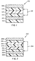
- FIG. 1 is a schematic diagram of an embodiment of the multi-layer
structures of EL devices in accordance with the present invention;
- FIG. 2 is a schematic diagram of an another embodiment of the
multi-layer structures of EL devices in accordance with the present invention;
- FIG. 3 shows plots of current-voltage characteristics for a
conventional device and the device schematically shown in FIG. 2; and
- FIG. 4 shows plots of luminescence-voltage characteristics for a
conventional device and the device shown in FIG. 2.
-
-
An EL device 100 according to the invention is schematically
illustrated in FIG. 1. The support layer 102 is an electrically insulating and an
optically transparent material such as glass or plastic. Anode 104 is separated from
cathode 106 by an EL medium 108, which, as shown, includes three superimposed
layers. Layer 110 adjacent to anode 104 is the hole transporting layer. Layer 114
adjacent to cathode 106 is the electron transporting layer. Layer 112 which is in
between the hole transporting layer 110 and the electron transporting layer 114 is
the luminescent layer. This luminescent layer 112 also serves as the recombination
layer where the hole and electron recombines. In the present invention both hole
transporting layer 110 and luminescent layer 112 are formed of organic materials,
while electron transporting layer 114 is formed of inorganic materials. The
electron transporting layer 114 can be formed on the luminescent layer 112 as
shown in FIG. 1 or over the luminescent layer 112 as will be discussed in FIG. 2.
The anode and the cathode are connected to an external AC or DC power source
(not shown). The power source can be pulsed, periodic, or continuous.
-
In operation, the EL device 100 can be viewed as a diode which is
forward biased when the anode is at a higher potential than the cathode. Under
these conditions, holes (positive charge carriers) are injected from the anode into
the hole transporting layer 110, and electrons are injected into the electron
transporting layer 114. The injected holes and electrons each migrate toward the
oppositely charged electrode. This results in hole-electron recombination and a
release of energy in part as light, thus producing electroluminescence.
-
Organic device 200 is illustrative of yet another preferred
embodiment of the present invention. The insulating and transparent support is
layer 202. The anode 204 is separated from the cathode 206 by an EL medium
208, which, as shown, includes five superimposed layers. Located on top of the
anode layer 204 are, in sequence, the organic hole injecting layer 210, the organic
hole transporting layer 212, the organic luminescent layer 214, the fluoride layer
216, and the inorganic electron transporting layer 218. The structure of device 200
is similar to device 100, except that a thin fluoride layer 216 is added to improve
the efficiency of electron transport from the electron transporting layer 218 into the
luminescent layer 214.
-
A substrate 102 and 202 for the EL devices 100 and 200,
respectively, is electrically insulating and light transparent. The light transparent
property is desirable for viewing the EL emission through the substrate. For
applications where the EL emission is viewed through the top electrode, the
transmissive characteristic of the support is immaterial, and therefore any
appropriate substrate such as opaque semiconductor and ceramic wafers can be
used. Of course, it is necessary to provide in these device configurations a light
transparent top electrode.
-
The composition of the EL medium is described as follows, with
particular reference to device structure 200.
-
A layer containing a porphyrinic compound forms the hole injecting
layer of the organic EL device. A porphyrinic compound is any compound, natural
or synthetic, which is derived from or includes a porphyrin structure, including
porphine itself. Any of the prophyrinic compounds disclosed in US-A-3,935,031
or US-A-4,356,429, the disclosures of which are here incorporated by reference,
can be employed.
-
The hole transporting layer of the organic EL device contains at
least one hole transporting aromatic tertiary amine, where the latter is understood
to be a compound containing at least one trivalent nitrogen atom that is bonded
only to carbon atoms, at least one of which is a member of an aromatic ring. In
one form the aromatic tertiary amine can be an arylamine, such as a monarylamine,
diarylamine, triarylamine, or a polymeric arylamine. Exemplary monomeric
triarylamines are illustrated in US-A-3,180,730. Other suitable triarylamines
substituted with vinyl or vinyl radicals and/or containing at least one active
hydrogen containing group are disclosed in US-A-3,567,450 and US-A-3,658,520.
-
The luminescent layer of the organic EL device comprises of a
luminescent or fluorescent material where electroluminescence is produced as a
result of electron-hole pair recombination in this region. In the simplest
construction, the luminescent layer comprises of a single component, that is a pure
material with a high fluorescent efficiency. A well known material is tris
(8-quinolinato) Aluminum, (Alq), which produces excellent green
electroluminescence. A preferred embodiment of the luminescent layer comprises a
multi-component material consisting of a host material doped with one or more
components of fluorescent dyes. Using this method, highly efficient EL devices
can be constructed. Simultaneously, the color of the EL devices can be tuned by
using fluorescent dyes of different emission wavelengths in a common host
material. This dopant scheme has been described in considerable details for EL
devices using Alq as the host material by Tang and others, J. Applied Physics, Vol.
65, Pages 3610-3616, 1989; US-A-4,769,292.
-
The inorganic electron transporting layer is an essential part in this
invention. Preferred materials for use in forming the electron transporting layer are
inorganic n-type semiconducting materials. The materials should have a resistivity
in the range of 1-105 ohm-cm, be transmissive or semi-transitive to visible light,
and be inert with respect to the organic luminescent layer.
-
An important relationship for choosing an inorganic semiconducting
material to form the electron transporting layer on an organic luminescent layer is
the comparison of the electron affinity of the inorganic material and the energy
level of the lowest unoccupied molecular orbital (ELUMO) of the organic material.
The electron affinity should not be greater than the ELUMO by 1.5 eV in order to
achieve efficient electron transport.
-
The inorganic semiconducting materials can be a metal oxide, metal
nitride, zinc sulfide, zinc selenide, or zinc telluride. For those materials, the
electron mobility is several orders of magnitude greater than that in organic
materials and the resistivity can be readily adjusted by impurity doping or
controlling ambient. Examples described in this invention indicate that zinc oxide
and indium oxide are suitable materials. Other materials can be titanium oxide,
strontium titanium oxide, barium titanium oxide, gallium nitride, or indium gallium
nitride.
-
The thickness of the inorganic layer is so selected that it would
provide a sufficient space separation between the luminescent layer and the top
cathode. A useful range of the thickness is from 20 to 2,000 nm, preferably 50-500
nm. This inorganic layer can be deposited by many conventional means, such as
evaporation, sputtering, laser ablation, and chemical vapor deposition.
-
The fluoride layer has an important contribution to this invention.
The presence of a fluoride on the luminescent layer results in band bending, thus
substantially lowering the barrier height for electron transport at the interface
between the electron transporting layer and the luminescent layer. The fluoride
layer used for band bending can be selected from an alkali fluoride or an alkaline
earth fluoride, which include lithium fluoride, sodium fluoride, potassium fluoride,
rubidium fluoride, cesium fluoride, magnesium fluoride, calcium fluoride, strontium
fluoride, or barium fluoride.
-
The anode and cathode of the organic EL device can each take any
convenient conventional form. Where it is intended to transmit light from the
organic EL device through the anode, this can be conveniently achieved by coating
a thin conductive layer onto a light transparent substrate-for example, a
transparent or substantially transparent glass plate or plastic film. In one form the
organic EL devices of this invention can follow the conventional practice of
including a light transparent anode formed of tin oxide or indium tin oxide coated
on a glass plate, as disclosed in US-A-3,172,862, US-A-3,173,050, Dresner
"Double Injection Electroluminescence in Anthracene", RCA Review, Volume 30,
pages 322-334, 1969; and US-A-3,710,167 cited above.
-
The organic EL devices of this invention can employ a cathode
constructed of any metal, including any high or low work function metal,
heretofore taught to be useful for this purpose. Unexpected fabrication,
performance, and stability advantages have been realized by forming the cathode of
a combination of a low work function metal and at least one other metal. For
further disclosure, see US-A-4,885,21, the disclosure of which is incorporated by
reference herein. A bilayer structure of LiF/Al has been used to enhance electron
injection, as disclosed in US-A-5,624,604.
Examples
-
The invention and its advantages are further illustrated by the
specific examples as follows:
Example 1
-
An EL device satisfying the requirements of the invention was
constructed in the following manner. The EL medium has four organic layers,
namely, a hole injecting layer, a hole transporting layer, a luminescent layer, and an
electron transporting layer
- a) An indium-tin-oxide (ITO) coated glass substrate was
sequentially ultrasonicated in a commercial detergent, rinsed in deionized water,
degreased in toluene vapor and exposed to oxygen plasma for a few minutes.
- b) A hole injecting layer of copper phthalocyanine (150
Angstroms) was then deposited on top of the ITO coated substrate by evaporation
from a tantalum boat.
- c) Onto the copper phthalocyanine layer was deposited a hole
transporting layer of N,N'-bis-(1-naphthyl)-N,N'-diphenylbenzidine (600
Angstroms), also by evaporation from a tantalum boat.
- d) A luminescent layer of Alq doped with 1% coumarin 6 ( 300
Angstroms) was then deposited onto the hole transporting layer by evaporation
from a tantalum boat.
- e) An electron transporting layer of Alq (450 Angstroms) was
then deposited onto the luminescent layer by evaporation from a tantalum boat.
- f) On top of the Alq layer was deposited by evaporation a
cathode layer (2000 Angstroms) formed of a 10:1 atomic ratio of Mg and Ag.
-
-
The above sequence completed the deposition of the EL device.
The device was then hermetically packaged in a dry glove box for protection
against ambient environment.
-
The drive voltage was 12.3 V at a current density of 100 mA/cm2.
The luminescence output from this EL device was 0.52 mW/cm2 when it was
operated at 9 V.
Example 2
-
An EL device satisfying the requirements of the invention was
constructed in the following manner. The EL medium has three organic layers,
namely, a hole injecting layer, a hole transporting layer, and a luminescent layer.
- a) An indium-tin-oxide (ITO) coated glass substrate was
sequentially ultrasonicated in a commercial detergent, rinsed in deionized water,
degreased in toluene vapor and exposed to oxygen plasma for a few minutes.
- b) A hole injecting layer of copper phthalocyanine (150
Angstroms) was then deposited on top of the ITO coated substrate by evaporation
from a tantalum boat.
- c) Onto the copper phthalocyanine layer was deposited a hole
transporting layer of N,N'-bis-(1-naphthyl)-N,N'-diphenylbenzidine (600
Angstroms), also by evaporation from a tantalum boat.
- d) A luminescent layer of Alq doped with 1% coumarin 6 ( 300
Angstroms) was then deposited onto the hole transporting layer by evaporation
from a tantalum boat.
- e) On top of the luminescent layer was deposited by
evaporation a cathode layer (2000 Angstroms) formed of a 10:1 atomic ratio of
Mg and Ag.
-
-
The above sequence completed the deposition of the EL device.
The device was then hermetically packaged in a dry glove box for protection
against ambient environment.
-
The drive voltage was 9.0 V at a current density of 100 mA/cm2.
The luminescence output from this EL device was 1.65 mW/cm2 when it was
operated at 9 V. The EL devices exhibited a high leakage current, and electrical
shorting was commonly observed.
Example 3
-
An EL device satisfying the requirements of the invention was
constructed in the following manner. The EL medium has three organic layers,
namely, a hole injecting layer, a hole transporting layer, and a luminescent layer,
and one inorganic layer, namely an electron transporting layer.
- a) An indium-tin-oxide (ITO) coated glass substrate was
sequentially ultrasonicated in a commercial detergent, rinsed in deionized water,
degreased in toluene vapor and exposed to oxygen plasma for a few minutes.
- b) A hole injecting layer of copper phthalocyanine (150
Angstroms) was then deposited on top of the ITO coated substrate by evaporation
from a tantalum boat.
- c) Onto the copper phthalocyanine layer was deposited a hole
transporting layer of N,N'-bis-(1-naphthyl)-N,N'-diphenylbenzidine (600
Angstroms), also by evaporation from a tantalum boat.
- d) A luminescent layer of Alq doped with 1% coumarin 6 ( 300
Angstroms) was then deposited onto the hole-transport layer by evaporation from
a tantalum boat.
- e) An electron transporting layer of zinc oxide (350
Angstroms) was then deposited onto the luminescent layer by evaporation from a
graphite boat.
- f) On top of the electron transporting layer was deposited by
evaporation a cathode layer (2000 Angstroms) formed of a 10:1 atomic ratio of
Mg and Ag.
-
-
The above sequence completed the deposition of the EL device.
The device was then hermetically packaged in a dry glove box for protection
against ambient environment.
-
The drive voltage was 10.2 V at a current density of 100 mA/cm2.
The luminescence output from this EL device was 1.90 mW/cm2 when it was
operated at 9 V.
Example 4
-
An EL device satisfying the requirements of the invention was
constructed in the following manner. The medium has three organic layers,
namely, a hole injecting layer, a hole transporting layer, and a luminescent layer,
and two inorganic layers, namely a fluoride layer and an electron transporting layer.
- a) An indium-tin-oxide (ITO) coated glass substrate was
sequentially ultrasonicated in a commercial detergent, rinsed in deionized water,
degreased in toluene vapor and exposed to oxygen plasma for a few minutes.
- b) A hole injecting layer of copper phthalocyanine (150
Angstroms) was then deposited on top of the ITO coated substrate by evaporation
from a tantalum boat.
- c) Onto the copper phthalocyanine layer was deposited a hole
transporting layer of N,N'-bis-(1-naphthyl)-N,N'-diphenylbenzidine (600
Angstroms), also by evaporation from a tantalum boat.
- d) A luminescent layer of Alq doped with 1% coumarin 6 ( 300
Angstroms) was then deposited onto the hole transporting layer by evaporation
from a tantalum boat.
- e) A thin layer of LiF (10 Angstroms) was then deposited onto
the luminescent layer by evaporation from a tantalum boat.
- f) An electron transporting layer of zinc oxide (350
Angstroms) was then deposited onto the fluoride layer by evaporation from a
graphite boat.
- g) On top of the electron transporting layer was deposited by
evaporation a cathode layer (2000 Angstroms) formed of a 10:1 atomic ratio of
Mg and Ag.
-
-
The above sequence completed the deposition of the EL device.
The device was then hermetically packaged in a dry glove box for protection
against ambient environment.
-
The drive voltage was 9.1 V at a current density of 100 mA/cm2.
The luminescence output from this EL device was 3.35 mW/cm2 when it was
operated at 9 V.
-
FIG. 3 shows current-voltage characteristics of the devices
described in Examples 1 and 4.
-
FIG. 4 shows luminescence output of the two devices as a function
of applied voltage. The results clearly indicate that the device with an inorganic
electron transporting layer can be operated at lower voltages and exhibits higher
EL output, as compared to the device with an organic electron transporting layer.
Example 5
-
An EL device satisfying the requirements of the invention was
constructed in the following manner. The EL medium has three organic layers,
namely, a hole injecting layer, a hole transporting layer, and an luminescent layer,
and two inorganic layers, namely a fluoride layer and an electron transporting layer.
- a) An indium-tin-oxide (ITO) coated glass substrate was
sequentially ultrasonicated in a commercial detergent, rinsed in deionized water,
degreased in toluene vapor and exposed to oxygen plasma for a few minutes.
- b) A hole injecting layer of copper phthalocyanine (150
Angstroms) was then deposited on top of the ITO coated substrate by evaporation
from a tantalum boat.
- c) Onto the copper phthalocyanine layer was deposited a hole
transporting layer of N,N'-bis-(1-naphthyl)-N,N'-diphenylbenzidine (600
Angstroms), also by evaporation from a tantalum boat.
- d) A luminescent layer of Alq doped with 1% coumarin 6 ( 300
Angstroms) was then deposited onto the hole transporting layer by evaporation
from a tantalum boat.
- e) A thin layer of LiF (10 Angstroms) was then deposited onto
the luminescent layer by evaporation from a tantalum boat.
- f) An electron transporting layer of indium oxide (350
Angstroms) was then deposited onto the fluoride layer by evaporation from a
graphite boat in oxygen at 10-4 Torr.
- g) On top of the electron transporting layer was deposited by
evaporation a cathode layer (2000 Angstroms) formed of a 10:1 atomic ratio of
Mg and Ag.
-
-
The above sequence completed the deposition of the EL device.
The device was then hermetically packaged in a dry glove box for protection
against ambient environment.
-
Current-voltage characteristics were quite similar to those observed
in Example 4. The EL output at a fixed voltage was slightly lower than that
reported in Example 4.
-
Further features of the invention are included below.
-
The organic EL device wherein the thickness of the fluoride layer is
in the range of 0.3 to 5.0 nm.
-
The organic EL device wherein the thickness of the fluoride layer is
in the range of 0.5-2.5 nm
-
The organic EL device wherein the fluoride layer is an alkali
fluoride or an alkaline earth fluoride.
-
The organic EL device wherein the thickness of the electron
transporting layer is in the range of 20-2,000 nm.
-
The organic EL device wherein the thickness of the electron
transporting layer is in the range of 50-500 nm.
-
The organic EL device wherein the electron transporting layer is
formed of an inorganic n-type semiconducting material.
-
The organic EL device wherein the resistivity of the inorganic n-type
semiconducting materials is in the range of 1 to 105 ohm-cm.
-
The organic EL device wherein the alkali fluoride includes lithium
fluoride, sodium fluoride, potassium fluoride, rubidium fluoride, or cesium fluoride.
-
The organic EL device wherein the alkaline earth fluoride includes
magnesium fluoride, calcium fluoride, strontium fluoride, or barium fluoride.
-
The organic EL device wherein the inorganic n-type
semiconducting material is selected from a metal oxide, a metal nitride, a zinc
sulfide, a zinc selenide, or a zinc telluride.
-
The organic EL device wherein the metal oxide includes zinc oxide,
indium oxide, titanium oxide, strontium titanium oxide, or barium titanium oxide.
-
The organic EL device wherein the metal nitride includes gallium
nitride or indium gallium nitride.
PARTS LIST
-
- 100
- EL device
- 102
- Substrate
- 104
- Anode
- 106
- Cathode
- 108
- EL medium
- 110
- Organic hole transporting layer
- 112
- Organic luminescent layer
- 114
- Inorganic electron transporting layer
- 200
- EL device
- 202
- Substrate
- 204
- Anode
- 206
- Cathode
- 208
- EL medium
- 210
- Organic hole injecting layer
- 212
- Organic hole transporting layer
- 214
- Organic luminescent layer
- 216
- fluoride layer
- 218
- Inorganic electron transporting layer