EP0903792A2 - Method of manufacturing a plurality of semiconductor bodies - Google Patents
Method of manufacturing a plurality of semiconductor bodies Download PDFInfo
- Publication number
- EP0903792A2 EP0903792A2 EP98117796A EP98117796A EP0903792A2 EP 0903792 A2 EP0903792 A2 EP 0903792A2 EP 98117796 A EP98117796 A EP 98117796A EP 98117796 A EP98117796 A EP 98117796A EP 0903792 A2 EP0903792 A2 EP 0903792A2
- Authority
- EP
- European Patent Office
- Prior art keywords
- semiconductor
- windows
- wafer
- structures
- chips
- Prior art date
- Legal status (The legal status is an assumption and is not a legal conclusion. Google has not performed a legal analysis and makes no representation as to the accuracy of the status listed.)
- Granted
Links
Images


Classifications
-
- H—ELECTRICITY
- H01—ELECTRIC ELEMENTS
- H01S—DEVICES USING THE PROCESS OF LIGHT AMPLIFICATION BY STIMULATED EMISSION OF RADIATION [LASER] TO AMPLIFY OR GENERATE LIGHT; DEVICES USING STIMULATED EMISSION OF ELECTROMAGNETIC RADIATION IN WAVE RANGES OTHER THAN OPTICAL
- H01S5/00—Semiconductor lasers
- H01S5/02—Structural details or components not essential to laser action
- H01S5/0201—Separation of the wafer into individual elements, e.g. by dicing, cleaving, etching or directly during growth
-
- H—ELECTRICITY
- H01—ELECTRIC ELEMENTS
- H01L—SEMICONDUCTOR DEVICES NOT COVERED BY CLASS H10
- H01L33/00—Semiconductor devices with at least one potential-jump barrier or surface barrier specially adapted for light emission; Processes or apparatus specially adapted for the manufacture or treatment thereof or of parts thereof; Details thereof
- H01L33/005—Processes
- H01L33/0062—Processes for devices with an active region comprising only III-V compounds
- H01L33/0066—Processes for devices with an active region comprising only III-V compounds with a substrate not being a III-V compound
- H01L33/007—Processes for devices with an active region comprising only III-V compounds with a substrate not being a III-V compound comprising nitride compounds
-
- H—ELECTRICITY
- H01—ELECTRIC ELEMENTS
- H01L—SEMICONDUCTOR DEVICES NOT COVERED BY CLASS H10
- H01L33/00—Semiconductor devices with at least one potential-jump barrier or surface barrier specially adapted for light emission; Processes or apparatus specially adapted for the manufacture or treatment thereof or of parts thereof; Details thereof
- H01L33/005—Processes
- H01L33/0062—Processes for devices with an active region comprising only III-V compounds
- H01L33/0075—Processes for devices with an active region comprising only III-V compounds comprising nitride compounds
Definitions
- the invention relates to a method for manufacturing a plurality of semiconductor bodies, in particular of radiation-emitting semiconductor bodies, according to the Preamble of claim 1.
- Luminescent diode chips are, for example, on a Semiconductor substrate wafer an electroluminescent Semiconductor layer sequence grew epitaxially. This so-called epi-wafer is subsequently after it with the required contact metallizations for electrical Contacting of the luminescence diode chips is provided, cut into luminescent diode chips by sawing. Similar Methods are used with transistor, IC chips, etc.
- EP 0 599 224 A1 describes a method in which a plurality of In x Ga 1-x N layers are epitaxially deposited on a substrate. This plurality of In x Ga 1-x N layers form a light-emitting diode (LED) layer sequence which extends over the entire wafer. After the deposition of the LED layer sequence, its structuring by means of etching and the application of a plurality of contact metallizations, the wafer is separated into a plurality of individual light-emitting diode chips by severing the wafer between the contact metallizations, for example by means of saws.
- LED light-emitting diode
- Ga (In, Al) N light-emitting diode structures When Ga (In, Al) N light-emitting diode structures are deposited, there is the particular problem of widely differing lattice constants of the nitrides to the corresponding substrates, regardless of the substrate material. A further difficulty is the very different thermal expansion coefficients of the available substrate materials (e.g. sapphire or SiC) and the system Ga (In, Al) N. The different thermal expansions caused by this cause that when the wafer is cooled from the Growth temperature to room temperature in the wafer thermally induced stresses occur. This leads to defects in the semiconductor structures, primarily Cracks ", holes etc., which have a lasting effect on the component properties such as ESD stability, service life etc. Under Ga (In, Al) N, Ga 1-xy In x Al y N with 0 ⁇ x ⁇ 1, 0 ⁇ y ⁇ 1 and x + y ⁇ 1 to understand.
- Ga (In, Al) N light emitting diode structures Another problem with Ga (In, Al) N light emitting diode structures occurs, is that this material system is chemically very stable. This property throws great Problems with component structuring. Structuring of the Ga (In, Al) N layer sequences on the wafer are only by means of technically complex methods such as Dry etching or UV-assisted wet chemical Etching process, possible.
- sapphire and GaN can be used because of their sawed hardness only with great technical effort become.
- the Laser mirror for example, the laser diode structures having epi semiconductor wafer according to the cleaved crystallographic directions of the substrate.
- the object of the present invention is a Procedure of the type mentioned to indicate that it allows, even when using mechanical and chemically very stable semiconductor materials and / or of Substrate and epitaxial layer materials with strong different lattice constants in a simple way a plurality of semiconductor bodies with precisely defined Side faces and / or reduced crystal disturbances to manufacture.
- the first step is preferably to Applied a highly etchable mask layer, the substrate wafer subsequently, for example, using a photo technology
- a plurality of mask openings (windows) is provided in which the main surface of the substrate wafer is exposed.
- the semiconductor layer sequence of Light emitting diode structures or semiconductor laser structures in the windows on the main surface of the substrate wafer deposited.
- the windows define the lateral Shape of the semiconductor layer sequence.
- a dielectric layer made of SiO 2 or Si x N 1-x is advantageously used as the mask layer and the windows are produced, for example, by means of an isotropic wet chemical etching process (e.g. using a conventional window etching solution) or by means of a dry chemical etching process, which is preferably selective with respect to the substrate material .
- the method is particularly preferred for semiconductor bodies used in which the substrate made of SiC, sapphire or GaN exists and in which the semiconductor layer sequence at least a semiconductor layer made of the Ga (In, Al) N material system having.
- semiconductor laser structures or semiconductor laser structures for example edge-emitting laser diodes and VCSEL (Vertical Cavity Surface Emitting Laser) diodes
- GaN-based III-V compound semiconductors such as Ga 1-xy In x Al y N with 0 ⁇ x ⁇ 1, 0 ⁇ y ⁇ 1 and x + y ⁇ 1, because the problems mentioned at the outset are particularly important here.
- the laser mirrors are used in the invention Process by two exactly plane-parallel to each other opposite side faces of the mask openings Are defined.
- edge emitting Semiconductor laser chips are preferably the mask layer removed again, preferably by selective etching (selective to the semiconductor layer sequence).
- LED chips can also be used when manufacturing LED chips be advantageous in that before the wafer is separated Light emitting diode chips between the light emitting diode structures located mask layer is removed so that individual, separate LED structures on the substrate stay behind. Then only the Substrate wafer and possibly a contact metallization on it Cut through the back between the light emitting diode structures become.
- This optional removal of the mask layer after the Deposition of light emitting diode structures takes place, for example by means of a wet chemical etching process in which the Light emitting diode structures not at all or only in a very large number to a small extent.
- One advantage of the method is that the Shape and dimension of the later LED chips or Semiconductor laser chips before the epitaxy of Semiconductor layer sequence of these chips are defined whereby several compared to the known methods Process steps can be saved.
- this method advantageously enables the deposition of highly strained structures in the predefined windows.
- the deposited crystal has here the possibility of moving in three spatial directions expand and thus the potential tension energy in the Reduce volume without forming appropriate dislocations to have to.
- the mask layer and the deposition conditions can be chosen such that an epitaxial, d. H. single-crystal deposition of Ga (In, Al) N material not happened.
- This process is applicable to both sapphire and SiC, Si, GaAs, GaN, AlN etc. as growth substrate material. Many difficulties in breaking or etching disks made by planar epitaxy, in particular of Ga (in, Al) N epitaxial wafers for production of light emitting diodes or semiconductor laser chipskind occur, are avoided with this procedure.
- a buffer layer e.g. B. consisting of Ga (In, Al) N, grew up.
- a major advantage of the method according to the invention the production of edge-emitting semiconductor laser chips is that the definition of the laser mirror already before the epitaxial deposition of the semiconductor layer sequence takes place.
- the mask layer preferably has at least a thickness that corresponds to the light-guiding region of the provided laser semiconductor body corresponds and vertically in the area of light generation in the intended laser semiconductor body is located.
- the substrate material is in the resulting etching window exposed to subsequent epitaxy as Serves substrate surface.
- the easily etchable layer is through Etch with suitable chemicals, wet or dry chemical away.
- suitable chemicals wet or dry chemical away.
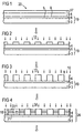
- an electrically conductive semiconductor layer 6 (for example a buffer layer) is applied to a main surface 5 of a growth substrate wafer 3 preferably made of SiC, for example by means of MOVPE (metal organic vapor phase epitaxy).
- B. consists of GaN and / or AlGaN.
- a mask layer 4, for example consisting of SiO 2 or Si x N 1-x is subsequently applied to this substrate wafer 19 consisting of the growth substrate 3 and the semiconductor layer 6, on which in turn a photoresist layer 17 is deposited.
- the wafer 20 produced in this way is shown schematically in FIG. 1.
- the photoresist layer 17 becomes the mask layer 4, for example in a manner known per se by means of a isotropic wet chemical (e.g. photo-etching solution) or by means of a dry chemical etching process 12 ( Figure 2), the is preferably selective for the material of the semiconductor layer 6, with a plurality of mask openings 10 (windows) provided such that in the mask openings 10 from the Growth substrate 3 facing away from the main surface 9 of the Semiconductor layer 6 is exposed ( Figure 3).
- a isotropic wet chemical e.g. photo-etching solution
- a dry chemical etching process 12 Figure 2
- a Ga (In, Al) N semiconductor layer sequence 18 (FIG. 4), consisting of a plurality of, is applied, for example, by means of organometallic vapor phase epitaxy (MOVPE) 13 (FIG. 3) onto the main surface 9 of the semiconductor layer 6 exposed in the windows 10 Ga (In, Al) N layers selectively epitaxially deposited.
- MOVPE organometallic vapor phase epitaxy
- semiconductor material of the light-emitting diode structure is deposited epitaxially, ie monocrystalline, only on the main surface 9 of the semiconductor layer 6 and not on the mask layer 4. Only a polycrystalline growth takes place on the mask layer 4, if at all.
- the Ga (In, Al) N semiconductor layer sequence 18 has, for example, a light-emitting active layer 23 arranged between an n-doped 21 and a p-doped Ga y Al 1-y N (0 ⁇ y ⁇ 1) cladding layer 22 consists of n-doped In x Ga 1-x N (0 ⁇ x ⁇ 1).
- compositions, layer thicknesses, doping etc. of the individual layers of Ga (In, Al) N semiconductor layer sequences 18 for light-emitting diode chips 100 are known in semiconductor technology and are therefore not explained in more detail here. The same applies to the etching processes for the isotropic and anisotropic etching of Sio 2 and Si x N 1-x .
- the one facing away from the light emitting diode structures 2 Side of the substrate wafer 3 before or after processing the Light-emitting diode structures 2 with a rear-side contact metallization layer 16 provided.
- the mask layer 4 Semiconductor layer 6 applied to the growth substrate 3 become. Rather, the mask layer 4 can directly on the Main surface 5 of the growth substrate 3, which then alone Forms substrate wafer 19 to be deposited.
- the selective Epitaxy of the light emitting diode structures 2 if necessary including the buffer layer is then made after the Window 10 in the mask layer 4 also on the Main surface 5 of the growth substrate 3.
- VCSEL Very Cavity Surface Emitting laser
- a mask layer 4 is applied over the entire surface of a main surface 9 of a substrate wafer 19, on which a semiconductor layer 6 can already be applied (indicated by dashed lines in the figures).
- the growth substrate 3 consists for example of SiC or sapphire and the mask layer 4 of SiO 2 or Si x N 1-x .
- the semiconductor layer 6 is, for example, an Al x Ga 1-x N epitaxial layer (0 x x 1 1) and serves z. B. as a buffer layer.
- a plurality of windows 10 (for example a round, rectangular or square recess or trench) in which the main surface 9 of the substrate wafer 19 is exposed are subsequently formed, for example by means of wet or dry etching, in the mask layer 4.
- Etching agents for etching SiO 2 or Si x N 1-x are known in semiconductor technology and are therefore not explained in more detail here.
- the exposed main area 9 of the substrate wafer 19 by means of selective epitaxy Semiconductor layer sequence 2 of an edge emitting Laser structure based on Ga (In, Al) N applied.
- the Windows 10 each have two opposite one another plane-parallel surface areas 7, the two laser mirror surfaces 8 lying plane-parallel to one another Define edge emitting laser structures 2.
- Selective epitaxy means that the semiconductor material of the Semiconductor layer sequence only on the substrate surface and not epitaxially on the mask layer, i.e. single crystal is deposited.
- the window 10 is closed by means of a first Substrate wafer 19 selective etching step and the Mask layer 4 is covered by means of a second Semiconductor layer sequence 2 selective etching step removed.
- the mask layer 4 is, for example, by means of wet or dry chemical etching of the substrate wafer 19 removed, so that the semiconductor layer sequence 2 as a laser semiconductor body remains free-standing on the substrate 3.
- the wafer produced in this way then becomes edge-emitting Laser chips 200 isolated.
Abstract
Description
Die Erfindung bezieht sich auf ein Verfahren zum Herstellen
einer Mehrzahl von Halbleiterkörpern, insbesondere von
strahlungsemittierenden Halbleiterköpern, gemäß dem
Oberbegriff des Patentanspruches 1.The invention relates to a method for manufacturing
a plurality of semiconductor bodies, in particular of
radiation-emitting semiconductor bodies, according to the
Preamble of
Sie bezieht sich insbesondere
- auf ein Verfahren zum Herstellen einer Mehrzahl von Leuchtdiodenchips, bei dem auf einer Hauptfläche eines Substratwafers eine Mehrzahl von Halbleiterschichten abgeschieden werden, von denen mindestens eine ein III-V-Verbindungshalbleitermaterial aufweist, das auf GaN-basiert, wie zum Beispiel GaN, GaAlN, InGaN oder InAlGaN, und
- auf ein Verfahren zum Herstellen einer Mehrzahl von kantenemittierenden Halbleiterlaserchips, die an mindestens zwei einander gegenüberliegenden Seitenflächen planparallel zueinander liegende Laserspiegelflächen aufweisen.
- to a method for producing a plurality of light-emitting diode chips, in which a plurality of semiconductor layers are deposited on a main surface of a substrate wafer, at least one of which has a III-V compound semiconductor material based on GaN, such as, for example, GaN, GaAlN, InGaN or InAlGaN, and
- to a method for producing a plurality of edge-emitting semiconductor laser chips which have laser mirror surfaces lying plane-parallel to one another on at least two opposite side surfaces.
Derartige Verfahren sind bekannt. Zur Herstellung von Lumineszenzdiodenchips wird zum Beispiel auf einem Halbleitersubstratwafer eine elektrolumineszierende Halbleiterschichtenfolge epitaktisch aufgewachsen. Dieser sogenannte Epi-Wafer wird nachfolgend, nachdem er mit den erforderlichen Kontaktmetallisierungen zur elektrischen Kontaktierung der Lumineszenzdiodenchips versehen ist, mittels Sägen zu Lumineszenzdiodenchips zerteilt. Ähnliche Verfahren werden bei Transistor-, IC-Chips usw. verwendet.Such methods are known. For production of Luminescent diode chips are, for example, on a Semiconductor substrate wafer an electroluminescent Semiconductor layer sequence grew epitaxially. This so-called epi-wafer is subsequently after it with the required contact metallizations for electrical Contacting of the luminescence diode chips is provided, cut into luminescent diode chips by sawing. Similar Methods are used with transistor, IC chips, etc.
In der EP 0 599 224 A1 ist ein Verfahren beschrieben, bei dem eine Mehrzahl von InxGa1-xN-Schichten auf einem Substrat epitaktisch abgeschieden werden. Diese Mehrzahl von InxGa1-xN-Schichten bilden eine Leuchtdioden(LED) -Schichten-folge, die sich über den gesamten Wafer erstreckt. Nach dem Abscheiden der LED-Schichtenfolge, deren Strukturierung mittels Ätzen und dem Aufbringen einer Mehrzahl von Kontaktmetallisierungen wird der Wafer in eine Vielzahl von einzelnen Leuchtdiodenchips vereinzelt, indem der Wafer zwischen den Kontaktmetallisierungen beispielsweise mittels Sägen durchtrennt wird.EP 0 599 224 A1 describes a method in which a plurality of In x Ga 1-x N layers are epitaxially deposited on a substrate. This plurality of In x Ga 1-x N layers form a light-emitting diode (LED) layer sequence which extends over the entire wafer. After the deposition of the LED layer sequence, its structuring by means of etching and the application of a plurality of contact metallizations, the wafer is separated into a plurality of individual light-emitting diode chips by severing the wafer between the contact metallizations, for example by means of saws.
Bei der Abscheidung von Ga(In,Al)N-Leuchtdiodenstrukturen
besteht unabhängig vom Substratmaterial das besondere Problem
stark abweichender Gitterkonstanten der Nitride zu den
entsprechenden Substraten. Eine weitere Schwierigkeit stellen
die stark unterschiedlichen thermischen
Ausdehnungskoeffizienten der zur Verfügung stehenden
Substratmaterialien (z. B. Saphir oder SiC) und des Systems
Ga(In,Al)N dar. Die dadurch hervorgerufenen unterschiedlichen
thermischen Ausdehnungen bewirken, daß beim Abkühlen des
Wafers von der Wachstumstemperatur auf Raumtemperatur im
Wafer thermisch induzierte Verspannungen auftreten. Dies
führt zu Defekten in den Halbleiterstrukturen, in erster
Linie ![]()
![]()
Ein weiteres Problem, das bei Ga(In,Al)N-Leuchtdiodenstrukturen auftritt, besteht darin, daß dieses Materialsystem chemisch sehr stabil ist. Diese Eigenschaft wirft große Probleme bei der Bauelementstrukturierung auf. Strukturierungen der Ga(In,Al)N-Schichtenfolgen auf dem Wafer sind nur mittels technisch aufwendiger Methoden, wie Trockenätzverfahren oder UV-unterstützte naßchemische Ätzverfahren, möglich.Another problem with Ga (In, Al) N light emitting diode structures occurs, is that this material system is chemically very stable. This property throws great Problems with component structuring. Structuring of the Ga (In, Al) N layer sequences on the wafer are only by means of technically complex methods such as Dry etching or UV-assisted wet chemical Etching process, possible.
Außerdem können beispielsweise Saphir und GaN wegen ihrer großen Härte nur mit großem technischen Aufwand gesägt werden. In addition, for example, sapphire and GaN can be used because of their sawed hardness only with great technical effort become.
Bei einem bekannten Verfahren zur Herstellung von kantenemittierenden Laserdioden wird zur Realisierung der Laserspiegel beispielsweise ein die Laserdiodenstrukturen aufweisender Epi-Halbleiterwafer entsprechend den kristallographichen Richtungen des Substrats gespalten.In a known method for producing edge emitting laser diodes is used to implement the Laser mirror, for example, the laser diode structures having epi semiconductor wafer according to the cleaved crystallographic directions of the substrate.
Die Herstellung von aus Halbleitermaterialien unterschiedlichster Art bestehenden Halbleiterkörpern auf verschiedensten Substratkristallen erlaubt immer weniger die Nutzung kristallographischer Richtungen des Substrates zur Herstellung von Laserspiegeln durch einfaches Spalten. Aufwendige Techniken, wie Naß- oder Trockenätzverfahren werden daher notwendig, um Laserspiegel exakt planparallel und mit geringer Rauhigkeit zu realisieren. Verschiedene Halbleitermaterialsysteme, wie beispielsweise Ga(In,Al)N haben sogar die Eigenschaft, gegen übliche naßchemische Ätzen resistent zu sein. In diesen Fällen ist man völlig auf technisch aufwendige und damit teure Trockenätzverfahren angewiesen.The manufacture of semiconductor materials different types of existing semiconductor bodies The most varied substrate crystals allow less and less Use of crystallographic directions of the substrate Manufacture of laser mirrors by simple splitting. Elaborate techniques such as wet or dry etching are therefore necessary to make laser mirrors exactly plane-parallel and to be realized with low roughness. Various Semiconductor material systems, such as Ga (In, Al) N even have the property against conventional wet chemical etching to be resistant. In these cases you are completely up technically complex and therefore expensive dry etching processes reliant.
Die Aufgabe der vorliegenden Erfindung besteht darin, ein Verfahren der eingangs genannten Art anzugeben, das es ermöglicht, auch bei der Verwendung von mechanisch und chemisch sehr stabilen Halbleitermaterialien und/oder von Substrat- und Epitaxieschichtmaterialien mit stark voneinander abweichenden Gitterkonstanten auf einfache Weise eine Mehrzahl von Halbleiterkörpern mit genau definierten Seitenflächen und/oder reduzierten Kristallstörungen herzustellen.The object of the present invention is a Procedure of the type mentioned to indicate that it allows, even when using mechanical and chemically very stable semiconductor materials and / or of Substrate and epitaxial layer materials with strong different lattice constants in a simple way a plurality of semiconductor bodies with precisely defined Side faces and / or reduced crystal disturbances to manufacture.
Es soll insbesondere ein Verfahren zur Herstellung von Ga(In,Al)N-Leuchtdiodenchips angegeben werden, mit dem Kristallstörungen in den Halbleiterstrukturen verringert werden und bei dem technisch einfache Methoden zur Strukturierung von Ga(In,Al)N-Schichtenfolgen eingesetzt werden können. In particular, it is intended to be a method for producing Ga (In, Al) N LED chips can be specified with the Crystal disturbances in the semiconductor structures reduced become and where technically simple methods for Structuring of Ga (In, Al) N layer sequences used can be.
Weiterhin soll insbesondere ein einfaches Verfahren zum Herstellen von Laserspiegeln eines kantenemittierenden Laser-Halbleiterkörpers, insbesondere bestehend aus verschiedenen Halbleiterschichten aus dem Materialsystem Ga(In,Al)N, angegeben werden.Furthermore, a simple method for Manufacture of laser mirrors of an edge-emitting laser semiconductor body, in particular consisting of various Semiconductor layers from the material system Ga (In, Al) N, can be specified.
Diese Aufgabe wird durch ein Verfahren mit den Merkmalen des
Anspruches 1 gelöst. Vorteilhafte Weiterbildungen des
Verfahrens, insbesondere besonders bevorzugte Verfahren zum
Herstellen von Ga(In,Al)N-Leuchtdiodenchips und zum
Herstellen von kantenemittierende Ga(In,Al)N-Halbleiterlaserchips
sind Gegenstand der Unteransprüche 2 bis
13.This task is accomplished by a process with the characteristics of
Bei dem Verfahren wird vorzugsweise zunächst auf den Substratwafer eine gut ätzbare Maskenschicht aufgebracht, die nachfolgend beispielsweise mittels Phototechnik mit einer Mehrzahl von Maskenöffnungen (Fenstern) versehen wird, in denen die Hauptfläche des Substratwafers freigelegt ist. Nachfolgend wird die Halbleiterschichtenfolge von Leuchtdiodenstrukturen oder von Halbleiterlaserstrukturen in den Fenstern auf der Hauptfläche des Substratwafers abgeschieden. Die Fenster definieren hierbei die laterale Form der Halbleiterschichtenfolge. Nach einem Aufbringen von Kontaktmetallisierungen auf den derart hergestellten Wafer wird dieser in einzelne Leuchtdiodenchips oder Halbleiterlaserchips vereinzelt.In the method, the first step is preferably to Applied a highly etchable mask layer, the substrate wafer subsequently, for example, using a photo technology A plurality of mask openings (windows) is provided in which the main surface of the substrate wafer is exposed. The semiconductor layer sequence of Light emitting diode structures or semiconductor laser structures in the windows on the main surface of the substrate wafer deposited. The windows define the lateral Shape of the semiconductor layer sequence. After applying Contact metallizations on the wafer produced in this way is this in individual LED chips or Semiconductor laser chips isolated.
Als Maskenschicht dient vorteilhafterweise eine dielektrische Schicht aus SiO2 oder SixN1-x und die Fenster werden beispielsweise mittels eines isotropen naßchemischen Ätzverfahrens (z. B. mit herkömmlicher Fensterätzlösung) oder mittels eines trockenchemischen Ätzverfahrens hergestellt, das vorzugsweise gegenüber dem Substratmaterial selektiv ist.A dielectric layer made of SiO 2 or Si x N 1-x is advantageously used as the mask layer and the windows are produced, for example, by means of an isotropic wet chemical etching process (e.g. using a conventional window etching solution) or by means of a dry chemical etching process, which is preferably selective with respect to the substrate material .
Besonders bevorzugt wird das Verfahren bei Halbleiterkörpern eingesetzt, bei denen das Substrat aus SiC, Saphir oder GaN besteht und bei denen die Halbleiterschichtenfolge mindestens eine Halbleiterschicht aus dem Materialsystem Ga(In,Al)N aufweist.The method is particularly preferred for semiconductor bodies used in which the substrate made of SiC, sapphire or GaN exists and in which the semiconductor layer sequence at least a semiconductor layer made of the Ga (In, Al) N material system having.
Insbesondere sind dies Leuchtdiodenstrukturen oder Halbleiterlaserstrukturen [z.B. kantenemittierende Laserdioden und VCSEL(Vertical Cavity Surface Emitting Laser)-Dioden], die mindestens eine Halbleiterschicht aus dem Materialsystem der auf GaN-basierenden III-V-Verbindungshalbleiter, wie z.B. Ga1-x-yInxAlyN mit 0≤x<1, 0≤y<1 und x+y<1, aufweisen, weil hier die eingangs erwähnten Probleme in besonderem Maße zur Geltung kommen.In particular, these are light-emitting diode structures or semiconductor laser structures [for example edge-emitting laser diodes and VCSEL (Vertical Cavity Surface Emitting Laser) diodes], which contain at least one semiconductor layer from the material system of the GaN-based III-V compound semiconductors, such as Ga 1-xy In x Al y N with 0≤x <1, 0≤y <1 and x + y <1, because the problems mentioned at the outset are particularly important here.
Dies sind beispielsweise blaues oder grünes Licht aussendende Laserdioden, bei denen als Halbleiterschichtenfolge eine kantenemittierende Laser-Halbleiterstruktur vorgesehen ist, die an zwei einander gegenüberliegenden Seitenflächen planparallel zueinander liegende Laserspiegelflächen aufweist. Die Laserspiegel werden bei dem erfindungsgemäßen Verfahren durch zwei einander exakt planparallel gegenüberliegende Seitenflächen der Maskenöffnungen definiert.These are, for example, blue or green light emitting Laser diodes in which a semiconductor layer sequence edge-emitting laser semiconductor structure is provided, the two on opposite sides plane-parallel laser mirror surfaces having. The laser mirrors are used in the invention Process by two exactly plane-parallel to each other opposite side faces of the mask openings Are defined.
Bei der Herstellung von kantenemittierenden Halbleiterlaserchips wird vorzugsweise die Maskenschicht wieder entfernt, bevorzugt durch selektives Ätzen (selektiv zur Halbleiterschichtenfolge).In the manufacture of edge emitting Semiconductor laser chips are preferably the mask layer removed again, preferably by selective etching (selective to the semiconductor layer sequence).
Zur Vereinzelung des so erzeugten Wafers in einzelne Chips wird nur noch die Maskenschicht (falls diese nicht vorher entfernt wurde), der Substratwafer und ggf. eine auf der Rückseite (= die von den Leuchtdiodenstrukturen abgewandte Hauptfläche des Substratwafers) aufgebrachte Kontaktmetallisierung zwischen den Leuchtdiodenstrukturen durchtrennt werden. Damit kommt es bei diesem Verfahren vorteilhafterweise zu keiner Beschädigung der Halbleiterschichtenfolgen beim Sägen und/oder Brechen des Wafers.For separating the wafer produced in this way into individual chips only the mask layer (if not before was removed), the substrate wafer and possibly one on the Rear side (= the one facing away from the light emitting diode structures Main surface of the substrate wafer) applied Contact metallization between the light emitting diode structures be severed. This is what happens with this procedure advantageously no damage to the Semiconductor layer sequences when sawing and / or breaking the Wafers.
Auch beim Herstellen von Leuchtdiodenchips kann es vorteilhaft sein, daß vor dem Vereinzeln des Wafers in Leuchtdiodenchips die zwischen den Leuchtdiodenstrukturen befindliche Maskenschicht entfernt wird, so daß einzelne, voneinander getrennte Leuchtdiodenstrukturen auf dem Substrat zurückbleiben. Nachfolgend muß dann nur noch der Substratwafer und ggf. eine Kontaktmetallisierung auf dessen Rückseite zwischen den Leuchtdiodenstrukturen durchtrennt werden.It can also be used when manufacturing LED chips be advantageous in that before the wafer is separated Light emitting diode chips between the light emitting diode structures located mask layer is removed so that individual, separate LED structures on the substrate stay behind. Then only the Substrate wafer and possibly a contact metallization on it Cut through the back between the light emitting diode structures become.
Diese optionale Entfernen der Maskenschicht nach dem Abscheiden von Leuchtdiodenstrukturen erfolgt beispielsweise mittels eines naßchemischen Ätzverfahrens, bei dem die Leuchtdiodenstrukturen überhaupt nicht oder nur in sehr geringem Umfang abgetragen werden.This optional removal of the mask layer after the Deposition of light emitting diode structures takes place, for example by means of a wet chemical etching process in which the Light emitting diode structures not at all or only in a very large number to a small extent.
Ein Vorteil des Verfahrens besteht einerseits darin, daß die Form und Dimension der späteren Leuchtdioden-Chips oder Halbleiterlaserchips vor der Epitaxie der Halbleiterschichtenfolge dieser Chips definiert werden, wodurch gegenüber den bekannten Verfahren mehrere Prozeßschritte eingespart werden können.One advantage of the method is that the Shape and dimension of the later LED chips or Semiconductor laser chips before the epitaxy of Semiconductor layer sequence of these chips are defined whereby several compared to the known methods Process steps can be saved.
Andererseits ermöglicht dieses Verfahren vorteilhafterweise die Abscheidung stark verspannter Strukturen in den vordefinierten Fenstern. Der abgeschiedene Kristall besitzt hierbei die Möglichkeit, sich in drei Raumrichtungen auszudehnen und somit die potentielle Verspannungsenergie im Volumen abzubauen, ohne entsprechende Versetzungen ausbilden zu müssen.On the other hand, this method advantageously enables the deposition of highly strained structures in the predefined windows. The deposited crystal has here the possibility of moving in three spatial directions expand and thus the potential tension energy in the Reduce volume without forming appropriate dislocations to have to.
Weiterhin werden vorteilhafterweise weniger Defekte in den Kristall eingebaut, da bereits während des Wachstums Verspannungen in den kristallinen Schichten abgebaut werden können.Furthermore, fewer defects are advantageously in the Crystal built in as it grows Tensions in the crystalline layers are reduced can.
Im Fall der weiter oben beschriebenen bekannten planaren Epitaxie (ohne Maske) werden im Kristall zum Abbau der potentiellen Verspannungsenergie Defekte erzeugt. Diese Defekte beeinträchtigen nachhaltig das spätere Bauelement in der Art, daß beispielsweise die Lebensdauer verkürzt und/oder die ESD-Stabilität deutlich reduziert ist. Eine Reduzierung der Defekte mittels des erfindungsgemäßen Verfahrens äußert sich demzufolge direkt in einer Verbesserung dieser Bauelementeigenschaften.In the case of the known planar described above Epitaxy (without a mask) are used in the crystal to break down the potential tension energy defects. This Defects have a lasting effect on the later component the way that, for example, shortens the lifespan and / or ESD stability is significantly reduced. A reduction the defects expresses by means of the method according to the invention consequently directly in an improvement of this Component properties.
Ein wesentliches Merkmal des vorliegenden Verfahrens besteht in der selektiven Abscheidung der Leuchtdiodenstrukturen oder Halbleiterlaserstrukturen in den Maskenöffnungen (Fenstern). Die Maskenschicht sowie die Abscheidebedingungen können derart gewählt werden, daß auf der Maske eine epitaktische, d. h. einkristalline Abscheidung von Ga(In,Al)N-Material nicht erfolgt.There is an essential feature of the present method in the selective deposition of the light emitting diode structures or Semiconductor laser structures in the mask openings (windows). The mask layer and the deposition conditions can be chosen such that an epitaxial, d. H. single-crystal deposition of Ga (In, Al) N material not happened.
Anwendbar ist dieses Verfahren sowohl auf Saphir als auch auf SiC, Si, GaAs, GaN, AlN etc. als Aufwachs-Substratmaterial. Viele Schwierigkeiten, die beim Brechen bzw. Ätzen von mittels planarer Epitaxie hergestellten Scheiben, insbesondere von Ga(in,Al)N-Epitaxiewafern zur Herstellung von Leuchtdioden- oder Halbleiterlaserchips verschiedenster Art auftreten, werden mit diesem Verfahren umgangen.This process is applicable to both sapphire and SiC, Si, GaAs, GaN, AlN etc. as growth substrate material. Many difficulties in breaking or etching disks made by planar epitaxy, in particular of Ga (in, Al) N epitaxial wafers for production of light emitting diodes or semiconductor laser chips Kind occur, are avoided with this procedure.
Bei einer bevorzugten Ausführungsform des Verfahrens wird vor dem Aufbringen der Maskenschicht auf einem Aufwachs-Substratwafer eine Pufferschicht, z. B. bestehend aus Ga(In,Al)N, aufgewachsen. Auf dieser werden dann in nachfolgenden Prozessschritten die Maskenschicht und die Halbleiterschichtenfolgen für die Leuchtdiodenstrukturen oder Halbleiterlaserstrukturen abgeschieden. Dies kann vorteilhafterweise die Aufwachsbedingungen für die Halbleiterschichtenfolgen verbessern.In a preferred embodiment of the method is before the application of the mask layer on a growth substrate wafer a buffer layer, e.g. B. consisting of Ga (In, Al) N, grew up. On this are then in subsequent process steps the mask layer and the Semiconductor layer sequences for the light emitting diode structures or Semiconductor laser structures deposited. This can advantageously the growing conditions for the Improve semiconductor layer sequences.
Ein wesentlicher Vorteil des erfindungsgemäßen Verfahrens bei der Herstellung von kantenemittierenden Halbleiterlaserchips besteht darin, dass die Definitionder Laserspiegel bereits vor der epitaktischen Abscheidung der Halbleiterschichtfolge stattfindet. Die Maskenschicht weist hierbei vorzugsweise mindestens eine Dicke auf, die dem lichtführenden Bereich des vorgesehenen Laser-Halbleiterkörpers entspricht und vertikal im Bereich der Lichtentstehung im vorgesehenen Laser-Halbleiterkörper angesiedelt ist. Mit Hilfe von naß- oder trockenchemischen Ätzverfahren werden die Laserspiegel und, soweit möglich, alle anderen notwendigen Begrenzungen der Halbleiterschichtenfolge in diese Schicht geätzt, wobei auf möglichst scharfe Ätzkanten und glatte Ätzflanken zu achten ist. Die spätere laterale Form der Halbleiterschichtenfolge des Halbleiterlaserchips wird bereits bei diesem Prozeß in ihren geometrischen Verhältnissen definiert.A major advantage of the method according to the invention the production of edge-emitting semiconductor laser chips is that the definition of the laser mirror already before the epitaxial deposition of the semiconductor layer sequence takes place. The mask layer preferably has at least a thickness that corresponds to the light-guiding region of the provided laser semiconductor body corresponds and vertically in the area of light generation in the intended laser semiconductor body is located. With the help of wet or dry chemical etching processes, the laser mirrors and, as far as possible, all other necessary limitations of the Semiconductor layer sequence etched into this layer, being on as sharp as possible etching edges and smooth etching flanks is. The later lateral form of the semiconductor layer sequence the semiconductor laser chip is already in this process defined their geometric relationships.
In den entstehenden Ätzfenstern wird das Substratmaterial freigelegt, das einer anschließenden Epitaxie als Substratfläche dient. Durch selektive Epitaxie, bei der die Halbleitermaterialien der Halbleiterschichtfolge nur auf der Oberfläche des Substratwafers in den Fenstern abgeschieden werden, wird dann die Laserstruktur, insbesondere der lichtführende sowie der aktive Bereich des Laser-Halbleiterkörpers hergestellt.The substrate material is in the resulting etching window exposed to subsequent epitaxy as Serves substrate surface. Through selective epitaxy, in which the Semiconductor materials of the semiconductor layer sequence only on the Surface of the substrate wafer deposited in the windows then the laser structure, especially the light-guiding as well as the active area of the laser semiconductor body manufactured.
Nach Abschluß der Epitaxie wird die gut ätzbare Schicht durch Ätzen mit geeigneten Chemikalien naß- oder trockenchemisch entfernt. Die dadurch erzeugte Struktur besitzt nun bereits die geometrischen Umrisse des Laser-Halbleiterkörpers mit sehr gut definierten Laserspiegeln. After the epitaxy is complete, the easily etchable layer is through Etch with suitable chemicals, wet or dry chemical away. The structure created by this now already has with the geometric outline of the laser semiconductor body very well defined laser mirrors.
Das Verfahren wird im folgenden anhand von drei
Ausführungsbeispielen in Verbindung mit den Figuren 1 bis 10
näher erläutert.
In den Figuren sind gleiche oder gleichwirkende Bestandteile jeweils mit denselben Bezugszeichen versehen.In the figures, the same or equivalent components each provided with the same reference numerals.
Zunächst wird auf eine Hauptfläche 5 eines bevorzugt aus SiC
bestehenden Aufwachs-Substratwafers 3 beispielsweise mittels
MOVPE (Metallorganische Dampfphasenepitaxie) eine elektrisch
leitfähige Halbleiterschicht 6 (z.B. eine Bufferschicht)
aufgebracht, die z. B. aus GaN und/oder AlGaN besteht. Auf
diesen aus dem Aufwachs-Substrat 3 und der Halbleiterschicht
6 bestehenden Substratwafer 19 wird nachfolgend eine
Maskenschicht 4, beispielsweise bestehend aus SiO2 oder SixN1-x,
aufgebracht, auf der wiederum eine Photolackschicht 17
abgeschieden wird. Der auf diese Weise hergestellte Wafer 20
ist in Figur 1 schematisch dargestellt.First, an electrically conductive semiconductor layer 6 (for example a buffer layer) is applied to a
Nach einer herkömmlichen phototechnischen Strukturierung der
Photolackschicht 17 wird die Maskenschicht 4 beispielsweise
auf eine an sich bekannte Art und Weise mittels eines
isotropennaßchemischen (z. B. Photo-Ätzlösung) oder mittels
eines trockenchemischen Ätzverfahrens 12 (Figur 2), das
bevorzugt zum Material der Halbleiterschicht 6 selektiv ist,
mit einer Mehrzahl von Maskenöffnungen 10 (Fenstern)
versehen, derart, daß in den Maskenöffnungen 10 die vom
Aufwachs-Substrat 3 abgewandte Hauptfläche 9 der
Halbleiterschicht 6 freigelegt ist (Figur 3).After a conventional phototechnical structuring of the
Bei einem nachfolgenden Verfahrensschritt wird beispielsweise
mittels metallorganischer Dampfphasenepitaxie (MOVPE) 13
(Figur 3) auf die in den Fenstern 10 freigelegte Hauptfläche
9 der Halbleiterschicht 6 eine Ga(In,Al)N-Halbleiterschichtenfolge
18 (Figur 4), bestehend aus einer
Mehrzahl von Ga(In,Al)N-Schichten selektiv epitaktisch
abgeschieden. Unter
Die Ga(In,Al)N-Halbleiterschichtenfolge 18 weist
beispielsweise eine zwischen einer n-dotierten 21 und einer
p-dotierten GayAl1-yN(0≤y≤1)-Mantelschicht 22 angeordnete
lichtemittierende aktive Schicht 23 auf, die aus n-dotiertem
InxGa1-xN (0<x<1) besteht.The Ga (In, Al) N
Die Zusammensetzungen, Schichtdicken, Dotierungen etc. der
einzelnen Schichten von Ga(In,Al)N-Halbleiterschichtenfolgen
18 für Leuchtdiodenchips 100 sind in der Halbleitertechnik
bekannt und werden daher an dieser Stelle nicht näher
erläutert. Gleiches gilt für die Ätzverfahren zum isotropen
und anisotropen Ätzen von Sio2 und SixN1-x.The compositions, layer thicknesses, doping etc. of the individual layers of Ga (In, Al) N
Nach der selektiven Epitaxie der Ga(In,Al)N-Halbleiterschichtenfolge
18 wird, wie in Figur 4 dargestellt, die
Maskenschicht 4 mittels einer zur Ga(In,Al)N-Halbleiterschich-tenfolge
18 selektiven naßchemischen oder
trockenchemischen Ätzung 14 von dem vorliegenden Wafer 24
(genauer, von der Hauptfläche 9 der Halbleiterschicht 6)
entfernt, so daß freistehende Leuchtdiodenstrukturen 2 auf
dem Substratwafer 19 zurückbleiben (Figur 5).After the selective epitaxy of the Ga (In, Al) N
Zur Kontaktierung der Leuchtdiodenstrukturen 2 müssen, wie in
Figur 5 gezeigt, auf diese noch Vorderseiten-Kontaktmetallisierungen
15 aufgebracht werden. Dieser Schritt erfolgt
vorteilhafterweise vor dem Entfernen der Maskenschicht 4 z.
B. mittels Phototechnik und Metallisierung. Hierzu kann
wiederum ein in der Halbleitertechnik herkömmliches
Metallisierungsverfahren eingesetzt werden.To contact the light emitting diode structures 2, as in
Figure 5 shown, on these front-
Ebenso wird die von den Leuchtdiodenstrukturen 2 abgewandte
Seite des Substratwafers 3 vor oder nach dem Prozessieren der
Leuchtdiodenstrukturen 2 mit einer Rückseiten-Kontaktmetallisierungsschicht
16 versehen.Likewise, the one facing away from the light emitting diode structures 2
Side of the
Danach wird der Substratwafer 19 mit Rückseiten-Kontaktmetallisierungsschicht
16 zwischen den
Leuchtdiodenstrukturen 2 durchtrennt, so daß einzelne
Leuchtdiodenchips 100 entstehen (Figur 6).Thereafter, the
Bei dem Verfahren gemäß der Erfindung muß nicht
notwendigerweise vor dem Aufbringen der Maskenschicht 4 eine
Halbleiterschicht 6 auf das Aufwachs-Substrat 3 aufgebracht
werden. Vielmehr kann die Maskenschicht 4 direkt auf die
Hauptfläche 5 des Aufwachs-Substrats 3, das dann alleine den
Substratwafer 19 bildet, abgeschieden werden. Die selektive
Epitaxie der Leuchtdiodenstrukturen 2 gegebenenfalls
inclusive Bufferschicht erfolgt dann nach dem Herstellen der
Fenster 10 in der Maskenschicht 4 ebenfalls auf der
Hauptfläche 5 des Aufwachs-Substrats 3.In the method according to the invention does not have to
necessarily one before applying the
Auf ähnliche Weise können VCSEL(Vertical Cavity Surface Emitting Laser)-Chips hergestellt werden. Similarly, VCSEL (Vertical Cavity Surface Emitting laser) chips are manufactured.
Hier wird die Maskenschicht 4 vor dem Vereinzeln des Wafers
24 zu einzelnen Leuchtdiodenchips 100 nicht entfernt, so daß
die Leuchtdiodenchips 100, wie in Figur 7 dargestellt, neben
der Leuchtdiodenstruktur 2 nach dem Vereinzeln des Wafers mit
der Maskenschicht 4 versehen sind. Dadurch kann
vorteilhafterweise ein Ätzschritt eingespart werden.Here is the
Zunächst wird auf eine Hauptfläche 9 eines Substratwafers 19,
auf dem bereits eine Halbleiterschicht 6 aufgebracht sein
kann (in den Figuren gestrichelt angedeutet), ganzflächig
eine Maskenschicht 4 aufgebracht. Das Aufwachs-Substrat 3
besteht beispielsweise aus SiC oder Saphir und die
Maskenschicht 4 aus SiO2 oder SixN1-x. Die Halbleiterschicht 6
ist ggf. beispielsweise eine AlxGa1-xN-Epitaxieschicht (0 ≤ x
≤ 1) und dient z. B. als Bufferschicht.First, a
Nachfolgend werden beispielsweise mittels Naß- oder
Trockenätzen in der Maskenschicht 4 eine Mehrzahl von Fenster
10 (z.B. eine runde, rechteckige oder quadratische Ausnehmung
oder Graben) augebildet, in denen die Hauptfläche 9 des
Substratwafers 19 freigelegt ist. Ätzmittel zum Ätzen von
SiO2 oder SixN1-x sind ind er Halbleitertechnik bekannt und
werden von daher an dieser Stelle nicht näher erläutert.A plurality of windows 10 (for example a round, rectangular or square recess or trench) in which the
Beim nächsten Schritt wird auf die freigelegte Hauptfläche 9
des Substratwafers 19 mittels selektiver Epitaxie eine
Halbleiterschichtenfolge 2 einer kantenemittierenden
Laserstruktur auf der Basis von Ga(In,Al)N aufgebracht. Die
Fenster 10 weisen jeweils zwei einander gegenüberliegende
planparallele Seintenflächen 7 auf, die die beiden
planparallel zueinander liegenden Laserspiegelflächen 8 der
kantenemittierenden Laserstrukturen 2 definieren.In the next step, the exposed
Selektive Epitaxie bedeutet, daß das Halbleitermaterial der Halbleiterschichtenfolge nur auf der Substratoberfläche und nicht auf der Maskenschicht epitaktisch, d.h. einkristallin abgeschieden wird.Selective epitaxy means that the semiconductor material of the Semiconductor layer sequence only on the substrate surface and not epitaxially on the mask layer, i.e. single crystal is deposited.
Das Fenster 10 wird mittels eines ersten bzgl. des
Substratwafers 19 selektiven Ätzschrittes ausgebildet und die
Maskenschicht 4 wird mittels eines zweiten bzgl. der
Halbleiterschichtenfolge 2 selektiven Ätzschrittes entfernt.The
Abschließend wird die Maskenschicht 4 beispielsweise mittels
naß- oder trockenchemischer Ätzung vom Substratwafer 19
entfernt, so daß die Halbleiterschichtenfolge 2 als Laser-Halbleiterkörper
freistehend auf dem Substrat 3 verbleibt.
Der so erzeugte Wafer wird dann zu kantenemittierenden
Laserchips 200 vereinzelt.Finally, the
Die Beschreibung des erfindungsgemäßen Verfahrens anhand dieser Ausführungsbeispiele ist selbstverständlich nicht als Beschränkung der Erfindung auf diese Beispiele zu verstehen. Der Fachmann kann das Verfahren überall dort einsetzen, wo die eingangs geschilderten Probleme auftreten.The description of the method according to the invention based on of these embodiments is of course not as Limitation of the invention to understand these examples. The person skilled in the art can use the method wherever the problems described at the beginning occur.
Claims (14)
bei dem auf einer Hauptfläche (9) eines Substratwafers (19) eine Halbleiterschichtenfolge (18) abgeschieden wird,
dadurch gekennzeichnet, daß
in which a semiconductor layer sequence (18) is deposited on a main surface (9) of a substrate wafer (19),
characterized in that
dadurch gekennzeichnet, dass eine Mehrzahl von Ga(In,Al)N-Leuchtdiodenchips (100) hergesellt wird, wobei eine Ga(In,Al)N-Halbleiterschichtenfolge (18) auf die in den Fenstern (10) freigelegte Hauptfläche (9) des Substratwafers (19) abgeschieden wird, so daß in den Fenstern (10) Ga(In,Al)N-Leuchtdiodenstrukturen (2) entstehen, und der so hergestellte Wafer (24) mittels Durchtrennen zwischen den Ga(In,Al)N-Leuchtdiodenstrukturen (2) zu Ga(In,Al)N-Leuchtdiodenchips (100) vereinzelt wird. 2. The method according to claim 1,
characterized in that a plurality of Ga (In, Al) N light-emitting diode chips (100) is produced, a Ga (In, Al) N semiconductor layer sequence (18) on the main surface (9) of the exposed in the windows (10) Substrate wafer (19) is deposited so that Ga (In, Al) N light-emitting diode structures (2) are formed in the windows (10), and the wafer (24) thus produced by cutting between the Ga (In, Al) N light-emitting diode structures (2) to Ga (In, Al) N light-emitting diode chips (100).
dadurch gekennzeichnet, dass eine Mehrzahl von VCSEL-Chips hergesellt wird,
wobei eine VCSEL-Halbleiterschichtenfolge auf die in den Fenstern freigelegte Hauptfläche des Substratwafers abgeschieden wird, so daß in den Fenstern VCSEL-Strukturen entstehen, und der so hergestellte Wafer mittels Durchtrennen zwischen den VCSEL-Strukturen zu VCSEL-Chips vereinzelt wird. 3. The method according to claim 1,
characterized in that a plurality of VCSEL chips are manufactured,
wherein a VCSEL semiconductor layer sequence is deposited on the main surface of the substrate wafer exposed in the windows, so that VCSEL structures are formed in the windows, and the wafer thus produced is separated into VCSEL chips by cutting through between the VCSEL structures.
dadurch gekennzeichnet, dass eine Mehrzahl von kantenemittierenden Halbleiterlaserchips (200) hergestellt werden, die an zwei einander gegenüberliegenden Seitenflächen planparallel zueinander liegende Laserspiegelflächen (8) aufweisen, welche durch zwei einander gegenüberliegende planparallele Seitenflächen (7) des Fensters (10) definiert werden. 4. The method according to claim 1,
characterized in that a plurality of edge-emitting semiconductor laser chips (200) are produced which have laser mirror surfaces (8) which are plane-parallel to one another on two opposite side surfaces and which are defined by two opposite plane-parallel side surfaces (7) of the window (10).
dadurch gekennzeichnet, daß der Substratwafer (19) mindestens eine epitaktisch aufgebrachte Halbleiterschicht (6) aufweist, auf die in den Fenstern (10) die Halbleiterschichtenfolge (18) abgeschieden wird. 5. Method according to one of claims 1 to 4,
characterized in that the substrate wafer (19) has at least one epitaxially applied semiconductor layer (6) onto which the semiconductor layer sequence (18) is deposited in the windows (10).
dadurch gekennzeichnet, daß als Maskenschicht (4) eine SiO2- oder SixN1-x-Schicht verwendet wird. 6. The method according to one of claims 1 to 5,
characterized in that an SiO 2 or Si x N 1-x layer is used as the mask layer (4).
dadurch gekennzeichnet, daß der Substratwafer (19) ein Aufwachs-Substrat (3) aufweist, das im wesentlichen aus Saphir, SiC, GaN, AlN, Si oder GaAs besteht. 7. The method according to any one of claims 1 to 6,
characterized in that the substrate wafer (19) has a growth substrate (3) which consists essentially of sapphire, SiC, GaN, AlN, Si or GaAs.
gekennzeichnet, dass die Halbleiterstrukturen (2) mindestens eine Halbleiterschicht (23) aus dem Materialsystem Ga(In,Al)N aufweisen. 8. The method according to any one of claims 1 to 7, characterized
characterized in that the semiconductor structures (2) have at least one semiconductor layer (23) made of the material system Ga (In, Al) N.
dadurch gekennzeichnet, daß die Halbleiterschicht (6) im wesentlichen aus GaxAlx-1N(0≤x≤1) besteht. 9. The method according to claim 5 or one of claims 6 to 8, referring back to claim 5,
characterized in that the semiconductor layer (6) consists essentially of Ga x Al x-1 N (0≤x≤1).
dadurch gekennzeichnet, daß die Fenster (10) mittels eines bezüglich des Substratwafers (19) selektiven Ätzschrittes (12) ausgebildet werden. 9. The method according to any one of claims 1 to 8,
characterized in that the windows (10) are formed by means of an etching step (12) which is selective with respect to the substrate wafer (19).
dadurch gekennzeichnet, daß zum Ausbilden der Fenster (10) ein anisotropes Trockenätzverfahren verwendet wird. 10. The method according to any one of claims 1 to 9,
characterized in that an anisotropic dry etching process is used to form the windows (10).
dadurch gekennzeichnet, daß vor dem Durchtrennen des Wafers (24) die Maskenschicht (4) entfernt wird. 11. The method according to any one of claims 1 to 10,
characterized in that the mask layer (4) is removed before the wafer (24) is cut.
dadurch gekennzeichnet, daß die Maskenschicht (4) nach dem Abscheiden der Halbleiterstrukturen (2) mittels eines bezüglich der Halbleiterstrukturen (2) selektiven Ätzschrittes (14) entfernt wird. 12. The method according to claim 11,
characterized in that after the semiconductor structures (2) have been deposited , the mask layer (4) is removed by means of an etching step (14) which is selective with respect to the semiconductor structures (2).
dadurch gekennzeichnet, daß zum Entfernen der Maskenschicht (4) nach dem Abscheiden der Halbleiterstrukturen (2) ein isotropes naßchemisches Ätzverfahren verwendet wird. 13. The method according to claim 11 or 12,
characterized in that an isotropic wet chemical etching process is used to remove the mask layer (4) after the semiconductor structures (2) have been deposited.
Applications Claiming Priority (4)
| Application Number | Priority Date | Filing Date | Title |
|---|---|---|---|
| DE19741442 | 1997-09-19 | ||
| DE1997141442 DE19741442A1 (en) | 1997-09-19 | 1997-09-19 | Semiconductor especially radiation emitting chips are produced from a wafer |
| DE1998138810 DE19838810B4 (en) | 1998-08-26 | 1998-08-26 | Method for producing a plurality of Ga (In, Al) N light-emitting diode chips |
| DE19838810 | 1998-08-26 |
Publications (3)
| Publication Number | Publication Date |
|---|---|
| EP0903792A2 true EP0903792A2 (en) | 1999-03-24 |
| EP0903792A3 EP0903792A3 (en) | 2000-03-22 |
| EP0903792B1 EP0903792B1 (en) | 2010-11-03 |
Family
ID=26040146
Family Applications (1)
| Application Number | Title | Priority Date | Filing Date |
|---|---|---|---|
| EP98117796A Expired - Lifetime EP0903792B1 (en) | 1997-09-19 | 1998-09-18 | Method of manufacturing a plurality of semiconductor lasers |
Country Status (6)
| Country | Link |
|---|---|
| US (1) | US6100104A (en) |
| EP (1) | EP0903792B1 (en) |
| JP (1) | JPH11154648A (en) |
| CN (1) | CN1218997A (en) |
| DE (1) | DE59814474D1 (en) |
| TW (1) | TW393785B (en) |
Cited By (2)
| Publication number | Priority date | Publication date | Assignee | Title |
|---|---|---|---|---|
| WO2000013239A1 (en) * | 1998-08-26 | 2000-03-09 | Osram Opto Semiconductors Gmbh & Co. Ohg | METHOD FOR PRODUCING A PLURALITY OF Ga(In,Al)N-LUMINESCENT DIODE CHIPS |
| EP2339650A1 (en) * | 2000-07-18 | 2011-06-29 | Sony Corporation | Production method for light emitting devices |
Families Citing this family (63)
| Publication number | Priority date | Publication date | Assignee | Title |
|---|---|---|---|---|
| FR2769924B1 (en) | 1997-10-20 | 2000-03-10 | Centre Nat Rech Scient | PROCESS FOR MAKING AN EPITAXIAL LAYER OF GALLIUM NITRIDE, EPITAXIAL LAYER OF GALLIUM NITRIDE AND OPTOELECTRONIC COMPONENT PROVIDED WITH SUCH A LAYER |
| US6608327B1 (en) | 1998-02-27 | 2003-08-19 | North Carolina State University | Gallium nitride semiconductor structure including laterally offset patterned layers |
| US6051849A (en) | 1998-02-27 | 2000-04-18 | North Carolina State University | Gallium nitride semiconductor structures including a lateral gallium nitride layer that extends from an underlying gallium nitride layer |
| US6265289B1 (en) * | 1998-06-10 | 2001-07-24 | North Carolina State University | Methods of fabricating gallium nitride semiconductor layers by lateral growth from sidewalls into trenches, and gallium nitride semiconductor structures fabricated thereby |
| US6255198B1 (en) * | 1998-11-24 | 2001-07-03 | North Carolina State University | Methods of fabricating gallium nitride microelectronic layers on silicon layers and gallium nitride microelectronic structures formed thereby |
| US6177688B1 (en) | 1998-11-24 | 2001-01-23 | North Carolina State University | Pendeoepitaxial gallium nitride semiconductor layers on silcon carbide substrates |
| US20010042866A1 (en) * | 1999-02-05 | 2001-11-22 | Carrie Carter Coman | Inxalygazn optical emitters fabricated via substrate removal |
| US7004644B1 (en) * | 1999-06-29 | 2006-02-28 | Finisar Corporation | Hermetic chip-scale package for photonic devices |
| US6265322B1 (en) * | 1999-09-21 | 2001-07-24 | Agere Systems Guardian Corp. | Selective growth process for group III-nitride-based semiconductors |
| US6521514B1 (en) | 1999-11-17 | 2003-02-18 | North Carolina State University | Pendeoepitaxial methods of fabricating gallium nitride semiconductor layers on sapphire substrates |
| US6380108B1 (en) | 1999-12-21 | 2002-04-30 | North Carolina State University | Pendeoepitaxial methods of fabricating gallium nitride semiconductor layers on weak posts, and gallium nitride semiconductor structures fabricated thereby |
| US6403451B1 (en) | 2000-02-09 | 2002-06-11 | Noerh Carolina State University | Methods of fabricating gallium nitride semiconductor layers on substrates including non-gallium nitride posts |
| US6261929B1 (en) * | 2000-02-24 | 2001-07-17 | North Carolina State University | Methods of forming a plurality of semiconductor layers using spaced trench arrays |
| JP2001303020A (en) * | 2000-04-24 | 2001-10-31 | Sunstar Inc | Transparent liquid composition |
| US7319247B2 (en) | 2000-04-26 | 2008-01-15 | Osram Gmbh | Light emitting-diode chip and a method for producing same |
| JP5523277B2 (en) * | 2000-04-26 | 2014-06-18 | オスラム オプト セミコンダクターズ ゲゼルシャフト ミット ベシュレンクテル ハフツング | Light emitting semiconductor device and method for manufacturing light emitting semiconductor device |
| WO2001082384A1 (en) * | 2000-04-26 | 2001-11-01 | Osram Opto Semiconductors Gmbh | Radiation-emitting semiconductor element and method for producing the same |
| DE10051465A1 (en) * | 2000-10-17 | 2002-05-02 | Osram Opto Semiconductors Gmbh | Method for producing a GaN-based semiconductor component |
| TWI289944B (en) * | 2000-05-26 | 2007-11-11 | Osram Opto Semiconductors Gmbh | Light-emitting-diode-element with a light-emitting-diode-chip |
| US6867539B1 (en) * | 2000-07-12 | 2005-03-15 | 3M Innovative Properties Company | Encapsulated organic electronic devices and method for making same |
| US6334971B1 (en) * | 2000-07-20 | 2002-01-01 | Wen-Ping Huang | Manufacturing method for diode group processed by injection molding on the surface |
| US6518079B2 (en) * | 2000-12-20 | 2003-02-11 | Lumileds Lighting, U.S., Llc | Separation method for gallium nitride devices on lattice-mismatched substrates |
| JP2002261327A (en) | 2001-03-06 | 2002-09-13 | Sony Corp | Semiconductor light-emitting element and manufacturing method therefor |
| US6610554B2 (en) * | 2001-04-18 | 2003-08-26 | Hyung Se Kim | Method of fabricating organic electroluminescent display |
| US20040029365A1 (en) * | 2001-05-07 | 2004-02-12 | Linthicum Kevin J. | Methods of fabricating gallium nitride microelectronic layers on silicon layers and gallium nitride microelectronic structures formed thereby |
| US20030189215A1 (en) | 2002-04-09 | 2003-10-09 | Jong-Lam Lee | Method of fabricating vertical structure leds |
| US8294172B2 (en) | 2002-04-09 | 2012-10-23 | Lg Electronics Inc. | Method of fabricating vertical devices using a metal support film |
| US6841802B2 (en) | 2002-06-26 | 2005-01-11 | Oriol, Inc. | Thin film light emitting diode |
| US6750071B2 (en) * | 2002-07-06 | 2004-06-15 | Optical Communication Products, Inc. | Method of self-aligning an oxide aperture with an annular intra-cavity contact in a long wavelength VCSEL |
| KR100495215B1 (en) * | 2002-12-27 | 2005-06-14 | 삼성전기주식회사 | VERTICAL GaN LIGHT EMITTING DIODE AND METHOD OF PRODUCING THE SAME |
| KR100483049B1 (en) * | 2003-06-03 | 2005-04-15 | 삼성전기주식회사 | A METHOD OF PRODUCING VERTICAL GaN LIGHT EMITTING DIODES |
| DE10335081A1 (en) * | 2003-07-31 | 2005-03-03 | Osram Opto Semiconductors Gmbh | Method for producing a multiplicity of optoelectronic semiconductor chips and optoelectronic semiconductor chip |
| DE10335080A1 (en) * | 2003-07-31 | 2005-03-03 | Osram Opto Semiconductors Gmbh | Method for producing a multiplicity of optoelectronic semiconductor chips and optoelectronic semiconductor chip |
| JP4049723B2 (en) * | 2003-09-04 | 2008-02-20 | 沖電気工業株式会社 | Nitride semiconductor device manufacturing method and nitride semiconductor device manufacturing apparatus |
| US7355284B2 (en) * | 2004-03-29 | 2008-04-08 | Cree, Inc. | Semiconductor light emitting devices including flexible film having therein an optical element |
| US8174037B2 (en) * | 2004-09-22 | 2012-05-08 | Cree, Inc. | High efficiency group III nitride LED with lenticular surface |
| US7259402B2 (en) * | 2004-09-22 | 2007-08-21 | Cree, Inc. | High efficiency group III nitride-silicon carbide light emitting diode |
| US8513686B2 (en) * | 2004-09-22 | 2013-08-20 | Cree, Inc. | High output small area group III nitride LEDs |
| US7737459B2 (en) * | 2004-09-22 | 2010-06-15 | Cree, Inc. | High output group III nitride light emitting diodes |
| US8288942B2 (en) | 2004-12-28 | 2012-10-16 | Cree, Inc. | High efficacy white LED |
| US8901699B2 (en) | 2005-05-11 | 2014-12-02 | Cree, Inc. | Silicon carbide junction barrier Schottky diodes with suppressed minority carrier injection |
| JP2006339418A (en) * | 2005-06-02 | 2006-12-14 | Seiko Epson Corp | Optical element and its fabrication process |
| US8168000B2 (en) * | 2005-06-15 | 2012-05-01 | International Rectifier Corporation | III-nitride semiconductor device fabrication |
| US20070049048A1 (en) * | 2005-08-31 | 2007-03-01 | Shahid Rauf | Method and apparatus for improving nitrogen profile during plasma nitridation |
| KR100976311B1 (en) * | 2005-09-16 | 2010-08-16 | 쇼와 덴코 가부시키가이샤 | Production method for nitride semiconductor light emitting device |
| US8596819B2 (en) | 2006-05-31 | 2013-12-03 | Cree, Inc. | Lighting device and method of lighting |
| JP4997502B2 (en) * | 2006-09-20 | 2012-08-08 | 国立大学法人東北大学 | Manufacturing method of semiconductor device |
| US20080187018A1 (en) * | 2006-10-19 | 2008-08-07 | Amberwave Systems Corporation | Distributed feedback lasers formed via aspect ratio trapping |
| JP2009032971A (en) * | 2007-07-27 | 2009-02-12 | Rohm Co Ltd | Method of manufacturing nitride semiconductor element |
| CN101465319B (en) * | 2007-12-17 | 2010-11-03 | 洲磊曜富科技股份有限公司 | Method for forming LED element |
| DE102009024311A1 (en) * | 2009-06-05 | 2011-01-05 | Fraunhofer-Gesellschaft zur Förderung der angewandten Forschung e.V. | Semiconductor component and method for its production |
| DE102009035429A1 (en) * | 2009-07-31 | 2011-02-03 | Osram Opto Semiconductors Gmbh | LED chip |
| DE102010012423A1 (en) * | 2009-12-21 | 2011-06-22 | OSRAM Opto Semiconductors GmbH, 93055 | Luminescence diode arrangement, backlighting device and display device |
| CN101950783A (en) * | 2010-08-23 | 2011-01-19 | 厦门市三安光电科技有限公司 | Manufacturing process of gallium nitride based high-brightness LED chips |
| CN102456788B (en) * | 2010-10-20 | 2014-08-27 | 展晶科技(深圳)有限公司 | Light emitting diode and manufacturing method thereof |
| CN102456778B (en) * | 2010-10-26 | 2014-11-05 | 展晶科技(深圳)有限公司 | Manufacturing method for light-emitting diode chips |
| CN102130230A (en) * | 2010-12-28 | 2011-07-20 | 中国科学院半导体研究所 | Method for preparing light emitting diode |
| CN105720136B (en) * | 2014-12-02 | 2019-04-05 | 无锡极目科技有限公司 | The multi-colored led method of video display board is manufactured on compound glass substrate |
| US10186833B2 (en) * | 2015-02-18 | 2019-01-22 | Ii-Vi Incorporated | Densely-spaced laser diode configurations |
| TW201933625A (en) | 2018-01-19 | 2019-08-16 | 晶元光電股份有限公司 | Light-emitting element and manufacturing method thereof |
| CN111326948B (en) * | 2018-12-15 | 2023-04-07 | 深圳市中光工业技术研究院 | Preparation method of laser chip |
| CN110690106A (en) * | 2019-10-22 | 2020-01-14 | 北京大学东莞光电研究院 | Preparation method of single crystal diamond chip |
| CN114373835A (en) * | 2021-12-24 | 2022-04-19 | 季华实验室 | Method for manufacturing micro display chip array |
Citations (8)
| Publication number | Priority date | Publication date | Assignee | Title |
|---|---|---|---|---|
| JPH02260416A (en) * | 1989-03-31 | 1990-10-23 | Toshiba Corp | Manufacture of semiconductor device |
| JPH05251738A (en) * | 1992-03-05 | 1993-09-28 | Fujitsu Ltd | Manufacture of semiconductor optical device array |
| EP0599224A1 (en) * | 1992-11-20 | 1994-06-01 | Nichia Chemical Industries, Ltd. | Light-emitting gallium nitride-based compound semiconductor device |
| JPH07122520A (en) * | 1993-10-21 | 1995-05-12 | Nichia Chem Ind Ltd | Manufacture of gallium nitride compound semiconductor chip |
| US5478774A (en) * | 1994-06-15 | 1995-12-26 | Motorola | Method of fabricating patterned-mirror VCSELs using selective growth |
| JPH0846291A (en) * | 1994-08-04 | 1996-02-16 | Matsushita Electric Ind Co Ltd | Semiconductor laser and manufacture thereof |
| EP0743727A1 (en) * | 1995-05-19 | 1996-11-20 | Nec Corporation | GaN system semiconductor laser device |
| JPH0945987A (en) * | 1995-07-31 | 1997-02-14 | Hitachi Ltd | Semiconductor laser element |
Family Cites Families (3)
| Publication number | Priority date | Publication date | Assignee | Title |
|---|---|---|---|---|
| US5013682A (en) * | 1986-10-22 | 1991-05-07 | Texas Instruments Incorporated | Method for selective epitaxy using a WSI mask |
| JP2943510B2 (en) * | 1991-08-09 | 1999-08-30 | 日本電気株式会社 | Tunable semiconductor laser device |
| DE69324445T2 (en) * | 1992-11-27 | 1999-09-30 | Denso Corp | Portable electronic device |
-
1998
- 1998-09-15 TW TW087115349A patent/TW393785B/en not_active IP Right Cessation
- 1998-09-18 EP EP98117796A patent/EP0903792B1/en not_active Expired - Lifetime
- 1998-09-18 DE DE59814474T patent/DE59814474D1/en not_active Expired - Lifetime
- 1998-09-19 CN CN98124519.6A patent/CN1218997A/en active Pending
- 1998-09-21 JP JP26681998A patent/JPH11154648A/en active Pending
- 1998-09-21 US US09/157,649 patent/US6100104A/en not_active Expired - Lifetime
Patent Citations (8)
| Publication number | Priority date | Publication date | Assignee | Title |
|---|---|---|---|---|
| JPH02260416A (en) * | 1989-03-31 | 1990-10-23 | Toshiba Corp | Manufacture of semiconductor device |
| JPH05251738A (en) * | 1992-03-05 | 1993-09-28 | Fujitsu Ltd | Manufacture of semiconductor optical device array |
| EP0599224A1 (en) * | 1992-11-20 | 1994-06-01 | Nichia Chemical Industries, Ltd. | Light-emitting gallium nitride-based compound semiconductor device |
| JPH07122520A (en) * | 1993-10-21 | 1995-05-12 | Nichia Chem Ind Ltd | Manufacture of gallium nitride compound semiconductor chip |
| US5478774A (en) * | 1994-06-15 | 1995-12-26 | Motorola | Method of fabricating patterned-mirror VCSELs using selective growth |
| JPH0846291A (en) * | 1994-08-04 | 1996-02-16 | Matsushita Electric Ind Co Ltd | Semiconductor laser and manufacture thereof |
| EP0743727A1 (en) * | 1995-05-19 | 1996-11-20 | Nec Corporation | GaN system semiconductor laser device |
| JPH0945987A (en) * | 1995-07-31 | 1997-02-14 | Hitachi Ltd | Semiconductor laser element |
Non-Patent Citations (7)
| Title |
|---|
| NAGAHARA M ET AL: "SELECTIVE GROWTH OF CUBIC GAN IN SMALL AREAS ON PATTERNED GAAS(100)SUBSTRATES BY METALORGANIC VAPOR PHASE EPITAXY" 1 January 1994 (1994-01-01), JAPANESE JOURNAL OF APPLIED PHYSICS, JAPAN SOCIETY OF APPLIED PHYSICS, TOKYO,JP, PAGE(S) 694 - 697 , XP000596419 ISSN: 0021-4922 * the whole document * * |
| NAM O -H ET AL: "GROWTH OF GAN AND AL0.2GA0.8N ON PATTERENED SUBSTRATES VIA ORGANOMETALLIC VAPOR PHASE EPITAXY" JAPANESE JOURNAL OF APPLIED PHYSICS,JP,PUBLICATION OFFICE JAPANESE JOURNAL OF APPLIED PHYSICS. TOKYO, Bd. 36, Nr. 5A, Seite L532-L535 XP000728854 ISSN: 0021-4922 * |
| ORENSTEIN M ET AL: "TRANSVERSE MODES AND LASING CHARACTERISTICS OF SELECTIVELY GROWN VERICAL CAVITY SEMICONDUCTOR LASERS" 23 September 1996 (1996-09-23), APPLIED PHYSICS LETTERS, AIP, AMERICAN INSTITUTE OF PHYSICS, MELVILLE, NY, US, PAGE(S) 1840 - 1842 , XP000628919 ISSN: 0003-6951 * |
| PATENT ABSTRACTS OF JAPAN vol. 018, no. 008 (E-1486), 7. Januar 1994 (1994-01-07) & JP 05 251738 A (FUJITSU LTD), 28. September 1993 (1993-09-28) * |
| PATENT ABSTRACTS OF JAPAN vol. 1995, no. 08, 29. September 1995 (1995-09-29) & JP 07 122520 A (NICHIA CHEM IND LTD), 12. Mai 1995 (1995-05-12) * |
| PATENT ABSTRACTS OF JAPAN vol. 1996, no. 06, 28. Juni 1996 (1996-06-28) & JP 08 046291 A (MATSUSHITA ELECTRIC IND CO LTD), 16. Februar 1996 (1996-02-16) * |
| PATENT ABSTRACTS OF JAPAN vol. 1997, no. 06, 30. Juni 1997 (1997-06-30) & JP 09 045987 A (HITACHI LTD), 14. Februar 1997 (1997-02-14) * |
Cited By (4)
| Publication number | Priority date | Publication date | Assignee | Title |
|---|---|---|---|---|
| WO2000013239A1 (en) * | 1998-08-26 | 2000-03-09 | Osram Opto Semiconductors Gmbh & Co. Ohg | METHOD FOR PRODUCING A PLURALITY OF Ga(In,Al)N-LUMINESCENT DIODE CHIPS |
| EP2339650A1 (en) * | 2000-07-18 | 2011-06-29 | Sony Corporation | Production method for light emitting devices |
| EP2341530A1 (en) * | 2000-07-18 | 2011-07-06 | Sony Corporation | Production method of semiconductor device arrays |
| US8409886B2 (en) | 2000-07-18 | 2013-04-02 | Sony Corporation | Method of producing image display unit |
Also Published As
| Publication number | Publication date |
|---|---|
| EP0903792B1 (en) | 2010-11-03 |
| DE59814474D1 (en) | 2010-12-16 |
| EP0903792A3 (en) | 2000-03-22 |
| US6100104A (en) | 2000-08-08 |
| JPH11154648A (en) | 1999-06-08 |
| CN1218997A (en) | 1999-06-09 |
| TW393785B (en) | 2000-06-11 |
Similar Documents
| Publication | Publication Date | Title |
|---|---|---|
| EP0903792B1 (en) | Method of manufacturing a plurality of semiconductor lasers | |
| DE69918643T2 (en) | GaN film with reduced stress density and manufacturing process | |
| EP1920469B1 (en) | Method for laterally cutting through a semiconductor wafer and optoelectronic component | |
| EP1920508B1 (en) | Method for lateral separation of a semiconductor wafer stack | |
| EP1314209B1 (en) | Method for producing a radiation-emitting semiconductor chip based on iii-v nitride semiconductor material, and a corresponding radiation-emitting semiconductor chip | |
| EP2270875B1 (en) | Sermiconductor light emitting device and method of manufacturing the same | |
| DE112006001084B4 (en) | Light-emitting devices with active layers that extend into open dimples | |
| DE60017637T2 (en) | A method of separating an epitaxial layer from a substrate and transferring it to another substrate | |
| EP1327267B1 (en) | Method for the production of a semiconductor component made from gan | |
| DE102014223196A1 (en) | Process for producing gallium and nitrogen bearing laser devices with improved use of substrate material | |
| DE112004002809B9 (en) | Method for producing a radiation-emitting semiconductor chip and semiconductor chip produced by this method | |
| EP2248235B1 (en) | Edge-emitting semiconductor laser and method for producing an edge-emitting semiconductor laser | |
| EP2112699A2 (en) | Nitride-based semiconductor product and method for its production | |
| DE102008026828A1 (en) | Formation of nitride-based optoelectronic and electronic device structures on lattice-matched substrates | |
| DE60014097T2 (en) | NITRID SEMICONDUCTOR LAYER STRUCTURE AND THEIR APPLICATION IN SEMICONDUCTOR LASERS | |
| DE10312214A1 (en) | Process for preparation of a mesa- or bridge structure in a layer or layer series with application and structuring of a mask layer onto a sacrificial layer useful in semiconductor technology | |
| DE19838810B4 (en) | Method for producing a plurality of Ga (In, Al) N light-emitting diode chips | |
| DE69925547T2 (en) | Production of the end faces of laser diodes by epitaxy based on III-V materials | |
| DE10327612B4 (en) | Method for producing a plurality of semiconductor chips | |
| DE10252060B4 (en) | A radiation-emitting semiconductor component and method for producing a plurality of semiconductor layers | |
| DE19741442A1 (en) | Semiconductor especially radiation emitting chips are produced from a wafer | |
| DE112022002708T5 (en) | METHOD FOR PRODUCING A SEMICONDUCTOR COMPONENT AND SEMICONDUCTOR COMPONENT | |
| DE102008010511A1 (en) | Optoelectronic semiconductor body e.g. wafer, has structure element formed as elevation unit or recess such that semiconductor layer sequence exhibits faulty zone in one of areas of main surface of substrate | |
| WO2023025937A2 (en) | Method for producing at least one laser chip, and laser chip | |
| WO2022090446A1 (en) | Method for producing a semiconductor body and semiconductor arrangement |
Legal Events
| Date | Code | Title | Description |
|---|---|---|---|
| PUAI | Public reference made under article 153(3) epc to a published international application that has entered the european phase |
Free format text: ORIGINAL CODE: 0009012 |
|
| AK | Designated contracting states |
Kind code of ref document: A2 Designated state(s): DE FR GB IT |
|
| AX | Request for extension of the european patent |
Free format text: AL;LT;LV;MK;RO;SI |
|
| PUAL | Search report despatched |
Free format text: ORIGINAL CODE: 0009013 |
|
| AK | Designated contracting states |
Kind code of ref document: A3 Designated state(s): AT BE CH CY DE DK ES FI FR GB GR IE IT LI LU MC NL PT SE |
|
| AX | Request for extension of the european patent |
Free format text: AL;LT;LV;MK;RO;SI |
|
| RIC1 | Information provided on ipc code assigned before grant |
Free format text: 7H 01L 33/00 A, 7H 01S 3/085 B, 7H 01S 3/25 B |
|
| RAP1 | Party data changed (applicant data changed or rights of an application transferred) |
Owner name: OSRAM OPTO SEMICONDUCTORS GMBH & CO. OHG |
|
| 17P | Request for examination filed |
Effective date: 20000616 |
|
| 17Q | First examination report despatched |
Effective date: 20000913 |
|
| AKX | Designation fees paid |
Free format text: DE FR GB IT |
|
| RAP1 | Party data changed (applicant data changed or rights of an application transferred) |
Owner name: OSRAM OPTO SEMICONDUCTORS GMBH |
|
| RIC1 | Information provided on ipc code assigned before grant |
Ipc: H01L 33/00 20100101ALI20100324BHEP Ipc: H01S 5/02 20060101AFI20100324BHEP |
|
| RTI1 | Title (correction) |
Free format text: METHOD OF MANUFACTURING A PLURALITY OF SEMICONDUCTOR LASERS |
|
| GRAP | Despatch of communication of intention to grant a patent |
Free format text: ORIGINAL CODE: EPIDOSNIGR1 |
|
| GRAS | Grant fee paid |
Free format text: ORIGINAL CODE: EPIDOSNIGR3 |
|
| GRAA | (expected) grant |
Free format text: ORIGINAL CODE: 0009210 |
|
| AK | Designated contracting states |
Kind code of ref document: B1 Designated state(s): DE FR GB IT |
|
| REG | Reference to a national code |
Ref country code: GB Ref legal event code: FG4D Free format text: NOT ENGLISH |
|
| REF | Corresponds to: |
Ref document number: 59814474 Country of ref document: DE Date of ref document: 20101216 Kind code of ref document: P |
|
| PLBE | No opposition filed within time limit |
Free format text: ORIGINAL CODE: 0009261 |
|
| STAA | Information on the status of an ep patent application or granted ep patent |
Free format text: STATUS: NO OPPOSITION FILED WITHIN TIME LIMIT |
|
| 26N | No opposition filed |
Effective date: 20110804 |
|
| REG | Reference to a national code |
Ref country code: DE Ref legal event code: R097 Ref document number: 59814474 Country of ref document: DE Effective date: 20110804 |
|
| PG25 | Lapsed in a contracting state [announced via postgrant information from national office to epo] |
Ref country code: IT Free format text: LAPSE BECAUSE OF FAILURE TO SUBMIT A TRANSLATION OF THE DESCRIPTION OR TO PAY THE FEE WITHIN THE PRESCRIBED TIME-LIMIT Effective date: 20101103 |
|
| REG | Reference to a national code |
Ref country code: FR Ref legal event code: PLFP Year of fee payment: 18 |
|
| PGFP | Annual fee paid to national office [announced via postgrant information from national office to epo] |
Ref country code: GB Payment date: 20150917 Year of fee payment: 18 Ref country code: DE Payment date: 20150922 Year of fee payment: 18 |
|
| PGFP | Annual fee paid to national office [announced via postgrant information from national office to epo] |
Ref country code: FR Payment date: 20150922 Year of fee payment: 18 |
|
| REG | Reference to a national code |
Ref country code: DE Ref legal event code: R119 Ref document number: 59814474 Country of ref document: DE |
|
| GBPC | Gb: european patent ceased through non-payment of renewal fee |
Effective date: 20160918 |
|
| REG | Reference to a national code |
Ref country code: FR Ref legal event code: ST Effective date: 20170531 |
|
| PG25 | Lapsed in a contracting state [announced via postgrant information from national office to epo] |
Ref country code: DE Free format text: LAPSE BECAUSE OF NON-PAYMENT OF DUE FEES Effective date: 20170401 Ref country code: GB Free format text: LAPSE BECAUSE OF NON-PAYMENT OF DUE FEES Effective date: 20160918 Ref country code: FR Free format text: LAPSE BECAUSE OF NON-PAYMENT OF DUE FEES Effective date: 20160930 |