EP0903779A2 - Manufacture of field effect transistors - Google Patents
Manufacture of field effect transistors Download PDFInfo
- Publication number
- EP0903779A2 EP0903779A2 EP98307228A EP98307228A EP0903779A2 EP 0903779 A2 EP0903779 A2 EP 0903779A2 EP 98307228 A EP98307228 A EP 98307228A EP 98307228 A EP98307228 A EP 98307228A EP 0903779 A2 EP0903779 A2 EP 0903779A2
- Authority
- EP
- European Patent Office
- Prior art keywords
- photoresist
- level
- opening
- length
- gate
- Prior art date
- Legal status (The legal status is an assumption and is not a legal conclusion. Google has not performed a legal analysis and makes no representation as to the accuracy of the status listed.)
- Withdrawn
Links
- 238000004519 manufacturing process Methods 0.000 title claims description 5
- 230000005669 field effect Effects 0.000 title description 5
- 229920002120 photoresistant polymer Polymers 0.000 claims abstract description 48
- 238000000034 method Methods 0.000 claims abstract description 28
- 239000002184 metal Substances 0.000 claims abstract description 19
- 229910052751 metal Inorganic materials 0.000 claims abstract description 19
- 239000010410 layer Substances 0.000 claims description 27
- 239000000758 substrate Substances 0.000 claims description 13
- 238000000151 deposition Methods 0.000 claims description 8
- 238000001704 evaporation Methods 0.000 claims description 7
- 239000002344 surface layer Substances 0.000 claims description 7
- 239000004065 semiconductor Substances 0.000 claims description 6
- 239000011261 inert gas Substances 0.000 claims description 2
- 238000009832 plasma treatment Methods 0.000 abstract description 6
- 238000000059 patterning Methods 0.000 abstract description 4
- 230000008021 deposition Effects 0.000 abstract 1
- IJGRMHOSHXDMSA-UHFFFAOYSA-N Atomic nitrogen Chemical compound N#N IJGRMHOSHXDMSA-UHFFFAOYSA-N 0.000 description 6
- 229910001218 Gallium arsenide Inorganic materials 0.000 description 5
- 230000008020 evaporation Effects 0.000 description 5
- 239000010931 gold Substances 0.000 description 4
- 239000010936 titanium Substances 0.000 description 4
- 239000007789 gas Substances 0.000 description 3
- 229910052737 gold Inorganic materials 0.000 description 3
- 238000001465 metallisation Methods 0.000 description 3
- 229910052757 nitrogen Inorganic materials 0.000 description 3
- BASFCYQUMIYNBI-UHFFFAOYSA-N platinum Substances [Pt] BASFCYQUMIYNBI-UHFFFAOYSA-N 0.000 description 3
- 229910052719 titanium Inorganic materials 0.000 description 3
- CSCPPACGZOOCGX-UHFFFAOYSA-N Acetone Chemical compound CC(C)=O CSCPPACGZOOCGX-UHFFFAOYSA-N 0.000 description 2
- 229910000980 Aluminium gallium arsenide Inorganic materials 0.000 description 2
- XKRFYHLGVUSROY-UHFFFAOYSA-N Argon Chemical compound [Ar] XKRFYHLGVUSROY-UHFFFAOYSA-N 0.000 description 2
- 238000000231 atomic layer deposition Methods 0.000 description 2
- QVGXLLKOCUKJST-UHFFFAOYSA-N atomic oxygen Chemical compound [O] QVGXLLKOCUKJST-UHFFFAOYSA-N 0.000 description 2
- 239000000969 carrier Substances 0.000 description 2
- 238000005229 chemical vapour deposition Methods 0.000 description 2
- 238000005516 engineering process Methods 0.000 description 2
- 239000001301 oxygen Substances 0.000 description 2
- 229910052760 oxygen Inorganic materials 0.000 description 2
- 229910052710 silicon Inorganic materials 0.000 description 2
- 239000010703 silicon Substances 0.000 description 2
- XLYOFNOQVPJJNP-UHFFFAOYSA-N water Substances O XLYOFNOQVPJJNP-UHFFFAOYSA-N 0.000 description 2
- 229910000530 Gallium indium arsenide Inorganic materials 0.000 description 1
- XUIMIQQOPSSXEZ-UHFFFAOYSA-N Silicon Chemical compound [Si] XUIMIQQOPSSXEZ-UHFFFAOYSA-N 0.000 description 1
- RTAQQCXQSZGOHL-UHFFFAOYSA-N Titanium Chemical compound [Ti] RTAQQCXQSZGOHL-UHFFFAOYSA-N 0.000 description 1
- 229910052786 argon Inorganic materials 0.000 description 1
- 230000015556 catabolic process Effects 0.000 description 1
- 238000004140 cleaning Methods 0.000 description 1
- 238000000576 coating method Methods 0.000 description 1
- 230000001419 dependent effect Effects 0.000 description 1
- 230000003467 diminishing effect Effects 0.000 description 1
- 238000000609 electron-beam lithography Methods 0.000 description 1
- PCHJSUWPFVWCPO-UHFFFAOYSA-N gold Chemical compound [Au] PCHJSUWPFVWCPO-UHFFFAOYSA-N 0.000 description 1
- 239000001307 helium Substances 0.000 description 1
- 229910052734 helium Inorganic materials 0.000 description 1
- SWQJXJOGLNCZEY-UHFFFAOYSA-N helium atom Chemical compound [He] SWQJXJOGLNCZEY-UHFFFAOYSA-N 0.000 description 1
- 230000010354 integration Effects 0.000 description 1
- 239000002346 layers by function Substances 0.000 description 1
- 239000000463 material Substances 0.000 description 1
- 239000007769 metal material Substances 0.000 description 1
- 238000001451 molecular beam epitaxy Methods 0.000 description 1
- 229910052697 platinum Inorganic materials 0.000 description 1
- 230000005855 radiation Effects 0.000 description 1
- 238000009877 rendering Methods 0.000 description 1
- 238000000926 separation method Methods 0.000 description 1
- 239000002904 solvent Substances 0.000 description 1
- 125000006850 spacer group Chemical group 0.000 description 1
- 238000004544 sputter deposition Methods 0.000 description 1
- 238000011282 treatment Methods 0.000 description 1
- 238000001039 wet etching Methods 0.000 description 1
- 229910052724 xenon Inorganic materials 0.000 description 1
- FHNFHKCVQCLJFQ-UHFFFAOYSA-N xenon atom Chemical compound [Xe] FHNFHKCVQCLJFQ-UHFFFAOYSA-N 0.000 description 1
Images


Classifications
-
- H—ELECTRICITY
- H01—ELECTRIC ELEMENTS
- H01L—SEMICONDUCTOR DEVICES NOT COVERED BY CLASS H10
- H01L29/00—Semiconductor devices adapted for rectifying, amplifying, oscillating or switching, or capacitors or resistors with at least one potential-jump barrier or surface barrier, e.g. PN junction depletion layer or carrier concentration layer; Details of semiconductor bodies or of electrodes thereof ; Multistep manufacturing processes therefor
- H01L29/66—Types of semiconductor device ; Multistep manufacturing processes therefor
- H01L29/66007—Multistep manufacturing processes
- H01L29/66075—Multistep manufacturing processes of devices having semiconductor bodies comprising group 14 or group 13/15 materials
- H01L29/66227—Multistep manufacturing processes of devices having semiconductor bodies comprising group 14 or group 13/15 materials the devices being controllable only by the electric current supplied or the electric potential applied, to an electrode which does not carry the current to be rectified, amplified or switched, e.g. three-terminal devices
- H01L29/66409—Unipolar field-effect transistors
- H01L29/66446—Unipolar field-effect transistors with an active layer made of a group 13/15 material, e.g. group 13/15 velocity modulation transistor [VMT], group 13/15 negative resistance FET [NERFET]
- H01L29/66462—Unipolar field-effect transistors with an active layer made of a group 13/15 material, e.g. group 13/15 velocity modulation transistor [VMT], group 13/15 negative resistance FET [NERFET] with a heterojunction interface channel or gate, e.g. HFET, HIGFET, SISFET, HJFET, HEMT
-
- H—ELECTRICITY
- H01—ELECTRIC ELEMENTS
- H01L—SEMICONDUCTOR DEVICES NOT COVERED BY CLASS H10
- H01L21/00—Processes or apparatus adapted for the manufacture or treatment of semiconductor or solid state devices or of parts thereof
- H01L21/02—Manufacture or treatment of semiconductor devices or of parts thereof
- H01L21/027—Making masks on semiconductor bodies for further photolithographic processing not provided for in group H01L21/18 or H01L21/34
- H01L21/0271—Making masks on semiconductor bodies for further photolithographic processing not provided for in group H01L21/18 or H01L21/34 comprising organic layers
- H01L21/0272—Making masks on semiconductor bodies for further photolithographic processing not provided for in group H01L21/18 or H01L21/34 comprising organic layers for lift-off processes
-
- H—ELECTRICITY
- H01—ELECTRIC ELEMENTS
- H01L—SEMICONDUCTOR DEVICES NOT COVERED BY CLASS H10
- H01L21/00—Processes or apparatus adapted for the manufacture or treatment of semiconductor or solid state devices or of parts thereof
- H01L21/02—Manufacture or treatment of semiconductor devices or of parts thereof
- H01L21/04—Manufacture or treatment of semiconductor devices or of parts thereof the devices having at least one potential-jump barrier or surface barrier, e.g. PN junction, depletion layer or carrier concentration layer
- H01L21/18—Manufacture or treatment of semiconductor devices or of parts thereof the devices having at least one potential-jump barrier or surface barrier, e.g. PN junction, depletion layer or carrier concentration layer the devices having semiconductor bodies comprising elements of Group IV of the Periodic System or AIIIBV compounds with or without impurities, e.g. doping materials
- H01L21/28—Manufacture of electrodes on semiconductor bodies using processes or apparatus not provided for in groups H01L21/20 - H01L21/268
- H01L21/283—Deposition of conductive or insulating materials for electrodes conducting electric current
- H01L21/285—Deposition of conductive or insulating materials for electrodes conducting electric current from a gas or vapour, e.g. condensation
- H01L21/28506—Deposition of conductive or insulating materials for electrodes conducting electric current from a gas or vapour, e.g. condensation of conductive layers
- H01L21/28575—Deposition of conductive or insulating materials for electrodes conducting electric current from a gas or vapour, e.g. condensation of conductive layers on semiconductor bodies comprising AIIIBV compounds
- H01L21/28581—Deposition of Schottky electrodes
-
- H—ELECTRICITY
- H01—ELECTRIC ELEMENTS
- H01L—SEMICONDUCTOR DEVICES NOT COVERED BY CLASS H10
- H01L21/00—Processes or apparatus adapted for the manufacture or treatment of semiconductor or solid state devices or of parts thereof
- H01L21/02—Manufacture or treatment of semiconductor devices or of parts thereof
- H01L21/04—Manufacture or treatment of semiconductor devices or of parts thereof the devices having at least one potential-jump barrier or surface barrier, e.g. PN junction, depletion layer or carrier concentration layer
- H01L21/18—Manufacture or treatment of semiconductor devices or of parts thereof the devices having at least one potential-jump barrier or surface barrier, e.g. PN junction, depletion layer or carrier concentration layer the devices having semiconductor bodies comprising elements of Group IV of the Periodic System or AIIIBV compounds with or without impurities, e.g. doping materials
- H01L21/28—Manufacture of electrodes on semiconductor bodies using processes or apparatus not provided for in groups H01L21/20 - H01L21/268
- H01L21/283—Deposition of conductive or insulating materials for electrodes conducting electric current
- H01L21/285—Deposition of conductive or insulating materials for electrodes conducting electric current from a gas or vapour, e.g. condensation
- H01L21/28506—Deposition of conductive or insulating materials for electrodes conducting electric current from a gas or vapour, e.g. condensation of conductive layers
- H01L21/28575—Deposition of conductive or insulating materials for electrodes conducting electric current from a gas or vapour, e.g. condensation of conductive layers on semiconductor bodies comprising AIIIBV compounds
- H01L21/28587—Deposition of conductive or insulating materials for electrodes conducting electric current from a gas or vapour, e.g. condensation of conductive layers on semiconductor bodies comprising AIIIBV compounds characterised by the sectional shape, e.g. T, inverted T
-
- H—ELECTRICITY
- H01—ELECTRIC ELEMENTS
- H01L—SEMICONDUCTOR DEVICES NOT COVERED BY CLASS H10
- H01L29/00—Semiconductor devices adapted for rectifying, amplifying, oscillating or switching, or capacitors or resistors with at least one potential-jump barrier or surface barrier, e.g. PN junction depletion layer or carrier concentration layer; Details of semiconductor bodies or of electrodes thereof ; Multistep manufacturing processes therefor
- H01L29/40—Electrodes ; Multistep manufacturing processes therefor
- H01L29/41—Electrodes ; Multistep manufacturing processes therefor characterised by their shape, relative sizes or dispositions
- H01L29/423—Electrodes ; Multistep manufacturing processes therefor characterised by their shape, relative sizes or dispositions not carrying the current to be rectified, amplified or switched
- H01L29/42312—Gate electrodes for field effect devices
- H01L29/42316—Gate electrodes for field effect devices for field-effect transistors
Definitions
- This invention relates to methods for the fabrication of field effect transistors with T-shaped gates. It is particularly applicable to Metal-Semiconductor Field Effect Transistor devices (MESFETs) and High Electron Mobility Transistor devices (HEMTs).
- MESFETs Metal-Semiconductor Field Effect Transistor devices
- HEMTs High Electron Mobility Transistor devices
- T-shaped electrodes for these devices are produced by exposing T-shaped patterns in the resist at the gate location, developing the resist to form T-shaped openings, and evaporating metal into the T-shaped openings. A lift-off process is used to remove excess metal on the resist surface between T-shaped features.
- the e-beam approach has been successful but the e-beam writing step to form the T-shaped features is slow due to that characteristic raster scan of e-beam lithography, and very expensive.
- a better approach from the standpoint of throughput would be to use the blanket exposure characteristic of photolithographic processes but to date a photolithographic process for forming a vertically oriented T-shaped feature has not been available in the context of this technology.
- T-shaped Schottky gate structures for use in III-V field effect transistor devices.
- a thick bi-level photoresist layer is used to define T-shaped features, and gate contact metal is deposited in the T-shaped features to form the gate contact structure.
- the first level resist is patterned and then hardened to withstand the photolithographic patterning step for the second level.
- the feature in the second level is made to be larger than the first formed feature, thereby producing a structure that is larger at the top than at the base, i.e. a T-shaped structure.
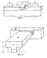
- a MESFET device is shown with substrate 11, typically semi-insulating GaAs, and active layer 12, which is implanted with n-silicon n-type carriers.
- the cap layer 13 for the source/drain contacts is silicon implanted n + .
- the source and drain contacts 14 and 15 are conventional metal materials such as Ti/Pd/Au, Ti/Pt/Au, Al/Ti, Au/Ge.
- the gate is recessed by wet etching a window in layer 13 so that the gate is situated on the active layer 12.
- MESFET devices are typically depletion mode devices with Schottky gates which in contrast with Si MOS transistors are "normally on" devices.
- the Schottky gate for the MESFET device in Fig. 1 is shown at 17, and is made of a conventional contact metal. When reverse biased, n-type carriers are depleted from depletion region 18 beneath the Schottky gate leaving a p-region that pinches off current flow between the source and drain.
- the gate 17 is referred to as T-shaped but is not to be confused with gate configurations, known in the art, that are T-shaped in plan view.
- the gate configuration in Fig. 1, and which describes the objective of the invention, is a vertical T-shape. It can be defined as having a vertical base 21 and a "cross" 22.
- the shape of the gate in a plan view may be square but is conventionally rectangular in shape with the width w of the gate extending into the plane of the figure and typically terminating in a contact pad (not shown) outside the active region of the device.
- Enhancement of the gate conductivity is a function of the increased cross section between the extremities of the gate along the conduction path.
- the important gate dimensions are shown in Fig. 2.
- the objective in these devices is to minimize the gate length l which is the device parameter controlling the frequency response of the transistor.
- the gate length l is reduced to shrink the overall device size the gate resistance along the gate width w increases proportionately.
- the relevant portion of the conduction path i.e. the reduced dimension, extends mainly over the active region from the free end of gate 24 to the gate runner or the contact pad shown generally at 25.
- the contact pad typically is at a different level, i.e. on the field oxide but the levels are omitted for simplicity.
- the enhanced cross section is ( h 2 x l 2 ) - h 1 ( l 2 - l 1 ).
- the gate conductance enhancement factor is 3.
- the gate conductivity is considered enhanced in the context of the invention if the conductance added by the cross of the T-shaped gate contributes an increase of more than 50% to the standard rectangular or square cross sectioned gate. Expressed in terms of the dimensions shown in Fig. 2: ( h 2 x l 2 ) - h 1 ( l 2 - l 1 ) > 1.5 ( l 1 x h 1 )
- the two factors that contribute to the enhancement are h 2 /h 1 and l 2 / l 1 . Both must be greater than unity in a T-shaped structure.
- the variation of the enhancement factor with these ratios can be seen in Fig. 3 where the ratio h 2 /h 1 for several values of l 2 / l 1 is plotted vs. enhancement in percent. It is evident that increasing h 2 /h 1 gives relatively diminishing returns when l 2 / l 1 is low, while increasing the length of the cross of the "T", i.e. increasing l 2 / l 1 , is more effective. To obtain an enhancement factor of greater than 50% l 2 / l 1 should be nearly two or greater.
- a HEMT device is shown in Fig. 4. These devices are similar in appearance to the MESFET of Fig. 1 but are more complex in the internal structure and are designed for lower noise, higher frequency performance, and in special structures, higher power.
- the source and drain contacts 31 and 32 are typically formed on an n + GaAs layer 33 but the Schottky gate in this structure contacts a heterostructure layer 34, e.g. AlGaAs, under contact layer 33.
- the active layer 34 and the depletion region 37 are otherwise similar to corresponding elements in the MESFET.
- Layer 38 is a very thin spacer layer of e.g.
- layer 39 is a buffer layer of undoped GaAs.
- the substrate 41 may be semi-insulating GaAs.
- the T-shaped Schottky gate structure is shown at 42 and is essentially the same as in the MESFET device of Fig. 1.
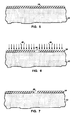
- the technique for fabricating the T-shaped gate structures according to the invention will be described in conjunction with Figs. 5-13.
- the region of the device shown in Figs. 5-13 is the substrate surface between the source and drain electrodes the length of which is exaggerated for illustration.
- the substrate 43 is coated with a first level of photoresist 44.
- the choice of photoresist is not critical and can be any conventional resist material, either positive or negative.
- the length and width of photomask feature 46 correspond to the length and width of the base of the T-shaped gate.
- the pattern can then be developed for 20 seconds using Shipley 321 developer, and then rinsed in D.I. water for 30 seconds. After developing the first level of photoresist window 46 remains as shown in Fig. 7.
- the next step is to harden the surface of the first level photoresist so that it can withstand independent patterning of the second level. This is done by exposure to a plasma which, as shown in Fig. 8, creates a surface layer 47 on the first level photoresist which is durable and is insensitive to subsequent lithographic processing.
- the plasma treatment can create this surface layer without excessive damage to the integrity of the underlying photoresist. It also proceeds at a relatively low temperature, i.e. 50-100 °C..
- a recommended apparatus for the plasma treatment is an electron cyclotron resonance system ( 2.45 GHz ) and a recommended plasma gas is nitrogen. Other plasma gases such as argon, xenon, helium, oxygen, etc. may also give acceptable results.
- the preferred gas is an inert gas.
- Suitable flow rate for nitrogen in the ECR reactor is 2-100 sccm and a suitable power level is 20-500 W.
- Treatment time can vary e.g. between 0.5-5 minutes.
- Appropriate plasma processing conditions are highly dependent on the type of plasma reactor used. However plasma treatments are well developed and well understood and the details of the plasma treatment required to render the first level photoresist insensitive to further actinic processing are within the skill of the art. For the purpose of defining this invention the result of the plasma treatment of the first level photoresist is described as rendering the layer lithographically passive.
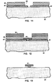
- the next step in the process is to deposit the second level photoresist 48.
- the second level is then patterned as shown in Fig.10.
- the same procedure can be used as in forming the first photoresist layer except that the mask for the second layer has a larger feature 49 which corresponds to l 2 in Fig. 2.
- the thickness t 2 of the second level photoresist layer 48 corresponds to dimension h 2 of Fig. 2 with an excess height added to accommodate the liftoff process as will be described below.
- the thickness t 2 will typically be in the range 0.3-3.0 mm.
- Shipley 1818 was used for the second level photoresist, and was spun at 3000 rpm for 30 seconds giving a photoresist layer thickness of 1.8 mm.
- the layer was prebaked on a hotplate at 110 °C for 60 seconds.
- the exposure time for the Nikon stepper to expose to the bottom of the second photoresist level was 1200 milliseconds.
- the second level photoresist was developed for 20 seconds in Shipley 321 developer and rinsed in D.I. water for 30 seconds.
- the pattern in the first level photoresist remained intact after patterning the second level.
- the resulting structure, shown in Fig. 11, is then ready for metallization to form the T-shaped gate.
- the deposition technique used to deposit the metal, and the composition of the metal are subject to a variety of choices known to those in the art. Evaporation is preferred because it is relatively directional, and therefore is well suited for lift-off processes. Sputtering may also be used. Conformal coating processes such as Chemical Vapor Deposition (CVD), Molecular Beam Epitaxy (MBE) and Atomic Layer Deposition (ALD), are less likely to be effective but ways may be devised by those skilled in the art to adapt these techniques to the process described. In the specific example described here, the preferred deposition technique is evaporation using an e-beam evaporation process.
- the substrate Prior to evaporation the substrate was exposed to a pre-deposit cleaning operation for 3 minutes in an oxygen plasma at 50 watts and 1 torr, followed by a 20:1 HCl:H 2 O rinse for 30 seconds. The surface was blow dried with nitrogen for 30 seconds.
- a suitable metallization for most applications which is well established in this technology, is 250 Angstroms titanium, 500 Angstroms platinum, and 8000 Angstroms gold. After evaporation of the metal the structure appears as in Fig. 12 with the metallization shown at 51 in the gate region and 52 on the surface of the second level resist. A vertical separation between these metal bodies is intentionally created to facilitate the lift-off process as is well known.
- the excess vertical gap between the top surface of the evaporated metal and the top surface of the second level photoresist was approximately 1.4 mm.
Abstract
Description
- This invention relates to methods for the fabrication of field effect transistors with T-shaped gates. It is particularly applicable to Metal-Semiconductor Field Effect Transistor devices (MESFETs) and High Electron Mobility Transistor devices (HEMTs).
- As the feature size in integrated circuits continues to shrink the gate size for transistors must be correspondingly reduced. In state of the art III-V transistor devices the gate size has reached the point where gate resistance due to the small gate dimensions is a performance limiting factor. To overcome this limitation T-shaped gates and Y-shaped gates have been proposed. See e.g. M. H. Somerville et al "A model for Tunneling-Limited Breakdown in High Power HEMTs", IEEE IEDM, pp. 35-38 (1996); F. Ren et aL, "Y-gate submicron gate length GaAs metal-semiconductor field effect transistors", J. Vac. Sci. Technol. B 11(5), Sept./Oct. 1993; A. Mahajan et al, "Monolithic Integration of InAlAs/InGaAs/InP Enhancement- and Depletion-Mode High Electron Mobility Transistors, IEEE IEDM, pp. 51-53, (1996). The T-shaped electrodes for these devices are produced by exposing T-shaped patterns in the resist at the gate location, developing the resist to form T-shaped openings, and evaporating metal into the T-shaped openings. A lift-off process is used to remove excess metal on the resist surface between T-shaped features. The e-beam approach has been successful but the e-beam writing step to form the T-shaped features is slow due to that characteristic raster scan of e-beam lithography, and very expensive. A better approach from the standpoint of throughput would be to use the blanket exposure characteristic of photolithographic processes but to date a photolithographic process for forming a vertically oriented T-shaped feature has not been available in the context of this technology.
- We have developed a photolithographic process for forming T-shaped Schottky gate structures for use in III-V field effect transistor devices. A thick bi-level photoresist layer is used to define T-shaped features, and gate contact metal is deposited in the T-shaped features to form the gate contact structure. The first level resist is patterned and then hardened to withstand the photolithographic patterning step for the second level. The feature in the second level is made to be larger than the first formed feature, thereby producing a structure that is larger at the top than at the base, i.e. a T-shaped structure.
-
- Fig. 1 is a schematic representation of a recessed gate MESFET device with a T-shaped Schottky gate that may be fabricated in accordance with the invention;
- Fig. 2 is a schematic view of a T-shaped gate structure describing the relevant dimensions discussed in this description;
- Fig. 3 is a plot of the relevant dimensions shown in Fig. 2 vs. the enhancement factor in gate conductivity;
- Fig. 4 is a schematic representation of a HEMT device with a T-shaped gate that may be fabricated in accordance with the invention; and
- Figs. 5-13 are representations of process steps used for forming T-shaped gates in accordance with the invention.
-
- Referring to Fig. 1, a MESFET device is shown with
substrate 11, typically semi-insulating GaAs, andactive layer 12, which is implanted with n-silicon n-type carriers. Thecap layer 13 for the source/drain contacts is silicon implanted n+. The source anddrain contacts layer 13 so that the gate is situated on theactive layer 12. MESFET devices are typically depletion mode devices with Schottky gates which in contrast with Si MOS transistors are "normally on" devices. The Schottky gate for the MESFET device in Fig. 1 is shown at 17, and is made of a conventional contact metal. When reverse biased, n-type carriers are depleted fromdepletion region 18 beneath the Schottky gate leaving a p-region that pinches off current flow between the source and drain. - The
gate 17 is referred to as T-shaped but is not to be confused with gate configurations, known in the art, that are T-shaped in plan view. The gate configuration in Fig. 1, and which describes the objective of the invention, is a vertical T-shape. It can be defined as having avertical base 21 and a "cross" 22. The shape of the gate in a plan view may be square but is conventionally rectangular in shape with the width w of the gate extending into the plane of the figure and typically terminating in a contact pad (not shown) outside the active region of the device. - Enhancement of the gate conductivity is a function of the increased cross section between the extremities of the gate along the conduction path. The important gate dimensions are shown in Fig. 2. The objective in these devices is to minimize the gate length l which is the device parameter controlling the frequency response of the transistor. When the gate length l is reduced to shrink the overall device size the gate resistance along the gate width w increases proportionately. The relevant portion of the conduction path, i.e. the reduced dimension, extends mainly over the active region from the free end of
gate 24 to the gate runner or the contact pad shown generally at 25. The contact pad typically is at a different level, i.e. on the field oxide but the levels are omitted for simplicity. If the normal gate cross section is l 1 x h 1, the enhanced cross section is (h 2 x l 2) - h 1 ( l 2 - l 1). For example, if h 2 = 2 h 1 and l 2 = 3l 1, i.e. the approximate geometry shown, then the gate conductance enhancement factor is 3. The gate conductivity is considered enhanced in the context of the invention if the conductance added by the cross of the T-shaped gate contributes an increase of more than 50% to the standard rectangular or square cross sectioned gate. Expressed in terms of the dimensions shown in Fig. 2: - The above expression assumes that the gate height is increased over the standard height. In a more typical case, the dimensions l 1 and h 2 are fixed by the device design and the conventional rectangular gate would have the maximum allowed height, and therefore an effective cross section of h 2 x l 1 . In this case the enhancement is ( l 2 - l 1 ) x ( h 2 - h 1 ). An enhancement of 50% requires:
- The two factors that contribute to the enhancement are h 2 /h 1 and l 2/l 1. Both must be greater than unity in a T-shaped structure. The variation of the enhancement factor with these ratios can be seen in Fig. 3 where the ratio h 2 /h 1 for several values of l 2/l 1 is plotted vs. enhancement in percent. It is evident that increasing h 2 /h 1 gives relatively diminishing returns when l 2/l 1 is low, while increasing the length of the cross of the "T", i.e. increasing l 2/l 1, is more effective. To obtain an enhancement factor of greater than 50% l 2/l 1 should be nearly two or greater.
- Other Schottky gate devices can also take advantage of the enhanced conductivity of T-shaped gates. For example, a HEMT device is shown in Fig. 4. These devices are similar in appearance to the MESFET of Fig. 1 but are more complex in the internal structure and are designed for lower noise, higher frequency performance, and in special structures, higher power. The source and
drain contacts heterostructure layer 34, e.g. AlGaAs, undercontact layer 33. Theactive layer 34 and thedepletion region 37 are otherwise similar to corresponding elements in the MESFET. Layer 38 is a very thin spacer layer of e.g. undoped AlGaAs, andlayer 39 is a buffer layer of undoped GaAs. Thesubstrate 41 may be semi-insulating GaAs. The T-shaped Schottky gate structure is shown at 42 and is essentially the same as in the MESFET device of Fig. 1. - The technique for fabricating the T-shaped gate structures according to the invention will be described in conjunction with Figs. 5-13. For simplicity in describing the processing the substrate and the functional layers in the substrate will be omitted, the assumption being that these device features are complete at the point in the process where gate fabrication commences. The region of the device shown in Figs. 5-13 is the substrate surface between the source and drain electrodes the length of which is exaggerated for illustration. Referring to Fig. 5 the
substrate 43 is coated with a first level ofphotoresist 44. The choice of photoresist is not critical and can be any conventional resist material, either positive or negative. In the work described here Shipley 1805 photoresist was spun on the wafer at 3000 rpm for 30 seconds to produce a photoresist layer of 0.5 mm in thickness, and the layer was prebaked on a hotplate at 110 °C for 60 seconds. The thickness t 1 of the first level of photoresist corresponds to dimension h 1 of Fig. 2, and is preferably in the range 0.2 - 2.0 mm. Thephotoresist layer 44 is exposed toactinic radiation 45 through a photomask withfeature 46 using standard practice as shown in Fig. 6. For the Shipley photoresist mentioned above exposure using a Nikon stepper at 436 nm wavelength for 750 milliseconds is effective. The length and width ofphotomask feature 46 correspond to the length and width of the base of the T-shaped gate. The pattern can then be developed for 20 seconds using Shipley 321 developer, and then rinsed in D.I. water for 30 seconds. After developing the first level ofphotoresist window 46 remains as shown in Fig. 7. - The next step is to harden the surface of the first level photoresist so that it can withstand independent patterning of the second level. This is done by exposure to a plasma which, as shown in Fig. 8, creates a
surface layer 47 on the first level photoresist which is durable and is insensitive to subsequent lithographic processing. The plasma treatment can create this surface layer without excessive damage to the integrity of the underlying photoresist. It also proceeds at a relatively low temperature, i.e. 50-100 °C.. A recommended apparatus for the plasma treatment is an electron cyclotron resonance system ( 2.45 GHz ) and a recommended plasma gas is nitrogen. Other plasma gases such as argon, xenon, helium, oxygen, etc. may also give acceptable results. The preferred gas is an inert gas. Suitable flow rate for nitrogen in the ECR reactor is 2-100 sccm and a suitable power level is 20-500 W. Treatment time can vary e.g. between 0.5-5 minutes. Appropriate plasma processing conditions are highly dependent on the type of plasma reactor used. However plasma treatments are well developed and well understood and the details of the plasma treatment required to render the first level photoresist insensitive to further actinic processing are within the skill of the art. For the purpose of defining this invention the result of the plasma treatment of the first level photoresist is described as rendering the layer lithographically passive. - With reference to Fig. 9, the next step in the process is to deposit the
second level photoresist 48. The second level is then patterned as shown in Fig.10. The same procedure can be used as in forming the first photoresist layer except that the mask for the second layer has alarger feature 49 which corresponds to l 2 in Fig. 2. The thickness t2 of the secondlevel photoresist layer 48 corresponds to dimension h 2 of Fig. 2 with an excess height added to accommodate the liftoff process as will be described below. The thickness t 2 will typically be in the range 0.3-3.0 mm. In our work Shipley 1818 was used for the second level photoresist, and was spun at 3000 rpm for 30 seconds giving a photoresist layer thickness of 1.8 mm. The layer was prebaked on a hotplate at 110 °C for 60 seconds. The exposure time for the Nikon stepper to expose to the bottom of the second photoresist level was 1200 milliseconds. The second level photoresist was developed for 20 seconds in Shipley 321 developer and rinsed in D.I. water for 30 seconds. The pattern in the first level photoresist remained intact after patterning the second level. - The resulting structure, shown in Fig. 11, is then ready for metallization to form the T-shaped gate. The deposition technique used to deposit the metal, and the composition of the metal are subject to a variety of choices known to those in the art. Evaporation is preferred because it is relatively directional, and therefore is well suited for lift-off processes. Sputtering may also be used. Conformal coating processes such as Chemical Vapor Deposition (CVD), Molecular Beam Epitaxy (MBE) and Atomic Layer Deposition (ALD), are less likely to be effective but ways may be devised by those skilled in the art to adapt these techniques to the process described. In the specific example described here, the preferred deposition technique is evaporation using an e-beam evaporation process. Prior to evaporation the substrate was exposed to a pre-deposit cleaning operation for 3 minutes in an oxygen plasma at 50 watts and 1 torr, followed by a 20:1 HCl:H2O rinse for 30 seconds. The surface was blow dried with nitrogen for 30 seconds.. A suitable metallization for most applications, which is well established in this technology, is 250 Angstroms titanium, 500 Angstroms platinum, and 8000 Angstroms gold. After evaporation of the metal the structure appears as in Fig. 12 with the metallization shown at 51 in the gate region and 52 on the surface of the second level resist. A vertical separation between these metal bodies is intentionally created to facilitate the lift-off process as is well known. In the process described the excess vertical gap between the top surface of the evaporated metal and the top surface of the second level photoresist was approximately 1.4 mm. An acceptable difference between the thickness of the metal layer (h 1 + h 2) and the combined thickness, t 1 + t 2 , of the bi-level resist is at least 30%, i.e. t 1 + t 2 = 1.3 (h 1 + h 2), and preferably at least 100%, i.e. t 1 + t 2 = 2 (h 1 + h 2).
- The two levels of resist 42 and 46, carrying the surface layer of
unwanted metal 52 are then dissolved in a solvent such as acetone, leaving the final structure as shown in Fig. 13.
Claims (7)
- A method for the manufacture of a Schottky gate transistor comprising the steps of:forming a source and drain in a III-V semiconductor substrate, andforming a Schottky gate on the surface of said III-V semiconductorbetween said source and drainthe invention characterized in that said Schottky gate is formed by the steps comprising:a. depositing a first level of photoresist on the surface of said substrate, said first level of photoresist having a thickness t 1,b. lithographically forming an opening in said first level of photoresist, said opening having a rectangular shape with width w 1 and length l 1 , with the length dimension extending along the direction separating the source and drain,c. exposing said first level of photoresist to a plasma to form a surface layer on said first level of photoresist to harden said surface layer and render it lithographically passive,d. depositing a second level of photoresist on said first level of photoresist, said second level of photoresist having a thickness t 2 ,e. lithographically forming an opening in said second level of photoresist, said opening coinciding with said opening in said first level of photoresist and having a rectangular shape with width w2 and length l 2, and further where length l 2 is greater than length l 1,f. depositing a metal layer to fill said first opening and to fill a portion of said second opening, said metal layer having a thickness h 1 + h 2, where h 1 is essentially equal to t 1 and h 2 is substantially less than t 2 ,g. and dissolving away said first and second level of photoresist leaving a T-shaped Schottky gate.
- The method of claim 1 wherein said Schottky gate transistor is a MESFET.
- The method of claim 1 wherein said Schottky gate transistor is a HEMT.
- The method of claim 1 in which l 2 is at least twice l 1.
- The method of claim 1 wherein the dimensions l 1, l 2, h1 and h2 are related by:
- The method of claim 5 wherein w 1 is approximately equal to w 2.
- A method for the manufacture of a Schottky gate transistor comprising the steps of:forming a source and drain in a III-V semiconductor substrate, andforming a Schottky gate on the surface of said III-V semiconductorsubstrate between said source and drain,the invention characterized in that said Schottky gate is T-shaped with the base of the T having height h 1 and the cross of the T having height h 2 said T-shaped gate being formed by the steps comprising:a. depositing a first level of photoresist on the surface of said substrate, said first level of photoresist having a thickness t 1 in the range 0.2 - 2.0 mm, said thickness t 1 being equal to h 1,b. photolithographically forming an opening in said first level of photoresist, said opening having a rectangular shape with width w 1 and length l 1, with the length dimension extending along the direction separating the source and drain,c. placing said substrate in an electron cyclotron resonance plasma reactor and exposing said first level of photoresist to an inert gas plasma at a temperature below 100 °C to form a surface layer on said first level of photoresist to harden said surface layer and render it photolithographically passive,d. depositing a second level of photoresist on said first level of photoresist, said second level of photoresist having a thickness t 2 in the range 0.3 - 3.0 mm, said thickness t 2 being substantially greater than h 2,e. photolithographically forming an opening in said second level of photoresist, said opening coinciding with said opening in said first level of photoresist and having a rectangular shape with width w 2 and length l 2, and further where length l 2 is at least twice length l 1,f. depositing a metal layer by evaporating metal to fill said first opening and to fill a portion of said second opening, said metal layer having a thickness h 1 + h 2, where t 1 + t 2 is at least 2 times h 1 + h 2 ,g. and dissolving away said first and second level of photoresist leaving a T-shaped Schottky gate.
Applications Claiming Priority (2)
| Application Number | Priority Date | Filing Date | Title |
|---|---|---|---|
| US08/935,121 US5981319A (en) | 1997-09-22 | 1997-09-22 | Method of forming a T-shaped gate |
| US935121 | 1997-09-22 |
Publications (2)
| Publication Number | Publication Date |
|---|---|
| EP0903779A2 true EP0903779A2 (en) | 1999-03-24 |
| EP0903779A3 EP0903779A3 (en) | 2000-11-22 |
Family
ID=25466608
Family Applications (1)
| Application Number | Title | Priority Date | Filing Date |
|---|---|---|---|
| EP98307228A Withdrawn EP0903779A3 (en) | 1997-09-22 | 1998-09-08 | Manufacture of field effect transistors |
Country Status (3)
| Country | Link |
|---|---|
| US (1) | US5981319A (en) |
| EP (1) | EP0903779A3 (en) |
| JP (1) | JPH11150130A (en) |
Cited By (2)
| Publication number | Priority date | Publication date | Assignee | Title |
|---|---|---|---|---|
| WO2005081299A2 (en) * | 2004-02-23 | 2005-09-01 | Asml Netherlands B.V. | Device manufacturing method and substrate comprising radiation sensitive material |
| CN110429063A (en) * | 2019-06-28 | 2019-11-08 | 福建省福联集成电路有限公司 | A kind of method, semi-conductor device manufacturing method and device of noise values |
Families Citing this family (14)
| Publication number | Priority date | Publication date | Assignee | Title |
|---|---|---|---|---|
| US7008832B1 (en) | 2000-07-20 | 2006-03-07 | Advanced Micro Devices, Inc. | Damascene process for a T-shaped gate electrode |
| US6403456B1 (en) * | 2000-08-22 | 2002-06-11 | Advanced Micro Devices, Inc. | T or T/Y gate formation using trim etch processing |
| US6355561B1 (en) | 2000-11-21 | 2002-03-12 | Micron Technology, Inc. | ALD method to improve surface coverage |
| US6541361B2 (en) * | 2001-06-27 | 2003-04-01 | Lam Research Corp. | Plasma enhanced method for increasing silicon-containing photoresist selectivity |
| JP2003142500A (en) * | 2001-10-30 | 2003-05-16 | Fujitsu Ltd | Method for manufacturing semiconductor device |
| US6737202B2 (en) * | 2002-02-22 | 2004-05-18 | Motorola, Inc. | Method of fabricating a tiered structure using a multi-layered resist stack and use |
| RU2216818C1 (en) * | 2003-01-28 | 2003-11-20 | Общество с ограниченной ответственностью "ЭпиЛаб" | Electron cyclotron resonance -plasma source to process semiconductor structures, method to process semiconductor structures, process of manufacture of semiconductor devices and integrated circuits ( variants ), semiconductor device or integrated circuit ( variants ) |
| US7132372B2 (en) * | 2004-07-29 | 2006-11-07 | Freescale Semiconductor, Inc. | Method for preparing a semiconductor substrate surface for semiconductor device fabrication |
| US7439166B1 (en) | 2005-06-11 | 2008-10-21 | Hrl Laboratories, Llc | Method for producing tiered gate structure devices |
| US7608497B1 (en) | 2006-09-08 | 2009-10-27 | Ivan Milosavljevic | Passivated tiered gate structure transistor and fabrication method |
| US7692222B2 (en) * | 2006-11-07 | 2010-04-06 | Raytheon Company | Atomic layer deposition in the formation of gate structures for III-V semiconductor |
| CN102513242B (en) | 2009-03-27 | 2016-01-20 | 三菱电机株式会社 | Atomising device, equipment, air regulator and refrigerator |
| CN103700583A (en) * | 2014-01-06 | 2014-04-02 | 中国科学院微电子研究所 | Manufacturing method of T-shaped gate of GaN-based FET (Field Effect Transistor) |
| US9379327B1 (en) * | 2014-12-16 | 2016-06-28 | Carbonics Inc. | Photolithography based fabrication of 3D structures |
Citations (4)
| Publication number | Priority date | Publication date | Assignee | Title |
|---|---|---|---|---|
| JPH0265139A (en) * | 1988-08-30 | 1990-03-05 | Toshiba Corp | Method of forming electrode for semiconductor device |
| JPH0590300A (en) * | 1991-09-30 | 1993-04-09 | Fujitsu Ltd | Manufacture of semiconductor device |
| US5370973A (en) * | 1991-11-12 | 1994-12-06 | Matsushita Electric Industrial Co., Ltd. | Method of fabricating a fine structure electrode |
| US5583063A (en) * | 1993-11-30 | 1996-12-10 | Nec Corporation | Method of forming T-shaped, cross-sectional pattern using two layered masks |
Family Cites Families (6)
| Publication number | Priority date | Publication date | Assignee | Title |
|---|---|---|---|---|
| JPH02266535A (en) * | 1989-04-07 | 1990-10-31 | Sony Corp | Manufacture of field-effect semiconductor device |
| JPH05235055A (en) * | 1992-02-25 | 1993-09-10 | Sony Corp | Compound semiconductor device |
| US5693548A (en) * | 1994-12-19 | 1997-12-02 | Electronics And Telecommunications Research Institute | Method for making T-gate of field effect transistor |
| US5776805A (en) * | 1995-12-29 | 1998-07-07 | Lg Semicon Co., Ltd. | Method for manufacturing MESFET |
| TW301061B (en) * | 1996-06-07 | 1997-03-21 | Ind Tech Res Inst | Manufacturing method of submicron T-type gate |
| JP2780704B2 (en) * | 1996-06-14 | 1998-07-30 | 日本電気株式会社 | Method for manufacturing semiconductor device |
-
1997
- 1997-09-22 US US08/935,121 patent/US5981319A/en not_active Expired - Lifetime
-
1998
- 1998-09-08 EP EP98307228A patent/EP0903779A3/en not_active Withdrawn
- 1998-09-21 JP JP10267052A patent/JPH11150130A/en active Pending
Patent Citations (4)
| Publication number | Priority date | Publication date | Assignee | Title |
|---|---|---|---|---|
| JPH0265139A (en) * | 1988-08-30 | 1990-03-05 | Toshiba Corp | Method of forming electrode for semiconductor device |
| JPH0590300A (en) * | 1991-09-30 | 1993-04-09 | Fujitsu Ltd | Manufacture of semiconductor device |
| US5370973A (en) * | 1991-11-12 | 1994-12-06 | Matsushita Electric Industrial Co., Ltd. | Method of fabricating a fine structure electrode |
| US5583063A (en) * | 1993-11-30 | 1996-12-10 | Nec Corporation | Method of forming T-shaped, cross-sectional pattern using two layered masks |
Non-Patent Citations (3)
| Title |
|---|
| LOTHIAN J R ET AL: "A novel bi-layer photoresist T-gate technique to reduce gate resistance" POWER SEMICONDUCTOR MATERIALS AND DEVICES SYMPOSIUM, BOSTON, MA, USA, 1 - 4 December 1997, pages 271-275, XP000911818 Mater. Res. Soc., Warrendale, PA, USA * |
| PATENT ABSTRACTS OF JAPAN vol. 014, no. 239 (E-0930), 21 May 1990 (1990-05-21) & JP 02 065139 A (TOSHIBA CORP), 5 March 1990 (1990-03-05) -& JP 02 065139 A (TOSHIBA CORP) 5 March 1990 (1990-03-05) * |
| PATENT ABSTRACTS OF JAPAN vol. 017, no. 431 (E-1411), 10 August 1993 (1993-08-10) & JP 05 090300 A (FUJITSU LTD), 9 April 1993 (1993-04-09) -& JP 05 090300 A (FUJITSU LTD) 9 April 1993 (1993-04-09) * |
Cited By (4)
| Publication number | Priority date | Publication date | Assignee | Title |
|---|---|---|---|---|
| WO2005081299A2 (en) * | 2004-02-23 | 2005-09-01 | Asml Netherlands B.V. | Device manufacturing method and substrate comprising radiation sensitive material |
| WO2005081299A3 (en) * | 2004-02-23 | 2006-03-09 | Asml Netherlands Bv | Device manufacturing method and substrate comprising radiation sensitive material |
| US7892903B2 (en) | 2004-02-23 | 2011-02-22 | Asml Netherlands B.V. | Device manufacturing method and substrate comprising multiple resist layers |
| CN110429063A (en) * | 2019-06-28 | 2019-11-08 | 福建省福联集成电路有限公司 | A kind of method, semi-conductor device manufacturing method and device of noise values |
Also Published As
| Publication number | Publication date |
|---|---|
| US5981319A (en) | 1999-11-09 |
| EP0903779A3 (en) | 2000-11-22 |
| JPH11150130A (en) | 1999-06-02 |
Similar Documents
| Publication | Publication Date | Title |
|---|---|---|
| US6139995A (en) | Method of manufacturing schottky gate transistor utilizing alignment techniques with multiple photoresist layers | |
| US5155053A (en) | Method of forming t-gate structure on microelectronic device substrate | |
| US5981319A (en) | Method of forming a T-shaped gate | |
| US5270228A (en) | Method of fabricating gate electrode in recess | |
| US6204102B1 (en) | Method of fabricating compound semiconductor devices using lift-off of insulating film | |
| US5399896A (en) | FET with a T-shaped gate of a particular structure | |
| US5112763A (en) | Process for forming a Schottky barrier gate | |
| EP0810645B1 (en) | Method of fabricating double photoresist layer self-aligned heterojunction bipolar transistor | |
| US6294446B1 (en) | Methods of manufacturing a high electron mobility transistor with a T-shaped gate electrode | |
| US5587328A (en) | Method for manufacturing semiconductor device | |
| Chang et al. | Submicron T-shaped gate HEMT fabrication using deep-UV lithography | |
| US5231040A (en) | Method of making a field effect transistor | |
| US4935377A (en) | Method of fabricating microwave FET having gate with submicron length | |
| US5970328A (en) | Fabrication method of T-shaped gate electrode in semiconductor device | |
| US5483089A (en) | Electrically isolated MESFET | |
| Lee et al. | Pseudomorphic AlGaAs/InGaAs/GaAs high electron mobility transistors with super low noise performances of 0.41 dB at 18 GHz | |
| JPS6341078A (en) | Manufacture of semiconductor device | |
| JP2004363150A (en) | Method of forming pattern | |
| EP0613174A2 (en) | Method for making fine-line semiconductor devices | |
| KR100264532B1 (en) | Method for forming fets having their respective mode or threshold voltage | |
| KR19990075338A (en) | T-gate fabrication method of a water-doped high electron mobility transistor | |
| JP2906856B2 (en) | Method for manufacturing field effect transistor | |
| EP0366939A2 (en) | A process for forming a Schottky barrier gate on gallium-arsenide | |
| JPH0846146A (en) | Fabrication of semiconductor integrated circuit | |
| JPS616870A (en) | Manufacture of field-effect transistor |
Legal Events
| Date | Code | Title | Description |
|---|---|---|---|
| PUAI | Public reference made under article 153(3) epc to a published international application that has entered the european phase |
Free format text: ORIGINAL CODE: 0009012 |
|
| AK | Designated contracting states |
Kind code of ref document: A2 Designated state(s): DE FR GB |
|
| AX | Request for extension of the european patent |
Free format text: AL;LT;LV;MK;RO;SI |
|
| PUAL | Search report despatched |
Free format text: ORIGINAL CODE: 0009013 |
|
| AK | Designated contracting states |
Kind code of ref document: A3 Designated state(s): AT BE CH CY DE DK ES FI FR GB GR IE IT LI LU MC NL PT SE |
|
| AX | Request for extension of the european patent |
Free format text: AL;LT;LV;MK;RO;SI |
|
| 17P | Request for examination filed |
Effective date: 20010518 |
|
| AKX | Designation fees paid |
Free format text: DE FR GB |
|
| STAA | Information on the status of an ep patent application or granted ep patent |
Free format text: STATUS: THE APPLICATION IS DEEMED TO BE WITHDRAWN |
|
| 18D | Application deemed to be withdrawn |
Effective date: 20060628 |