EP0902843B1 - Procede de realisation d'un film mince de materiau solide et applications de ce procede - Google Patents
Procede de realisation d'un film mince de materiau solide et applications de ce procede Download PDFInfo
- Publication number
- EP0902843B1 EP0902843B1 EP97924080A EP97924080A EP0902843B1 EP 0902843 B1 EP0902843 B1 EP 0902843B1 EP 97924080 A EP97924080 A EP 97924080A EP 97924080 A EP97924080 A EP 97924080A EP 0902843 B1 EP0902843 B1 EP 0902843B1
- Authority
- EP
- European Patent Office
- Prior art keywords
- substrate
- support
- thin film
- face
- ions
- Prior art date
- Legal status (The legal status is an assumption and is not a legal conclusion. Google has not performed a legal analysis and makes no representation as to the accuracy of the status listed.)
- Expired - Lifetime
Links
Images

Classifications
-
- C—CHEMISTRY; METALLURGY
- C23—COATING METALLIC MATERIAL; COATING MATERIAL WITH METALLIC MATERIAL; CHEMICAL SURFACE TREATMENT; DIFFUSION TREATMENT OF METALLIC MATERIAL; COATING BY VACUUM EVAPORATION, BY SPUTTERING, BY ION IMPLANTATION OR BY CHEMICAL VAPOUR DEPOSITION, IN GENERAL; INHIBITING CORROSION OF METALLIC MATERIAL OR INCRUSTATION IN GENERAL
- C23C—COATING METALLIC MATERIAL; COATING MATERIAL WITH METALLIC MATERIAL; SURFACE TREATMENT OF METALLIC MATERIAL BY DIFFUSION INTO THE SURFACE, BY CHEMICAL CONVERSION OR SUBSTITUTION; COATING BY VACUUM EVAPORATION, BY SPUTTERING, BY ION IMPLANTATION OR BY CHEMICAL VAPOUR DEPOSITION, IN GENERAL
- C23C14/00—Coating by vacuum evaporation, by sputtering or by ion implantation of the coating forming material
- C23C14/22—Coating by vacuum evaporation, by sputtering or by ion implantation of the coating forming material characterised by the process of coating
- C23C14/48—Ion implantation
-
- C—CHEMISTRY; METALLURGY
- C23—COATING METALLIC MATERIAL; COATING MATERIAL WITH METALLIC MATERIAL; CHEMICAL SURFACE TREATMENT; DIFFUSION TREATMENT OF METALLIC MATERIAL; COATING BY VACUUM EVAPORATION, BY SPUTTERING, BY ION IMPLANTATION OR BY CHEMICAL VAPOUR DEPOSITION, IN GENERAL; INHIBITING CORROSION OF METALLIC MATERIAL OR INCRUSTATION IN GENERAL
- C23C—COATING METALLIC MATERIAL; COATING MATERIAL WITH METALLIC MATERIAL; SURFACE TREATMENT OF METALLIC MATERIAL BY DIFFUSION INTO THE SURFACE, BY CHEMICAL CONVERSION OR SUBSTITUTION; COATING BY VACUUM EVAPORATION, BY SPUTTERING, BY ION IMPLANTATION OR BY CHEMICAL VAPOUR DEPOSITION, IN GENERAL
- C23C14/00—Coating by vacuum evaporation, by sputtering or by ion implantation of the coating forming material
- C23C14/58—After-treatment
-
- H—ELECTRICITY
- H01—ELECTRIC ELEMENTS
- H01L—SEMICONDUCTOR DEVICES NOT COVERED BY CLASS H10
- H01L21/00—Processes or apparatus adapted for the manufacture or treatment of semiconductor or solid state devices or of parts thereof
- H01L21/70—Manufacture or treatment of devices consisting of a plurality of solid state components formed in or on a common substrate or of parts thereof; Manufacture of integrated circuit devices or of parts thereof
- H01L21/71—Manufacture of specific parts of devices defined in group H01L21/70
- H01L21/76—Making of isolation regions between components
- H01L21/762—Dielectric regions, e.g. EPIC dielectric isolation, LOCOS; Trench refilling techniques, SOI technology, use of channel stoppers
- H01L21/7624—Dielectric regions, e.g. EPIC dielectric isolation, LOCOS; Trench refilling techniques, SOI technology, use of channel stoppers using semiconductor on insulator [SOI] technology
- H01L21/76251—Dielectric regions, e.g. EPIC dielectric isolation, LOCOS; Trench refilling techniques, SOI technology, use of channel stoppers using semiconductor on insulator [SOI] technology using bonding techniques
- H01L21/76254—Dielectric regions, e.g. EPIC dielectric isolation, LOCOS; Trench refilling techniques, SOI technology, use of channel stoppers using semiconductor on insulator [SOI] technology using bonding techniques with separation/delamination along an ion implanted layer, e.g. Smart-cut, Unibond
-
- H—ELECTRICITY
- H01—ELECTRIC ELEMENTS
- H01L—SEMICONDUCTOR DEVICES NOT COVERED BY CLASS H10
- H01L28/00—Passive two-terminal components without a potential-jump or surface barrier for integrated circuits; Details thereof; Multistep manufacturing processes therefor
- H01L28/40—Capacitors
- H01L28/55—Capacitors with a dielectric comprising a perovskite structure material
-
- H—ELECTRICITY
- H10—SEMICONDUCTOR DEVICES; ELECTRIC SOLID-STATE DEVICES NOT OTHERWISE PROVIDED FOR
- H10B—ELECTRONIC MEMORY DEVICES
- H10B53/00—Ferroelectric RAM [FeRAM] devices comprising ferroelectric memory capacitors
-
- H—ELECTRICITY
- H10—SEMICONDUCTOR DEVICES; ELECTRIC SOLID-STATE DEVICES NOT OTHERWISE PROVIDED FOR
- H10B—ELECTRONIC MEMORY DEVICES
- H10B53/00—Ferroelectric RAM [FeRAM] devices comprising ferroelectric memory capacitors
- H10B53/30—Ferroelectric RAM [FeRAM] devices comprising ferroelectric memory capacitors characterised by the memory core region
Definitions
- the present invention relates to a method making a thin film of solid material
- this material can be a dielectric, a conductor or a semi-insulator. It can be crystalline or not. It can be an amorphous semiconductor or polycrystalline whose crystallographic planes are of any orientation. This material may have ferroelectric, piezoelectric properties, magnetic, electro-optical, etc.
- a particularly interesting application of the method according to the invention relates to the production of ferroelectric capacitor memories.
- This implantation is able to create a layer of gaseous microbubbles which will end at the end of heat treatment at a fracture zone.
- This layer of microbubbles thus created in the volume of the plate, at a depth close to the depth mean ion penetration, delimits in the volume of the wafer two regions separated by this layer: a region intended to constitute the thin film and a region forming the remainder of the substrate.
- the heat treatment is carried out at a temperature sufficient to create, by effect of crystalline rearrangement in the material semiconductor such as for example by effect of growth of microcavities and / or by pressure effect microbubbles, fracture zone and separation between the two regions.
- cavities or microbubbles are observable or not in transmission electron microscopy.
- a gas such as hydrogen
- microcavities whose size can vary from a few nm to a few hundred nm. So especially when the temperature implantation is weak, these cavities are only observable that during the treatment stage thermal, stage during which one then realizes nucleation to allow completion at the end of heat treatment at the fracture between the thin film and the rest of the substrate.
- the first step in ion implantation is conducted by presenting a plane face to an ion beam of a wafer of semiconductor material, the plan of this planar face being either substantially parallel to a main crystallographic plane in the case where the semiconductor material is perfectly monocrystalline, or slightly inclined relative to to a main crystallographic plane of the same indices for all the grains in the case where the material is polycrystalline.
- gas microbubbles means any cavity or microcavity generated by the implantation of gas ions hydrogen or rare gases in the material.
- the cavities can be very flattened, that is to say of low height, for example of the order of some inter-atomic distances, as well as in substantially spherical form or in any other different form from the two previous forms.
- cavities may or may not contain a free gas phase and / or gas atoms from fixed implanted ions on atoms of the material forming the walls of cavities. These cavities are generally called in English terminology “platelets”, “microblisters” or even “bubbles”.
- the heat treatment is carried out at a temperature sufficient (for the duration of the treatment applied) for create separation between the two regions. The couple time and temperature of heat treatment depends of the dose of implanted ions.
- the process described in the document FR-A-2 681 472 relates to the making of a film thin from a substrate of semiconductor material of crystal structure.
- the progress of the different process steps have been explained as resulting from the interaction between implanted ions and the mesh of the semiconductor material.
- the inventors of the present invention have was surprised to find that the implantation of ions hydrogen gas or rare gases can also cause the formation of microcavities in solid materials other than a crystalline semiconductor material, and that a subsequent heat treatment can cause the separation, at the level of the microcavities, of the mass material in two parts. Indeed, the treatment thermal conduct, regardless of the type of material solid, to the coalescence of the microcavities which bring a weakening of the structure at the level of the layer of microcavities. This embrittlement allows the separation of the material under the effect of constraints internal and / or pressure in the microcavities, this separation can be natural or assisted by application of external constraints.
- layer of microcavities is meant a area containing microcavities that can be located different depths and can be adjacent or not between them.
- This optional step can be necessary in case the thin layer is not sufficiently rigid by itself. She may be desired since, generally, the thin layer is intended to be placed on a support. In that case, the support must be able to withstand the processing step final thermal.
- the fixing of said face of the substrate on the support can be done by means of a substance adhesive or by means of a treatment favoring interatomic bonds.
- This method according to the invention applies especially for obtaining a thin film of material ferroelectric, from a material substrate ferroelectric, and its attachment to a support.
- the support being made of material semiconductor, at least one control circuit electronics is developed on one side of this support, the thin film of ferroelectric material is fixed on the support so as to serve as a dielectric to a memory capacity controlled by said circuit electronic control to constitute a point memory.
- control circuit electronics is of the MOS transistor type.
- the method according to the invention can also be applied to obtain a thin film of sapphire on a support, a thin film of corrosion-resistant metal on a support or a thin film of magnetic material on a support.
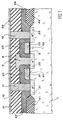
- the electronic circuit shown in section in Figure 1 was carried out according to the techniques current micro-electronics. We implemented the so-called “plug” technique, the planarization technique mechanochemistry of oxides and the so-called technique “Damascene” allowing connections to be made buried in an oxide but flush with the surface of it.
- the circuit was developed on one side 2 of a P-type silicon substrate 1. From side 2, boxes were made, only boxes N, 31 and 32 and type N + being represented in this figure, and field oxide was grown to obtain isolation zones 41 and 42 to the left of the box 31 and to the right of the box 33.
- the boxes 31 and 33 are intended to constitute the drains of two MOS type transistors , the box 32 constituting their common source.
- word lines 51 and 52 of polycrystalline silicon have been deposited, with the interposition of thin oxide layers 61 and 62.
- Word lines 51 and 52 have been covered with layers of insulating material 65 and 66. This insulating material also covers the zones 41 and 42 in the form of layers 63 and 64.
- a line of aluminum bits 8 provides electrical contact with the source 32.
- An oxide layer 7 has been deposited to cover all of the elements described previously.
- the oxide layer 7 are deposited flush electrodes 91 and 92 made of platinum and provided with TiN barrier sublayers.
- the electrodes 91 and 92 are connected by "plugs" 11 and 12 to the drains 31 and 33 of the transistors. They are buried, the circuit then having an external planar face 15.
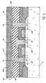
- FIG. 2 represents, seen from the side, a substrate 100 made of ferroelectric material, for example made of PbZrTiO 3 (PZT).
- the flat face 101 of the substrate 100 is bombarded with ions, for example hydrogen ions with an energy of 200 keV and at a dose equal to 10 17 cm -2 .
- the ion bombardment is represented by arrows in FIG. 2.
- the implanted ions induce microcavities which are distributed in a layer 102 in the vicinity of a plane parallel to the plane face 101, this plane being located at a distance from the plane face. 101 corresponding to the average depth of penetration of the ions.
- the thickness of region 103 is about 800 nm.
- Layer 102 is formed by a layer of microcavities.
- FIG. 1 shows the two substrates 100 and 1 associated, the flat face 15 of the substrate semiconductor 1 adhering to the flat face 101 of the substrate 100 made of ferroelectric material.
- the outer face 105 of the thin film 103 is possibly finely polished.
- Such a ferroelectric thin film can also be used to form a layer of ferroelectric material deposited directly on the silicon to make MOS transistors where the gate is replaced by this layer ferroelectric whose polarization state determines the off or on state of the transistor.
- the application of the method according to the invention to dielectric materials makes it possible in particular to produce anti-wear layers of sapphire ( ⁇ -alumina) on glass or silica supports.
- ⁇ -alumina sapphire
- Such a thin layer of alumina makes it possible to protect the glass or the silica serving as a support, for example for optical components, from wear and scratches.
- An implantation of hydrogen ions of approximately 8.10 16 atoms / cm 2 and 110 keV of energy makes it possible to obtain a thin layer or sapphire of approximately 1 ⁇ m in thickness. This small thickness is compatible with any subsequent shaping of the glass or of the silica serving as a support for producing optics, for example.
- the method according to the invention also applies to metallic materials. It makes it possible to produce anti-corrosion layers and diffusion barriers.
- the possibility of producing metallic monocrystalline layers instead of polycrystalline layers provides a significant advantage in terms of effectiveness as a diffusion barrier to chemical attack and to corrosion in particular. Indeed, the existence of significant diffusion phenomena at grain boundaries, in polycrystalline materials, limits the effectiveness of the thin layers produced in these materials.
- Another example of application concerns the production of memories using, for storage information, magnetic domains (bubbles) and the walls of magnetic domains (Bloch walls).
- magnetic domains bubbles
- Bloch walls the walls of magnetic domains
- the process according to the invention makes it possible to transfer a thin layer of ferrimagnetic garnet material on a substrate made of silicon serving as support and comprising integrated circuits.
- integrated circuits combine electronic, logic and analog devices, integrated micro-windings capable of generating fields magnetic located so as to drive, move and detect magnetic fields or walls areas in the thin garnet layer ferrimagnetic.
Landscapes
- Chemical & Material Sciences (AREA)
- Engineering & Computer Science (AREA)
- Power Engineering (AREA)
- Materials Engineering (AREA)
- Chemical Kinetics & Catalysis (AREA)
- Mechanical Engineering (AREA)
- Metallurgy (AREA)
- Organic Chemistry (AREA)
- Computer Hardware Design (AREA)
- Microelectronics & Electronic Packaging (AREA)
- Physics & Mathematics (AREA)
- Condensed Matter Physics & Semiconductors (AREA)
- General Physics & Mathematics (AREA)
- Manufacturing & Machinery (AREA)
- Semiconductor Memories (AREA)
- Semiconductor Integrated Circuits (AREA)
- Thin Film Transistor (AREA)
Abstract
Description
- une première étape d'implantation par bombardement de la face plane de la plaquette au moyen d'ions créant, dans le volume de la plaquette et à une profondeur voisine de la profondeur de pénétration des ions, une couche de "microbulle gazeuse" séparant la plaquette en une région inférieure constituant la masse du substrat et une région supérieure constituant le film mince, les ions étant choisis parmi les ions de gaz rares ou de gaz hydrogène ;
- une deuxième étape de mise en contact intime de la face plane de la plaquette avec un support constitué au moins d'une couche de matériau rigide. Ce contact intime pouvant être réalisé par exemple à l'aide d'une substance adhésive ou par l'effet d'une préparation préalable des surfaces et éventuellement d'un traitement thermique ou/et électrostatique pour favoriser les liaisons interatomiques entre le support et la plaquette ;
- une troisième étape de traitement thermique de l'ensemble plaquette et support à une température supérieure à la température durant laquelle l'implantation a été effectuée et suffisante pour créer une séparation entre le film mince et la masse du substrat. Cette température est supérieure ou égale à environ 400°C pour le silicium.
- une étape d'implantation ionique au cours de laquelle une face du substrat est bombardée par des ions choisis parmi les ions de gaz rares et de gaz hydrogène, afin de créer, dans le volume du substrat et à une profondeur voisine de la profondeur moyenne de pénétration des ions, une couche de microcavités séparant le substrat en deux régions,
- une étape de traitement thermique destinée à porter la couche de microcavités à une température suffisante pour provoquer une séparation encre les deux régions du substrat soit naturellement, soit avec l'aide d'une contrainte appliquée,
- et optionnellement, entre l'étape d'implantation ionique et l'étape de traitement thermique, il est prévu une étape de fixation de ladite face du substrat sur un support.
- la figure 1 est une vue partielle en coupe transversale d'un circuit intégré réalisé sur une face d'un substrat semiconducteur,
- la figure 2 illustre l'étape d'implantation ionique effectuée au travers d'une face d'un substrat en matériau ferroélectrique, selon la présente invention,
- la figure 3 illustre l'étape de fixation selon la présente invention, consistant à faire adhérer la face du substrat semiconducteur où le circuit intégré a été réalisé sur la face du substrat en matériau ferroélectrique ayant été bombardée par les ions,
- la figure 4 illustre l'étape du procédé selon l'invention conduisant à la séparation du film mince du reste du substrat en matériau ferroélectrique,
- la figure 5 est une vue partielle en coupe d'un point mémoire à condensateur ferroélectrique réalisé selon la présente invention.
- les matériaux isolants ou diélectriques,
- les matériaux conducteurs,
- les matériaux semiconducteurs non ordonnés,
- les matériaux semi-isolants, principalement ceux dont la résistivité à température ambiante est supérieure à environ 107Ω.cm,
- les métaux monocristallins et les supraconducteurs de façon générale.
Claims (9)
- Procédé de réalisation d'un film mince de matériau solide (103), cristallin ou non, choisi parmi un matériau diélectrique, un matériau conducteur, un matériau semi-isolant, un matériau semiconducteur non ordonné c'est-à-dire un matériau semiconducteur amorphe ou un matériau semiconducteur polycristallin dont les grains n'ont pas de plans cristallographiques principaux sensiblement parallèles à une face plane d'une plaquette, consistant à soumettre un substrat (100) dudit matériau solide aux étapes suivantes :une étape d'implantation ionique au cours de laquelle une face (101) du substrat (100) est bombardée par des ions choisis parmi les ions de gaz rares et de gaz hydrogène, afin de créer, dans le volume du substrat (100) et à une profondeur voisine de la profondeur moyenne de pénétration des ions, une couche de microcavités (102) séparant le substrat en deux régions (103, 104),une étape de traitement thermique destinée à porter la couche de microcavités (102) à une température suffisante pour provoquer une séparation entre les deux régions (103, 104) du substrat soit naturellement, soit avec l'aide d'une contrainte appliquée,et optionnellement, entre l'étape d'implantation ionique et l'étape de traitement thermique, il est prévu une étape de fixation de ladite face (101) du substrat (100) sur un support (1).
- Procédé selon la revendication 1, caractérisé en ce que ladite face (101) du substrat (100) est fixée sur le support (1) au moyen d'une substance adhésive.
- Procédé selon la revendication 1, caractérisé en ce que ladite face (101) du substrat (100) est fixée sur le support (1) par un traitement favorisant les liaisons interatomiques.
- Application du procédé selon l'une quelconque des revendications 1 à 3 pour obtenir un film mince (103) de matériau ferroélectrique, à partir d'un substrat (100) en matériau ferroélectrique, et sa fixation sur un support (1).
- Application selon la revendication 4, caractérisée en ce que, le support (1) étant en matériau semi-conducteur, au moins un circuit de commande électronique est élaboré sur une face (15) de ce support (1), le film mince (103) de matériau ferroélectrique est fixé sur le support (1) de façon à servir de diélectrique à une capacité mémoire commandée par ledit circuit de commande électronique pour constituer ainsi un point mémoire.
- Application selon la revendication 5, caractérisée en ce que le circuit de commande électronique est du type à transistor MOS.
- Application du procédé selon l'une quelconque des revendications 1 à 3 pour obtenir un film mince de saphir sur un support.
- Application du procédé selon l'une quelconque des revendications 1 à 3 pour obtenir un film mince de métal résistant à la corrosion sur un support.
- Application du procédé selon l'une quelconque des revendications 1 à 3 pour obtenir un film mince de matériau magnétique sur un support.
Applications Claiming Priority (3)
| Application Number | Priority Date | Filing Date | Title |
|---|---|---|---|
| FR9606085A FR2748850B1 (fr) | 1996-05-15 | 1996-05-15 | Procede de realisation d'un film mince de materiau solide et applications de ce procede |
| FR9606085 | 1996-05-15 | ||
| PCT/FR1997/000842 WO1997043461A1 (fr) | 1996-05-15 | 1997-05-13 | Procede de realisation d'un film mince de materiau solide et applications de ce procede |
Publications (2)
| Publication Number | Publication Date |
|---|---|
| EP0902843A1 EP0902843A1 (fr) | 1999-03-24 |
| EP0902843B1 true EP0902843B1 (fr) | 2000-03-29 |
Family
ID=9492176
Family Applications (1)
| Application Number | Title | Priority Date | Filing Date |
|---|---|---|---|
| EP97924080A Expired - Lifetime EP0902843B1 (fr) | 1996-05-15 | 1997-05-13 | Procede de realisation d'un film mince de materiau solide et applications de ce procede |
Country Status (7)
| Country | Link |
|---|---|
| US (1) | US6190998B1 (fr) |
| EP (1) | EP0902843B1 (fr) |
| JP (2) | JP4659929B2 (fr) |
| KR (1) | KR20000011051A (fr) |
| DE (1) | DE69701571T2 (fr) |
| FR (1) | FR2748850B1 (fr) |
| WO (1) | WO1997043461A1 (fr) |
Cited By (16)
| Publication number | Priority date | Publication date | Assignee | Title |
|---|---|---|---|---|
| US7176108B2 (en) | 2002-11-07 | 2007-02-13 | Soitec Silicon On Insulator | Method of detaching a thin film at moderate temperature after co-implantation |
| US7229899B2 (en) | 1997-12-30 | 2007-06-12 | Commissariat A L'energie Atomique | Process for the transfer of a thin film |
| US7439092B2 (en) | 2005-05-20 | 2008-10-21 | Commissariat A L'energie Atomique | Thin film splitting method |
| US7615463B2 (en) | 2001-10-11 | 2009-11-10 | Commissariat A L'energie Atomique | Method for making thin layers containing microcomponents |
| US7670930B2 (en) | 2006-03-29 | 2010-03-02 | Commissariat A L 'energie Atomique | Method of detaching a thin film by melting precipitates |
| US7772087B2 (en) | 2003-12-19 | 2010-08-10 | Commissariat A L'energie Atomique | Method of catastrophic transfer of a thin film after co-implantation |
| US7902038B2 (en) | 2001-04-13 | 2011-03-08 | Commissariat A L'energie Atomique | Detachable substrate with controlled mechanical strength and method of producing same |
| US7960248B2 (en) | 2007-12-17 | 2011-06-14 | Commissariat A L'energie Atomique | Method for transfer of a thin layer |
| US8048766B2 (en) | 2003-06-24 | 2011-11-01 | Commissariat A L'energie Atomique | Integrated circuit on high performance chip |
| US8142593B2 (en) | 2005-08-16 | 2012-03-27 | Commissariat A L'energie Atomique | Method of transferring a thin film onto a support |
| US8193069B2 (en) | 2003-07-21 | 2012-06-05 | Commissariat A L'energie Atomique | Stacked structure and production method thereof |
| US8252663B2 (en) | 2009-06-18 | 2012-08-28 | Commissariat A L'energie Atomique Et Aux Energies Alternatives | Method of transferring a thin layer onto a target substrate having a coefficient of thermal expansion different from that of the thin layer |
| US8309431B2 (en) | 2003-10-28 | 2012-11-13 | Commissariat A L'energie Atomique | Method for self-supported transfer of a fine layer by pulsation after implantation or co-implantation |
| US8389379B2 (en) | 2002-12-09 | 2013-03-05 | Commissariat A L'energie Atomique | Method for making a stressed structure designed to be dissociated |
| US8664084B2 (en) | 2005-09-28 | 2014-03-04 | Commissariat A L'energie Atomique | Method for making a thin-film element |
| US8778775B2 (en) | 2006-12-19 | 2014-07-15 | Commissariat A L'energie Atomique | Method for preparing thin GaN layers by implantation and recycling of a starting substrate |
Families Citing this family (71)
| Publication number | Priority date | Publication date | Assignee | Title |
|---|---|---|---|---|
| FR2748850B1 (fr) * | 1996-05-15 | 1998-07-24 | Commissariat Energie Atomique | Procede de realisation d'un film mince de materiau solide et applications de ce procede |
| US20070122997A1 (en) * | 1998-02-19 | 2007-05-31 | Silicon Genesis Corporation | Controlled process and resulting device |
| US6033974A (en) | 1997-05-12 | 2000-03-07 | Silicon Genesis Corporation | Method for controlled cleaving process |
| US6162705A (en) | 1997-05-12 | 2000-12-19 | Silicon Genesis Corporation | Controlled cleavage process and resulting device using beta annealing |
| US6582999B2 (en) | 1997-05-12 | 2003-06-24 | Silicon Genesis Corporation | Controlled cleavage process using pressurized fluid |
| US6291314B1 (en) * | 1998-06-23 | 2001-09-18 | Silicon Genesis Corporation | Controlled cleavage process and device for patterned films using a release layer |
| US6242770B1 (en) | 1998-08-31 | 2001-06-05 | Gary Bela Bronner | Diode connected to a magnetic tunnel junction and self aligned with a metallic conductor and method for forming the same |
| FR2784796B1 (fr) | 1998-10-15 | 2001-11-23 | Commissariat Energie Atomique | Procede de realisation d'une couche de materiau enterree dans un autre materiau |
| JP2003506883A (ja) * | 1999-08-10 | 2003-02-18 | シリコン ジェネシス コーポレイション | 低打ち込みドーズ量を用いて多層基板を製造するための劈開プロセス |
| US6500732B1 (en) | 1999-08-10 | 2002-12-31 | Silicon Genesis Corporation | Cleaving process to fabricate multilayered substrates using low implantation doses |
| US6263941B1 (en) | 1999-08-10 | 2001-07-24 | Silicon Genesis Corporation | Nozzle for cleaving substrates |
| US6333202B1 (en) * | 1999-08-26 | 2001-12-25 | International Business Machines Corporation | Flip FERAM cell and method to form same |
| US6391658B1 (en) | 1999-10-26 | 2002-05-21 | International Business Machines Corporation | Formation of arrays of microelectronic elements |
| US6544862B1 (en) * | 2000-01-14 | 2003-04-08 | Silicon Genesis Corporation | Particle distribution method and resulting structure for a layer transfer process |
| FR2809867B1 (fr) * | 2000-05-30 | 2003-10-24 | Commissariat Energie Atomique | Substrat fragilise et procede de fabrication d'un tel substrat |
| FR2811807B1 (fr) * | 2000-07-12 | 2003-07-04 | Commissariat Energie Atomique | Procede de decoupage d'un bloc de materiau et de formation d'un film mince |
| JP2004507084A (ja) * | 2000-08-16 | 2004-03-04 | マサチューセッツ インスティテュート オブ テクノロジー | グレーデッドエピタキシャル成長を用いた半導体品の製造プロセス |
| FR2894990B1 (fr) * | 2005-12-21 | 2008-02-22 | Soitec Silicon On Insulator | Procede de fabrication de substrats, notamment pour l'optique,l'electronique ou l'optoelectronique et substrat obtenu selon ledit procede |
| FR2840731B3 (fr) * | 2002-06-11 | 2004-07-30 | Soitec Silicon On Insulator | Procede de fabrication d'un substrat comportant une couche utile en materiau semi-conducteur monocristallin de proprietes ameliorees |
| US8507361B2 (en) | 2000-11-27 | 2013-08-13 | Soitec | Fabrication of substrates with a useful layer of monocrystalline semiconductor material |
| WO2002082514A1 (fr) * | 2001-04-04 | 2002-10-17 | Massachusetts Institute Of Technology | Procede de fabrication d'un dispositif semi-conducteur |
| FR2823596B1 (fr) * | 2001-04-13 | 2004-08-20 | Commissariat Energie Atomique | Substrat ou structure demontable et procede de realisation |
| US6956268B2 (en) * | 2001-05-18 | 2005-10-18 | Reveo, Inc. | MEMS and method of manufacturing MEMS |
| US7045878B2 (en) * | 2001-05-18 | 2006-05-16 | Reveo, Inc. | Selectively bonded thin film layer and substrate layer for processing of useful devices |
| US20090065471A1 (en) * | 2003-02-10 | 2009-03-12 | Faris Sadeg M | Micro-nozzle, nano-nozzle, manufacturing methods therefor, applications therefor |
| US7033910B2 (en) * | 2001-09-12 | 2006-04-25 | Reveo, Inc. | Method of fabricating multi layer MEMS and microfluidic devices |
| US6875671B2 (en) * | 2001-09-12 | 2005-04-05 | Reveo, Inc. | Method of fabricating vertical integrated circuits |
| US7163826B2 (en) * | 2001-09-12 | 2007-01-16 | Reveo, Inc | Method of fabricating multi layer devices on buried oxide layer substrates |
| US7060632B2 (en) * | 2002-03-14 | 2006-06-13 | Amberwave Systems Corporation | Methods for fabricating strained layers on semiconductor substrates |
| KR100465630B1 (ko) * | 2002-05-03 | 2005-01-13 | 주식회사 하이닉스반도체 | 웨이퍼의 제조방법 |
| US7307273B2 (en) * | 2002-06-07 | 2007-12-11 | Amberwave Systems Corporation | Control of strain in device layers by selective relaxation |
| US7074623B2 (en) * | 2002-06-07 | 2006-07-11 | Amberwave Systems Corporation | Methods of forming strained-semiconductor-on-insulator finFET device structures |
| US6995430B2 (en) * | 2002-06-07 | 2006-02-07 | Amberwave Systems Corporation | Strained-semiconductor-on-insulator device structures |
| US20030227057A1 (en) * | 2002-06-07 | 2003-12-11 | Lochtefeld Anthony J. | Strained-semiconductor-on-insulator device structures |
| US7335545B2 (en) * | 2002-06-07 | 2008-02-26 | Amberwave Systems Corporation | Control of strain in device layers by prevention of relaxation |
| FR2847075B1 (fr) * | 2002-11-07 | 2005-02-18 | Commissariat Energie Atomique | Procede de formation d'une zone fragile dans un substrat par co-implantation |
| JP4794810B2 (ja) * | 2003-03-20 | 2011-10-19 | シャープ株式会社 | 半導体装置の製造方法 |
| US7354815B2 (en) * | 2003-11-18 | 2008-04-08 | Silicon Genesis Corporation | Method for fabricating semiconductor devices using strained silicon bearing material |
| US7393733B2 (en) * | 2004-12-01 | 2008-07-01 | Amberwave Systems Corporation | Methods of forming hybrid fin field-effect transistor structures |
| US20060113603A1 (en) * | 2004-12-01 | 2006-06-01 | Amberwave Systems Corporation | Hybrid semiconductor-on-insulator structures and related methods |
| US10374120B2 (en) * | 2005-02-18 | 2019-08-06 | Koninklijke Philips N.V. | High efficiency solar cells utilizing wafer bonding and layer transfer to integrate non-lattice matched materials |
| US8101498B2 (en) * | 2005-04-21 | 2012-01-24 | Pinnington Thomas Henry | Bonded intermediate substrate and method of making same |
| US20070243703A1 (en) * | 2006-04-14 | 2007-10-18 | Aonex Technololgies, Inc. | Processes and structures for epitaxial growth on laminate substrates |
| US7811900B2 (en) * | 2006-09-08 | 2010-10-12 | Silicon Genesis Corporation | Method and structure for fabricating solar cells using a thick layer transfer process |
| US8993410B2 (en) | 2006-09-08 | 2015-03-31 | Silicon Genesis Corporation | Substrate cleaving under controlled stress conditions |
| US9362439B2 (en) | 2008-05-07 | 2016-06-07 | Silicon Genesis Corporation | Layer transfer of films utilizing controlled shear region |
| US8293619B2 (en) | 2008-08-28 | 2012-10-23 | Silicon Genesis Corporation | Layer transfer of films utilizing controlled propagation |
| US8124499B2 (en) * | 2006-11-06 | 2012-02-28 | Silicon Genesis Corporation | Method and structure for thick layer transfer using a linear accelerator |
| US20080128641A1 (en) * | 2006-11-08 | 2008-06-05 | Silicon Genesis Corporation | Apparatus and method for introducing particles using a radio frequency quadrupole linear accelerator for semiconductor materials |
| US20080188011A1 (en) * | 2007-01-26 | 2008-08-07 | Silicon Genesis Corporation | Apparatus and method of temperature conrol during cleaving processes of thick film materials |
| WO2008123117A1 (fr) * | 2007-03-26 | 2008-10-16 | Semiconductor Energy Laboratory Co., Ltd. | Substrat soi et procédé de réalisation d'un substrat soi |
| WO2008123116A1 (fr) * | 2007-03-26 | 2008-10-16 | Semiconductor Energy Laboratory Co., Ltd. | Substrat soi et procédé de réalisation d'un substrat soi |
| FR2914492A1 (fr) * | 2007-03-27 | 2008-10-03 | Soitec Silicon On Insulator | Procede de fabrication de structures avec couches ferroelectriques reportees. |
| CN101657882B (zh) | 2007-04-13 | 2012-05-30 | 株式会社半导体能源研究所 | 显示器件、用于制造显示器件的方法、以及soi衬底 |
| US7732301B1 (en) | 2007-04-20 | 2010-06-08 | Pinnington Thomas Henry | Bonded intermediate substrate and method of making same |
| FR2919427B1 (fr) | 2007-07-26 | 2010-12-03 | Soitec Silicon On Insulator | Structure a reservoir de charges. |
| US20090278233A1 (en) * | 2007-07-26 | 2009-11-12 | Pinnington Thomas Henry | Bonded intermediate substrate and method of making same |
| FR2922359B1 (fr) * | 2007-10-12 | 2009-12-18 | Commissariat Energie Atomique | Procede de fabrication d'une structure micro-electronique impliquant un collage moleculaire |
| FR2924272B1 (fr) * | 2007-11-28 | 2010-06-11 | Commissariat Energie Atomique | Procede de transfert de films |
| FR2930674A1 (fr) * | 2008-04-29 | 2009-10-30 | Soitec Silicon On Insulator | Procede de traitement d'une heterostructure comportant une couche mince en materiau ferroelectrique |
| US8330126B2 (en) * | 2008-08-25 | 2012-12-11 | Silicon Genesis Corporation | Race track configuration and method for wafering silicon solar substrates |
| US7927975B2 (en) * | 2009-02-04 | 2011-04-19 | Micron Technology, Inc. | Semiconductor material manufacture |
| US8329557B2 (en) * | 2009-05-13 | 2012-12-11 | Silicon Genesis Corporation | Techniques for forming thin films by implantation with reduced channeling |
| FR2961719B1 (fr) * | 2010-06-24 | 2013-09-27 | Soitec Silicon On Insulator | Procede de traitement d'une piece en un materiau compose |
| JP5786393B2 (ja) * | 2011-03-18 | 2015-09-30 | 株式会社村田製作所 | 水晶デバイスの製造方法 |
| FR2978600B1 (fr) | 2011-07-25 | 2014-02-07 | Soitec Silicon On Insulator | Procede et dispositif de fabrication de couche de materiau semi-conducteur |
| CN104507853B (zh) | 2012-07-31 | 2016-11-23 | 索泰克公司 | 形成半导体设备的方法 |
| US9741918B2 (en) | 2013-10-07 | 2017-08-22 | Hypres, Inc. | Method for increasing the integration level of superconducting electronics circuits, and a resulting circuit |
| FR3064820B1 (fr) | 2017-03-31 | 2019-11-29 | Soitec | Procede d'ajustement de l'etat de contrainte d'un film piezoelectrique |
| FR3068508B1 (fr) | 2017-06-30 | 2019-07-26 | Soitec | Procede de transfert d'une couche mince sur un substrat support presentant des coefficients de dilatation thermique differents |
| US10991617B2 (en) | 2018-05-15 | 2021-04-27 | Applied Materials, Inc. | Methods and apparatus for cleaving of semiconductor substrates |
Family Cites Families (10)
| Publication number | Priority date | Publication date | Assignee | Title |
|---|---|---|---|---|
| FR2475068B1 (fr) | 1980-02-01 | 1986-05-16 | Commissariat Energie Atomique | Procede de dopage de semi-conducteurs |
| FR2506344B2 (fr) | 1980-02-01 | 1986-07-11 | Commissariat Energie Atomique | Procede de dopage de semi-conducteurs |
| JPH02186614A (ja) * | 1989-01-12 | 1990-07-20 | Seiko Epson Corp | 強誘電体膜の処理方法 |
| FR2681472B1 (fr) * | 1991-09-18 | 1993-10-29 | Commissariat Energie Atomique | Procede de fabrication de films minces de materiau semiconducteur. |
| US5216572A (en) * | 1992-03-19 | 1993-06-01 | Ramtron International Corporation | Structure and method for increasing the dielectric constant of integrated ferroelectric capacitors |
| FR2714524B1 (fr) | 1993-12-23 | 1996-01-26 | Commissariat Energie Atomique | Procede de realisation d'une structure en relief sur un support en materiau semiconducteur |
| FR2715501B1 (fr) | 1994-01-26 | 1996-04-05 | Commissariat Energie Atomique | Procédé de dépôt de lames semiconductrices sur un support. |
| FR2738671B1 (fr) | 1995-09-13 | 1997-10-10 | Commissariat Energie Atomique | Procede de fabrication de films minces a materiau semiconducteur |
| FR2748850B1 (fr) * | 1996-05-15 | 1998-07-24 | Commissariat Energie Atomique | Procede de realisation d'un film mince de materiau solide et applications de ce procede |
| US6162705A (en) * | 1997-05-12 | 2000-12-19 | Silicon Genesis Corporation | Controlled cleavage process and resulting device using beta annealing |
-
1996
- 1996-05-15 FR FR9606085A patent/FR2748850B1/fr not_active Expired - Fee Related
-
1997
- 1997-05-13 EP EP97924080A patent/EP0902843B1/fr not_active Expired - Lifetime
- 1997-05-13 US US09/147,266 patent/US6190998B1/en not_active Expired - Lifetime
- 1997-05-13 WO PCT/FR1997/000842 patent/WO1997043461A1/fr not_active Application Discontinuation
- 1997-05-13 JP JP54059597A patent/JP4659929B2/ja not_active Expired - Lifetime
- 1997-05-13 KR KR1019980709202A patent/KR20000011051A/ko not_active Application Discontinuation
- 1997-05-13 DE DE69701571T patent/DE69701571T2/de not_active Expired - Lifetime
-
2008
- 2008-08-21 JP JP2008213117A patent/JP2009010409A/ja active Pending
Cited By (18)
| Publication number | Priority date | Publication date | Assignee | Title |
|---|---|---|---|---|
| US8609514B2 (en) | 1997-12-10 | 2013-12-17 | Commissariat A L'energie Atomique | Process for the transfer of a thin film comprising an inclusion creation step |
| US7883994B2 (en) | 1997-12-30 | 2011-02-08 | Commissariat A L'energie Atomique | Process for the transfer of a thin film |
| US7229899B2 (en) | 1997-12-30 | 2007-06-12 | Commissariat A L'energie Atomique | Process for the transfer of a thin film |
| US7902038B2 (en) | 2001-04-13 | 2011-03-08 | Commissariat A L'energie Atomique | Detachable substrate with controlled mechanical strength and method of producing same |
| US7615463B2 (en) | 2001-10-11 | 2009-11-10 | Commissariat A L'energie Atomique | Method for making thin layers containing microcomponents |
| US7176108B2 (en) | 2002-11-07 | 2007-02-13 | Soitec Silicon On Insulator | Method of detaching a thin film at moderate temperature after co-implantation |
| US8389379B2 (en) | 2002-12-09 | 2013-03-05 | Commissariat A L'energie Atomique | Method for making a stressed structure designed to be dissociated |
| US8048766B2 (en) | 2003-06-24 | 2011-11-01 | Commissariat A L'energie Atomique | Integrated circuit on high performance chip |
| US8193069B2 (en) | 2003-07-21 | 2012-06-05 | Commissariat A L'energie Atomique | Stacked structure and production method thereof |
| US8309431B2 (en) | 2003-10-28 | 2012-11-13 | Commissariat A L'energie Atomique | Method for self-supported transfer of a fine layer by pulsation after implantation or co-implantation |
| US7772087B2 (en) | 2003-12-19 | 2010-08-10 | Commissariat A L'energie Atomique | Method of catastrophic transfer of a thin film after co-implantation |
| US7439092B2 (en) | 2005-05-20 | 2008-10-21 | Commissariat A L'energie Atomique | Thin film splitting method |
| US8142593B2 (en) | 2005-08-16 | 2012-03-27 | Commissariat A L'energie Atomique | Method of transferring a thin film onto a support |
| US8664084B2 (en) | 2005-09-28 | 2014-03-04 | Commissariat A L'energie Atomique | Method for making a thin-film element |
| US7670930B2 (en) | 2006-03-29 | 2010-03-02 | Commissariat A L 'energie Atomique | Method of detaching a thin film by melting precipitates |
| US8778775B2 (en) | 2006-12-19 | 2014-07-15 | Commissariat A L'energie Atomique | Method for preparing thin GaN layers by implantation and recycling of a starting substrate |
| US7960248B2 (en) | 2007-12-17 | 2011-06-14 | Commissariat A L'energie Atomique | Method for transfer of a thin layer |
| US8252663B2 (en) | 2009-06-18 | 2012-08-28 | Commissariat A L'energie Atomique Et Aux Energies Alternatives | Method of transferring a thin layer onto a target substrate having a coefficient of thermal expansion different from that of the thin layer |
Also Published As
| Publication number | Publication date |
|---|---|
| WO1997043461A1 (fr) | 1997-11-20 |
| EP0902843A1 (fr) | 1999-03-24 |
| JP2000510284A (ja) | 2000-08-08 |
| JP2009010409A (ja) | 2009-01-15 |
| DE69701571T2 (de) | 2000-10-19 |
| DE69701571D1 (de) | 2000-05-04 |
| US6190998B1 (en) | 2001-02-20 |
| FR2748850A1 (fr) | 1997-11-21 |
| KR20000011051A (ko) | 2000-02-25 |
| FR2748850B1 (fr) | 1998-07-24 |
| JP4659929B2 (ja) | 2011-03-30 |
Similar Documents
| Publication | Publication Date | Title |
|---|---|---|
| EP0902843B1 (fr) | Procede de realisation d'un film mince de materiau solide et applications de ce procede | |
| EP1354346B1 (fr) | Procede de realisation d'une couche mince impliquant l'implantation d'especes gazeuses | |
| EP0801419A1 (fr) | Procédé d'obtention d'un film mince de matériau semiconducteur comprenant notamment des composants électroniques | |
| EP1008169B1 (fr) | Realisation de microstructures ou de nanostructures sur un support | |
| WO1998033209A1 (fr) | Procede d'obtention d'un film mince, notamment semiconducteur, comportant une zone protegee des ions, et impliquant une etape d'implantation ionique | |
| WO2002037556A1 (fr) | Procede de fabrication d'une structure empilee comprenant une couche mince adherant a un substrat cible | |
| EP1636130A2 (fr) | Circuit integre sur puce de hautes performances | |
| FR2748851A1 (fr) | Procede de realisation d'une couche mince de materiau semiconducteur | |
| WO2001011667A1 (fr) | Procede de transfert d'une couche mince comportant une etape de surfragilisation | |
| WO2018142052A1 (fr) | Structure pour application radiofréquence | |
| WO2019002080A1 (fr) | Procédé de transfert d'une couche mince sur un substrat support présentant des coefficients de dilatation thermique différents | |
| FR3117668A1 (fr) | Structure amelioree de substrat rf et procede de realisation | |
| FR2914492A1 (fr) | Procede de fabrication de structures avec couches ferroelectriques reportees. | |
| EP3766094B1 (fr) | Procédé de préparation d'une couche mince de matériau ferroélectrique à base d'alcalin | |
| EP4228994A1 (fr) | Procede de transfert d'une membrane | |
| FR3129033A1 (fr) | Procede de preparation d’une couche mince en materiau ferroelectrique | |
| WO2021009459A1 (fr) | Procédé de collage hydrophile de substrats | |
| WO2006100301A1 (fr) | Procede de fabrication d'une hetero-structure comportant au moins une couche epaisse de materiau semi-conducteur | |
| EP4030467B1 (fr) | Procédé de collage direct hydrophile de substrats | |
| FR3101726A1 (fr) | procédé de fabrication d’un dispositif électronique | |
| WO2002076881A1 (fr) | Procede de fabrication d'une structure a membrane micro-usinee |
Legal Events
| Date | Code | Title | Description |
|---|---|---|---|
| PUAI | Public reference made under article 153(3) epc to a published international application that has entered the european phase |
Free format text: ORIGINAL CODE: 0009012 |
|
| 17P | Request for examination filed |
Effective date: 19981016 |
|
| AK | Designated contracting states |
Kind code of ref document: A1 Designated state(s): DE FR GB IT NL |
|
| GRAG | Despatch of communication of intention to grant |
Free format text: ORIGINAL CODE: EPIDOS AGRA |
|
| 17Q | First examination report despatched |
Effective date: 19990528 |
|
| GRAG | Despatch of communication of intention to grant |
Free format text: ORIGINAL CODE: EPIDOS AGRA |
|
| GRAH | Despatch of communication of intention to grant a patent |
Free format text: ORIGINAL CODE: EPIDOS IGRA |
|
| GRAH | Despatch of communication of intention to grant a patent |
Free format text: ORIGINAL CODE: EPIDOS IGRA |
|
| GRAA | (expected) grant |
Free format text: ORIGINAL CODE: 0009210 |
|
| AK | Designated contracting states |
Kind code of ref document: B1 Designated state(s): DE FR GB IT NL |
|
| PG25 | Lapsed in a contracting state [announced via postgrant information from national office to epo] |
Ref country code: NL Free format text: LAPSE BECAUSE OF FAILURE TO SUBMIT A TRANSLATION OF THE DESCRIPTION OR TO PAY THE FEE WITHIN THE PRESCRIBED TIME-LIMIT Effective date: 20000329 |
|
| REF | Corresponds to: |
Ref document number: 69701571 Country of ref document: DE Date of ref document: 20000504 |
|
| ITF | It: translation for a ep patent filed |
Owner name: JACOBACCI & PERANI S.P.A. |
|
| GBT | Gb: translation of ep patent filed (gb section 77(6)(a)/1977) |
Effective date: 20000602 |
|
| NLV1 | Nl: lapsed or annulled due to failure to fulfill the requirements of art. 29p and 29m of the patents act | ||
| PLBE | No opposition filed within time limit |
Free format text: ORIGINAL CODE: 0009261 |
|
| STAA | Information on the status of an ep patent application or granted ep patent |
Free format text: STATUS: NO OPPOSITION FILED WITHIN TIME LIMIT |
|
| 26N | No opposition filed | ||
| REG | Reference to a national code |
Ref country code: GB Ref legal event code: IF02 |
|
| REG | Reference to a national code |
Ref country code: FR Ref legal event code: PLFP Year of fee payment: 20 |
|
| PGFP | Annual fee paid to national office [announced via postgrant information from national office to epo] |
Ref country code: GB Payment date: 20160518 Year of fee payment: 20 Ref country code: DE Payment date: 20160516 Year of fee payment: 20 |
|
| PGFP | Annual fee paid to national office [announced via postgrant information from national office to epo] |
Ref country code: IT Payment date: 20160512 Year of fee payment: 20 Ref country code: FR Payment date: 20160527 Year of fee payment: 20 |
|
| REG | Reference to a national code |
Ref country code: DE Ref legal event code: R071 Ref document number: 69701571 Country of ref document: DE |
|
| REG | Reference to a national code |
Ref country code: GB Ref legal event code: PE20 Expiry date: 20170512 |
|
| PG25 | Lapsed in a contracting state [announced via postgrant information from national office to epo] |
Ref country code: GB Free format text: LAPSE BECAUSE OF EXPIRATION OF PROTECTION Effective date: 20170512 |