EP0899786A2 - Silicon semiconductor device with an electrode structure and circuit board having the device mounted thereon - Google Patents
Silicon semiconductor device with an electrode structure and circuit board having the device mounted thereon Download PDFInfo
- Publication number
- EP0899786A2 EP0899786A2 EP98306749A EP98306749A EP0899786A2 EP 0899786 A2 EP0899786 A2 EP 0899786A2 EP 98306749 A EP98306749 A EP 98306749A EP 98306749 A EP98306749 A EP 98306749A EP 0899786 A2 EP0899786 A2 EP 0899786A2
- Authority
- EP
- European Patent Office
- Prior art keywords
- metal layer
- metal
- solder
- semiconductor device
- member selected
- Prior art date
- Legal status (The legal status is an assumption and is not a legal conclusion. Google has not performed a legal analysis and makes no representation as to the accuracy of the status listed.)
- Granted
Links
Images
Classifications
-
- H—ELECTRICITY
- H01—ELECTRIC ELEMENTS
- H01L—SEMICONDUCTOR DEVICES NOT COVERED BY CLASS H10
- H01L24/00—Arrangements for connecting or disconnecting semiconductor or solid-state bodies; Methods or apparatus related thereto
- H01L24/01—Means for bonding being attached to, or being formed on, the surface to be connected, e.g. chip-to-package, die-attach, "first-level" interconnects; Manufacturing methods related thereto
- H01L24/10—Bump connectors ; Manufacturing methods related thereto
- H01L24/12—Structure, shape, material or disposition of the bump connectors prior to the connecting process
- H01L24/13—Structure, shape, material or disposition of the bump connectors prior to the connecting process of an individual bump connector
-
- H—ELECTRICITY
- H01—ELECTRIC ELEMENTS
- H01L—SEMICONDUCTOR DEVICES NOT COVERED BY CLASS H10
- H01L21/00—Processes or apparatus adapted for the manufacture or treatment of semiconductor or solid state devices or of parts thereof
- H01L21/02—Manufacture or treatment of semiconductor devices or of parts thereof
- H01L21/04—Manufacture or treatment of semiconductor devices or of parts thereof the devices having at least one potential-jump barrier or surface barrier, e.g. PN junction, depletion layer or carrier concentration layer
- H01L21/48—Manufacture or treatment of parts, e.g. containers, prior to assembly of the devices, using processes not provided for in a single one of the subgroups H01L21/06 - H01L21/326
- H01L21/4814—Conductive parts
- H01L21/4846—Leads on or in insulating or insulated substrates, e.g. metallisation
- H01L21/4853—Connection or disconnection of other leads to or from a metallisation, e.g. pins, wires, bumps
-
- H—ELECTRICITY
- H01—ELECTRIC ELEMENTS
- H01L—SEMICONDUCTOR DEVICES NOT COVERED BY CLASS H10
- H01L21/00—Processes or apparatus adapted for the manufacture or treatment of semiconductor or solid state devices or of parts thereof
- H01L21/02—Manufacture or treatment of semiconductor devices or of parts thereof
- H01L21/04—Manufacture or treatment of semiconductor devices or of parts thereof the devices having at least one potential-jump barrier or surface barrier, e.g. PN junction, depletion layer or carrier concentration layer
- H01L21/50—Assembly of semiconductor devices using processes or apparatus not provided for in a single one of the subgroups H01L21/06 - H01L21/326, e.g. sealing of a cap to a base of a container
- H01L21/60—Attaching or detaching leads or other conductive members, to be used for carrying current to or from the device in operation
-
- H—ELECTRICITY
- H01—ELECTRIC ELEMENTS
- H01L—SEMICONDUCTOR DEVICES NOT COVERED BY CLASS H10
- H01L24/00—Arrangements for connecting or disconnecting semiconductor or solid-state bodies; Methods or apparatus related thereto
- H01L24/01—Means for bonding being attached to, or being formed on, the surface to be connected, e.g. chip-to-package, die-attach, "first-level" interconnects; Manufacturing methods related thereto
- H01L24/02—Bonding areas ; Manufacturing methods related thereto
- H01L24/03—Manufacturing methods
-
- H—ELECTRICITY
- H01—ELECTRIC ELEMENTS
- H01L—SEMICONDUCTOR DEVICES NOT COVERED BY CLASS H10
- H01L24/00—Arrangements for connecting or disconnecting semiconductor or solid-state bodies; Methods or apparatus related thereto
- H01L24/01—Means for bonding being attached to, or being formed on, the surface to be connected, e.g. chip-to-package, die-attach, "first-level" interconnects; Manufacturing methods related thereto
- H01L24/10—Bump connectors ; Manufacturing methods related thereto
- H01L24/11—Manufacturing methods
-
- H—ELECTRICITY
- H01—ELECTRIC ELEMENTS
- H01L—SEMICONDUCTOR DEVICES NOT COVERED BY CLASS H10
- H01L2224/00—Indexing scheme for arrangements for connecting or disconnecting semiconductor or solid-state bodies and methods related thereto as covered by H01L24/00
- H01L2224/01—Means for bonding being attached to, or being formed on, the surface to be connected, e.g. chip-to-package, die-attach, "first-level" interconnects; Manufacturing methods related thereto
- H01L2224/02—Bonding areas; Manufacturing methods related thereto
- H01L2224/04—Structure, shape, material or disposition of the bonding areas prior to the connecting process
- H01L2224/05—Structure, shape, material or disposition of the bonding areas prior to the connecting process of an individual bonding area
- H01L2224/05001—Internal layers
- H01L2224/05099—Material
- H01L2224/051—Material with a principal constituent of the material being a metal or a metalloid, e.g. boron [B], silicon [Si], germanium [Ge], arsenic [As], antimony [Sb], tellurium [Te] and polonium [Po], and alloys thereof
- H01L2224/05117—Material with a principal constituent of the material being a metal or a metalloid, e.g. boron [B], silicon [Si], germanium [Ge], arsenic [As], antimony [Sb], tellurium [Te] and polonium [Po], and alloys thereof the principal constituent melting at a temperature of greater than or equal to 400°C and less than 950°C
- H01L2224/05124—Aluminium [Al] as principal constituent
-
- H—ELECTRICITY
- H01—ELECTRIC ELEMENTS
- H01L—SEMICONDUCTOR DEVICES NOT COVERED BY CLASS H10
- H01L2224/00—Indexing scheme for arrangements for connecting or disconnecting semiconductor or solid-state bodies and methods related thereto as covered by H01L24/00
- H01L2224/01—Means for bonding being attached to, or being formed on, the surface to be connected, e.g. chip-to-package, die-attach, "first-level" interconnects; Manufacturing methods related thereto
- H01L2224/02—Bonding areas; Manufacturing methods related thereto
- H01L2224/04—Structure, shape, material or disposition of the bonding areas prior to the connecting process
- H01L2224/05—Structure, shape, material or disposition of the bonding areas prior to the connecting process of an individual bonding area
- H01L2224/05001—Internal layers
- H01L2224/05099—Material
- H01L2224/051—Material with a principal constituent of the material being a metal or a metalloid, e.g. boron [B], silicon [Si], germanium [Ge], arsenic [As], antimony [Sb], tellurium [Te] and polonium [Po], and alloys thereof
- H01L2224/05138—Material with a principal constituent of the material being a metal or a metalloid, e.g. boron [B], silicon [Si], germanium [Ge], arsenic [As], antimony [Sb], tellurium [Te] and polonium [Po], and alloys thereof the principal constituent melting at a temperature of greater than or equal to 950°C and less than 1550°C
- H01L2224/05147—Copper [Cu] as principal constituent
-
- H—ELECTRICITY
- H01—ELECTRIC ELEMENTS
- H01L—SEMICONDUCTOR DEVICES NOT COVERED BY CLASS H10
- H01L2224/00—Indexing scheme for arrangements for connecting or disconnecting semiconductor or solid-state bodies and methods related thereto as covered by H01L24/00
- H01L2224/01—Means for bonding being attached to, or being formed on, the surface to be connected, e.g. chip-to-package, die-attach, "first-level" interconnects; Manufacturing methods related thereto
- H01L2224/02—Bonding areas; Manufacturing methods related thereto
- H01L2224/04—Structure, shape, material or disposition of the bonding areas prior to the connecting process
- H01L2224/05—Structure, shape, material or disposition of the bonding areas prior to the connecting process of an individual bonding area
- H01L2224/05001—Internal layers
- H01L2224/05099—Material
- H01L2224/051—Material with a principal constituent of the material being a metal or a metalloid, e.g. boron [B], silicon [Si], germanium [Ge], arsenic [As], antimony [Sb], tellurium [Te] and polonium [Po], and alloys thereof
- H01L2224/05138—Material with a principal constituent of the material being a metal or a metalloid, e.g. boron [B], silicon [Si], germanium [Ge], arsenic [As], antimony [Sb], tellurium [Te] and polonium [Po], and alloys thereof the principal constituent melting at a temperature of greater than or equal to 950°C and less than 1550°C
- H01L2224/05155—Nickel [Ni] as principal constituent
-
- H—ELECTRICITY
- H01—ELECTRIC ELEMENTS
- H01L—SEMICONDUCTOR DEVICES NOT COVERED BY CLASS H10
- H01L2224/00—Indexing scheme for arrangements for connecting or disconnecting semiconductor or solid-state bodies and methods related thereto as covered by H01L24/00
- H01L2224/01—Means for bonding being attached to, or being formed on, the surface to be connected, e.g. chip-to-package, die-attach, "first-level" interconnects; Manufacturing methods related thereto
- H01L2224/02—Bonding areas; Manufacturing methods related thereto
- H01L2224/04—Structure, shape, material or disposition of the bonding areas prior to the connecting process
- H01L2224/05—Structure, shape, material or disposition of the bonding areas prior to the connecting process of an individual bonding area
- H01L2224/05001—Internal layers
- H01L2224/05099—Material
- H01L2224/051—Material with a principal constituent of the material being a metal or a metalloid, e.g. boron [B], silicon [Si], germanium [Ge], arsenic [As], antimony [Sb], tellurium [Te] and polonium [Po], and alloys thereof
- H01L2224/05163—Material with a principal constituent of the material being a metal or a metalloid, e.g. boron [B], silicon [Si], germanium [Ge], arsenic [As], antimony [Sb], tellurium [Te] and polonium [Po], and alloys thereof the principal constituent melting at a temperature of greater than 1550°C
- H01L2224/05166—Titanium [Ti] as principal constituent
-
- H—ELECTRICITY
- H01—ELECTRIC ELEMENTS
- H01L—SEMICONDUCTOR DEVICES NOT COVERED BY CLASS H10
- H01L2224/00—Indexing scheme for arrangements for connecting or disconnecting semiconductor or solid-state bodies and methods related thereto as covered by H01L24/00
- H01L2224/01—Means for bonding being attached to, or being formed on, the surface to be connected, e.g. chip-to-package, die-attach, "first-level" interconnects; Manufacturing methods related thereto
- H01L2224/02—Bonding areas; Manufacturing methods related thereto
- H01L2224/04—Structure, shape, material or disposition of the bonding areas prior to the connecting process
- H01L2224/05—Structure, shape, material or disposition of the bonding areas prior to the connecting process of an individual bonding area
- H01L2224/05001—Internal layers
- H01L2224/05099—Material
- H01L2224/051—Material with a principal constituent of the material being a metal or a metalloid, e.g. boron [B], silicon [Si], germanium [Ge], arsenic [As], antimony [Sb], tellurium [Te] and polonium [Po], and alloys thereof
- H01L2224/05163—Material with a principal constituent of the material being a metal or a metalloid, e.g. boron [B], silicon [Si], germanium [Ge], arsenic [As], antimony [Sb], tellurium [Te] and polonium [Po], and alloys thereof the principal constituent melting at a temperature of greater than 1550°C
- H01L2224/05171—Chromium [Cr] as principal constituent
-
- H—ELECTRICITY
- H01—ELECTRIC ELEMENTS
- H01L—SEMICONDUCTOR DEVICES NOT COVERED BY CLASS H10
- H01L2224/00—Indexing scheme for arrangements for connecting or disconnecting semiconductor or solid-state bodies and methods related thereto as covered by H01L24/00
- H01L2224/01—Means for bonding being attached to, or being formed on, the surface to be connected, e.g. chip-to-package, die-attach, "first-level" interconnects; Manufacturing methods related thereto
- H01L2224/02—Bonding areas; Manufacturing methods related thereto
- H01L2224/04—Structure, shape, material or disposition of the bonding areas prior to the connecting process
- H01L2224/05—Structure, shape, material or disposition of the bonding areas prior to the connecting process of an individual bonding area
- H01L2224/05001—Internal layers
- H01L2224/05099—Material
- H01L2224/051—Material with a principal constituent of the material being a metal or a metalloid, e.g. boron [B], silicon [Si], germanium [Ge], arsenic [As], antimony [Sb], tellurium [Te] and polonium [Po], and alloys thereof
- H01L2224/05163—Material with a principal constituent of the material being a metal or a metalloid, e.g. boron [B], silicon [Si], germanium [Ge], arsenic [As], antimony [Sb], tellurium [Te] and polonium [Po], and alloys thereof the principal constituent melting at a temperature of greater than 1550°C
- H01L2224/05184—Tungsten [W] as principal constituent
-
- H—ELECTRICITY
- H01—ELECTRIC ELEMENTS
- H01L—SEMICONDUCTOR DEVICES NOT COVERED BY CLASS H10
- H01L2224/00—Indexing scheme for arrangements for connecting or disconnecting semiconductor or solid-state bodies and methods related thereto as covered by H01L24/00
- H01L2224/01—Means for bonding being attached to, or being formed on, the surface to be connected, e.g. chip-to-package, die-attach, "first-level" interconnects; Manufacturing methods related thereto
- H01L2224/02—Bonding areas; Manufacturing methods related thereto
- H01L2224/04—Structure, shape, material or disposition of the bonding areas prior to the connecting process
- H01L2224/05—Structure, shape, material or disposition of the bonding areas prior to the connecting process of an individual bonding area
- H01L2224/0554—External layer
- H01L2224/05599—Material
- H01L2224/056—Material with a principal constituent of the material being a metal or a metalloid, e.g. boron [B], silicon [Si], germanium [Ge], arsenic [As], antimony [Sb], tellurium [Te] and polonium [Po], and alloys thereof
- H01L2224/05638—Material with a principal constituent of the material being a metal or a metalloid, e.g. boron [B], silicon [Si], germanium [Ge], arsenic [As], antimony [Sb], tellurium [Te] and polonium [Po], and alloys thereof the principal constituent melting at a temperature of greater than or equal to 950°C and less than 1550°C
- H01L2224/05644—Gold [Au] as principal constituent
-
- H—ELECTRICITY
- H01—ELECTRIC ELEMENTS
- H01L—SEMICONDUCTOR DEVICES NOT COVERED BY CLASS H10
- H01L2224/00—Indexing scheme for arrangements for connecting or disconnecting semiconductor or solid-state bodies and methods related thereto as covered by H01L24/00
- H01L2224/01—Means for bonding being attached to, or being formed on, the surface to be connected, e.g. chip-to-package, die-attach, "first-level" interconnects; Manufacturing methods related thereto
- H01L2224/02—Bonding areas; Manufacturing methods related thereto
- H01L2224/04—Structure, shape, material or disposition of the bonding areas prior to the connecting process
- H01L2224/05—Structure, shape, material or disposition of the bonding areas prior to the connecting process of an individual bonding area
- H01L2224/0554—External layer
- H01L2224/05599—Material
- H01L2224/056—Material with a principal constituent of the material being a metal or a metalloid, e.g. boron [B], silicon [Si], germanium [Ge], arsenic [As], antimony [Sb], tellurium [Te] and polonium [Po], and alloys thereof
- H01L2224/05638—Material with a principal constituent of the material being a metal or a metalloid, e.g. boron [B], silicon [Si], germanium [Ge], arsenic [As], antimony [Sb], tellurium [Te] and polonium [Po], and alloys thereof the principal constituent melting at a temperature of greater than or equal to 950°C and less than 1550°C
- H01L2224/05647—Copper [Cu] as principal constituent
-
- H—ELECTRICITY
- H01—ELECTRIC ELEMENTS
- H01L—SEMICONDUCTOR DEVICES NOT COVERED BY CLASS H10
- H01L2224/00—Indexing scheme for arrangements for connecting or disconnecting semiconductor or solid-state bodies and methods related thereto as covered by H01L24/00
- H01L2224/01—Means for bonding being attached to, or being formed on, the surface to be connected, e.g. chip-to-package, die-attach, "first-level" interconnects; Manufacturing methods related thereto
- H01L2224/02—Bonding areas; Manufacturing methods related thereto
- H01L2224/04—Structure, shape, material or disposition of the bonding areas prior to the connecting process
- H01L2224/05—Structure, shape, material or disposition of the bonding areas prior to the connecting process of an individual bonding area
- H01L2224/0554—External layer
- H01L2224/05599—Material
- H01L2224/056—Material with a principal constituent of the material being a metal or a metalloid, e.g. boron [B], silicon [Si], germanium [Ge], arsenic [As], antimony [Sb], tellurium [Te] and polonium [Po], and alloys thereof
- H01L2224/05638—Material with a principal constituent of the material being a metal or a metalloid, e.g. boron [B], silicon [Si], germanium [Ge], arsenic [As], antimony [Sb], tellurium [Te] and polonium [Po], and alloys thereof the principal constituent melting at a temperature of greater than or equal to 950°C and less than 1550°C
- H01L2224/05655—Nickel [Ni] as principal constituent
-
- H—ELECTRICITY
- H01—ELECTRIC ELEMENTS
- H01L—SEMICONDUCTOR DEVICES NOT COVERED BY CLASS H10
- H01L2224/00—Indexing scheme for arrangements for connecting or disconnecting semiconductor or solid-state bodies and methods related thereto as covered by H01L24/00
- H01L2224/01—Means for bonding being attached to, or being formed on, the surface to be connected, e.g. chip-to-package, die-attach, "first-level" interconnects; Manufacturing methods related thereto
- H01L2224/10—Bump connectors; Manufacturing methods related thereto
- H01L2224/11—Manufacturing methods
- H01L2224/119—Methods of manufacturing bump connectors involving a specific sequence of method steps
- H01L2224/1191—Forming a passivation layer after forming the bump connector
-
- H—ELECTRICITY
- H01—ELECTRIC ELEMENTS
- H01L—SEMICONDUCTOR DEVICES NOT COVERED BY CLASS H10
- H01L2224/00—Indexing scheme for arrangements for connecting or disconnecting semiconductor or solid-state bodies and methods related thereto as covered by H01L24/00
- H01L2224/01—Means for bonding being attached to, or being formed on, the surface to be connected, e.g. chip-to-package, die-attach, "first-level" interconnects; Manufacturing methods related thereto
- H01L2224/10—Bump connectors; Manufacturing methods related thereto
- H01L2224/12—Structure, shape, material or disposition of the bump connectors prior to the connecting process
- H01L2224/13—Structure, shape, material or disposition of the bump connectors prior to the connecting process of an individual bump connector
- H01L2224/13001—Core members of the bump connector
- H01L2224/1302—Disposition
- H01L2224/13022—Disposition the bump connector being at least partially embedded in the surface
-
- H—ELECTRICITY
- H01—ELECTRIC ELEMENTS
- H01L—SEMICONDUCTOR DEVICES NOT COVERED BY CLASS H10
- H01L2224/00—Indexing scheme for arrangements for connecting or disconnecting semiconductor or solid-state bodies and methods related thereto as covered by H01L24/00
- H01L2224/01—Means for bonding being attached to, or being formed on, the surface to be connected, e.g. chip-to-package, die-attach, "first-level" interconnects; Manufacturing methods related thereto
- H01L2224/10—Bump connectors; Manufacturing methods related thereto
- H01L2224/12—Structure, shape, material or disposition of the bump connectors prior to the connecting process
- H01L2224/13—Structure, shape, material or disposition of the bump connectors prior to the connecting process of an individual bump connector
- H01L2224/13001—Core members of the bump connector
- H01L2224/13099—Material
- H01L2224/131—Material with a principal constituent of the material being a metal or a metalloid, e.g. boron [B], silicon [Si], germanium [Ge], arsenic [As], antimony [Sb], tellurium [Te] and polonium [Po], and alloys thereof
-
- H—ELECTRICITY
- H01—ELECTRIC ELEMENTS
- H01L—SEMICONDUCTOR DEVICES NOT COVERED BY CLASS H10
- H01L2224/00—Indexing scheme for arrangements for connecting or disconnecting semiconductor or solid-state bodies and methods related thereto as covered by H01L24/00
- H01L2224/01—Means for bonding being attached to, or being formed on, the surface to be connected, e.g. chip-to-package, die-attach, "first-level" interconnects; Manufacturing methods related thereto
- H01L2224/10—Bump connectors; Manufacturing methods related thereto
- H01L2224/15—Structure, shape, material or disposition of the bump connectors after the connecting process
- H01L2224/16—Structure, shape, material or disposition of the bump connectors after the connecting process of an individual bump connector
-
- H—ELECTRICITY
- H01—ELECTRIC ELEMENTS
- H01L—SEMICONDUCTOR DEVICES NOT COVERED BY CLASS H10
- H01L24/00—Arrangements for connecting or disconnecting semiconductor or solid-state bodies; Methods or apparatus related thereto
- H01L24/01—Means for bonding being attached to, or being formed on, the surface to be connected, e.g. chip-to-package, die-attach, "first-level" interconnects; Manufacturing methods related thereto
- H01L24/02—Bonding areas ; Manufacturing methods related thereto
- H01L24/04—Structure, shape, material or disposition of the bonding areas prior to the connecting process
- H01L24/05—Structure, shape, material or disposition of the bonding areas prior to the connecting process of an individual bonding area
-
- H—ELECTRICITY
- H01—ELECTRIC ELEMENTS
- H01L—SEMICONDUCTOR DEVICES NOT COVERED BY CLASS H10
- H01L2924/00—Indexing scheme for arrangements or methods for connecting or disconnecting semiconductor or solid-state bodies as covered by H01L24/00
- H01L2924/0001—Technical content checked by a classifier
- H01L2924/00013—Fully indexed content
-
- H—ELECTRICITY
- H01—ELECTRIC ELEMENTS
- H01L—SEMICONDUCTOR DEVICES NOT COVERED BY CLASS H10
- H01L2924/00—Indexing scheme for arrangements or methods for connecting or disconnecting semiconductor or solid-state bodies as covered by H01L24/00
- H01L2924/01—Chemical elements
- H01L2924/01006—Carbon [C]
-
- H—ELECTRICITY
- H01—ELECTRIC ELEMENTS
- H01L—SEMICONDUCTOR DEVICES NOT COVERED BY CLASS H10
- H01L2924/00—Indexing scheme for arrangements or methods for connecting or disconnecting semiconductor or solid-state bodies as covered by H01L24/00
- H01L2924/01—Chemical elements
- H01L2924/01013—Aluminum [Al]
-
- H—ELECTRICITY
- H01—ELECTRIC ELEMENTS
- H01L—SEMICONDUCTOR DEVICES NOT COVERED BY CLASS H10
- H01L2924/00—Indexing scheme for arrangements or methods for connecting or disconnecting semiconductor or solid-state bodies as covered by H01L24/00
- H01L2924/01—Chemical elements
- H01L2924/01023—Vanadium [V]
-
- H—ELECTRICITY
- H01—ELECTRIC ELEMENTS
- H01L—SEMICONDUCTOR DEVICES NOT COVERED BY CLASS H10
- H01L2924/00—Indexing scheme for arrangements or methods for connecting or disconnecting semiconductor or solid-state bodies as covered by H01L24/00
- H01L2924/01—Chemical elements
- H01L2924/01024—Chromium [Cr]
-
- H—ELECTRICITY
- H01—ELECTRIC ELEMENTS
- H01L—SEMICONDUCTOR DEVICES NOT COVERED BY CLASS H10
- H01L2924/00—Indexing scheme for arrangements or methods for connecting or disconnecting semiconductor or solid-state bodies as covered by H01L24/00
- H01L2924/01—Chemical elements
- H01L2924/01029—Copper [Cu]
-
- H—ELECTRICITY
- H01—ELECTRIC ELEMENTS
- H01L—SEMICONDUCTOR DEVICES NOT COVERED BY CLASS H10
- H01L2924/00—Indexing scheme for arrangements or methods for connecting or disconnecting semiconductor or solid-state bodies as covered by H01L24/00
- H01L2924/01—Chemical elements
- H01L2924/01033—Arsenic [As]
-
- H—ELECTRICITY
- H01—ELECTRIC ELEMENTS
- H01L—SEMICONDUCTOR DEVICES NOT COVERED BY CLASS H10
- H01L2924/00—Indexing scheme for arrangements or methods for connecting or disconnecting semiconductor or solid-state bodies as covered by H01L24/00
- H01L2924/01—Chemical elements
- H01L2924/01074—Tungsten [W]
-
- H—ELECTRICITY
- H01—ELECTRIC ELEMENTS
- H01L—SEMICONDUCTOR DEVICES NOT COVERED BY CLASS H10
- H01L2924/00—Indexing scheme for arrangements or methods for connecting or disconnecting semiconductor or solid-state bodies as covered by H01L24/00
- H01L2924/01—Chemical elements
- H01L2924/01078—Platinum [Pt]
-
- H—ELECTRICITY
- H01—ELECTRIC ELEMENTS
- H01L—SEMICONDUCTOR DEVICES NOT COVERED BY CLASS H10
- H01L2924/00—Indexing scheme for arrangements or methods for connecting or disconnecting semiconductor or solid-state bodies as covered by H01L24/00
- H01L2924/01—Chemical elements
- H01L2924/01079—Gold [Au]
-
- H—ELECTRICITY
- H01—ELECTRIC ELEMENTS
- H01L—SEMICONDUCTOR DEVICES NOT COVERED BY CLASS H10
- H01L2924/00—Indexing scheme for arrangements or methods for connecting or disconnecting semiconductor or solid-state bodies as covered by H01L24/00
- H01L2924/01—Chemical elements
- H01L2924/01082—Lead [Pb]
-
- H—ELECTRICITY
- H01—ELECTRIC ELEMENTS
- H01L—SEMICONDUCTOR DEVICES NOT COVERED BY CLASS H10
- H01L2924/00—Indexing scheme for arrangements or methods for connecting or disconnecting semiconductor or solid-state bodies as covered by H01L24/00
- H01L2924/013—Alloys
- H01L2924/0132—Binary Alloys
- H01L2924/01322—Eutectic Alloys, i.e. obtained by a liquid transforming into two solid phases
-
- H—ELECTRICITY
- H01—ELECTRIC ELEMENTS
- H01L—SEMICONDUCTOR DEVICES NOT COVERED BY CLASS H10
- H01L2924/00—Indexing scheme for arrangements or methods for connecting or disconnecting semiconductor or solid-state bodies as covered by H01L24/00
- H01L2924/013—Alloys
- H01L2924/014—Solder alloys
-
- H—ELECTRICITY
- H01—ELECTRIC ELEMENTS
- H01L—SEMICONDUCTOR DEVICES NOT COVERED BY CLASS H10
- H01L2924/00—Indexing scheme for arrangements or methods for connecting or disconnecting semiconductor or solid-state bodies as covered by H01L24/00
- H01L2924/10—Details of semiconductor or other solid state devices to be connected
- H01L2924/102—Material of the semiconductor or solid state bodies
- H01L2924/1025—Semiconducting materials
- H01L2924/10251—Elemental semiconductors, i.e. Group IV
- H01L2924/10253—Silicon [Si]
-
- H—ELECTRICITY
- H01—ELECTRIC ELEMENTS
- H01L—SEMICONDUCTOR DEVICES NOT COVERED BY CLASS H10
- H01L2924/00—Indexing scheme for arrangements or methods for connecting or disconnecting semiconductor or solid-state bodies as covered by H01L24/00
- H01L2924/30—Technical effects
- H01L2924/301—Electrical effects
- H01L2924/3025—Electromagnetic shielding
Abstract
Description
- This invention relates to an electrode structure for a silicon semiconductor, a silicon semiconductor device using the electrode structure that can be directly bonded to and mounted on a circuit board without use of bonding wire to enable securement of a large gap (bonding height) between itself and the circuit board at the time of mounting, a method of fabricating the semiconductor device, a circuit board having the semiconductor device mounted thereon, and a method of fabricating the circuit board.
- In recent years, electronic technologies have been increasingly incorporated into virtually every type of device, machine and the like used in the factory, office and home. This in turn has led to an extensive range of electronic components being used for this purpose. The introduction of electronics into such diverse fields has particularly involved the use of very large numbers of circuit boards mounted with electronic control semiconductor devices. As a result, such circuit boards are expanding sharply in range of application, type and number.
- Although many kinds of practical circuit boards have been developed and put into use, among circuit boards directly mounted with various semiconductor devices (ICs) bumps and the like, an especially large percentage are adopted for reducing electronic equipment size.
- When different types of semiconductor devices etc. are mounted on a circuit board, it is necessary and preferable to leave a gap between the circuit board and the semiconductor device, usually of around 50-100µm, for injection of sealing resin or to serve as a heat buffer.
- Numerous ways have been proposed for providing this gap, which is called the "bonding height" in this specification.
- These include, for example, the method of establishing the bond between the circuit portion on the printed-circuit board and the device electrodes by use of a conductive bonding agent, the method of bonding the circuit portion on the printed-circuit board and the chips by fusing solder bumps formed by plating on the chip side, the method of the plating the electrodes of the printed-circuit board and the device electrodes with copper to the required height, further plating them with gold, and bonding them with eutectic solder, the bonding method by gold ball bumps (stud bumps), the bonding method by conductive polymer bumps, the gold-plated resin ball bonding method, the method of bonding by anisotropic conductive film made of microcapsules having insulating resin balls as cores, and the method of bonding by anisotropic conductive film of the metal-ball-core microcapsule type.
- Other methods are also available, such as the gold ball bump direct bonding method, but are still too high in cost to be practically applicable.
- These conventional methods for establishing bonding height involve a number of shortcomings. When a conductive resin or other such conductive material with relatively high electrical resistance is adopted, the resistance of the bonds is large. On the other hand, when bonding by use of a solder-plated board is adopted, the general practice is to subject the semiconductor device side electrodes to activation processing beforehand. However, this processing is complex and leads to problems of poor spread-out of solder wetting and uneven bonding height. It also results in low reliability of the device connections.
- A need has therefore been felt for a way of forming solder bumps on a silicon semiconductor device that enables the silicon semiconductor device to be bonded to a wiring board with high reliability, small bonding resistance, and freely selectable bonding height.
- An object of this invention is therefore to provide an electrode structure for a silicon semiconductor device formed with solder bumps of a prescribed height.
- Another object of the invention is to provide a solder-bearing silicon semiconductor device that can be directly bonded to a wiring board without use of bonding wire and is highly reliable and small in bonding resistance, and to provide a method of fabricating the silicon semiconductor device.
- Another object of the invention is to provide a solder-bearing silicon semiconductor device enabling free selection of the height of solder bumps and to provide a method of fabricating the silicon semiconductor device.
- Another object of the invention is to provide a circuit board readily formable with solder bumps at the bond portions (electrode portions) and enabling mounting of a semiconductor device at a freely selectable bonding height between itself and the semiconductor device and to provide a method of fabricating the circuit board.
- According to the invention, there is provided an electrode structure for a silicon semiconductor device comprising two metal layers provided on a semiconductor surface of the semiconductor device, characterised in that a first metal layer of the two metal layers makes ohmic contact with the semiconductor, that a second metal layer is overlaid on the first metal layer to completely cover all surfaces including side surfaces thereof, and that the metal of the second metal layer has higher resistance to corrosion by organic acid and better solder wettability than the metal of the first metal layer.
- As the first metal layer there can be used a layer of one member selected from among Cu, Al, Ti, W and Al-base alloys Al-Si, Al-Ti and Al-W containing not less than 95% of Al. As the second metal layer there can be used a layer of one member selected from among Cu, Ni and Au but excluding Cu when the first metal layer is of Cu.
- The aforesaid electrode structure encompasses the case where an intermediate metal layer of Ni or Cr is further provided between the first metal layer and the second metal layer (the intermediate layer being limited to Cr when the second metal layer is of Ni), the intermediate metal layer completely covers the first metal layer, and the second metal layer completely covers the intermediate metal layer.
- The aforesaid electrode structure further encompasses the case where all but a prescribed region of the surface of the second metal layer is shielded by an insulating material.
- The invention also provides a solder-bearing silicon semiconductor device having a solder-bearing electrode provided thereon, characterised in that the electrode comprises a first metal layer provided on a surface of the semiconductor to make ohmic contact with the semiconductor device and a second metal layer overlaid on the first metal layer to completely cover all surfaces including side surfaces thereof, that the metal of the second metal layer has higher resistance to corrosion by organic acid and better solder wettability than the metal of the first metal layer, and that the surface of the second metal layer is provided with a solder bump seated on a prescribed region thereof.
- The invention further provides a method of fabricating a solder-bearing silicon semiconductor device having a solder-bearing electrode provided thereon, characterised by forming on a silicon semiconductor device a first metal layer that makes ohmic contact with the semiconductor device, overlaying a second metal layer on the first metal layer to completely cover all surfaces including side surfaces thereof, the metal of the second metal layer having higher resistance to corrosion by organic acid and better solder wettability than the metal of the first metal layer, covering the whole surface of the second metal layer with an insulating material, etching the insulating material to open a window exposing a prescribed region of the surface of the second metal layer, selectively imparting adhesiveness to the exposed surface of the second metal layer, adhering solder powder to the adhesive portion imparted with adhesiveness, and melting the adhered solder powder by heating to form a solder bump on the surface of the second metal layer.
- The invention further provides a circuit board mounted with a semiconductor device comprising a wiring board and a silicon semiconductor device, characterised in that the semiconductor device has electrodes provided thereon, the surfaces of which are imparted with adhesiveness, and solder powder adhering to the adhesive surfaces of the electrodes and melted by heating to form a solder bump, that the wiring board has an electrode portion imparted with adhesiveness and solder powder adhering to the adhesive electrode portion and melted by heating to form a solder bump, and that the semiconductor device and the wiring board are adhered together through fusion of the solder bumps.
- The invention further provides a method of fabricating a circuit board mounted with a semiconductor device, characterised by forming on a silicon semiconductor device a first metal layer that makes ohmic contact with the semiconductor device, overlaying a second metal layer on the first metal layer to completely cover all surfaces including side surfaces thereof, the metal of the second metal layer having higher resistance to corrosion by organic acid and better solder wettability than the metal of the first metal layer,covering the whole surface of the second metal layer with an insulating material, etching the insulating material to open a window exposing a prescribed region of the surface of the second metal layer, selectively imparting adhesiveness to the exposed surface of the second metal layer, adhering solder powder to the adhesive portion imparted with adhesiveness, melting the adhered solder powder by heating to form a solder bump on the surface of the second metal layer, selectively imparting adhesiveness to an electrode portion of a wiring board, adhering solder powder to the adhesive electrode portion of the wiring board imparted with adhesiveness, melting the adhered solder powder by heating to form a solder bump on the electrode portion, and contacting and fusing the solder bump of the semiconductor device and the solder bump of the wiring board so as to form a prescribed gap portion.
- In the electrode structure for a silicon semiconductor device according to the invention, the side in contact with the semiconductor is constituted of the first metal layer that makes ohmic contact with the semiconductor and the side provided with the solder bump, which is constituted of a metal layer having high resistance to corrosion by organic acid and good solder wettability, completely covers all surfaces of the first metal layer including the side surfaces thereof. Owing to this configuration, the contact between the semiconductor and the electrode is excellent, the solder layer can be readily overlaid and the reliability is high. Since the surface of the solder-bearing silicon semiconductor device to be applied with solder powder is first imparted with adhesiveness, the height of the solder bump can be easily controlled by varying the particle size of the adhered solder powder. The bonding height can therefore for be freely selected. Since the silicon semiconductor device according to the invention is directly mountable on the wiring board via the solder bump (usually multiple solder bumps), the bonding resistance is low and the reliability high.
- In this invention, the bonding portion of the circuit board is similarly imparted with adhesiveness and adhered with solder powder. Since the height of the solder bump can therefore be easily controlled, a large bonding height can be secured to further facilitate the bonding height adjustment.
- Preferred embodiments of the invention will be described by way of example only, with reference to the accompanying drawings in which:
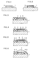
- Figure 1 is a sectional view showing an electrode structure for use in a silicon semiconductor device, which is an embodiment of the invention;
- Figure 2 is a sectional view showing an electrode structure for use in a silicon semiconductor device, which is another embodiment of the invention;
- Figure 3 is a sectional view showing the electrode of the semiconductor device of Figure 1 shielded by insulating material;
- Figure 4 is a sectional view showing a window opened in the insulating material shielding the electrode in Figure 3 and adhesiveness imparted to the exposed portion;
- Figure 5 is a sectional view showing solder powder supplied to the window portion in Figure 4;
- Figure 6 is a sectional view showing a solder bump formed by heating and melting the solder powder at the window portion;
- Figure 7 is a sectional view showing a device formed with solder bumps mountable on a wiring board;
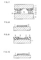
- Figure 8 is a sectional view showing a first embodiment of an electrode structure formed on a semiconductor chip;
- Figure 9 is a sectional view showing a second embodiment of an electrode structure formed on a semiconductor chip; and
- Figure 10 is a sectional view showing a conventional electrode structure formed on a semiconductor chip.
-
- The electrode structure embodying the invention for use in a silicon semiconductor device will be described first in detail with reference to the accompanying drawings.
- As shown in Figure 1, the electrode structure is provided on the silicon substrate surface of a
silicon semiconductor device 1 by using vacuum evaporation, sputtering or the like to form afirst metal layer 2 to a prescribed thickness and then forming asecond metal layer 3 to a prescribed thickness so as to cover thefirst metal layer 2 completely (including its side surfaces). Although not shown in the drawings, functional layer portions are present in the silicon semiconductor and electrodes are provided at a prescribed pitch to be positioned at the respective functional layer portions. - The metal used for the
first metal layer 2 of the electrode structure is selected from among metals that make ohmic contact with thesilicon substrate 1. Metals that make ohmic contact with silicon include Al, Cu, Ti, W and Al-base alloys. The Al-base alloys include Al-Si, Al-Ti and Al-W alloys containing not more than 5%, preferably 1-3%, of Si, Ti and W. After thefirst metal layer 2 has been formed of one of these metals on the silicon semiconductor device, heat treatment is effected to establish ohmic contact. Al-base alloys have coefficients of thermal expansion near that of silicon. Use of such an alloy is therefore advantageous from the point of alleviating strain at the metal-silicon interface. - The metal of the
second metal layer 3 to be formed on thefirst metal layer 2 is required to have higher resistance to corrosion by organic acid and better solder wettability than the metal of thefirst metal layer 2 and to exhibit good contact property with both the silicon semiconductor and the first metal layer. Specific examples include Cu, Ni and Au. When the first metal layer is made of Cu, a different metal (metal other than Cu) is selected for the second metal layer. The selection of the metal of the second metal layer is preferably made taking into account compatibility with the solder used to mount thesilicon semiconductor device 1 on a wiring board and the contact property between the silicon semiconductor and the first metal layer. - The
second metal layer 3 is formed by vacuum evaporation, sputtering, plating or the like to completely cover thefirst metal layer 2 and constitute an electrode. - Although, as just explained, the electrode formed on the
semiconductor 1 is composed of thefirst metal layer 2 and thesecond metal layer 3, preferably, as shown in Figure 2, it further includes between the first and second metal layers an intermediate metal layer 4 of Ni or Cr (limited to Cr if the second metal layer is made of Ni). The intermediate metal layer 4 is overlaid to completely cover thefirst metal layer 2 and thesecond metal layer 3 is overlaid to completely cover the intermediate metal layer 4. The intermediate metal layer 4 enhances the strength of thesecond metal layer 3 serving as the surface electrode. - There will next be explained a solder-bearing silicon semiconductor device obtained by forming a solder layer of a thickness of 50-100µm or greater (a "solder bump") on a silicon semiconductor device provided with the electrode of the foregoing structure. After an electrode has been formed on a surface of the
silicon semiconductor 1 as shown in Figures 1 and 2, the surface of the semiconductor is covered with aninsulating material 5 such as SiO2, Si3N4, glass, polyimide or the like by use of a conventional method such as vacuum evaporation, CVD or the like. The result is shown in Figure 3. The portion of the insulating material over the electrode is then removed by an ordinary method or by use of a mask to open a window as shown in Figure 4. Only the exposed portion of the second metal layer at this window is selectively imparted with anadhesive substance 6. Solder powder is then sprinkled to the window portion to adhere a layer ofsolder powder 7 to the formedadhesive portion 6 as shown in Figure 5. Next, thesolder powder 7 is melted by heating to form asolder bump 8 in the window as shown in Figure 6. - A particular feature of this invention is that the solder bump is formed to a considerable thickness of 50-100µm or even greater. To form such a solder bump, the semiconductor device having the
first metal layer 2 covered by thesecond metal layer 3 is covered by resist (the insulating material) in the foregoing manner, the metal electrode (the second metal layer) is exposed by etching in the foregoing manner, the exposed metal portion is selectively imparted with adhesiveness, solder powder is adhered to the adhesive portion, and the solder bump is formed by melting the solder powder. In this case it suffices for the resist forming the window to have a thickness of around 10µm. - The height of the solder bump can be adjusted by appropriately selecting the particle size of the solder powder supplied to the window.
- Impartation of adhesiveness to the exposed metal portion is effected by soaking in or coating with an aqueous solution containing at least one member among napthotriazole derivative, benzotriazole derivative, imidazole derivative, benzoimidazole derivative, mercaptobenzothiazole derivative, and benzothiazole thiofatty acid derivative. (See U.S. Patent Nos. 5,556,023 and 5,713,997.)
- This treatment is effected under conditions of, for example, a temperature of 30-60°C and a soaking period of 5sec-5min. The aqueous solution is prepared to contain at least one of napthotriazole derivative, benzotriazole derivative, imidazole derivative, benzoimidazole derivative, mercaptobenzothiazole derivative, and benzothiazole thiofatty acid derivative at a concentration of 0.05-20wt%. In particular, it is preferable to use as the solution for imparting solder adhesiveness one that is a slightly acidic liquid containing 50-1000ppm of copper ion.
- Although this solution for imparting adhesiveness is relatively stable, it exhibits strong corrosivity to the Al etc. forming the first metal layer and is highly likely to side-etch an electrode of such a metal. In addition, for reasons not yet determined, it results in a high defective product ratio even when side etching does not occur owing to incomplete coverage. The first metal layer must therefore be completely covered by the second metal layer as explained in the foregoing.
- The foregoing method of shielding one surface of the semiconductor device throughout with insulating material, forming a window (usually multiple windows) in the insulating material, selectively imparting adhesiveness to the portion at the window and adhering solder powder to this portion provides as advantageous features that no troublesome positioning steps or the like are required and that the adhesion of the solder powder can be easily automated. Moreover, unlike the conventional plating method and the like, which encounter difficulty in forming a solder layer of great thickness, the method of the invention enables a thick solder layer to be formed with ease because, even if the required thickness cannot be secured by a single cycle of the processing steps, the object can be achieved by once heating the semiconductor device adhered with the solder layer to melt part of the crown of the solder layer and then repeating the steps of the cycle to impart adhesiveness to the solder-coated portion, selectively adhere solder powder to the portion imparted with adhesiveness, and melt the adhered solder powder by heating. In addition to providing a thick layer by a single processing cycle, this method enables a still thicker solder layer to be obtained simply by adhering another solder layer to an earlier formed solder layer.
- The method of forming a solder bump on a semiconductor device explained in the foregoing can also be applied, as shown in Figure 7, to form a solder bump 13 (usually multiple solder bumps 13 as in the illustrated case) on a
wiring board 13. Specifically, thewiring board 11 is coated with resist, only the bonding portions 12 (electrode portions) of thewiring board 11 are exposed, adhesiveness is imparted to the exposed portions, solder powder is supplied to the adhesive portions and the solder powder is melted by heating to form the solder bumps 13. The solder bumps 8 and 13 of thesemiconductor device 1 and thewiring board 11 are then brought into contact so as to partially fuse, whereby the semiconductor device can be mounted at a large bonding height (gap) 14. Thegap 14 between the device and the wiring board of the circuit board obtained by mounting the semiconductor device in the foregoing manner can, if found necessary or desirable, be charged with insulating resin for sealing. - When a circuit board having a bonding height of 50-100µm is to be fabricated, the bump height on the semiconductor device side (electrode height + solder bump height) is made 50-120µm and the bump height on the wiring board side (electrode height + bump height) is made 30-100µm so that the desired bonding height can be obtained without fail even after the bumps are bonded by melting a portion of their solder.
- The compositions of the solder powders for the semiconductor device and wiring board sides can be made slightly different to give them different melting points. In this case, alloying of the higher melting point solder bump with the lower melting point solder bump starts before the higher melting point solder bump melts. This is advantageous because it helps to preserve the shape of the bumps and, by this, to maintain the desired bonding height.
- This effect can be obtained, for example, by on the semiconductor device side using 80Pb/20Sn, 95Pb/5Sn or other solder with a higher melting point than Sn-Pb eutectic solder and on the wiring board side using Sn-Pb eutectic solder.
- The solder-bearing silicon semiconductor device according to the invention can thus be mounted without use of bonding wires. A semiconductor device bonded by bonding wire requires resin to be molded on stems or the like for protecting the bonding wire, which becomes considerably larger than the semiconductor device chip itself and takes up a large area on the circuit board. Since the semiconductor device of the invention does not require use of bonding wire, it makes a highly effective and advantageous contribution to size reduction.
- The fact that a metal with good solder wettability is selected for the second metal layer makes mounting easy and ensures reliable bonding. In particular, the bonding by solder to solder provides highly conductive, strong bonding that enables direct mounting of the semiconductor device on the wiring board and greatly enhances bonding reliability.
- Owing to the relative freedom in selecting the bonding height, the circuit board of the invention can be fabricated to have high tolerance and high height. Because of this, the invention circuit board can avoid the heat problems encountered in the past even when fabricated using identical materials and the same kind of semiconductor device. This also facilitates circuit board design.
- Examples of the invention will now be explained. The invention is, however, not limited to the specific embodiments described.
- Sixteen
first metal layers 2 each composed of Al measuring 90µm in diameter and 1µm in thickness were formed on a 5-mmsquare silicon chip 1 at a pitch of 250µm by vacuum evaporation.Second metal layers 3 consisting of Cu were formed by vacuum evaporation to a thickness of 1µm on the Alfirst metal layers 2 so as to cover all surfaces thereof including the side surfaces. By this there were obtained 16 electrodes of the structure shown in Figure 8 (electrode structure I). - Separately, 16
first metal layers 2 were formed on asilicon chip 1 by vacuum evaporation in the same manner as just described except that Cu was used instead of Al.Second metal layers 3 consisting of Ni were formed by vacuum evaporation to a thickness of 3µm on the Cufirst metal layers 2 so as to cover all surfaces thereof including the side surfaces. By this there were obtained 16 electrodes of the structure shown in Figure 8 (electrode structure II). - Further, 16
first metal layers 2 were formed on asilicon chip 1 by vacuum evaporation in the same manner except that Al-2%Si alloy was used instead of Al.Second metal layers 3 consisting of Cu were formed by vacuum evaporation to a thickness of 1µm on the Al-Si alloyfirst metal layers 2 so as to cover all surfaces thereof including the side surfaces. By this there were obtained 16 electrodes of the structure shown in Figure 8 (electrode structure III). - Further, 16
first metal layers 2 each composed of Al measuring 90µm in diameter and 1µm in thickness were formed on a 5-mmsquare silicon chip 1 at a pitch of 250µm by vacuum evaporation.Second metal layers 3 consisting of Cu were formed by vacuum evaporation to a thickness of 1µm on the Alfirst metal layers 2 so as to cover all surfaces thereof including the side surfaces. ASiO2 layer 5 was then formed to a thickness of 10µm throughout as a shield, whereafter it was etched at prescribed locations to form windows and expose the Cu electrode surfaces. By this there were obtained 16 electrodes of the structure shown in Figure 9 (electrode structure IV). - As a comparative example, 16
first metal layers 2 each composed of Al measuring 90µm in diameter and 1µm in thickness were formed on a 5-mmsquare silicon chip 1 at a pitch of 250µm by vacuum evaporation.Second metal layers 3 consisting of Cu were formed by vacuum evaporation to a thickness of 1µm on the Alfirst metal layers 2 so as to cover only their upper surfaces. By this there were obtained 16 electrodes of the structure shown in Figure 10 (electrode structure V). - This comparative example was repeated except that the 16
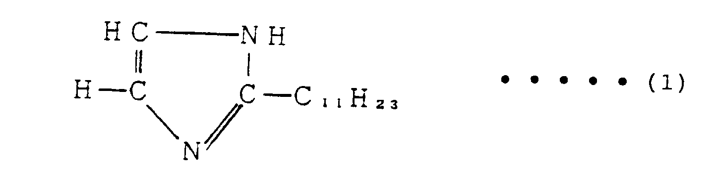
first metal layers 2 were formed by vacuum evaporation using Cu instead of Al and thesecond metal layers 3 were formed of Ni to a thickness of 3µm by vacuum evaporation so as to cover only the top surfaces of the Cu first metal layers 2. By this there were obtained 16 electrodes of the structure shown in Figure 10 (electrode structure VI). - The aforesaid six silicon chips provided with electrodes were pretreated with aqueous solution of sulfuric acid and were then soaked for 5min in a 40°C adhesiveness imparting solution composed of a 2wt% aqueous solution of 2-undecylimidazole (formula (1) shown below) adjusted to pH of approximately 4.5 with acetic acid.
- The six silicon chips were removed from the solution, washed with water and dried. Next, 20Sn/80Pb solder powder of an average particle size of 120µm was sprinkled over the whole surface of the silicon chips formed with the electrodes. Excess powder at regions other than the electrodes was blown off with air. The condition of powder adhesion at this time is summarized in Table 1.
Sample Adhesion Remark Electrode structure (1) Good Adhesion good throughout Electrode structure (2) Good Adhesion good throughout Electrode structure (3) Good Adhesion good throughout Electrode structure (4) Good Adhesion good throughout Comparative examples Electrode structure (5) Poor Adhesion impaired by generation of extraneous matter Electrode structure (6) Fair Adherence at only a portion of electrode - The six silicon chips adhered with solder powder were heated for 30sec in a stream of 170°C nitrogen gas to fix the solder powder, coated with water-soluble flux, preheated to 150°C in a reflow furnace passing nitrogen gas containing 500ppm of oxygen and heated to a reflow temperature of 300°C to melt the solder powder. They were then cleaned with hot water. The state of solder bump formation was examined and the bump height and bump height standard deviation (σ) were measured. The results are shown in Table 2. As is clear from this table, the heights of solder bumps are uniform. Therefore, the chips having the electrode structures I to IV will be able to be all stably mounted on a wiring board.
Sample Shape of solder bumps Remark Solder bump height (µm ) Standard deviation (σ) Electrode structure (I) Good Good coating 103 3.0 Electrode structure (II) Good Good coating 105 3.1 Electrode structure (III) Good Good coating 105 3.1 Electrode structure (IV) Good Good coating 102 3.0 Comparative examples Electrode structure (V) Poor No coating - - -- Electrode structure (VI) Fair Some coating missing - - -- - Sixteen
first metal layers 2 each composed of Al measuring 90µm in diameter and 1µm in thickness were formed on a 5-mm squaresilicon device substrate 1 at a pitch of 250µm by vacuum evaporation.Second metal layers 3 consisting of Cu were formed by vacuum evaporation to a thickness of 1µm on the Alfirst metal layers 2 so as to cover all surfaces thereof including the side surfaces. By this there were obtained 16 electrodes of the structure shown in Figure 8. Thissilicon device substrate 1 provided with electrodes was pretreated with aqueous solution of sulfuric acid and then soaked for 5min in a 40°C adhesiveness imparting solution composed of a 2wt% aqueous solution of 2-undecylimidazole adjusted to pH of approximately 4.5 with acetic acid. - The substrate was removed from the solution, washed with water, dried and sprinkled with 20Sn/80Pb solder powder. Excess powder was blown off with air.
- The silicon device substrate adhered with solder powder in this manner was heated for 30sec in a stream of 170°C nitrogen gas to fix the solder powder, coated on the solder with water-soluble flux, preheated to 150°C in a reflow furnace passing nitrogen gas containing 500ppm of oxygen and heated to a reflow temperature of 300°C to melt the solder powder. It was then cleaned with hot water to obtain a solder-bearing silicon semiconductor device having approximately 60µm high solder bumps.
- The foregoing process was repeated except for sprinkling solder powders of different grain sizes to obtain solder-bearing silicon semiconductor devices having solder bumps with heights measuring 80µm, 100µm and 120µm instead of 60µm.
- Next, the copper circuits of a printed wiring board having 16 copper plated circuits of 90µm width and 250µm pitch were exposed over 90µm x 90µm at prescribed locations and the remaining portions were coated with resist resin. As in the case of the silicon device, the board was acid-cleaned with aqueous solution of sulfuric acid and then soaked in an adhesiveness imparting solution adjusted to pH of approximately 4.5 with acetic acid to impart adhesiveness to the exposed copper circuit portions.
- The printed wiring board was then sprinkled with Sn/37Pb eutectic solder powder and excess powder was blown off with air. It was next heat treated to form an approximately 30µm high solder bump at each copper circuit.
- The foregoing process was repeated except for sprinkling solder powders of different particle sizes to obtain wiring boards having solder bumps with heights measuring 60µm, 80µm and 100µm instead of 30µm.
- The solder-bearing silicon devices and the wiring boards provided with solder bumps in the foregoing manner were coated on their solder bumps with flux, placed with their solder bumps in contact, preheated to 150°C in a reflow furnace passing nitrogen gas containing 500ppm of oxygen and heated to a reflow temperature of 200°C to melt and bond the tip portions of the solder, thereby obtaining circuit boards having silicon semiconductor devices mounted thereon (see Figure 7).
- The bonding heights obtained with devices and circuit boards having solder bumps of different heights are shown in Table 3.
- As is clear from this table, circuit boards having bonding heights in the range of 40-87µm can be easily obtained by selecting the combination of device and wiring board used.
Bump height (Silicon device) (µm) Bump height (Wiring board) (µm) Bonding height (µm) 60 30 40 80 30 56 100 30 69 120 30 87 60 60 55 60 80 64 60 100 77 - As is clear from the foregoing, the silicon semiconductor device according to the invention is excellent in solder contact property owing to its good resistance to solder corrosion and good solder wettability. When the intermediate metal layer is introduced between the first metal layer and the second metal layer, moreover, the strength of the surface electrode is enhanced. In addition, since the intermediate metal layer and the second metal layer each completely covers the layer thereunder, the metal of the lower layer is safe from being eaten away by solder or being side etched by the chemical for imparting adhesiveness.
- Another merit is that the solder bump height can be easily controlled by selecting the particle size of the solder powder adhered in the solder powder adhering step. When this solder-bearing silicon semiconductor device is mounted on a wiring board, the mounting is effected after the wiring board has also been formed with similar solder bumps. Since this enables securement of a large bonding height, it provides higher heat resistance property and greater ease of circuit board design for a given combination of material and semiconductor device.
- Since the invention thus enables semiconductor device mounting without use of bonding wire, it achieves low bonding resistance and high bonding strength while enjoying the superb reliability of solder-to-solder bonding.
Claims (26)
- An electrode structure for a silicon semiconductor device comprising two metal layers provided on a semiconductor surface (1) of the semiconductor device, characterised in that a first metal layer (2) of the two metal layers makes ohmic contact with the semiconductor, that a second metal layer (3) is overlaid on the first metal layer to completely cover all surfaces including side surfaces thereof, and that the metal of the second metal layer has higher resistance to corrosion by organic acid and better solder wettability than the metal of the first metal layer (2).
- An electrode structure according to claim 1, characterised in that the metal of the first metal layer (2) is one member selected from among Cu, Al, Ti, W and Al-base alloy and that the metal of the second metal layer (3) is one member selected from among Cu, Ni and Au but excluding Cu when the first metal layer is of Cu.
- An electrode structure according to any one of claims 1 and 2, characterised in that it further has an intermediate metal layer (4) of Ni or Cr interposed between the first metal layer (2) and the second metal layer (3) to completely cover the first metal layer, provided that the intermediate layer is limited to Cr when the second metal layer is of Ni, and that the second metal layer completely covers the intermediate layer.
- An electrode structure according to claim 2, characterised in that the Al-base alloy is one member selected from among Al-Si, Al-Ti and Al-W containing not more than 5% of Si, Ti or W.
- An electrode structure according to claim 1, characterised in that all but a prescribed region of the surface of the second metal layer (3) is shielded by an insulating material (5).
- An electrode structure according to claim 5, characterised in that the insulating material (5) is one member selected from among SiO2, Si3N4, glass and polyimide resin.
- A solder-bearing silicon semiconductor device having a solder-bearing electrode provided thereon, characterised in that the electrode comprises a first metal layer (2) provided on a surface of the semiconductor (1) to make ohmic contact with the semiconductor device and a second metal layer (3) overlaid on the first metal layer to completely cover all surfaces including side surfaces thereof, that the metal of the second metal layer has higher resistance to corrosion by organic acid and better solder wettability than the metal of the first metal layer, and that the surface of the second metal layer is provided with a solder bump (8) seated on a prescribed region thereof.
- A semiconductor device according to claim 7, characterised in that the metal of the first metal layer (2) is one member selected from among Cu, Al, Ti, W and Al-base alloy and that the metal of the second metal layer (3) is one member selected from among Cu, Ni and Au but excluding Cu when the first metal layer is of Cu.
- A semiconductor device according to any one of claims 7 and 8, characterised in that it further has an intermediate metal layer (4) of Ni or Cr interposed between the first metal layer (2) and the second metal layer (3) to completely cover the first metal layer, provided that the intermediate layer is limited to Cr when the second metal layer is of Ni, and that the second metal layer completely covers the intermediate layer.
- A semiconductor device according to claim 8, characterised in that the Al-base alloy is one member selected from among Al-Si, Al-Ti and Al-W containing not more than 5% of Si, Ti or W.
- A semiconductor device according to claim 7, characterised in that the solder bump (8) seated on the prescribed region of the surface of the second metal layer (3) is shielded by an insulating material (5).
- A semiconductor device according to claim 7, characterised in that the insulating material (5) is one member selected from among SiO2, Si3N4, glass and polyimide resin.
- A method of fabricating a solder-bearing silicon semiconductor device having a solder-bearing electrode provided thereon, characterised byforming on a silicon semiconductor device (1) a first metal layer (2) that makes ohmic contact with the semiconductor device,overlaying a second metal layer (3) on the first metal layer to completely cover all surfaces including side surfaces thereof, the metal of the second metal layer having higher resistance to corrosion by organic acid and better solder wettability than the metal of the first metal layer,covering the whole surface of the second metal layer with an insulating material (5),etching the insulating material to open a window exposing a prescribed region of the surface of the second metal layer,selectively imparting adhesiveness (6) to the exposed surface of the second metal layer,adhering solder powder (7) to the adhesive portion imparted with adhesiveness, andmelting the adhered solder powder by heating to form a solder bump (8) on the surface of the second metal layer.
- A fabricating method according to claim 13, characterised in that the metal of the first metal layer (2) is one member selected from among Cu, Al, Ti, W and Al-base alloy and that the metal of the second metal layer (3) is one member selected from among Cu, Ni and Au but excluding Cu when the first metal layer is of Cu.
- A fabricating method according to claim 14, characterised in that the Al-base alloy is one member selected from among Al-Si, Al-Ti and Al-W containing not more than 5% of Si, Ti or W.
- A fabricating method according to claim 13, characterised in that the insulating material (5) is one member selected from among SiO2, Si3N4, glass and polyimide resin.
- A circuit board mounted with a semiconductor device comprising a wiring board (11) and a silicon semiconductor device (1), characterised in that the semiconductor device (1) has electrodes (2, 3) provided thereon, the surfaces of which are imparted with adhesiveness (6), and solder powder (7) adhering to the adhesive surfaces of the electrodes and melted by heating to form a solder bump (8), that the wiring board (11) has an electrode portion (12) imparted with adhesiveness and solder powder adhering to the adhesive electrode portion and melted by heating to form a solder bump (13), and that the semiconductor device (1) and the wiring board (11) are adhered together through fusion of the solder bumps (8, 13).
- A circuit board according to claim 17, characterised in that the electrodes (2, 3) comprises a first metal layer (2) that makes ohmic contact with the semiconductor device (1) and a second metal layer (3) overlaid on the first metal layer to completely cover all surfaces including side surfaces thereof and that the metal of the second metal layer has higher resistance to corrosion by organic acid and better solder wettability than the metal of the first metal layer.
- A circuit board according to claim 18, characterised in that the metal of the first metal layer (2) is one member selected from among Cu, Al, Ti, W and Al-base alloy and that the metal of the second metal layer (3) is one member selected from among Cu, Ni and Au but excluding Cu when the first metal layer is of Cu.
- A circuit board according to claim 19, characterised in that the Al-base alloy is one member selected from among Al-Si, Al-Ti and Al-W containing not more than 5% of Si, Ti or W.
- A method of fabricating a circuit board mounted with a semiconductor device, characterised byforming on a silicon semiconductor device (1) a first metal layer (2) that makes ohmic contact with the semiconductor device,overlaying a second metal layer (3) on the first metal layer to completely cover all surfaces including side surfaces thereof, the metal of the second metal layer having higher resistance to corrosion by organic acid and better solder wettability than the metal of the first metal layer,covering the whole surface of the second metal layer with an insulating material (5),etching the insulating material to open a window exposing a prescribed region of the surface of the second metal layer,selectively imparting adhesiveness (6) to the exposed surface of the second metal layer,adhering solder powder (7) to the adhesive portion imparted with adhesiveness,melting the adhered solder powder by heating to form a solder bump (8) on the surface of the second metal layer,selectively imparting adhesiveness to an electrode portion (12) of a wiring board (11),adhering solder powder to the adhesive electrode portion of the wiring board imparted with adhesiveness,melting the adhered solder powder by heating to form a solder bump (13) on the electrode portion, andcontacting and fusing the solder bump of the semiconductor device and the solder bump of the wiring board so as to form a prescribed gap portion (14).
- A fabricating method according to claim 21, characterised in that the metal of the first metal layer (2) is one member selected from among Cu, Al, Ti, W and Al-base alloy and that the metal of the second metal layer (3) is one member selected from among Cu, Ni and Au but excluding Cu when the first metal layer is of Cu.
- A fabricating method according to claim 22, characterised in that the Al-base alloy is one member selected from among Al-Si, Al-Ti and Al-W containing not more than 5% of Si, Ti or W.
- A fabricating method according to claim 21, characterised in that the insulating material (5) is one member selected from among SiO2, Si3N4, glass and polyimide resin.
- A fabricating method according to claim 21, characterised in that the solder powder imparted to the adhesive portion of the second metal layer and the solder powder imparted to the adhesive electrode portion of the wiring board have different melting points.
- A fabricating method according to claim 21, characterised in that it further comprises charging insulating resin for sealing into the gap portion (14) between the semiconductor device and the wiring board.
Applications Claiming Priority (3)
| Application Number | Priority Date | Filing Date | Title |
|---|---|---|---|
| JP24339797 | 1997-08-25 | ||
| JP24339797 | 1997-08-25 | ||
| JP243397/97 | 1997-08-25 |
Publications (3)
| Publication Number | Publication Date |
|---|---|
| EP0899786A2 true EP0899786A2 (en) | 1999-03-03 |
| EP0899786A3 EP0899786A3 (en) | 2000-01-19 |
| EP0899786B1 EP0899786B1 (en) | 2003-04-23 |
Family
ID=17103265
Family Applications (1)
| Application Number | Title | Priority Date | Filing Date |
|---|---|---|---|
| EP98306749A Expired - Lifetime EP0899786B1 (en) | 1997-08-25 | 1998-08-24 | Electrode structure of a silicon semiconductor device |
Country Status (5)
| Country | Link |
|---|---|
| US (2) | US5982629A (en) |
| EP (1) | EP0899786B1 (en) |
| KR (1) | KR100300462B1 (en) |
| DE (1) | DE69813701T2 (en) |
| TW (1) | TW453137B (en) |
Cited By (1)
| Publication number | Priority date | Publication date | Assignee | Title |
|---|---|---|---|---|
| US7422973B2 (en) * | 2006-01-27 | 2008-09-09 | Freescale Semiconductor, Inc. | Method for forming multi-layer bumps on a substrate |
Families Citing this family (24)
| Publication number | Priority date | Publication date | Assignee | Title |
|---|---|---|---|---|
| JP3268386B2 (en) * | 1998-06-29 | 2002-03-25 | 日本航空電子工業株式会社 | Method of forming corrosion prevention film |
| JP3678048B2 (en) * | 1999-04-05 | 2005-08-03 | 松下電器産業株式会社 | Solder precoat method and solder precoat substrate |
| US6402012B1 (en) * | 1999-11-08 | 2002-06-11 | Delphi Technologies, Inc. | Method for forming solder bumps using a solder jetting device |
| SG99331A1 (en) | 2000-01-13 | 2003-10-27 | Hitachi Ltd | Method of producing electronic part with bumps and method of producing elctronic part |
| JP3952434B2 (en) * | 2000-03-29 | 2007-08-01 | ローム株式会社 | Battery pack and manufacturing method thereof |
| WO2001078931A1 (en) * | 2000-04-17 | 2001-10-25 | Fujitsu Limited | Solder joining |
| JP3968554B2 (en) * | 2000-05-01 | 2007-08-29 | セイコーエプソン株式会社 | Bump forming method and semiconductor device manufacturing method |
| JP3687610B2 (en) * | 2002-01-18 | 2005-08-24 | セイコーエプソン株式会社 | Semiconductor device, circuit board, and electronic equipment |
| US6653236B2 (en) * | 2002-03-29 | 2003-11-25 | Micron Technology, Inc. | Methods of forming metal-containing films over surfaces of semiconductor substrates; and semiconductor constructions |
| US7341947B2 (en) * | 2002-03-29 | 2008-03-11 | Micron Technology, Inc. | Methods of forming metal-containing films over surfaces of semiconductor substrates |
| JP3565835B1 (en) * | 2003-04-28 | 2004-09-15 | 松下電器産業株式会社 | Wiring board, method of manufacturing the same, semiconductor device and method of manufacturing the same |
| JP2006032446A (en) * | 2004-07-13 | 2006-02-02 | Toshiba Corp | Mounting method for semiconductor component, and mounting device |
| US7897452B2 (en) * | 2005-06-20 | 2011-03-01 | Fuji Electric Systems Co., Ltd. | Method of producing a semiconductor device with an aluminum or aluminum alloy rear electrode |
| TW200713472A (en) * | 2005-09-19 | 2007-04-01 | Analog Integrations Corp | Polymer material and local connection structure of chip |
| JP4839138B2 (en) * | 2006-06-20 | 2011-12-21 | 新光電気工業株式会社 | Wiring board manufacturing method |
| US7600667B2 (en) * | 2006-09-29 | 2009-10-13 | Intel Corporation | Method of assembling carbon nanotube reinforced solder caps |
| US20080079175A1 (en) * | 2006-10-02 | 2008-04-03 | Michael Bauer | Layer for chip contact element |
| US8264072B2 (en) * | 2007-10-22 | 2012-09-11 | Infineon Technologies Ag | Electronic device |
| US20100032194A1 (en) * | 2008-08-08 | 2010-02-11 | Ibiden Co., Ltd. | Printed wiring board, manufacturing method for printed wiring board and electronic device |
| JP5456545B2 (en) * | 2009-04-28 | 2014-04-02 | 昭和電工株式会社 | Circuit board manufacturing method |
| US8378485B2 (en) * | 2009-07-13 | 2013-02-19 | Lsi Corporation | Solder interconnect by addition of copper |
| EP3273755B1 (en) * | 2009-09-15 | 2018-11-07 | Kabushiki Kaisha Toshiba | Process for producing a ceramic circuit board |
| US9330993B2 (en) * | 2012-12-20 | 2016-05-03 | Intel Corporation | Methods of promoting adhesion between underfill and conductive bumps and structures formed thereby |
| US10695875B2 (en) * | 2018-03-19 | 2020-06-30 | Asia Vital Components Co., Ltd. | Soldering method of soldering jig |
Citations (4)
| Publication number | Priority date | Publication date | Assignee | Title |
|---|---|---|---|---|
| EP0354114A1 (en) * | 1988-08-02 | 1990-02-07 | Mcnc | Method of building solder bumps and resulting structure |
| EP0357064A2 (en) * | 1988-09-02 | 1990-03-07 | Kabushiki Kaisha Toshiba | Metal bump type semiconductor device and method for manufacturing the same |
| EP0595343A2 (en) * | 1992-10-30 | 1994-05-04 | Showa Denko Kabushiki Kaisha | Method of forming solder film |
| US5586715A (en) * | 1994-08-08 | 1996-12-24 | Hewlett-Packard Company | Method of making solder balls by contained paste deposition |
Family Cites Families (13)
| Publication number | Priority date | Publication date | Assignee | Title |
|---|---|---|---|---|
| DE2032872B2 (en) * | 1970-07-02 | 1975-03-20 | Siemens Ag, 1000 Berlin Und 8000 Muenchen | Process for the production of soft solderable contacts for the installation of semiconductor components in housings |
| US4505029A (en) * | 1981-03-23 | 1985-03-19 | General Electric Company | Semiconductor device with built-up low resistance contact |
| US5272376A (en) * | 1990-06-01 | 1993-12-21 | Clarion Co., Ltd. | Electrode structure for a semiconductor device |
| JP3141364B2 (en) * | 1992-05-06 | 2001-03-05 | 住友電気工業株式会社 | Semiconductor chip |
| US5556023A (en) * | 1992-10-30 | 1996-09-17 | Showa Denko K.K. | Method of forming solder film |
| JP3361881B2 (en) * | 1994-04-28 | 2003-01-07 | 株式会社東芝 | Semiconductor device and manufacturing method thereof |
| JP3238011B2 (en) * | 1994-07-27 | 2001-12-10 | 株式会社東芝 | Semiconductor device |
| US5601459A (en) * | 1994-09-29 | 1997-02-11 | North American Specialties Corporation | Solder bearing lead and method of fabrication |
| US5656858A (en) * | 1994-10-19 | 1997-08-12 | Nippondenso Co., Ltd. | Semiconductor device with bump structure |
| JP3217624B2 (en) * | 1994-11-12 | 2001-10-09 | 東芝マイクロエレクトロニクス株式会社 | Semiconductor device |
| KR100349896B1 (en) * | 1994-12-28 | 2002-12-26 | 삼성에스디아이 주식회사 | Mounting structure of ic and mounting method thereof |
| US5889326A (en) * | 1996-02-27 | 1999-03-30 | Nec Corporation | Structure for bonding semiconductor device to substrate |
| KR100216839B1 (en) * | 1996-04-01 | 1999-09-01 | 김규현 | Solder ball land structure of bga semiconductor package |
-
1998
- 1998-06-25 TW TW087110259A patent/TW453137B/en not_active IP Right Cessation
- 1998-07-09 KR KR1019980027609A patent/KR100300462B1/en not_active IP Right Cessation
- 1998-08-24 EP EP98306749A patent/EP0899786B1/en not_active Expired - Lifetime
- 1998-08-24 DE DE69813701T patent/DE69813701T2/en not_active Expired - Lifetime
- 1998-08-25 US US09/139,562 patent/US5982629A/en not_active Expired - Lifetime
-
1999
- 1999-08-25 US US09/382,673 patent/US6221692B1/en not_active Expired - Lifetime
Patent Citations (4)
| Publication number | Priority date | Publication date | Assignee | Title |
|---|---|---|---|---|
| EP0354114A1 (en) * | 1988-08-02 | 1990-02-07 | Mcnc | Method of building solder bumps and resulting structure |
| EP0357064A2 (en) * | 1988-09-02 | 1990-03-07 | Kabushiki Kaisha Toshiba | Metal bump type semiconductor device and method for manufacturing the same |
| EP0595343A2 (en) * | 1992-10-30 | 1994-05-04 | Showa Denko Kabushiki Kaisha | Method of forming solder film |
| US5586715A (en) * | 1994-08-08 | 1996-12-24 | Hewlett-Packard Company | Method of making solder balls by contained paste deposition |
Cited By (1)
| Publication number | Priority date | Publication date | Assignee | Title |
|---|---|---|---|---|
| US7422973B2 (en) * | 2006-01-27 | 2008-09-09 | Freescale Semiconductor, Inc. | Method for forming multi-layer bumps on a substrate |
Also Published As
| Publication number | Publication date |
|---|---|
| US5982629A (en) | 1999-11-09 |
| DE69813701D1 (en) | 2003-05-28 |
| DE69813701T2 (en) | 2004-03-11 |
| KR100300462B1 (en) | 2001-10-19 |
| EP0899786B1 (en) | 2003-04-23 |
| US6221692B1 (en) | 2001-04-24 |
| KR19990023187A (en) | 1999-03-25 |
| TW453137B (en) | 2001-09-01 |
| EP0899786A3 (en) | 2000-01-19 |
Similar Documents
| Publication | Publication Date | Title |
|---|---|---|
| EP0899786B1 (en) | Electrode structure of a silicon semiconductor device | |
| US5329158A (en) | Surface mountable semiconductor device having self loaded solder joints | |
| US6307160B1 (en) | High-strength solder interconnect for copper/electroless nickel/immersion gold metallization solder pad and method | |
| JP2807940B2 (en) | Adhesive having flux agent and metal particles | |
| JP2589239B2 (en) | Thermosetting adhesive and electrical component assembly using the same | |
| US6164523A (en) | Electronic component and method of manufacture | |
| TWI230104B (en) | Electronic device | |
| US20070020912A1 (en) | Semiconductor element and a producing method for the same, and a semiconductor device and a producing method for the same | |
| US6378758B1 (en) | Conductive leads with non-wettable surfaces | |
| JPH1197480A (en) | Interconnection structure with conductive adhesive | |
| JPH10509278A (en) | Flip-chip technology core metal solder knob | |
| WO1997047426A1 (en) | Lead-free, high tin ternary solder alloy of tin, silver, and indium | |
| JPH08164496A (en) | Sn-zn solder, sn-zn-bi solder, method for surface treatment of same, and mounted substrate using it | |
| US6548393B1 (en) | Semiconductor chip assembly with hardened connection joint | |
| JP3868766B2 (en) | Semiconductor device | |
| JP3356649B2 (en) | Semiconductor device and manufacturing method thereof | |
| US8071472B2 (en) | Semiconductor device with solder balls having high reliability | |
| US6271111B1 (en) | High density pluggable connector array and process thereof | |
| JP3339384B2 (en) | Solder material, printed wiring board and method of manufacturing the same | |
| JP3785822B2 (en) | ELECTRODE STRUCTURE, SILICON SEMICONDUCTOR ELEMENT HAVING THE ELECTRODE, MANUFACTURING METHOD THEREOF, CIRCUIT BOARD MOUNTING THE ELEMENT AND MANUFACTURING METHOD THEREOF | |
| JPH09148693A (en) | Flip chip mounting board and manufacture thereof | |
| US20020175424A1 (en) | Process of forming metal surfaces compatible with a wire bonding and semiconductor integrated circuits manufactured by the process | |
| JPH0732170B2 (en) | Semiconductor device | |
| JP3308060B2 (en) | Semiconductor device mounting method | |
| JP2911005B2 (en) | Processing method of bump electrode |
Legal Events
| Date | Code | Title | Description |
|---|---|---|---|
| PUAI | Public reference made under article 153(3) epc to a published international application that has entered the european phase |
Free format text: ORIGINAL CODE: 0009012 |
|
| AK | Designated contracting states |
Kind code of ref document: A2 Designated state(s): DE FR GB |
|
| AX | Request for extension of the european patent |
Free format text: AL;LT;LV;MK;RO;SI |
|
| PUAL | Search report despatched |
Free format text: ORIGINAL CODE: 0009013 |
|
| AK | Designated contracting states |
Kind code of ref document: A3 Designated state(s): AT BE CH CY DE DK ES FI FR GB GR IE IT LI LU MC NL PT SE |
|
| AX | Request for extension of the european patent |
Free format text: AL;LT;LV;MK;RO;SI |
|
| 17P | Request for examination filed |
Effective date: 20000717 |
|
| AKX | Designation fees paid |
Free format text: DE FR GB |
|
| 17Q | First examination report despatched |
Effective date: 20010514 |
|
| RTI1 | Title (correction) |
Free format text: ELECTRODE STRUCTURE OF A SILICON SEMICONDUCTOR DEVICE |
|
| GRAH | Despatch of communication of intention to grant a patent |
Free format text: ORIGINAL CODE: EPIDOS IGRA |
|
| GRAH | Despatch of communication of intention to grant a patent |
Free format text: ORIGINAL CODE: EPIDOS IGRA |
|
| GRAA | (expected) grant |
Free format text: ORIGINAL CODE: 0009210 |
|
| AK | Designated contracting states |
Designated state(s): DE FR GB |
|
| REG | Reference to a national code |
Ref country code: GB Ref legal event code: FG4D |
|
| REF | Corresponds to: |
Ref document number: 69813701 Country of ref document: DE Date of ref document: 20030528 Kind code of ref document: P |
|
| ET | Fr: translation filed | ||
| PLBE | No opposition filed within time limit |
Free format text: ORIGINAL CODE: 0009261 |
|
| STAA | Information on the status of an ep patent application or granted ep patent |
Free format text: STATUS: NO OPPOSITION FILED WITHIN TIME LIMIT |
|
| 26N | No opposition filed |
Effective date: 20040126 |
|
| PGFP | Annual fee paid to national office [announced via postgrant information from national office to epo] |
Ref country code: DE Payment date: 20110817 Year of fee payment: 14 Ref country code: FR Payment date: 20110818 Year of fee payment: 14 Ref country code: GB Payment date: 20110824 Year of fee payment: 14 |
|
| GBPC | Gb: european patent ceased through non-payment of renewal fee |
Effective date: 20120824 |
|
| REG | Reference to a national code |
Ref country code: FR Ref legal event code: ST Effective date: 20130430 |
|
| PG25 | Lapsed in a contracting state [announced via postgrant information from national office to epo] |
Ref country code: GB Free format text: LAPSE BECAUSE OF NON-PAYMENT OF DUE FEES Effective date: 20120824 Ref country code: DE Free format text: LAPSE BECAUSE OF NON-PAYMENT OF DUE FEES Effective date: 20130301 |
|
| PG25 | Lapsed in a contracting state [announced via postgrant information from national office to epo] |
Ref country code: FR Free format text: LAPSE BECAUSE OF NON-PAYMENT OF DUE FEES Effective date: 20120831 |
|
| REG | Reference to a national code |
Ref country code: DE Ref legal event code: R119 Ref document number: 69813701 Country of ref document: DE Effective date: 20130301 |