BACKGROUND OF THE INVENTION
The present invention relates to a single-chip
SONET physical layer device and, more particularly, to
a device which supports the ATM cell protocol and the
PPP protocol, while interfacing to common existing
components.
A Synchronous Optical NETwork (SONET) is an
optical signaling format defined for North America. The
international Synchronous Digital Hierarchy (SDH) is
closely related to the SONET signaling format, and the
term "SONET" will be used in the following specification
to refer to both SONET and SDH. A SONET STS-1 data
frame consists of 9 rows of 90 octets each, for a total
of 810 octets. An octet is unit of information
consisting of 8 digital bits. The term byte is
typically used interchangeably with the term octet. The
SONET STS-1 data frame is divided into two fields, a
section and line overhead field and a synchronous
payload envelope (SPE) field. The section and line
overhead field includes 27 octets. The SPE field
includes 783 octets of payload and 9 octets of path
overhead.
Current data packet transmissions over SONET
communication links are typically based upon the
Asynchronous Transfer Mode (ATM) cell protocol in which
ATM cells are placed into a SONET SPE and transmitted
over a SONET communications link. Alternative modes of
transmission are being defined using the point-to-point
protocol (PPP). A standard ATM cell consists of 53
octets, which includes a 5-octet header field and a 48-octet
payload field. The ATM cells "flow" along a
physical medium, such as an OC-3 optical fiber or a
similar carrier. The ATM cells are used for carrying
data, such as data files, between two networked PCs or
voice data (voice conversations) along multiple
telephone lines between two large telephone distribution
points. Since data files and digitized telephone
conversations are typically larger than the 48 octets
that would fit into the ATM cell payload field, it is
necessary to repackage the data in some form. The
device that performs the repackaging is referred to as
an ATM adaption layer (AAL). The AAL segments the data,
which is typically referred to as a protocol data unit
(PDU), into 48 octet-sized pieces that fit into the ATM
cell payload fields. Different types of AALs exist to
segment PDUs in different ways, with each type being
appropriate for a particular application. For example,
AAL1 is typically used for voice traffic while AAL5 is
typically used for file transfer and Ethernet traffic.
The PPP protocol is a High Level Data Link
Controller (HDLC) based protocol. The PPP protocol is
a popular and practical protocol for moving data traffic
between two computer systems. The most typical use of
the PPP protocol is for computer dial-up communication
with an Internet Service Provider (ISP) over telephone
lines. With a Windows®95 based personal computer, this
dial-up connection is typically a PPP connection, since
the PPP protocol support is built into Windows®95. The
PPP protocol consists of a data framing specification
and a management protocol. PPP can be implemented with
8-bit asynchronous links, bit-synchronous links or
octet-synchronous links. With octet-synchronous links,
all operations are based on complete octets and
individual bits are not operated on, nor inserted. A
PPP data frame of this type includes several fields,
including start flag, address, control, protocol,
payload, error correction and end flag fields. The
payload field typically consists of 0 to 1,500 octets.
Several transmission methodologies exist for
transmitting ATM and PPP over SONET communication links.
These methodologies include transmitting ATM cells in
SONET SPEs, transmitting PPP frames in ATM cells in
SONET SPEs, and transmitting PPP frames directly in
SONET SPEs. Transmitting ATM cells in SONET SPEs is a
current market norm. The data unit or frame to be
transmitted is segmented by an ATM adaption layer device
into multiple ATM cells and then transmitted to a SONET
physical layer device. The SONET physical layer device
receives the ATM cells and places them into the SONET
SPE for transmission over a SONET communications link.
A typical component for receiving ATM cells and placing
the cells in SONET SPEs is the S/UNI Lite available from
PMC-SIERRA, Inc.
Transmitting PPP frames in ATM cells in SONET
SPEs is a non-standard transmission mechanism. The data
unit to be transmitted is processed into a PPP frame
using a form of an HDLC processor in the octet-synchronous
mode. The resulting PPP frame is passed to
an ATM adaption layer device which segments the PPP
frame and places the segments into ATM cells, either in
a standard manner or in a non-standard manner by placing
the segments into both the cell payload field and the
cell header field (excluding an HEC byte). The later is
a more typical approach as it increases utilization of
the link. The resulting cells are passed to a SONET
physical layer device and placed into a SONET SPE. All
header processing is disabled. The S/UNI part can
operate in this manner using a diagnostic mode.
Finally, transmitting PPP frames directly in
SONET SPEs was proposed in Internet Engineering Task
Force (IETF) Request For Comment (RFC) 1619, entitled
"PPP over SONET/SDH" by W. Simpson. The data frame to
be transmitted is processed into a PPP frame by an HDLC
based controller and then loaded directly into a SONET
SPE. This methodology increases the utilization of the
link in two ways. First, the ATM cell header overhead
is eliminated. Second, the overhead due to unused ATM
cell space is eliminated. Implementation of this
methodology currently requires multiple numbers of
components.
The PPP over SONET transmission approach
provides dramatic improvements in utilization of the
bandwidth of the physical link. These improvements can
go from approximately 60%-90% of bandwidth utilization
for actual data transfer. This represents a 50%
improvement of bandwidth utilization. However, multiple
parts are required to implement PPP over SONET, which
increases board space, increases cost and requires a
non-standard implementation due to a lack of conforming
parts. In addition, there is a lack of ability to
readily switch between standard and non-standard
transmission modes.
SUMMARY OF THE INVENTION
The single-chip Synchronous Optical NETwork
(SONET) physical layer device of the present invention
includes first, second and third interface ports. An
asynchronous transfer mode (ATM) interface circuit is
coupled to the first interface port. A point-to-point
protocol (PPP) processing circuit is coupled to the
second interface port and the ATM interface circuit. A
SONET framer circuit is coupled between the ATM
interface circuit and the third interface port and
between the PPP processing circuit and the third
interface port.
The device is programmable to allow multiple
standard and non-standard data transmission modes,
including: 1) transmitting ATM cells in SONET payloads
or PPP frames in ATM cells in SONET payloads; 2) PPP
frames from a UTOPIA interface in SONET payloads; and 3)
PPP frames directly in SONET payloads. In the first
transmission mode, the ATM interface circuit
sequentially receives a plurality of ATM cells from the
first interface port and passes the ATM cells to the
SONET framer circuit. The SONET framer circuit forms a
SONET frame having a synchronous payload envelope (SPE),
places the plurality of ATM cells into the SPE and
passes the SONET frame to the third interface port. The
first transmission mode can also transmit PPP frames in
ATM cells in SONET payloads. A PPP frame is segmented
into the cell payload fields of the plurality of ATM
cells. The ATM interface circuit receives the plurality
of ATM cells from the first interface port and passes
the cells, carrying the PPP frame, to the SONET framer
circuit for transmission within a SONET SPE in a similar
manner as traditional ATM cells.
In the second transmission mode, a data unit
is segmented into the cell payloads fields of the
plurality of ATM cells. The ATM interface circuit
receives the plurality of ATM cells from the first
interface port and extracts the data unit by removing
the cell header fields from all but one of the plurality
of ATM cells. Saving one of the cell header fields
allows the cell header fields of the other ATM cells to
be recreated at a far end of the communication link.
The ATM interface circuit passes the extracted data unit
and the remaining cell header field to the PPP
processing circuit. The PPP processing circuit forms a
PPP frame having a PPP payload field and places the cell
header field and the extracted data unit in the PPP
payload field. The PPP processing circuit then passes
the PPP frame to the SONET framer circuit, which places
the PPP frame into the SPE of a SONET frame for
transmission through the third interface port.
In the third transmission mode, the PPP
processing circuit receives a data unit from the second
interface port, forms a PPP frame and places the data
unit in the PPP payload field of the PPP frame. The PPP
processing circuit passes the PPP frame to the SONET
framer circuit. The SONET framer circuit forms a SONET
frame and loads the PPP frame received from the PPP
processing circuit into the SPE for transmission through
the third interface port.
In one embodiment, the device further includes
a SONET line interface circuit which is coupled between
the SONET framer circuit and the third interface port
for transmitting and receiving the SONET frames through
the third interface port. The SONET physical layer
device of the present invention can support a variety of
standard and non-standard communications protocols,
while interfacing to common existing components over
standard interfaces. The device can therefore be
configured to implement a particular protocol consistent
with the application in which the device is used for
maximizing transmission bandwidth.
BRIEF DESCRIPTION OF THE DRAWINGS
Figure 1 is a diagram illustrating a standard
ATM cell.
Figure 2 is a diagram of a PPP frame.
Figure 3 is a block diagram of a single-chip
SONET physical layer device according to the present
invention.
Figure 4 is a diagram illustrating a stripping
function performed by an ATM interface block within the
device shown in Figure 3.
Figures 5 and 6 are diagrams illustrating the
device shown in Figure 3 coupled to a host processor for
implementing a variety of selectable transmission modes.
DETAILED DESCRIPTION OF THE PREFERRED EMBODIMENTS
The Synchronous Optical NETwork (SONET)
physical layer device of the present invention is a
single-chip device that enables data to be transmitted
over a SONET communications link in a variety of
standard and non-standard transmission modes. These
transmission modes include transmitting ATM cells in
SONET SPEs, transmitting PPP frames in ATM cells in
SONET SPEs, transmitting PPP frames from a Universal
Test and Operations Interface for ATM (UTOPIA) in SONET
SPEs, and transmitting PPP frames directly in SONET
SPEs.
Figure 1 is a diagram illustrating a standard
ATM UNI cell 10, which is formed of 53 octets, including
a 5-octet header field 12 and a 48-octet payload field
14. The header field includes a 4-bit GFC field, an 8-bit
VPI field, a 16-bit VCI field, a 3-bit PT field, a
1-bit CLP field, and an 8-bit HEC field. The GFC
(Generic Flow Control) field contains generic flow
control bits. The VPI (Virtual Path Identifier) field
identifies the path along the wire that the ATM cell
belongs to. A path includes several connections. An
ATM "wire" may be viewed as a cable consisting of
multiple bundles of wire, where each bundle has many
individual pairs of communication wires. The path is
analogous to the bundle of wires. Physically
reconnecting a bundle at the end of the cable changes
where all the connections in that bundle go. Similarly,
if the ATM cells in an ATM connection are redirected
based on the VPI, then all connections within that VPI
are redirected. The VCI (Virtual Channel Identifier)
field defines the channel number that the ATM cell
belongs to. The channel is a single unidirectional
circuit between two points. For example, a first
channel would be used to send data from point A to point
B, while a second channel would be used to send data
from point B to point A. The PT (Payload Type) field is
used to help identify the type of information contained
in the ATM cell. For example, the type of information
may be user data or management information. The CLP
(Cell Loss Priority) field is used to mark the cell at
low priority, and hence removable if cell traffic become
too congested. The HEC (Header Error Control) field
provides error checking on the other four octets of the
ATM cell header. The payload field is the 48 octet ATM
cell payload area. Although an ATM UNI cell is shown in
Figure 1, other ATM cell formats cal also be used with
the present invention, such as the ATM NNI cell format.
Figure 2 is a diagram of a PPP frame 20. PPP
frame 20 includes a flag sequence field 20a, an address
field 20b, a control field 20c, a protocol field 20d, a
payload field 20e, an padding field 20f, an FCS field
20g and a flag sequence field 20h. The first Flag
sequence field 20a identifies the start of PPP frame 20
and is formed of a single octet, such as 0x7E. Address
field 20b is formed of a single octet, such as 0xFF. In
a compressed mode, the link control protocol (LCP or
management protocol) may drop this field since a PPP
connection is always point-to-point and thus an address
is not required. Control field 20c is formed of a
single octet, such as 0x03, which may also be dropped by
the LCP in compressed mode. Protocol field 20d is a 2-octet
field identifying the content type of the payload.
Payload field 20e includes zero or more octets of data
to be transported. The maximum length of payload field
20e is normally 1500 octets, but larger payloads may be
negotiated. Padding field 20f allows the payload field
to be padded by the sender. FCS field 20g is a frame
check sequence field used for implementing a cyclic
redundancy check (CRC) over the address, control,
protocol and payload fields 20b-20e. FCS field 20g is
normally two octets. However, for purposes of
transmitting PPP directly over SONET, a 4-octet FCS
field is recommended. The specification for the FCS
field is given in ISO 3309. The second Flag sequence
field 20h identifies the end of the PPP frame and
consists of a single octet, 0x7E.
In order to prevent misinterpretation of the
data in payload field 20e when the payload field
contains octets that are the same as a control value,
such as flag sequence, an octet stuffing procedure is
used. In the stuffing procedure, each of these octets
are replaced with a two octet sequence, consisting of a
control escape octet 0x7D followed by the result of
exclusive-ORing the octet with the value 0x20. For
example, when the octet 0x7E is used in payload field
20e, it would be interpreted as a flag sequence and
would incorrectly terminate the PPP frame. Instead, the
octet 0x7E is replaced the octets 0x7D and 0x9E. This
is called octet stuffing since an additional octet was
"stuffed" into the data stream to prevent
misinterpretation. The octets 0x7D and 0x9E will be
received by the far end of the system and will not be
interpreted as a flag sequence but instead, the octet
0x7D will be discarded, and the octet 0x9E will be
exclusive-OR'ed with 0x20 to recover the original octet
0x7E. Control values that are replaced during octet
stuffing include the flag sequence, the control escape
and other values that are negotiated when setting up the
PPP link.
The term "PPP processing" refers to receiving
a protocol data unit, inserting the flag sequence,
calculating, checking and inserting the FCS and
providing octet stuffing. The remaining fields in the
PPP frame are processed typically by firmware.
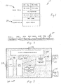
Figure 3 is a block diagram of a single-chip
SONET physical layer device 30 which is capable of
transmitting ATM cells and PPP frames in SONET SPEs in
a variety of transmission modes according to the present
invention. SONET device 30 includes control port 32,
UTOPIA bus interface port 34, a standard bus interface
port 36, and a SONET interface port 38. SONET device 30
further includes control and management interface block
40, enhanced UTOPIA interface block 42, PPP processing
block 44, SONET framer block 46 and SONET line interface
48. Control and management interface block 40 is
coupled between control port 32 and blocks 42, 44, 46
and 48.
Control and management interface block 40
includes a plurality of status registers, programmable
control registers and related control logic for
initializing the device to operate in one of the
selected transmission modes and for otherwise
controlling and managing the various blocks within
device 30. Enhanced UTOPIA interface block 42 is
coupled between UTOPIA bus interface port 34, PPP
processing block 44 and SONET framer block 46. PPP
processing block is coupled between standard bus
interface port 36, enhanced UTOPIA interface block 42
and SONET framer block 46. SONET framer block 46 is
coupled to SONET line interface 48, which is coupled to
SONET interface port 38.
1. Transmitting ATM cells in SONET SPEs
a. Standard ATM Mode
In a standard ATM mode, ATM cells are
sequentially received from an ATM Segmentation And
Reassembly (SAR) processor or cell processor (not
shown), for example, through UTOPIA bus interface port
34. Enhanced UTOPIA interface block 42 collects the
received ATM cells in an array of storage elements, such
as a stack of FIFOs. Once collected, the ATM cells are
filtered and buffered in a known manner. The resulting
cells are then passed to SONET framer block 46. In one
embodiment, enhanced UTOPIA interface block 42 is
constructed to conform with the UTOPIA Level 2 standard
specified in ATM Forum Document af-phy-0039.00. In
another embodiment, enhanced UTOPIA interface block 42
is constructed to conform with the UTOPIA Level 1
standard. Enhanced UTOPIA interface block 42 also
includes additional processing circuitry for operating
in non-standard transmission modes, as described in
greater detail below.
SONET framer block 46 receives the ATM cells
from Enhanced UTOPIA interface block 42 and places the
cells in the SPE of a SONET frame. In one embodiment of
the present invention, SONET framer block 46 is
constructed consistent with standards CCITT (ITU) 6.708,
6.709, 6.783 and I.432. The SONET frame is then passed
to line interface 48 for transmission through SONET
interface port 38. Line interface 48 is responsible for
clock generation and recovery during transmit and
receive operations. In one embodiment, line interface
48 is constructed consistent with the following
standards, ANSI T1.E1.2/92-020R2, T1.M1.3/93-005R1 and
ATM Forum atm93-1049r1.4. In another embodiment, line
interface 48 is constructed consistent with the
"SONET/SDH Interface CMOS Core (SSI)" available from LSI
Logic Corporation.
When a SONET frame is received at SONET
interface port 38, the reverse path is followed. The
received SONET frame is passed through line interface 48
to SONET framer block 46, which extracts the ATM cells
from the SONET SPE and passes the extracted ATM cells to
Enhanced UTOPIA interface block 42. Enhanced UTOPIA
interface block 42 then transmits the ATM cells to the
ATM SAR or cell processor (not shown) through UTOPIA bus
interface port 34.
b. Transmitting PPP in ATM cells in SONET
SPEs
SONET device 30 is also capable of
transmitting PPP frames in ATM cells in SONET SPEs. A
remote ATM Adaption Layer (not shown) receives a PPP
frame, segments the PPP frame into the payload fields of
a plurality of ATM cells, and generates the cell
headers. The ATM cells are then transmitted
sequentially over a UTOPIA bus to UTOPIA bus interface
port 34. Enhanced UTOPIA interface block 42 receives
the ATM cells and passes the cells to SONET framer block
46 for placement into a SONET SPE and transmission
through SONET line interface 48 and SONET interface port
38, as described above. The reverse path is also the
same as that described above.
2. Transmitting PPP from a UTOPIA interface in
SONET SPEs
In the second transmission mode, device 30 is
configured to transmit PPP from a UTOPIA interface
within SONET SPEs. This transmission mode allows a
standard ATM host processor which has no built-in or
external PPP/HDLC capability to communicate with a SONET
physical interface over a UTOPIA interface bus, and
transmit PPP frames over the SONET communication link.
As in the more traditional transmission modes discussed
above, the ATM Adaption Layer associated with the host
processor segments a protocol data unit to be
transmitted into the ATM cell payload fields, forms the
ATM cell header fields, and passes the resulting ATM
cells to device 30 through UTOPIA bus interface port 34.
Enhanced UTOPIA interface block 42 retrieves the
protocol data unit from the ATM cell payload fields by
stripping away the ATM header fields and optionally
saving the ATM header field of one of the ATM cells.
The protocol data unit and the optional remaining header
field are then passed to PPP processing block 44. In
one embodiment, the Enhanced UTOPIA interface block 42
saves the header field of the first ATM cell of the
protocol data unit.
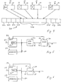
Figure 4 is a diagram illustrating the
stripping function performed by UTOPIA interface block
42. The protocol data unit is carried by a set of ATM
cells 10, which are sequentially received by block 42.
Each of the ATM cells 10 includes a cell header field 12
and a cell payload field 14. Block 42 has control
circuitry for identifying the first and last ATM cells
of the protocol data unit. Block 42 optionally stores
the header field 12 of the first ATM cell 10 and
discards the header fields 12 of all subsequent ATM
cells 10. The first header field 12 and the extracted
protocol data unit are then passed to PPP processing
block 44.
PPP processing block 44 temporarily stores the
data frame within an array of memory storage elements,
such as a FIFO, and forms a PPP frame 20 by placing the
first header field 12 and the extracted protocol data
unit in payload field 20e. PPP processing block 44 also
inserts the flag sequence in frames 20a and 20h,
calculates, checks and inserts the FCS in field 20g and
provides octet stuffing as described above. The first
header field 12 is preferably placed at the front of PPP
payload field 20e. This facilitates subsequent recovery
of the cell header fields of the remaining ATM cells.
Although PPP processing block 44 uses a fixed protocol
field 20d, the address and control fields 20b and 20c
can be negotiated away. The resulting PPP frame 20 is
then passed to SONET framer block 46 and loaded by row
into a SONET SPE, creating a large bandwidth gain.
Multiple PPP frames can be loaded into a single SONET
SPE, and a single PPP frame can be divided between two
consecutive SONET SPEs. SONET framer block 46 provides
the SONET frames to line interface block 48 for
transmission through SONET interface port 38, as
described above. In embodiments in which the receiving
circuitry does not require recovery of the ATM cells,
such as in a pure PPP application, UTOPIA interface
block 42 strips the cell header fields from all of the
ATM cells.
In the reverse direction, SONET framer block
46 receives a SONET frame from line interface block 48,
extracts the PPP frame from the SPE of the SONET frame
and passes the PPP frame to PPP processing block 44.
PPP processing block 44 extracts the ATM cell header
field from the beginning of the PPP payload field,
extracts the protocol data unit from the remainder of
the PPP payload field data and provides the ATM cell
header and the protocol data unit to enhanced UTOPIA
interface block 42. Block 42 segments the protocol data
unit into 48 octet sized pieces that fit into the ATM
cell payload fields 14. UTOPIA interface block 42 then
generates the header fields 12 for each of the ATM cells
10 based on the header field extracted from the PPP
payload field. Block 42 then transmits the ATM cells 30
through UTOPIA bus interface port 34.
With this mode of operation, the entire
protocol data unit is preferably sent in consecutive ATM
cells. Although UTOPIA interface block 42 is
constructed consistent with the UTOPIA standards listed
above, it has additional circuitry to enable the block
to detect the first ATM cell of a protocol data unit,
strip out the payload field of each ATM cell, store one
of the cell header fields, and detect the last ATM cell
of the protocol data unit in order to inform PPP
processing block 44 to end the PPP frame. In one
embodiment, PPP processing block 4 is constructed
consistent with IETF RFC 1548, RFC 1549 and ISO 3309.
Increased performance is possible by enhancing
framer block 46 to be able to strip out padding, length
and CRC bytes from the ATM AAL5 PDU trailer, prior to
PPP processing. By stripping out these bytes, less
"overhead" bytes need to be transmitted, thus improving
bandwidth efficiency. This effective gain would be a
programmable mode specific to AAL5 traffic. This
also requires that the receiving end be able to recreate
these components. Although this transmission mode is
not standard, it inter-operates easily with existing
host devices, and provides dramatic improvement in
bandwidth utilization.
3. Transmitting PPP frames directly in SONET SPEs
The third transmission mode allows a host
processor without PPP/HDLC capability to transmit and
receive protocol data units in PPP frames within SONET
SPEs through device 30. The host processor transmits
the address, control and payload fields, including the
start and end of frame indications, for a PPP frame over
a standard bus to standard bus interface port 36. The
host processor receives the same fields in return when
receiving a protocol data unit from device 30. In one
embodiment, the address and control fields for the PPP
frame are negotiated away. PPP processing block 44 of
device 30 receives the protocol data unit and the
associated fields from standard bus interface port 36,
forms a PPP frame as discussed above, and passes the PPP
frame to SONET framer block 46. SONET framer block 46
loads the PPP frame into a SONET SPE and passes the
SONET frame to line interface block 48 for transmission
through SONET interface port 38. SONET framer block 46
is of a type capable of handling streams of data such
that a PPP payload can be loaded by row into the SONET
SPE.
Figures 5 and 6 are diagrams illustrating the
SONET physical layer device of the present invention
coupled to a host processor for implementing the
transmission modes discussed above. In Figure 5, host
processor 50 is coupled to UTOPIA interface port 34
through an ATM SAR device 52. Host processor 50 has a
port 54 for transmitting and receiving data units
according to a selected protocol. For example, port 54
may be coupled to an Ethernet communications link. Host
processor 50 has a DMA controller 56 which stores the
protocol data units in memory 58, over bus 60. Host
processor 50 also has a control output which is coupled
to control port 32 of device 30. Host processor 50 uses
the control output for configuring device 30 to operate
in one of the selectable transmission modes. For
example, with the circuit shown in Figure 5, device 30
can be programmed to operate in one of the first two
transmission modes discussed above, including
transmitting ATM cells in SONET SPEs or PPP frames in
ATM cells in SONET SPEs, and transmitting PPP frames
from a UTOPIA interface in SONET SPEs. With each of
these transmission modes, DMA controller 56 retrieves
protocol data unit to be transmitted from memory 58 and
provides data unit to ATM SAR circuit 52. ATM SAR
circuit 52 segments the data unit into 48 octet-sized
pieces that fit into the ATM cell payload fields and
generates a header field for each ATM cell. ATM SAR
circuit 60 then transmits the ATM cells to UTOPIA bus
interface port 34 over UTOPIA bus 62.
In Figure 6, bus 60 is coupled directly to
standard bus interface port 36 of device 30. The same
reference numerals are used in Figure 6 as were used in
Figure 5 for the same or similar elements. The control
output of host processor 50 is coupled to control port
32 of device 30, and host processor 50 configures device
30 to transmit PPP frames directly in SONET SPEs. Host
processor 50 transmits the address, control and payload
fields for a PPP frame over bus 60 through DMA
controller 56 and memory 58. Host processor 50 receives
the same fields in return when receiving a data unit
from device 30. PPP processing block 44 in device 30
receives the data unit and its associated fields through
standard bus interface port 36, forms a PPP frame and
passes the PPP frame to SONET framer block 46 for
transmission in a SONET SPE as discussed above.
5. Conclusion
The SONET physical device of the present
invention is constructed on a single integrated circuit,
which reduces the board space required to implement the
circuit and the resulting cost of its manufacture. The
device inter-operates with multiple standard and non-standard
data encapsulation mechanisms, and allows
packet transmission using the PPP protocol over a SONET
communication link for maximum bandwidth utilization.
SONET communication links are expensive and
crowded with data traffic. The SONET physical layer
device of the present invention allows data traffic to
be transported readily in local or campus networks
according to RFC 1619 with a large performance gain for
little or no increased cost. Independent studies have
shown that the protocol data units (PDUs) presented to
Frame Relay networks as well as ATM AAL5 layers for
transport across ATM networks are almost always one of
three sizes, 64 octets, 1500 octets and 384 octets. 64
octets is the size of acknowledgement packets used in
Ethernet and other protocols. 1500 octets is the
maximum size protocol data unit for non-enhanced
Ethernet. 384 octets is the size theorized to be a
result of legacy data traffic from protocols with a
maximum 384 octet data bit size. This size information
was used to calculate efficiency of data transport with
the various transmission modes of the present invention.
In the "standard" ATM mode, ATM cells are
loaded into a SONET (STS-1) SPE more or less directly.
Efficiency of transport of the common data unit sizes in
the ATM mode are shown in Table 1:
| Size of PDU | # of ATM Cells required for Transport | Total Octets in ATM Cells | Octet Efficiency of Cells (Oe) | SONET Efficiency (783 Oe)/810 |
| 64 | 2 | 106 | 60.37% | 58.36% |
| 384 | 9 | 477 | 64.81% | 62.65% |
| 1500 | 32 | 1696 | 88.44% | 85.49% |
The transport efficiency of a 48-octet payload
in a 53-octet ATM cell is 90.57%. This is the number
typically quoted for ATM transport systems. However,
the decrease in efficiency shown in Table 1 comes from
the necessity of adding more protocol layers (the AAL5
layer) to support the various size PDUs and to provide
error checking across the PDU. Additional overhead is
incurred from mapping the ATM cells into the SONET
frame.
Transporting PPP frames in ATM cells over
SONET consists of adding the PPP flag sequences, control
fields, etc., to the PDU as well as performing byte
stuffing. The PPP processed PDU is then segmented into
standard ATM cells for transport. For the purposes of
the following efficiency calculations, it was assumed
that the control overhead could be negotiated down to 7
octets, and that byte stuffing would only be required
for 2 octet values uniformly across the PDU (or one out
of 128 octets would require stuffing). Table 2 shows
the transport efficiency for this mode of operation. In
this mode of operation, a layer of PPP processing has
been added but there has been no gain in transport
efficiency.
| Size of PDU | Size of PPP Processed PDU | # of ATM cells Required for Transport | Total Octets in ATM cells | Octet Efficiency of cells (Oe) | SONET Efficiency (783*Oe)/810 |
| 64 | 72 | 2 | 106 | 60.37% | 58.36% |
| 384 | 394 | 9 | 477 | 64.81% | 62.65% |
| 1500 | 1519 | 32 | 1696 | 88.44% | 85.49% |
Transporting PPP frames from a UTOPIA
interface over SONET results in a significant increase
in efficiency, as shown in Table 3. The increase in
efficiency is gained by stripping the ATM cell headers
from the PDU.
| Size of PDU | Size of PPP Processed PDU (4 bytes added for first ATM cell header) | Octet Efficiency of cells (Oe) | SONET Efficiency (783*Oe)/810) |
| 64 | 76 | 84.21% | 81.40% |
| 384 | 398 | 96.48% | 93.26% |
| 1500 | 1523 | 98.49% | 95.21% |
Transporting PPP direct over SONET results in
essentially the same transport efficiencies as those
shown in Table 3. The 4 bytes added to recover the ATM
cell header in the previous mode of operation would be
replaced by another addressing mechanism, but the
efficiencies would remain substantially the same. The
primary distinction between these two modes of operation
is that the ATM segmentation and reassembly function is
totally removed, and the data no longer has to pass
through the UTOPIA bus interface.
The SONET physical layer device of the present
invention can be constructed to operate at different
transmission rates, such as STS-1, STS-3C and STS-12,
using the same principals. The device can be configured
with its surrounding components to operate in one of the
selectable transmission modes during board level design
or can be programmed during operation. The device can
be constructed as a core or a macro within a larger
integrated circuit design specification. Also, the
device can be constructed with multiplexed bus lines in
order to achieve a smaller number of pins on the
integrated circuit package. In one embodiment, the
device is constructed without a line interface block.
In this embodiment, an external line driver is used,
which allows the use of varying types of line drivers.
In addition, multiple instances, such as four or eight,
of the device can be placed on a single integrated
circuit to provide multiple transmission channels for a
line card router, for example.
Although the present invention has been
described with reference to preferred embodiments,
workers skilled in the art will recognize that changes
may be made in form and detail without departing from
the spirit and scope of the invention.