EP0880130A2 - Optical disk having increased erasure efficiency - Google Patents
Optical disk having increased erasure efficiency Download PDFInfo
- Publication number
- EP0880130A2 EP0880130A2 EP98303960A EP98303960A EP0880130A2 EP 0880130 A2 EP0880130 A2 EP 0880130A2 EP 98303960 A EP98303960 A EP 98303960A EP 98303960 A EP98303960 A EP 98303960A EP 0880130 A2 EP0880130 A2 EP 0880130A2
- Authority
- EP
- European Patent Office
- Prior art keywords
- optical disk
- groove
- recording
- recited
- groove depth
- Prior art date
- Legal status (The legal status is an assumption and is not a legal conclusion. Google has not performed a legal analysis and makes no representation as to the accuracy of the status listed.)
- Withdrawn
Links
- 230000003287 optical effect Effects 0.000 title claims abstract description 135
- 230000008859 change Effects 0.000 claims abstract description 38
- 239000000758 substrate Substances 0.000 claims abstract description 38
- 239000010410 layer Substances 0.000 claims description 78
- VYPSYNLAJGMNEJ-UHFFFAOYSA-N silicon dioxide Inorganic materials O=[Si]=O VYPSYNLAJGMNEJ-UHFFFAOYSA-N 0.000 claims description 36
- 229910052681 coesite Inorganic materials 0.000 claims description 31
- 229910052906 cristobalite Inorganic materials 0.000 claims description 31
- 239000000377 silicon dioxide Substances 0.000 claims description 31
- 229910052682 stishovite Inorganic materials 0.000 claims description 31
- 229910052905 tridymite Inorganic materials 0.000 claims description 31
- 150000004767 nitrides Chemical class 0.000 claims description 10
- 239000004033 plastic Substances 0.000 claims description 7
- 229920003023 plastic Polymers 0.000 claims description 7
- 239000002344 surface layer Substances 0.000 claims description 4
- 230000003746 surface roughness Effects 0.000 claims description 3
- 230000001627 detrimental effect Effects 0.000 abstract description 9
- 235000019592 roughness Nutrition 0.000 description 24
- IJGRMHOSHXDMSA-UHFFFAOYSA-N Atomic nitrogen Chemical compound N#N IJGRMHOSHXDMSA-UHFFFAOYSA-N 0.000 description 20
- 230000005540 biological transmission Effects 0.000 description 15
- 238000005259 measurement Methods 0.000 description 15
- 239000011241 protective layer Substances 0.000 description 12
- 229910052757 nitrogen Inorganic materials 0.000 description 10
- 238000002425 crystallisation Methods 0.000 description 8
- 230000008025 crystallization Effects 0.000 description 8
- 238000011156 evaluation Methods 0.000 description 8
- 229910000618 GeSbTe Inorganic materials 0.000 description 7
- 238000010586 diagram Methods 0.000 description 7
- 230000000694 effects Effects 0.000 description 6
- 238000000034 method Methods 0.000 description 6
- 238000001020 plasma etching Methods 0.000 description 6
- 238000010791 quenching Methods 0.000 description 5
- 230000000171 quenching effect Effects 0.000 description 5
- 238000010583 slow cooling Methods 0.000 description 5
- 230000007423 decrease Effects 0.000 description 4
- 239000011521 glass Substances 0.000 description 4
- 239000000463 material Substances 0.000 description 4
- 239000011347 resin Substances 0.000 description 4
- 229920005989 resin Polymers 0.000 description 4
- 239000004065 semiconductor Substances 0.000 description 4
- 229910045601 alloy Inorganic materials 0.000 description 3
- 239000000956 alloy Substances 0.000 description 3
- 238000005520 cutting process Methods 0.000 description 3
- 238000005530 etching Methods 0.000 description 3
- 229910052751 metal Inorganic materials 0.000 description 3
- 239000002184 metal Substances 0.000 description 3
- 229920003229 poly(methyl methacrylate) Polymers 0.000 description 3
- 239000004926 polymethyl methacrylate Substances 0.000 description 3
- 230000009467 reduction Effects 0.000 description 3
- 238000004833 X-ray photoelectron spectroscopy Methods 0.000 description 2
- 230000015572 biosynthetic process Effects 0.000 description 2
- 230000000052 comparative effect Effects 0.000 description 2
- 238000005286 illumination Methods 0.000 description 2
- 230000006872 improvement Effects 0.000 description 2
- 238000001746 injection moulding Methods 0.000 description 2
- 230000001678 irradiating effect Effects 0.000 description 2
- 230000005415 magnetization Effects 0.000 description 2
- 238000004519 manufacturing process Methods 0.000 description 2
- 239000002991 molded plastic Substances 0.000 description 2
- 238000000465 moulding Methods 0.000 description 2
- 229920002120 photoresistant polymer Polymers 0.000 description 2
- 239000004417 polycarbonate Substances 0.000 description 2
- 229920000515 polycarbonate Polymers 0.000 description 2
- 229920005668 polycarbonate resin Polymers 0.000 description 2
- 239000004431 polycarbonate resin Substances 0.000 description 2
- 230000008569 process Effects 0.000 description 2
- 239000010453 quartz Substances 0.000 description 2
- 230000003252 repetitive effect Effects 0.000 description 2
- 238000000682 scanning probe acoustic microscopy Methods 0.000 description 2
- 238000004544 sputter deposition Methods 0.000 description 2
- 229910017150 AlTi Inorganic materials 0.000 description 1
- 229910005542 GaSb Inorganic materials 0.000 description 1
- 230000005374 Kerr effect Effects 0.000 description 1
- 239000004793 Polystyrene Substances 0.000 description 1
- 238000010521 absorption reaction Methods 0.000 description 1
- 238000009825 accumulation Methods 0.000 description 1
- 230000001154 acute effect Effects 0.000 description 1
- 150000004770 chalcogenides Chemical class 0.000 description 1
- 229910052804 chromium Inorganic materials 0.000 description 1
- 238000007796 conventional method Methods 0.000 description 1
- 238000001816 cooling Methods 0.000 description 1
- 229910052802 copper Inorganic materials 0.000 description 1
- 230000001186 cumulative effect Effects 0.000 description 1
- 238000013461 design Methods 0.000 description 1
- 150000002222 fluorine compounds Chemical class 0.000 description 1
- 239000007789 gas Substances 0.000 description 1
- 229910052737 gold Inorganic materials 0.000 description 1
- 238000002347 injection Methods 0.000 description 1
- 239000007924 injection Substances 0.000 description 1
- 238000002844 melting Methods 0.000 description 1
- 230000008018 melting Effects 0.000 description 1
- 150000001247 metal acetylides Chemical class 0.000 description 1
- 150000002739 metals Chemical class 0.000 description 1
- 239000000203 mixture Substances 0.000 description 1
- 229910052759 nickel Inorganic materials 0.000 description 1
- 239000000049 pigment Substances 0.000 description 1
- 230000010287 polarization Effects 0.000 description 1
- 229920005672 polyolefin resin Polymers 0.000 description 1
- 229920002223 polystyrene Polymers 0.000 description 1
- 238000001552 radio frequency sputter deposition Methods 0.000 description 1
- 229910052761 rare earth metal Inorganic materials 0.000 description 1
- 150000002910 rare earth metals Chemical class 0.000 description 1
- 238000012827 research and development Methods 0.000 description 1
- 229910052710 silicon Inorganic materials 0.000 description 1
- 239000002356 single layer Substances 0.000 description 1
- 229910052719 titanium Inorganic materials 0.000 description 1
- 238000013518 transcription Methods 0.000 description 1
- 230000035897 transcription Effects 0.000 description 1
- 229910052723 transition metal Inorganic materials 0.000 description 1
- 239000012780 transparent material Substances 0.000 description 1
Images


Classifications
-
- G—PHYSICS
- G11—INFORMATION STORAGE
- G11B—INFORMATION STORAGE BASED ON RELATIVE MOVEMENT BETWEEN RECORD CARRIER AND TRANSDUCER
- G11B7/00—Recording or reproducing by optical means, e.g. recording using a thermal beam of optical radiation by modifying optical properties or the physical structure, reproducing using an optical beam at lower power by sensing optical properties; Record carriers therefor
- G11B7/24—Record carriers characterised by shape, structure or physical properties, or by the selection of the material
- G11B7/2407—Tracks or pits; Shape, structure or physical properties thereof
- G11B7/24073—Tracks
- G11B7/24076—Cross sectional shape in the radial direction of a disc, e.g. asymmetrical cross sectional shape
-
- G—PHYSICS
- G11—INFORMATION STORAGE
- G11B—INFORMATION STORAGE BASED ON RELATIVE MOVEMENT BETWEEN RECORD CARRIER AND TRANSDUCER
- G11B7/00—Recording or reproducing by optical means, e.g. recording using a thermal beam of optical radiation by modifying optical properties or the physical structure, reproducing using an optical beam at lower power by sensing optical properties; Record carriers therefor
- G11B7/007—Arrangement of the information on the record carrier, e.g. form of tracks, actual track shape, e.g. wobbled, or cross-section, e.g. v-shaped; Sequential information structures, e.g. sectoring or header formats within a track
- G11B7/00718—Groove and land recording, i.e. user data recorded both in the grooves and on the lands
-
- G—PHYSICS
- G11—INFORMATION STORAGE
- G11B—INFORMATION STORAGE BASED ON RELATIVE MOVEMENT BETWEEN RECORD CARRIER AND TRANSDUCER
- G11B7/00—Recording or reproducing by optical means, e.g. recording using a thermal beam of optical radiation by modifying optical properties or the physical structure, reproducing using an optical beam at lower power by sensing optical properties; Record carriers therefor
- G11B7/24—Record carriers characterised by shape, structure or physical properties, or by the selection of the material
- G11B7/2407—Tracks or pits; Shape, structure or physical properties thereof
- G11B7/24073—Tracks
- G11B7/24079—Width or depth
-
- G—PHYSICS
- G11—INFORMATION STORAGE
- G11B—INFORMATION STORAGE BASED ON RELATIVE MOVEMENT BETWEEN RECORD CARRIER AND TRANSDUCER
- G11B7/00—Recording or reproducing by optical means, e.g. recording using a thermal beam of optical radiation by modifying optical properties or the physical structure, reproducing using an optical beam at lower power by sensing optical properties; Record carriers therefor
- G11B7/004—Recording, reproducing or erasing methods; Read, write or erase circuits therefor
- G11B7/0055—Erasing
- G11B7/00557—Erasing involving phase-change media
-
- G—PHYSICS
- G11—INFORMATION STORAGE
- G11B—INFORMATION STORAGE BASED ON RELATIVE MOVEMENT BETWEEN RECORD CARRIER AND TRANSDUCER
- G11B7/00—Recording or reproducing by optical means, e.g. recording using a thermal beam of optical radiation by modifying optical properties or the physical structure, reproducing using an optical beam at lower power by sensing optical properties; Record carriers therefor
- G11B7/004—Recording, reproducing or erasing methods; Read, write or erase circuits therefor
- G11B7/006—Overwriting
Definitions
- the present invention relates to an optical disk, and, more particularly, the present invention relates to an optical disk having improved erasure efficiency.
- Optical disks have recently come into general use as high capacity memory in consumer electronics, calculators, and the like. Furthermore, the next generation of optical disks requires additional increased capacity, higher rotational speed, overwriting, and the like to accommodate the requirements of the multimedia age, and the greater amount and diversity of information associated therewith.
- the signals of the adjacent track tend to be erased by cross-erasure, or the signals projecting into the adjacent track tend to become recorded, and cross-writing and the like tend to occur.
- the effects of cross-erasure and cross-writing are cumulative, the influence of the detrimental effects described above is very evident in an optical disk which repeats recording and playback.
- a low CNR carrier/noise ratio
- the erasure characteristics also decrease accompanying a narrowing of the track pitch. More particularly, if recording marks are written to the full width of the narrow track so that they project a little, then at the time of overwriting erasure remnants occur causing the decrease in erasure characteristics.
- the conventional optical disk which performs land/groove recording is limited to a track pitch of about 0.8-0.7 ⁇ m, and it is considered difficult to further narrow the track pitch. Further, the reduction of cross-writing, cross-erasure and noise are important problems which are not limited to optical disks having land portions and groove portions.
- optical recording and playback systems having high density, high capacity, high access speed, high recording and playback speeds, and the like characteristics, have recently been put to practical use. Increasing amounts of research and development time is being devoted to improve these optical recording and playback systems.
- the optical information recording media used for the conventional optical recording and playback systems are in the form of disks, and are broadly classified into a read-only type for only playback dedicated use and a recordable type.
- the read-only type of optical recording medium has projections or hollows, referred to as pits, formed in a recording layer, and information is represented according to the presence or absence of the pits, or information is represented according to the length of the pits.
- the recordable type of optical recording medium includes a type which can record one time only (referred to as write-once or DRAW), and a type which can repeat recording and erasure a number of times.
- the former type of optical recording medium includes a recording layer consisting of Te, Te-C, Te-Se-Pb, resins which include pigments, and the like, in which holes (pits) open when illuminated with a laser beam. Information is represented by the presence or absence of the pit or by the length of the pit.
- the latter type of optical recording medium in practical use includes a phase change type (crystalline-amorphous) and a magneto-optical type.
- the phase change type has a crystalline phase recording layer consisting of TeO 2 -Te-Ge, GeSbTe, or InSe.
- a crystalline phase recording layer consisting of TeO 2 -Te-Ge, GeSbTe, or InSe.
- the crystalline phase is heated to the melting point or above, and by rapid cooling forms marks in the amorphous state. Information is represented by the presence or the absence of these marks or by the length of the marks.
- a laser beam for use in erasure heats the marks, which are in an amorphous state, to the crystallization temperature or above, and brings about crystallization (erasure) by slow cooling. Recording of information is performed by illuminating the optical recording medium with a recording laser beam immediately after the erasure laser beam. Thus, recording and erasure are repeated.
- the magneto-optical type of optical recording medium includes a recording layer consisting of a magnetic thin layer which can be perpendicularly magnetized. Initialization is performed to make the direction of magnetization uniformly upward or downward. Then, upon illuminating the magneto-optical recording medium with a laser beam and simultaneously applying a recording magnetic field, a mark is formed in which the direction of magnetization is reversed. Information is represented by the presence or absence of these marks or by their length. When the marks are illuminated with linearly polarized light (weak laser beam), the plane of polarization of the reflected light or the transmitted light is rotated ⁇ k . This is termed the Kerr effect or the Faraday effect.
- the portions of "ground" outside the marks rotates by - ⁇ k . Consequently, by passing the reflected light or transmitted light through a polarizing element (detector), the marks can be interpreted as a change in the amount of light. The change in the amount of light can be converted to a change in the intensity of an electrical signal by a photoelectric converter.
- magneto-optical recording layers include rare earth - transition metal alloys, for example, TbFe, GdFe, GdCo, DyFe, GdTbFe, GdFeCo and the like single layer films, or GdFe/TbFe, GdFeCo/TeFeCo and the like 2-layer films.
- rare earth - transition metal alloys for example, TbFe, GdFe, GdCo, DyFe, GdTbFe, GdFeCo and the like single layer films, or GdFe/TbFe, GdFeCo/TeFeCo and the like 2-layer films.
- an optical disk on which data is recorded in respective land portions and groove portions using a phase change between amorphous and crystalline including a disk substrate having a refractive index of n, wherein ⁇ is the wavelength of an illuminating light, such as a laser light source, a groove depth, which is a difference in level between the land portions and the groove portions, is equal to or greater than ⁇ /(3.78n) and a groove sidewall has a roughness width of 50 nm or less.
- the heat transmission distance between the land portions and the groove portions is made long. Because the heat transmission distance between the land portions and the groove portions is lengthened, heat caused by the illumination of the illuminating light is poorly transmitted to the adjacent tracks, and cross-erasure, cross-writing and similar detrimental effects due to heat transmission are reduced.
- the land portions and groove portions both tend to accumulate heat. Therefore, while erasing a record mark, an amorphous mark in the vicinity of the crystallization temperature accumulates heat for a long time. As a result of the accumulation of heat, the crystallization efficiency of the amorphous mark increases, and the erasure efficiency increases.
- the value of the cross-writing resistance Pw/Pp (described hereinbelow) is maintained by setting the groove depth equal to or greater than ⁇ /(3.78n) when the track pitch is about 0.6 ⁇ m.
- the CNR value of 45 dB is a value which satisfies the standard CNR value of 45 dB set by ISO standards, and the like.
- the optical disk includes a groove sidewall with a roughness width of 20 nm or less.
- a roughness width of 20 nm or less.
- the optical disk has a track pitch that is narrower than 1.18 ⁇ .
- the optical disk has a groove depth in the range of ⁇ /(3.78n) to ⁇ /(1.13n).
- the optical disk has groove depth of ⁇ /(3n).
- the optical disk has a groove depth of ⁇ /(3n) + ⁇ /(2n) ⁇ .
- the optical disk has a groove depth of ⁇ /(6n) + ⁇ /(2n) ⁇ .
- the cross-talk from adjacent tracks can be made a minimum.
- the optical disk includes a groove sidewall having a taper angle of 60 degrees or more.
- the groove sidewall is formed with a taper angle. Because of the taper angle, the width of the groove seen from the optical pickup enlarges as the groove depth deepens. At this time, because signals from the tracks of both sides are recorded projecting into the groove sidewalls, cross-writing resistance is worsened to the extent of cross-writing to the groove sidewalls.
- the optical disk includes a groove sidewall having a taper angle of 80 degrees or more.
- the optical disk includes a groove sidewall having a taper angle of 84 degrees or more.
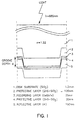
- FIG. 1 is a cross-sectional diagram of a basic structure (quenching structure) of a phase change type of optical disk in accordance with embodiments of the invention.
- FIG. 2 is a graph showing the values of erasure efficiency in the case of various settings of erasure power in accordance with embodiments of the invention.
- FIG. 3 is a graph showing a relationship between the cross-writing resistance Pw/Pp and groove depth in accordance with embodiments of the invention.
- FIG. 4 is a graph showing a relationship between the cross-writing resistance Pw/Pp and the track pitch in accordance with embodiments of the invention.
- FIG. 5 is a graph showing a relationship between groove depth and crosstalk in accordance with embodiments of the invention.
- FIG. 6 is a graph showing a relationship between crosstalk and various values of recording power in accordance with embodiments of the invention.
- FIGS. 7A and 7B are electron microscope photographs of a stamper surface in accordance with embodiments of the invention.
- FIG. 8 is a diagram showing an improvement effect by reducing the roughness of the groove sidewalls in accordance with embodiments of the invention.
- FIG. 9 is a diagram illustrating a taper angle of the groove sidewalls in accordance with embodiments of the invention.
- FIG. 10 is a graph showing a relationship between the cross-writing resistance Pw/Pp and various values of the taper angle in accordance with embodiments of the invention.
- FIG. 11 is a cross sectional diagram showing the basic structure (quenching structure) of a phase change type of optical disk in accordance with embodiments of the invention.
- FIG. 12 is a graph showing a relationship between signal level and pit depth in accordance with embodiments of the present invention.
- FIG. 1 is a cross-sectional diagram (quenching structure) of a phase change type of optical disk in accordance with embodiments of the present invention.
- a groove is formed in spiral form in the surface of the disk substrate 1, creating land portions and groove portions.
- a groove depth d is set to a value of 120 nm or more, deeper than the prior art groove depth of 40-85 nm.
- the optical disk includes a first protective layer 2, a recording layer 3, a second protective layer 4, and a reflective layer 5 formed in succession on the surface of the disk substrate 1.
- the first protective layer 2 is preferably a 135 nanometer (nm) thick layer formed of ZnS-SiO 2 .
- the recording layer 3 is preferably a 25 nm thick layer formed of a GeSbTe alloy.
- the second protective layer 4 is preferably a 20 nm thick layer formed of ZnS-SiO 2 .
- the reflective layer 5 is preferably a 150 nm thick layer formed of Al.
- An optical pickup (not shown in the drawing) used for evaluation measurement of the optical disk has a laser light wavelength of 685 nm, and an aperture number (NA) of the objective lens 0.6.
- the erasure efficiency of the optical disk was measured when performing overwriting.
- the erasure efficiency characteristics of the optical disk when overwriting was performed will now be described below in accordance with the results of the measurement.
- erasure efficiency was measured according to the following operations:
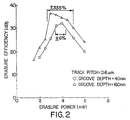
- FIG. 2 is a graph illustrating a comparative example of the values of erasure efficiency in the case of various settings of the erasure power.
- the triangles shown in FIG. 2 indicate the erasure efficiency in an optical disk having a groove depth of 160 nm in accordance with the present preferred embodiment of the invention.
- the erasure efficiency of the optical disk in accordance with the present preferred embodiment of the invention is increased by 3-10 dB overall in comparison with the prior art optical disk.
- the erasure efficiency at the time of overwriting is increased resulting in the following advantages.
- the thermal transmission path between land portions and groove portions becomes long.
- the transmission of irradiation heat to adjacent tracks becomes poor, and heat tends to collect in the tracks. Therefore, the spread of heat when recording and when erasing is limited to about the same range, and erasure remnants of the mark periphery are less likely to occur.
- the heat transmission path between the land portions and the groove portions is made long, heat becomes likely to collect on a track. Because of the heat collecting on a track, when erasing a recording mark the amorphous portions remain in the vicinity of the crystallization temperature for a long time. As a result, the crystallization efficiency of an amorphous portion is increased, and the erasure efficiency increases. In the above-described manner, the erasure efficiency is improved by making the groove depth deep, and a narrower track pitch can be designed resulting in increased transmission rates.
- the cross-writing resistance of the optical disk was measured. A description of the results of the measurement of the cross-writing resistance will now be provided below.
- Cross-writing resistance is measured according to the following operations. Firstly, the whole optical disk is made a crystalline structure (erasure state). For one (1) track on the optical disk, single frequency recording pits having a length of 0.4 ⁇ m are recorded at linear speed of 5 m/sec. The value of the recording power is determined at this time such that the CNR and the erasure efficiency become optimum. The optimum recording power is Pp.
- single frequency recording pits having a length of about 0.43 ⁇ m are recorded for the adjacent groove portions on both sides, respectively, one-hundred (100) times.
- CNR measurement is performed.
- the value of the recording power Pw at which the CNR begins to fall 0.5 dB is determined.
- the ratio of the recording power to the optimum recording power Pw/Pp is calculated and is taken to be the cross-writing resistance.
- the cross-writing resistance is one (1) or less
- the CNR has fallen by 0.5 dB or more. Because of the drop in CNR, when the cross-writing resistance Pw/Pp is one (1) or less, it is about not suitable for practical use.
- the cross-writing resistance Pw/Pp is one (1) or more
- the drop of the CNR in the adjacent tracks can be kept to 0.5 dB or less.
- the region in which the cross-writing resistance Pw/Pp is one (1) or more is the region in which practical use is possible.
- the cross-writing resistance Pw/Pp is preferably 1.1 or more.
- FIG. 3 is a graph illustrating respective measurement results of the cross-writing resistance Pw/Pp for optical disks with the track pitch and the groove depth variously set.
- the cross-writing resistance Pw/Pp increases as the groove depth becomes deeper.
- a value for the cross-writing resistance Pw/Pp of one (1) or more can be maintained.
- a track pitch of 0.6 ⁇ m or less can be realized, exceeding the prior art track pitch limit of 0.7 ⁇ m.
- the critical condition of a groove depth of 120 nm is found by optically converting ⁇ /(3.78n), wherein the wavelength of the laser light is ⁇ , and the refractive index of the disk substrate is n.
- FIG. 4 is a graph illustrating the relationship between the cross-writing resistance Pw/Pp and the track pitch in accordance with embodiments of the present invention.
- FIG. 5 is a graph illustrating a relationship between groove depth and crosstalk in accordance with embodiments of the present invention. As shown in FIG. 5, the measurement values are indicated by black circles and the solid line indicates calculated values.
- FIG. 6 is a graph illustrating a relationship between crosstalk and recording power in accordance with the present invention. As shown in FIG. 6, the circles represent measurement data when the groove depth is set to ⁇ /(6n), as in the prior art. The triangles in FIG. 6 represent measurement data when the groove depth is set to ⁇ /(3n).
- the crosstalk when the groove depth is ⁇ /(3n), even when the recording power changes greatly, the crosstalk only changes slightly. More particularly, the crosstalk only changes slightly because the deep groove depth causes the projection of the recording mark width to be limited by the groove sidewalls.
- the change in crosstalk during normal conditions is nominal, and, even during unfavorable conditions, such as large changes of the recording power of the optical pickup unit, the crosstalk can be strongly suppressed.
- FIG. 7A is a photograph of groove walls having a roughness width of about 150 nm.
- the roughness width of the groove sidewalls is defined as follows.
- the groove sidewalls include minute plural irregularities (roughnesses).
- the roughness width of the groove sidewalls refers to the dimension (i.e., height, depth or width) of a convex or concave portion of the irregularity. Accordingly, a roughness width of 50 nm or less means that the height, depth or width of a convex portion or a concave portion is 50 nm or less. Roughness can be observed using a high-resolution scanning electron microscope (HR-SEM), STM, AFM or the like.
- HR-SEM high-resolution scanning electron microscope
- FIG. 7B is a photograph of groove walls having a roughness width of 20 nm or less. Furthermore, a stamper of FIG. 7B was prepared by normalizing each factor for the well known mastering process.
- FIG. 8 is a diagram showing the improvement effect achieved by reducing the roughness width of the groove sidewalls in accordance with the present invention.
- a roughness width of the groove sidewalls is 150 nm or more, and at the noise level of playback noise (-60 dBm)
- the CNR is 42 dB.
- the noise level of playback noise is improved as far as (-63 dBm)
- the CNR is improved to 45 dB.
- the roughness width of the groove sidewalls is 20 nm or less, the noise level of playback noise is improved to (-66 dBm), and the CNR is improved to 48 dB.
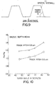
- FIG. 9 is a diagram defining the taper angle of the groove sidewalls in accordance with embodiments of the present invention. As shown in FIG. 9, the acute angle ⁇ between the surface of the groove sidewall and the substrate surface of the disk is defined as the taper angle ⁇ .
- FIG. 10 is a graph illustrating the cross-writing resistance Pw/Pp with respect to the taper angle ⁇ when the taper angle ⁇ is variously set in accordance with embodiments of the present invention. Furthermore, the groove depth of the optical disk used for the measurements shown in FIG. 10 is 180 nm.
- the cross-writing resistance increases as the taper angle becomes steeper (closer to 90°).
- the cross-writing resistance increases as the taper angle is made steep because the width of the groove seen from the optical pickup becomes narrow, and the crosswriting portion with respect to the groove sidewall decreases. More specifically, when the taper angle is set to 60° or more, even at a track pitch of 0.5 ⁇ m, the cross-writing resistance can be maintained at a value of one (1) or more, at which practical use is possible.
- the taper angle is set to 80° or more, even at a track pitch of 0.5 ⁇ m, the cross-writing resistance can be maintained at a value of 1.1 or more, at which practical use is possible.
- the taper angle is set to 84° or more, the width of the groove sidewalls seen from the track pitch can be neglected, and the cross-writing resistance increases sharply.
- the optical disk is a phase change type of optical disk including a recording layer 3 which is preferably GeSbTe, and having ZnS-SiO 2 layers including nitrides formed in the layers above and below the recording layer 3.
- a recording layer 3 which is preferably GeSbTe
- ZnS-SiO 2 layers including nitrides formed in the layers above and below the recording layer 3.
- the ZnS-SiO 2 layers of the phase change optical disk are formed by RF sputtering.
- the gas pressure at the time of sputtering is controlled to about 0.1 mTorr - 10 mTorr.
- the nitride is added to the ZnS-SiO 2 layer by the introduction of Ar and N 2 during the formation of the ZnS-SiO 2 layer.
- Sputtering is performed at a quantity of N 2 of 0.1 ⁇ Torr or more. Further, the molar ratio of the ZnS and SiO 2 in the formed ZnS-SiO 2 layer is 8:2.
- Disk A a disk having nitride added to the ZnS-SiO 2 layer in the layers above and below the recording layer in accordance with the present preferred embodiment of the invention
- Disk B a conventional disk recording medium manufactured by a conventional method
- the wavelength ( ⁇ ) of a semiconductor of the optical pickup used in the evaluation of the disks is 685 nm, and a condensing lens is used having a numerical aperture (NA) 0.6.
- erasure efficiency is measured according to the following operations. Firstly, (1) a 3T mark is recorded, (2) the 3T mark is read, and (3) an 8T mark is overwritten. The above operations (1)-(3) are then repeated one-hundred (100) times. After repeating the above operations (1)-(3), a 3T mark is recorded. A comparison of the 8T signal and the 3T signal is then made, and the erasure efficiency is respectively determined.
- Disk A and Disk B are compared, it is determined that the erasure efficiency of Disk A increased by 3 dB or more. Furthermore, when the groove depth is about 160 nm, it is determined that there is a further increase of erasure efficiency in Disk A.
- the optical disk (Disk A) having layers with nitride added to the ZnS-SiO 2 in the layers above and below the recording layer 3 showed no change in jitter, even when recording is repeated 170,000 times and more. Further, when the track pitch is 0.6 ⁇ m, it was determined that the overwrite cycle characteristics of Disk A increased in comparison with Disk B.
- the nitrogen concentration in the film i.e., the layers above and below the recording layer
- AES auger electron spectroscopy
- XPS x-ray photoelectron spectroscopy
- the average nitrogen concentration in the film is preferably about 0.01 - 40 atom%.
- providing the average nitrogen concentration in the ZnS-SiO 2 layer at the interface of the recording layer produced much better repetitive recording characteristics than nitrogen in the interior of the ZnS-SiO 2 layer.
- providing the average nitrogen concentration in the ZnS-SiO 2 layer within 10 nm from the interface of the recording layer produced much better recording characteristics than nitrogen in the interior of the ZnS-SiO 2 layer.
- providing the average nitrogen concentration in a portion of the ZnS-SiO 2 layer having a thickness of 1 nm from the interface of the ZnS-SiO 2 layer and the recording layer was determined to be preferable to providing two or more times the average nitrogen concentration in a portion of the ZnS-SiO 2 outside of the 1 nm thick portion.
- the film can be manufactured such that the nitrogen concentration becomes gradually smaller from the interface of the ZnS-SiO 2 layer and the recording layer.
- a plastic substrate is used as the disk substrate 1.
- the plastic substrate is generally PMMA (polymethyl methacrylate), polycarbonate, polystyrene, resins and the like transparent materials.
- the plastic substrate is preferably molded from polycarbonate resin by an injection molding method. Further, a surface layer portion of the molded substrate and an interior of the molded substrate are preferably molded such that the respective densities are different.
- a substrate having a diameter of 120 mm, and a thickness of 0.6 mm was molded for use in digital versatile disks (DVDs) and the like. Molding of the substrate is performed at an injection pressure of the resin during molding of 30t, with a metal mold at 120°C, a resin temperature of 340°C or more, and a cycle time of 12 seconds.
- the molded plastic substrate has a different density in the surface portion in comparison with an interior portion.
- the surface portion preferably has a thickness in a range of about 60-500 nm. The thickness of the surface portion can be confirmed by HR-SEM.
- Phase change disks having a structure (substrate/ZnS-SiO 2 /GeSbTe/ZnS-SiO 2 /AlTi) were prepared using the molded plastic substrate, and having a groove depth, which is the difference in level between the land portions and the groove portions, of ⁇ /(3.78n) or more. The characteristics of the phase change disks thus prepared were then evaluated.
- the wavelength ( ⁇ ) of the semiconductor of the optical pickup used in the evaluation of the disks is 685 nm, and a condensing lens is used having a numerical aperture (N.A.) 0.6.
- N.A. numerical aperture
- the results of evaluation in the phase change disks demonstrated that the disks provided good birefringence, low noise, and good transcription, and with good mechanical characteristics (e.g., warping). Moreover, similar results were obtained with magneto-optical disks and the like, other than phase change disks.
- ROM disks play-only disks such as CDs and DVDs
- characteristics such as the optical characteristics, the mechanical characteristics, and the like.
- a pit depth (also referred to as a header depth) is formed so that the pit depth is different from the groove depth.
- resist is coated onto a glass stamper, and laser beam cutting is performed.
- a quartz stamper it is also possible to use a quartz stamper.
- the table of contents (TOC) portion is not formed by (laser beam recorder) LBR cutting.
- developing, baking, and RIE Reactive Ion Etching
- the resist is peeled off.
- the stamper directly has a groove depth of 40 nm, and the groove depth is such that tracking is easily followed, and the playback CNR can be increased.
- Resist is then coated onto the manufactured stamper, and laser beam cutting of the TOC portion is performed. Developing, baking, and RIE (Reactive Ion Etching) are performed. At this time, because only the TOC portion is exposed, etching by RIE occurs only in the TOC portion. It is possible to control the groove depth according to the etching time. However, in accordance with the present preferred embodiment, the depth of the TOC is about 110 nm. Next, the resist is peeled off. In accordance with the above-described process, a stamper can be manufactured in which the groove depth are header depth are different.
- a stamper manufactured in the above-described manner injection molding is performed using polycarbonate resin. If a magneto-optical disk is formed, the disk can be obtained by film formation with a magneto-optical medium (SiN/TbFeCo/SiN). If a phase change disk is formed, a film is formed of a phase change recording medium (ZnS-SiO 2 /GeSbTe/ZnS-SiO 2 and the like), and a phase change is obtained.
- a phase change recording medium ZnS-SiO 2 /GeSbTe/ZnS-SiO 2 and the like
- FIG. 12 illustrates a relationship between a signal level and the pit depth in accordance with the present preferred embodiment of the invention.
- the wavelength ( ⁇ ) of the semiconductor of the optical pickup used in the evaluation of the disks is 685 nm, and a condensing lens is used having a numerical aperture (N.A.) 0.6.
- phase change disk with a pit depth of ⁇ /(5.7n) to ⁇ /(2.8n), or ⁇ /(1.66n) to ⁇ /(1.1n), by adjusting the groove depth from which the respective signal comes to ⁇ /(3.78n), in addition to good signal quality, it is possible to provide an optical disk with good properties with respect to cross-erasure, crosstalk and the like.
- the TOC if the pits are deep (about 110 nm), the playback signal level becomes good. Moreover, when the groove depth for writing and playback is made shallow, tracking becomes easy, and the playback CNR can increase.
- the roughness of the surface is 1 nm or less, and is prepared using the following procedure. Specifically, using a quartz stamper which is precision polished to a surface accuracy of about 0.5 nm, the surface is coated with photoresist. Next, exposure is effected by LBR and the like, and the surface is developed. Then, using RIE, grooves are directly prepared in the stamper. After this, by removing the photoresist, the roughness of the surface is made 1 nm or less. A recording film is formed on a plastic substrate having a surface roughness of 1 nm or less formed in accordance with the present preferred embodiment.
- the wavelength ( ⁇ ) of the semiconductor of the optical pickup used in the evaluation of the disks is 685 nm, and a condensing lens is used of numerical aperture (N.A.) 0.6.
- the noise level is reduced by 3 dB.
- the effect of reducing the noise level occurred in a MO or phase change medium and the like.
- the optical disk has been described as centered on the quenching structure of the optical disk (FIG. 1).
- the present invention is not limited to an optical disk having a quenching structure.
- an optical disk having a slow cooling structure can be formed by making the second protective layer 4 thicker, to about 200 nm, and by thinning the reflective layer 5, which is a heat emitting portion, to about 20 nm.
- the measurement data relating to an optical disk having a slow cooling structure is shown by the white triangles in FIG. 4. As shown in FIG. 4, data having about the same slope is obtained for the slow cooling structure as for the optical disk having the quenched structure.
- the disk substrate is not limited to a glass material.
- the disk substrate is preferably a material having the characteristics of good heat resistance, low moisture absorption, and small warping.
- polycarbonate, polymethyl methacrylate, polyolefin resins and the like may be used as the disk substrate.
- ZnS-SiO 2 is used as the protective layers 2, 4.
- the present invention is not limited to ZnS-SiO 2 as the protective layers 2, 4.
- the protective layers 2, 4 are preferably a thermally stable material.
- oxides, nitrides, chalcogenides, fluorides, carbides and the like of metals or semimetals may be used.
- an alloy formed of GeSbTe is used as the recording layer 3.
- the present invention is not limited to GeSbTe as the recording layer 3.
- the recording layer 3 material is one which maintains a stable amorphous state at room temperature, and also has a large optical change between the amorphous state and a crystalline state.
- InSbTe, InSbTeAg, GaSb, InGaSb, GeSnTe, AgSbTe and the like may be used as the recording layer 3.
- the present invention is not limited to Al as the reflective layer 5.
- the reflective layer 5 may be any metal film which reflects light.
- Au, Ti, Ni, Cu, Cr, Si and the like may be used as the reflective layer 5.
- the optical disk can have a structure which does not use a reflective layer 5.
- the optical disk in accordance with the present invention may also have a structure with a SiO 2 layer having a small coefficient of thermal expansion added between the dielectric protective layer 4 and the reflective layer 5.
- the optical disk in accordance with the present invention may also have a structure with a SiO 2 layer + ZnS-SiO 2 and the like protective layer, added between the dielectric protective layer 4 and the reflective layer 5.
- the optical disk may also have a structure with a reflective layer formed of Au or the like between the substrate 1 and the dielectric protective layer 2.
- the recording performance of a phase change type optical disk increases by arranging a reflective layer in the outermost layer.
- the number of rewritings increases, and cross-erasure can be suppressed. Accordingly, the more cross-erasure can be avoid, the higher the capacity of the optical disk that can be obtained.
- the substrate of an optical disk of the phase change type having the land and groove depth described in accordance with the present invention may comprise from the substrate side, a layer formed of ZnS-SiO 2 , a layer formed of nitride or oxide, a recording layer, a layer formed of nitride or oxide, and a layer formed of ZnS-SiO 2 .
- the nitride layer may comprise, for example, SiN, GeN or the like.
- a blue laser as an irradiating source for the optical disk ( ⁇ is about 415 nm). Since the diameter of the laser beam spot is smaller for a blue laser than for a red laser ( ⁇ about 650 nm), the mark length can be smaller, and the track pitch can be narrowed.
- the groove depth of 85-200 nm by making the track pitch 0.30-0.36 ⁇ m, it is possible to obtain an optical disk equivalent to a 15 GB HD-DVD-RAM.
- the track pitch is made 0.30 ⁇ m or less, problems arise of inferiority of jitter, and of tracking, cross-erasure, crosstalk, and CNR.
- the groove depth is shallower than 85 nm, problems arise of cross-erasure and of poor erasure efficiency.
- the wavelength ⁇ of the laser light of the optical pickup is described as 685 nm.
- the wavelength ⁇ of the laser light may be shortened to 410 nm.
- the groove depth is set at ⁇ /(3.78n) or more, the heat transmission distance between the land portions and the groove portions becomes long. As a result of the lengthened heat transmission distance, the transmission of the radiant heat of the illumination light to adjacent tracks becomes poor, and cross-erasure and cross-writing due to heat transmission are reduced.
- the transmission of heat to adjacent tracks is poor, the heat tends to remain on a track. Because the transmission of heat to an adjacent track is poor, when erasing a recording mark it is possible for the amorphous state to remain for a long time in the vicinity of the crystallization temperature. As a result, the crystallization efficiency of the amorphous portion increases, and erasure efficiency increases.
- the groove depth is set at ⁇ /(3n).
- the groove depth is set at ⁇ /(3n) + ⁇ /(2n) ⁇ .
- the groove depth is set at ⁇ /(6n) + ⁇ /(2n) ⁇ .
- the level of playback noise is reduced and it is possible to maintain a CNR of 45 dB.
- the CNR value of 45 dB is a value which satisfies the standard value of 45 dB of the CNR determined by the ISO standard.
- the level of playback noise is reduced and it is possible to maintain a CNR of 48 dB.
- the CNR value of 48 dB is a value which can maintain a margin of 3 dB with respect to the standard value of 45 dB of the CNR which is determined by the ISO standard.
- the taper of the groove sidewalls is set to 60° or more, the change in the width of the groove sidewalls seen from the optical pickup is limited, and a value of cross-writing resistance of one (1) or more can be maintained, for which practical use is possible.
- the taper of the groove sidewalls is set to 80° or more, the change in the width of the groove sidewalls seen from the optical pickup is limited, and a value of cross-writing resistance of 1.1 or more can be maintained, for which practical use is possible.
- the taper of the groove sidewalls is set to 84° or more, the width of the groove sidewalls seen from the optical pickup is negligible, and the cross-writing resistance can be increased sharply.
Abstract
Description
Claims (28)
- An optical disk, comprising:a disk substrate having a refractive index of n;a land portion to record data using a phase change between amorphous and crystalline; anda groove portion to record data using a phase change between amorphous and crystalline,wherein λ is the wavelength of an illuminating light, and a groove depth, which is the difference in level between the land portion and the groove portion, is at least λ/(3.78n).
- An optical disk as recited in claim 1, wherein the track pitch is narrower than 1.18 λ.
- An optical disk as recited in claim 1, wherein the groove depth is in the range of λ/(3.78n) to λ/(1.13n).
- An optical disk as recited in claim 1, wherein the groove depth is λ/(3n).
- An optical disk as recited in claim 1, wherein the groove depth is {λ/(3n) + λ/(2n)}.
- An optical disk as recited in claim 1, wherein the groove depth is {λ/(6n) + λ/(2n)}.
- An optical disk as recited in claim 1, wherein the width of a groove sidewall is at least 50 nm.
- An optical disk as recited in claim 1, wherein the width of a groove sidewall is at least 20 nm.
- An optical disk as recited in claim 1, wherein a taper angle of a groove sidewall is at least 60 degrees.
- An optical disk of as recited in claim 1, wherein a taper angle of a groove sidewall is at least 80 degrees.
- An optical disk as recited in claim 1, wherein a taper angle of a groove sidewall is at least 84 degrees.
- An optical disk, comprising:a substrate having a refractive index n;a land portion; anda groove portion,wherein λ is the wavelength of an illuminating light, a groove depth, which is a difference in level between the land portion and the groove portion, is at least λ/ (3.78n), and a groove sidewall has a roughness width of at most 50 nm.
- An optical disk as recited in claim 12, wherein recording is performed in the respective land portion and groove portion using a phase change between amorphous and crystalline.
- An optical disk as recited in claim 12, wherein a taper angle of the groove sidewall is at least 60°.
- An optical disk as recited in claim 12, wherein a taper angle of the groove sidewall is at least 80°.
- An optical disk as recited in claim 12, further comprising an outermost reflective layer.
- An optical disk as recited in claim 12, wherein the groove depth is in a range of λ/(3.78n) to λ/(1.13n).
- An optical disk as recited in claim 12, wherein the groove depth is λ/(3n).
- An optical disk as recited in claim 12, wherein the groove depth is {λ/(3n) + λ/(2n)}.
- An optical disk as recited in claim 12, wherein the groove depth is {λ/(6n) + λ/(2n)}.
- An optical disk as recited in claim 12, wherein a track pitch is narrower than 1.18 λ.
- An optical disk as recited in claim 12, further comprising a recording phase layer and layers above and below the recording phase layer, wherein recording and playback is performed in the recording phase layer using a phase change of amorphous and crystalline, and the layers above and below the recording phase layer include nitride added to ZnS-SiO2.
- An optical disk having a recording layer, comprising:a plastic substrate having a refractive index n, and a surface layer portion and an inner portion;a land portion in which recording and playback are performed; anda groove portion in which recording and playback are performed,wherein λ is the wavelength of an illuminating light, the groove depth, which is a difference in level between the land portion and the groove portion is at least λ/(3.78n), a density of the surface layer portion of the plastic substrate is different from a density of the inner portion of the plastic substrate, and a thickness of the surface layer portion is about 60-500 nm.
- An optical disk having a recording layer, comprising:a land portion in which recording and playback are performed;a groove portion in which recording and playback are performed; anda pit,wherein a groove depth, which is the difference in level between the land portion and the groove portion, is at least λ/(3.78n), and the pit depth and the groove depth are different.
- An optical disk as recited in claim 24, further comprising a disk substrate,
wherein λ is the wavelength of an illuminating light, n is a refractive index of the disk substrate, and the pit depth is λ/(5.7n) to λ/(2.8n). - An optical disk as recited in claim 24, further comprising a disk substrate,
wherein λ is the wavelength of an illuminating light, n is a refractive index of the disk substrate, and the pit depth is λ/(1.66n) to λ/(1.1n). - An optical disk, comprising:a recording layer including a land portion and a groove portion in which recording and playback are performed in at least one of the land portion and the groove portion,wherein a surface roughness of the optical disk is at most 1 nm.
- An optical disk comprising a disk substrate having a refractive index n, a land portion and a groove portion for recording data, wherein the groove depth is at least λ/(3.78n) where λ is the wavelength of a light beam suitable for use with the optical disk.
Applications Claiming Priority (3)
| Application Number | Priority Date | Filing Date | Title |
|---|---|---|---|
| JP128638/97 | 1997-05-19 | ||
| JP9128638A JPH10320835A (en) | 1997-05-19 | 1997-05-19 | Optical disk |
| JP12863897 | 1997-05-19 |
Publications (2)
| Publication Number | Publication Date |
|---|---|
| EP0880130A2 true EP0880130A2 (en) | 1998-11-25 |
| EP0880130A3 EP0880130A3 (en) | 2001-02-14 |
Family
ID=14989775
Family Applications (1)
| Application Number | Title | Priority Date | Filing Date |
|---|---|---|---|
| EP98303960A Withdrawn EP0880130A3 (en) | 1997-05-19 | 1998-05-19 | Optical disk having increased erasure efficiency |
Country Status (3)
| Country | Link |
|---|---|
| US (1) | US20010012265A1 (en) |
| EP (1) | EP0880130A3 (en) |
| JP (1) | JPH10320835A (en) |
Cited By (6)
| Publication number | Priority date | Publication date | Assignee | Title |
|---|---|---|---|---|
| EP1039451A2 (en) * | 1999-03-25 | 2000-09-27 | Samsung Electronics Co., Ltd. | Optical disc substrate |
| EP1102254A1 (en) * | 1999-06-01 | 2001-05-23 | Nikon Corporation | Method for producing master disk for producing formed substrate with groove, method for producing stamper for producing formed substrate with groove, method for producing formed substrate with groove, formed substrate with groove, storage medium, storage, and computer |
| EP1158498A2 (en) * | 2000-05-25 | 2001-11-28 | Fujitsu Limited | Optical recording medium |
| US6653057B1 (en) * | 1999-11-26 | 2003-11-25 | Canon Kabushiki Kaisha | Stamper for forming optical disk substrate and method of manufacturing the same |
| EP1429321A1 (en) * | 2001-07-18 | 2004-06-16 | Sony Corporation | Optical recording/reproducing medium-use substrate, production method for optical recording/reproducing medium producing stamper and optical recording/reprodcing medium producing stamper |
| DE10310573A1 (en) * | 2003-03-11 | 2004-09-30 | Infineon Technologies Ag | Non-volatile, integrated memory cell and method for writing or reading information into / from the memory cell |
Families Citing this family (5)
| Publication number | Priority date | Publication date | Assignee | Title |
|---|---|---|---|---|
| JPWO2002029787A1 (en) * | 2000-09-29 | 2004-02-12 | 松下電器産業株式会社 | Optical information recording medium and its recording / reproducing method |
| WO2002029789A1 (en) * | 2000-10-03 | 2002-04-11 | Matsushita Electric Industrial Co., Ltd. | Multi-layer optical disk and method of producing mult-layer optical disk |
| JP2002251793A (en) * | 2001-02-21 | 2002-09-06 | Sony Corp | Manufacturing method for master disk of optical recording medium |
| US20050152338A1 (en) * | 2004-01-14 | 2005-07-14 | Chen Christopher Y.W. | System and method for managing voice communications between a telephone, a circuit switching network and/or a packet switching network |
| US7920458B2 (en) * | 2005-04-27 | 2011-04-05 | Ricoh Company, Ltd. | Optical recording medium, and recording and reproducing method |
Citations (16)
| Publication number | Priority date | Publication date | Assignee | Title |
|---|---|---|---|---|
| EP0008543A1 (en) * | 1978-08-28 | 1980-03-05 | Discovision Associates | Method for moulding a videodisc composition |
| US4797316A (en) * | 1986-12-23 | 1989-01-10 | Glaverbel | Etched glass and process of manufacturing same |
| EP0414966A1 (en) * | 1988-07-08 | 1991-03-06 | Minnesota Mining And Manufacturing Company | Optical disc recording medium having a microstructure-derived inhomogeneity or anisotropy |
| US5008176A (en) * | 1987-09-29 | 1991-04-16 | Victor Company Of Japan, Ltd. | Information recording medium having a glass substrate |
| US5115424A (en) * | 1988-01-22 | 1992-05-19 | Mitsubishi Denki Kabushiki Kaisha | Optical storage medium with provision for limitation of thermal conduction |
| US5353277A (en) * | 1991-10-14 | 1994-10-04 | Sony Corporation | Optical disk having intertrack heat conduction suppression |
| EP0626679A2 (en) * | 1993-05-26 | 1994-11-30 | Matsushita Electric Industrial Co., Ltd. | Optical information recording media and optical information read/write device |
| US5477526A (en) * | 1993-03-10 | 1995-12-19 | Matsushita Electric Industrial Co., Ltd. | Optical disk substrate and optical disk employing said optical disk substrate |
| US5493561A (en) * | 1992-06-17 | 1996-02-20 | Matsushita Electric Industrial Co., Ltd. | Optical information recording medium and information recording and reproducing method thereof |
| JPH08147761A (en) * | 1994-11-21 | 1996-06-07 | Nikon Corp | Information recording medium |
| US5530641A (en) * | 1991-05-17 | 1996-06-25 | Olympus Optical Co., Ltd. | Optical recording medium having grooves and lands and/or plural pit lines, and reproducing apparatus therefor |
| US5561089A (en) * | 1994-04-28 | 1996-10-01 | Kabushiki Kaisya Ohara | Glass-ceramic for information recording disk |
| EP0737967A2 (en) * | 1995-03-28 | 1996-10-16 | Toray Industries, Inc. | Optical recording media and a method for recording on the optical recording media |
| EP0751505A2 (en) * | 1995-06-27 | 1997-01-02 | Kabushiki Kaisha Toshiba | Optical information-recording medium |
| JPH0935334A (en) * | 1995-07-12 | 1997-02-07 | Nikon Corp | Optical disk and method for accessing optical disk |
| EP0867873A2 (en) * | 1997-03-25 | 1998-09-30 | Sony Corporation | Optical recording medium and optical disk apparatus |
-
1997
- 1997-05-19 JP JP9128638A patent/JPH10320835A/en active Pending
-
1998
- 1998-05-19 EP EP98303960A patent/EP0880130A3/en not_active Withdrawn
- 1998-05-19 US US09/081,024 patent/US20010012265A1/en not_active Abandoned
Patent Citations (16)
| Publication number | Priority date | Publication date | Assignee | Title |
|---|---|---|---|---|
| EP0008543A1 (en) * | 1978-08-28 | 1980-03-05 | Discovision Associates | Method for moulding a videodisc composition |
| US4797316A (en) * | 1986-12-23 | 1989-01-10 | Glaverbel | Etched glass and process of manufacturing same |
| US5008176A (en) * | 1987-09-29 | 1991-04-16 | Victor Company Of Japan, Ltd. | Information recording medium having a glass substrate |
| US5115424A (en) * | 1988-01-22 | 1992-05-19 | Mitsubishi Denki Kabushiki Kaisha | Optical storage medium with provision for limitation of thermal conduction |
| EP0414966A1 (en) * | 1988-07-08 | 1991-03-06 | Minnesota Mining And Manufacturing Company | Optical disc recording medium having a microstructure-derived inhomogeneity or anisotropy |
| US5530641A (en) * | 1991-05-17 | 1996-06-25 | Olympus Optical Co., Ltd. | Optical recording medium having grooves and lands and/or plural pit lines, and reproducing apparatus therefor |
| US5353277A (en) * | 1991-10-14 | 1994-10-04 | Sony Corporation | Optical disk having intertrack heat conduction suppression |
| US5493561A (en) * | 1992-06-17 | 1996-02-20 | Matsushita Electric Industrial Co., Ltd. | Optical information recording medium and information recording and reproducing method thereof |
| US5477526A (en) * | 1993-03-10 | 1995-12-19 | Matsushita Electric Industrial Co., Ltd. | Optical disk substrate and optical disk employing said optical disk substrate |
| EP0626679A2 (en) * | 1993-05-26 | 1994-11-30 | Matsushita Electric Industrial Co., Ltd. | Optical information recording media and optical information read/write device |
| US5561089A (en) * | 1994-04-28 | 1996-10-01 | Kabushiki Kaisya Ohara | Glass-ceramic for information recording disk |
| JPH08147761A (en) * | 1994-11-21 | 1996-06-07 | Nikon Corp | Information recording medium |
| EP0737967A2 (en) * | 1995-03-28 | 1996-10-16 | Toray Industries, Inc. | Optical recording media and a method for recording on the optical recording media |
| EP0751505A2 (en) * | 1995-06-27 | 1997-01-02 | Kabushiki Kaisha Toshiba | Optical information-recording medium |
| JPH0935334A (en) * | 1995-07-12 | 1997-02-07 | Nikon Corp | Optical disk and method for accessing optical disk |
| EP0867873A2 (en) * | 1997-03-25 | 1998-09-30 | Sony Corporation | Optical recording medium and optical disk apparatus |
Non-Patent Citations (1)
| Title |
|---|
| PATENT ABSTRACTS OF JAPAN vol. 1997, no. 06, 30 June 1997 (1997-06-30) & JP 09 035334 A (NIKON CORP), 7 February 1997 (1997-02-07) * |
Cited By (15)
| Publication number | Priority date | Publication date | Assignee | Title |
|---|---|---|---|---|
| EP1039451A3 (en) * | 1999-03-25 | 2002-01-30 | Samsung Electronics Co., Ltd. | Optical disc substrate |
| EP1039451A2 (en) * | 1999-03-25 | 2000-09-27 | Samsung Electronics Co., Ltd. | Optical disc substrate |
| US6874262B2 (en) | 1999-06-01 | 2005-04-05 | Nikon Corporation | Method for manufacturing master substrate used for manufacturing grooved molding substrate, method for manufacturing stamper for manufacturing grooved molding substrate, method for manufacturing grooved molding substrate, grooved molding substrate, memory medium, memory device, and computer |
| EP1102254A4 (en) * | 1999-06-01 | 2002-01-09 | Nikon Corp | Method for producing master disk for producing formed substrate with groove, method for producing stamper for producing formed substrate with groove, method for producing formed substrate with groove, formed substrate with groove, storage medium, storage, and computer |
| EP1102254A1 (en) * | 1999-06-01 | 2001-05-23 | Nikon Corporation | Method for producing master disk for producing formed substrate with groove, method for producing stamper for producing formed substrate with groove, method for producing formed substrate with groove, formed substrate with groove, storage medium, storage, and computer |
| US6653057B1 (en) * | 1999-11-26 | 2003-11-25 | Canon Kabushiki Kaisha | Stamper for forming optical disk substrate and method of manufacturing the same |
| EP1158498A2 (en) * | 2000-05-25 | 2001-11-28 | Fujitsu Limited | Optical recording medium |
| US6570826B2 (en) * | 2000-05-25 | 2003-05-27 | Fujitsu Limited | Optical recording medium allowing high-density recording and reproduction of information |
| EP1158498A3 (en) * | 2000-05-25 | 2006-09-27 | Fujitsu Limited | Optical recording medium |
| EP1429321A1 (en) * | 2001-07-18 | 2004-06-16 | Sony Corporation | Optical recording/reproducing medium-use substrate, production method for optical recording/reproducing medium producing stamper and optical recording/reprodcing medium producing stamper |
| EP1429321A4 (en) * | 2001-07-18 | 2007-09-12 | Sony Corp | Optical recording/reproducing medium-use substrate, production method for optical recording/reproducing medium producing stamper and optical recording/reprodcing medium producing stamper |
| US7548505B2 (en) | 2001-07-18 | 2009-06-16 | Sony Corporation | Optical recording medium having a relationship between groove width and track pitch |
| CN100533564C (en) * | 2001-07-18 | 2009-08-26 | 索尼株式会社 | Production method for optical recording/reproducing medium for producing stamper |
| US8110343B2 (en) | 2001-07-18 | 2012-02-07 | Sony Corporation | Manufacturing method for optical recording and reproducing medium stamper |
| DE10310573A1 (en) * | 2003-03-11 | 2004-09-30 | Infineon Technologies Ag | Non-volatile, integrated memory cell and method for writing or reading information into / from the memory cell |
Also Published As
| Publication number | Publication date |
|---|---|
| US20010012265A1 (en) | 2001-08-09 |
| EP0880130A3 (en) | 2001-02-14 |
| JPH10320835A (en) | 1998-12-04 |
Similar Documents
| Publication | Publication Date | Title |
|---|---|---|
| EP1158504B1 (en) | Rewritable compact disk and method for manufacturing the same | |
| US6177175B1 (en) | Magneto-optical medium utilizing domain wall displacement | |
| JP3057517B2 (en) | Method of reproducing signal from optical recording medium | |
| US5745475A (en) | Optical information recording medium | |
| US20060002243A1 (en) | Manufacturing method for magneto optical recording medium | |
| JP3057518B2 (en) | Method of reproducing signal from optical recording medium | |
| EP0626682A1 (en) | Optical record medium | |
| EP0525192A1 (en) | Optically recording medium | |
| EP0880130A2 (en) | Optical disk having increased erasure efficiency | |
| EP1484757B1 (en) | Optical information recording medium, recording and readout methods using the same, optical information recording device, and optical information readout device | |
| US5878022A (en) | High density optical information recording medium using high refractive index layer | |
| EP0898270A2 (en) | Optical disc and recording/reproduction method therefor | |
| JP3344198B2 (en) | Optical recording medium and recording / reproducing method | |
| JP3873605B2 (en) | Master for information recording medium, stamper, and method for manufacturing information recording medium | |
| EP0525191A1 (en) | Optically recording medium | |
| JP4062872B2 (en) | Optical recording medium and recording / reproducing method thereof | |
| JPH11126386A (en) | Magneto-optical recording medium | |
| JP2689856B2 (en) | Optical recording medium | |
| JP2001148140A (en) | Rewritable compact disk and manufacturing method thereof | |
| JP4496689B2 (en) | Near-field optical recording / reproducing method and optical recording medium | |
| JPH0567348A (en) | Information recording medium | |
| EP1473718A1 (en) | Optical recording/reproducing method and optical recording medium | |
| JPH10241166A (en) | Optical information recording device, optical recording medium and method of judging polarity of optical recording medium | |
| JP2001250236A (en) | Optical recording disk | |
| JP2000057577A (en) | Optical recording medium |
Legal Events
| Date | Code | Title | Description |
|---|---|---|---|
| PUAI | Public reference made under article 153(3) epc to a published international application that has entered the european phase |
Free format text: ORIGINAL CODE: 0009012 |
|
| AK | Designated contracting states |
Kind code of ref document: A2 Designated state(s): DE FR GB |
|
| AX | Request for extension of the european patent |
Free format text: AL;LT;LV;MK;RO;SI |
|
| RIC1 | Information provided on ipc code assigned before grant |
Free format text: 7G 11B 7/013 A, 7G 11B 7/007 B |
|
| PUAL | Search report despatched |
Free format text: ORIGINAL CODE: 0009013 |
|
| RIC1 | Information provided on ipc code assigned before grant |
Free format text: 7G 11B 7/013 A, 7G 11B 7/007 B, 7G 11B 7/09 B, 7G 11B 7/24 B |
|
| AK | Designated contracting states |
Kind code of ref document: A3 Designated state(s): AT BE CH CY DE DK ES FI FR GB GR IE IT LI LU MC NL PT SE |
|
| AX | Request for extension of the european patent |
Free format text: AL;LT;LV;MK;RO;SI |
|
| 17P | Request for examination filed |
Effective date: 20010813 |
|
| AKX | Designation fees paid |
Free format text: DE FR GB |
|
| STAA | Information on the status of an ep patent application or granted ep patent |
Free format text: STATUS: THE APPLICATION HAS BEEN WITHDRAWN |
|
| 18W | Application withdrawn |
Effective date: 20050929 |
|
| REG | Reference to a national code |
Ref country code: HK Ref legal event code: WD Ref document number: 1017474 Country of ref document: HK |