This invention relates to a measuring apparatus which can measure the polarising
activity and the distribution thereof of a test substance with a high resolution, by
detecting a beam which has interacted with a tiny area of a substance at the tip of a
probe, and by utilising the polarisation characteristics which the beam presents.
It becomes important to observe, for various test samples, the distribution of their
optical activities (circular dichroism and optical rotation) in very tiny areas, and to obtain
quantitative evaluations of those optical activities. Such optical activities include natural
optical activities, electro-optical activities, magneto-optical activities, and piezo-optical
activities, and with the recent technical advance in the field of memories having a
gigantic capacity such as a hard disk, opto-magnetic disk, etc., a demand for equipment
allowing a precise observation and measurement of magneto-optical effects has rapidly
become intense.
For example, to observe the distribution of magneto-optic effects as one aspect of
such optical activities with a high precision requires the observation of magnetic sectors
and barriers. The well-known method used for this purpose includes polarised light
microscopy, Lorenz transmission electronmicroscopy, spin-polarised scanning
electronmicroscopy, and magnetic force microscopy. A recent article reports an
observation of the magnetic barriers of a vertically magnetised membrane by the use of a
scanning near field optical microscope (APPLIED OPTICS, Vol. 31, No. 22, 1992, p.
4563, E. Betzig et al.).
Here a scanning near field optical microscope will be briefly described. A widely
available method consists of sharpening an optic fibre or a beam transmitting body, and
preparing a minute opening at its tip having a diameter equal to or less than the
wavelength of the beam. By the same method with which a conventional scanning
atomic force microscope or a scanning tunnel microscope adjusts the distance between a
cantilever and a sample, the minute opening is placed so close to the surface of a sample
that the distance there between is equal to or less than the wavelength of the beam. By
introducing, while maintaining the above state, a beam into the optic fibre with such a
minute opening, radiating a tiny area of a sample with the beam emanating from the
minute opening, and scanning the beam over the sample in a two-dimensional plane, a
microscope can achieve a high resolution microscopy in accordance with the size of the
minute opening. In the example mentioned earlier where a scanning near field optical
microscope was used for the observation of magnetic barriers, a linearly polarised beam
emanating from a minute opening is allowed to radiate a sample, and the beam
transmitting through the sample is received by an analyser (cross-Nichol method).
On the other hand, a method to quantitatively determine the circular dichroism or
optical rotation of a sample, for example, on the basis of magneto-optical effects
(methods dependent on other optical activities work on essentially the same principle) is
described in detail in "Light and magnetism" published by Asakura Publishing Co.
(written by Sato, K.). The optical rotation due to magnetism can be determined by
perpendicularly intersecting polarisers (cross-Nichol method), Faraday-cell method, and
a rotational analyser. The use of a quarter-wave plate will allow the measurement of the
circular dichroism of the sample. Further, modulation of a circularly polarised beam
(circular polarisation modulation) will enable the measurement of both the magneto-optical
rotation and magneto-optical circular dichroism with a high sensitivity.
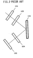
Here, circular polarisation modulation will be briefly described with reference to
Fig. 2. A linearly polarised beam having passed through a linear polariser 101 is given,
by a piezo-optical modulator 102 working on birefringence, an optical delay which
changes at a frequency of p (Hz). Then, the same beam, after having been reflected
from or passed through a sample 103 (the beam is reflected from the sample in Fig. 2),
is allowed to pass through an analyser 104 to reach a light receiving element 105 for
registration. From the p (Hz) component and 2p (Hz) component of the beam having
passed through the analyser 104, it is possible to determine the circular dichroism and
optical rotation the beam has undergone, respectively.
The principle underlying circular polarisation modulation will be described by
equations. For brevity, the direction along which a beam travels is assumed to coincide
with the z-axis. Assume that in Fig. 2 the linear polariser 101 has an angle of 45° with
respect to x-axis. The electric field E1 of the beam having passed through the linear
polariser 101 can be expressed by:
E1 α (i + j)
given that i and j are the unit vectors of x- and y-axes respectively.
Given that there is a delay of δ between x- and y- components of the electric field
E2 of the beam which has passed through the piezo-optical modulator 102,
E2 α {i + exp (i δ)j}
Assuming that the unit vectors of right- and left- circularly polarised beams are
expressed by the following equations respectively:
r = (i + ij) /2½
I = (i - ij)/2½
then, E2 can be expressed by the following equation:
E2 α {1-i.exp(iδ)) r + (1 + i.exp(i δ)) i}
Suppose that the complexly expressed amplitude reflections of right- and left-circulatory
polarised beams are expressed by r + exp (i +) and r - exp (i -)
respectively, then the electric field E3 of reflected beam can be expressed by:
E3 α {(1 - i.exp(iδ)) r + exp (i +) r + (1 + i.exp(i δ)) r. exp (i -)I}
The intensity I of the beam emanating from the analyser having an angle of with
respect to the x-axis is expressed by:
Iα {R + (ΔR/2)sin δ + R sin (Δ + 2) cos δ}
where
R = (r+2 + r-2)/2
ΔR = r+2 - r-2
Δ = + - - = -2k
ΔR/R = 4 ηk
and where k represents a Kerr's rotation angle and ηk a Kerr's ellipticity. Assuming
that = 0, and Δ is sufficiently small, δ ∼sin2 πpt. Then, the equation can be
resolved by the use of Bessel function into:
I∼I(0) + I(p) sin2πpt + I(2p) cos4πpt +
In this equation, I(o), I(p), and I(2p) represent factors respectively containing 0th-
order, 1st-order and 2nd order Bessel functions, and
I(p) α ηk, I(2p)α k
Therefore, the p(Hz) component gives the Kerr's ellipticity and the 2p (Hz) gives
the Kerr's rotation angle. For details, see the above-described "Light and magnetism."
The above-described various methods employed for the observation of minute
magnetic sectors have a number of problems as will be described. For example,
polarised light microscopy, operating in the same manner as conventional optical
microscopy, has its resolution restricted by the diffraction limit of the beam used, and
only achieves a resolution that allows detection to a width of about half the wavelength
of the beam used. Further, as it depends on the cross-Nichols method for detecting the
optical activities of a sample, its detection sensitivity is low. Lorenz transmission
electronmicroscopy has a resolution sufficiently high to distinguish about 10nm intervals,
but it is only applicable to a thinly sectioned sample. Spin-polarised scanning
electronmicroscopy has a problem in that it requires a large cost for instalment.
Magnetic force microscopy has a considerably high resolution that allows discrimination
of several tens of nm intervals, but it can scarcely be applied for the quantitative
determination of the magnitude of a magnetic field or magnetisation. The scanning near
field optical microscope has its resolution determined principally by the diameter of the
opening of the probe, and has a considerably high resolution. The conventional minute
spot scanning microscopy, however, usually depends for the detection of optical
activities of a sample, on the cross Nichols method, and presents the following problems.
It allows only a low sensitivity. Notwithstanding that the closer the minute spot beam
emanating from a minute opening is to a linearly polarised beam, the higher the detection
sensitivity, the minute spot beam emanating from a minute opening is usually elliptically
polarised. This may form another cause for lowered sensitivity.
Among the apparatuses for quantifying various magneto-optical effects, there are
some that allow the very sensitive quantification of a rotation angle through modulation,
for example, by the use of a rotating analyser. This method, however, can not be
applied to a tiny area exceeding the typical level handled by a conventional optical
microscope.
As illustrated above by referring to the microscopic observation of magneto-optical
effects as an example, the conventional methods whereby the distribution and
quantification of optical activities of a sample have been obtained have more or less
defects to be corrected, although some are advantageous in sensitivity, resolution and
tolerance of sample handling, and others are advantageous in cost. What is mentioned
above applies to the measurement not only of magneto-optical effects but also of optical
activities at large. In view of this the object of the present invention is to provide an
apparatus with which it is possible to observe/measure the optical activities of a sample
with a high resolution and sensitivity, at a low cost, quantitatively, and without imposing
any restrictions on the handling of the sample.
It is an object of the present invention to provide a scanning near field optical
microscope based on polarised light which requires only a low cost for production
because of its being based on the constitution of scanning atomic force microscopy, and
allows observation of a sample without imposing any restrictions on the preparation
thereof.
It is another object of the present invention to provide a scanning near field optical
microscope where the size of a beam to radiate a sample or emanating from a sample is
determined by the size of tip according to the principle underlying the scanning near field
optical microscope. Thus it allows the observation of a sample with a very high
resolution without being affected by a diffraction limit.
It is another object of the present invention to provide a scanning near field optical
microscope which can achieve a highly sensitive circularly polarised modulation by
giving a periodically changing optical delay to a beam.
It is a further object of the present invention to provide a scanning near field
optical microscope where it is possible to reduce the changes in polarisation state due to
external disturbing sources when the probe consists of a light transmitting body made of
a material having a smaller photo-elasticity coefficient, and it can minimise the adverse
effects due to stresses developed as a result of bending when the same material is applied
for the preparation of a probe with a hook-like shape.
According to a first aspect of the present invention there is provided a scanning
near field optical microscope comprising: a light source; a probe having a tip; means
operatively to maintain the interval between the tip and a sample surface or medium
within an action distance within which an interactive force results between the tip and the
surface; means to obtain a polarised beam carrying optical information concerning the
sample surface or medium, by allowing a beam from the light source to interact with the
surface adjacent the tip; light receiving means to receive the polarised beam; modulating
means placed in the light path between the light source and the light receiving means to
establish a periodically changing optical delay in the beam.
Preferably the probe is allowed to have a light transmitting body.
Preferably the means which maintains the tip so close to the surface of a sample
that the interval therebetween is kept within an action distance which allows and inter-atomic
interaction or interactions by way of other elements further comprises:
Preferably the distance determining means still further comprises:
Preferably the modulating means which is inserted on a light path between the
source and the light receiving means, and gives an optical delay changing at a regular
cycle acts as a means to generate a periodically changing stress in the light transmitting
body.
Preferably the present invention further comprises:
Preferably the material constituting the light transmitting body includes quartz
glass containing lead oxide.
Embodiments of the present invention will now be described by way of further
example only and with reference to the accompanying drawings, in which:
Fig. 1 is an explanatory view showing the constitution of Example 1 of a scanning
near field optical microscope based on polarised light according to this invention.
Fig. 2 is an explanatory view showing the constitution of element necessary for a
conventional method for measuring magneto-optical effects based on circular polarisation
modulation.
Fig. 3 is an explanatory view showing the constitution of Example 2 of a scanning
near field optical microscope based on polarised light according to this invention.
Fig. 4 is an explanatory view showing the constitution of Example 3 of a scanning
near field optical microscope based on polarised light according to this invention.
Fig. 5 is an explanatory view showing the constitution of Example 4 of a scanning
near field optical microscope based on polarised light according to this invention.
(1) Example 1
Fig. 1 illustrates the constitution of Example 1 of this invention. The basic
constitution is the same as that of a conventional scanning near field optical microscope.
The figure shows an apparatus which incorporates an optic fibre probe which is produced
after an optic fibre acting as a light transmitting body has a minute opening prepared at
its tip, wherein a minute spot beam emanating from the minute opening radiates a sample
(illumination mode) and the beam after passing through the sample is registered
(transmission type). Description will be given with reference to this example.
Firstly, a conventional minute spot scanning microscopy will be described with
regard to its constitution and operation. A light source 11, comprising a gas laser, solid
compound-based laser, or semiconductor-based laser, generates a light flux which passes
through a polarisation adjusting element 17 consisting of a wavelength plate, and a piezo-optical
modulator 10, to be incident, through the intervention of a fibre coupler 9, on the
input end of a fibre optic probe 1. The optic fibre probe 1 is usually made of a single
mode fibre, and its other end has its tip sharpened and circumference coated by a film
composed of a metal like gold or aluminum, such that the tip has a minute opening
whose diameter is equal to or less than the wavelength of the beam. The beam incident
on the input end of optical fibre probe 1 emanates from the minute opening as a minute
spot beam. The optic fibre may be made of a multi-mode fibre or a single hollow fibre,
instead of a single mode fibre. Further, the optical fibre probe 1 has a part close to the
tip bent like a letter L, and is attached on the surface of a piezo-electric element such as
a bimorph or a quartz vibrator. It is possible to operate the apparatus in an AFM mode,
or a dynamic mode often used in conjunction with scanning atomic force microscopy
(AFM), by vibrating the optical fibre probe 1 vertically with respect to a sample by
means of the piezo-electric element 18.
A sample 2 is placed on a piezo actuator 15 which can move along x-, y- and z-axis
directions, and a controller 16 controls the movement of the piezo actuator 15. the
controller, while maintaining constant the distance between the sample 2 and the tip of
the optical fibre probe 1, scans the beam over the sample 2 in x- and y-axis directions
using the piezo actuator 15. In this example, a method based on a device generally
called an optical lever is used for determining the distance between the sample 2 and the
tip of the optical fibre probe 1. This method consists of converging a beam emanating
from a laser source 12 onto the surface of a mirror placed close to the tip of the optical
fibre probe 1, of receiving the reflected beam with a bisected light receiving element 13,
and of determining the difference between the intensities of beams received by respective
bisected segments, thereby to monitor the vibration state (frequency, amplitude and
phase of the vibration) of the optical fibre probe 1. For example, when the optical fibre
probe 1 comes close to the sample 2, its vibration state undergoes a change in the
presence of forces resulting from inter-atomic interactions. Therefore, by adjusting the
movement of the piezo actuator 15 Along the z-axis direction in such a way as to allow
the optical fibre probe 1 to make a vibration with a constant amplitude, it is possible to
maintain constant the distance between the surface of sample 2 and the tip of the optical
fibre probe. Thus, while maintaining constant the distance between the sample 2 and the
tip of the optical fibre probe 1, it is possible, by scanning the beam over the sample, by
moving the piezo actuator 15 in x- and y-axis directions and by monitoring how much
the piezo actuator 15 moves along the z-axis direction, to obtain an image of the surface
texture of the sample 2.
As the tip of the optical fibre probe 1 is positioned close to the surface of sample 2,
the minute spot beam emanating from the minute opening transmits through the sample
2, is converged by a converging lens 3, has its path bent by a mirror 4, and passes
through an analyser 5 and filter 6 to be received by a light receiving element 7. The
filter 6 placed in front of the light receiving element 7 is to cut off the laser beam 12
which acts as one arm of the optical lever.
As the light source 11 usually consists of a laser source based on a gas or solid
molecule, it often happens that a linearly polarised beam impinges on the optical fibre
probe 1. But, the optical fibre probe 1 generally contains elements which may resolve
the polarisation state or retard the phase, of an incident beam, and thus the minute spot
beam emanating from the minute opening often suffers a degraded polarisation or
becomes an elliptically polarised beam, notwithstanding that the incident light is a
linearly polarised beam. When such a polarised beam is radiated upon the sample 2, and
its polarisation state is monitored by a cross-Nichols method, the overall sensitivity will
become low. To avoid such inconvenience, it is necessary to insert a wavelength plate
or compensation plate, that is, an agent to cause an appropriate retardation, on the
incident path of the optical fibre probe 1, thereby to adjust the polarisation state of
incident light. Through this procedure it is possible to obtain a minute spot beam with a
practically linear polarisation.
In spite of above fact, this invention adopts circular polarisation modulation
dependent on a cross-Nichols method which is principally very sensitive. The method
adopted in this example whereby an optical delay is given to a minute spot beam
emanating from the minute opening of optical fibre probe 1 in accordance with a
modulation frequency p (Hz) depends on the use of a piezo-optical modulator (PEM) 10
working on birefringence which incorporates an optically active crystal such as quartz or
the like. A drive 14 to drive the PEM not only activates the piezo-optical modulator 10
but delivers a reference signal with respect to which a lock-in amplifier 8 performs a
lock-in rectification. A light flux emanating from the light source 11 passes through the
piezo-optical modulator 10 to be given an optical delay there, and is incident through the
intervention of fibre coupler 9 on the input end of the optical fibre probe 1.
Detection of optical activities using a modulated circularly polarised beam is so
sensitive that, as long as any optical delay is given at all to a minute spot beam by detect
optical activities. What should be noted here is that as long as the piezo-optical
modulator 10 incorporates an optically active crystal, the crystal axis should be taken
into account. Namely, modulation efficiency will be higher if an incident polarised
beam is adjusted according to the angle the beam forms with the axis of crystal. Thus,
the polarised state of an incident beam is adjusted by means of a polarisation adjusting
element 17 placed on the input side of the piezo-optical modulator 10. Needless to say,
the polarisation adjusting element 17 may be so constituted as to allow an incident beam
to pass through a half wavelength plate capable of rotating the beam, or to allow an
incident beam to pass through a quarter wavelength plate to convert it into a circularly
polarised beam, and then to permit a specific component thereof, say, a linearly
polarised beam to exit therefrom. This example uses a piezo-optical modulator 10
incorporating an optically active crystal, but any other modulator can be used with the
same advantage as long as it can give a periodic optical delay to an incident beam.
Placement of the mirror 4 in front of the analyser 5 is undesirable because the
mirror may add an extra polarisation characteristic, and ideally the light path should not
be bent. However, for a beam converged by the converging lens 4 to be guided to the
light receiving element 7, it is necessary with a conventional transmission type scanning
near field optical microscope to bend the light path by means of the mirror 4 for design
convenience. The mirror incorporates a dichroic mirror instead of a conventional
vapour-deposited aluminum mirror, thereby to lessen the difference in reflection of p-
and s-polarised beams. Through this procedure it becomes possible to ignore the
polarisation characteristic given by the mirror 4.
By virtue of an apparatus having the above constitution, a minute spot beam
emanating from the minute opening interacts with the surface of sample 2, is converted,
through that interaction, into a transmissive beam, passes through the sample 2 being
given, during passage, optical activities including circular dichroism and optical rotation,
and passes through the analyser 5 to be incident on the light receiving element 7 so that it
may be registered there. This signal is rectified by the lock-in amplifier 8 which uses the
reference signal (having a frequency of p) delivered by the PEM driver 14 for
rectification, and the rectified output is fed to the controller 16. When the 2p component
is submitted to lock-in rectification, it gives an optical rotation, and when the p
component is submitted to lock-in rectification, it gives a circular dichroism. Thus,
when these signals are submitted to the controller 16 to be converted into images in
synchrony with the scanning movement of the piezo actuator 15 as in a conventional
scanning near field optical microscope, they will visualise the distribution of optical
activities of the sample. Incidentally, if only the p component is required, the analyser 5
placed in front of the light receiving element 7 may be omitted.
Further, when not only the distribution of optical activities but also the absolute
quantities of those activities are desired to be measured the ratio of the p component to
the direct current component will give the ellipticity and the ratio of the 2p component to
the direct current component will give the optical rotation. For the latter purpose it is
not necessary to move the piezo actuator 15 so that the beam can scan over the sample
along x- and y-axis directions, but to adjust the piezo actuator 15 such that a desired spot
of sample 2 is placed close to the optical fibre probe 1 for measurement. By this process
it is possible to quantitatively determine the optical activities of a very tiny area of a
sample as with a conventional method based on the modulation of a circularly polarised
beam.
Assuming that the optical fibre probe 1 gives an optical delay of π/2 as a result of
mechanical stresses as does a quarter wavelength plate, the electric field E2 of a beam as
described by equation (2) above comes to be expressed by the following equation
because of an optical delay given by the optical fibre probe 1.
Ex α {i + i.exp (iδ)j}
As a result, the intensity I of light emanating from the analyser becomes:
I α {R + (ΔR/2)cos δ + R.sin (Δ + 2 ) sin δ}
This equation, when resolved by a Bessel function, gives:
I ∼ I(0) + I(p) sin2πpt + I (2p) cos 4π pt +
I(p) α k, I(2p) α ηk
What is worthy of notice here is that what the p and 2p components represent in
this equation is opposite to what the same components expressed in equation (7) above
represent.
The present invention can have the above-described constitution and operate in the
above-described manner, and combines a scanning near field optical microscope with
circular polarisation modulation thereby to make it possible not only to observe the
distribution of optical activities of the sample 2 with a high sensitivity and resolution, but
also to quantitatively determine the optical rotation and ellipticity of a specified tiny area
of the sample. Further, as this method is based on a scanning near field optical
microscope, it allows the production of a smaller apparatus with a lower cost than is
possible with other similar observation means dependent on conventional techniques.
The sample 2 may be in the atmosphere, in a liquid, or in a vacuum for measurement,
and does not need to be thinly sectioned. Thus, this method does not impose any special
restrictions on the preparation of the sample.
(2) Example 2
Next, Example 2 according to this invention will be described with reference to
Fig. 3 which shows the constitution of Example 2 of this invention. In Example 1 light
is passed through a sample for measurement. In example 2 measurement is performed
using light reflected from a sample. As the basic constitution and operation are the same
as those of Example 1, parts achieving the same functions are represented by the same
symbols, and their detailed explanation will be omitted.
The process the beam undergoes, after having emanated from the light source 11,
till it exists from the minute opening of the optical fibre probe 1 as a minute spot beam
are practically the same as that of the beam in Example 1. However, in example 2, a
piezo-optical modulator 10 is not placed on a light path between the light source 11 and
the optical fibre probe 1. As described above, the optical fibre probe 1 often has the
property of retarding a beam. This is especially true when the optical fibre probe 1 is
bent like a letter L so as to be operable in a dynamic AFM mode because the bent part
causes a retardation in the beam. To avoid such inconvenience, a polarisation adjusting
element 17 is paced on the input side of optical fibre probe 1 and the polarisation state of
an incident beam is modified by that polarisation adjusting element 17 so as to adjust the
polarisation characteristics of the minute spot beam emanating from the minute opening.
The polarisation adjusting element 17 usually consists of a wavelength plate like a half-wavelength
plate or a quarter-wavelength plate, but he use of a compensatory plate will
allow a more precise adjustment.
A minute spot beam reflected from the sample 2 after having interacted with the
latter is converged by a converging lens 3. The converging lens 2 may be positioned at
any place on the light path as long as it efficiently converges the minute spot beam
reflected from the sample 2, or, instead of being made of a lens, it may be made of a
light-converging mirror like a parabolic mirror, as long as it has a light converging
activity. The beam, after being converged by the converging lens 3, is given an optical
delay with a frequency of p (Hz) while it passes through a piezo-optical modulator 10,
and then passes through an analyser 5 and filter 6 to be received by a light receiving
element 7. As far as only the determination of circular dichroism of a beam from the p
component is required, the use of analyser 5 may be omitted. As the remaining
constitutions and operations are the same as those of Example 1, description of them will
be omitted. Also with example 2 one can visualise the distribution of optical activities of
sample 2 and quantitatively determine those optical activities with a high sensitivity and
resolution.
Although in Example 1 the piezo-optical modulator 10 is placed on the input side
of optical fibre probe 1, it is needless to say, the device in question may be put between
the analyser 5 and sample 2 as in example 2. However, as the piezo-optical modulator
10 usually incorporates an optically active crystal, it is possible to efficiently give an
optical delay to an incoming beam by directing the beam to the modulator 10 such that
the polarisation plane of the beam has a specific angle with respect to the crystal axis. If
the piezo-optical modulator 10 is positioned in such a way as to receive light reflected
from the sample 2, the polarisation plane of the light will not take an optimum angle
with respect to the crystal axis, and thus the modulation efficiency and detection
sensitivity will often be worsened and lowered.
(3) Example 3
Next, Example 3 according to this invention will be described with reference to
Fig. 4 which illustrates the constitution of Example 3 of this invention. Although in
Examples 1 and 2 an illumination mode is adopted whereby a beam emanating from a
minute opening is allowed to illumine a sample, in example 3 a collection mode is
adopted whereby a minute spot beam is detected through a minute opening. Further, a
beam is allowed to pass through the sample 2. Parts having the same constitution or
achieving the same functions as the corresponding parts of Example 1 are represented by
the same symbols, and their explanation will be omitted.
A beam emanating from a light source 11 is given an optical delay during passage
through a polarisation adjusting element 17 and piezo-optical modulator 10, and this is
the same as in Example 1. The beam, after having been given an optical delay, is
converged by a converging lens 19 into a convergent beam, and is incident through a
side wall onto a triangular prism 21 carrying a sample 2 and converged to the bottom
surface thereof. When the incident angle of the converged beam with respect to the
bottom surface of the prism exceeds a critical angle, that beam is totally reflected by that
bottom surface, and the side of the bottom surface facing the sample 2 gives rise to an
evanescent beam. When an optical fibre probe having a minute opening at its tip is
allowed to approach the sample 2 by the same method as used in Example 1, the
evanescent beam present on the surface of sample 2, through interaction with the optical
fibre probe 1, is converted into a transmissive beam which enters into the minute
opening, transmits through the optical fibre probe 1, and exits from the other end of the
same probe. The beam emanating from the other end of probe is collimated by a
collimator 20, and is allowed to pass through an analyser 5 and filter 6 to be received by
a light receiving element 7. As the constitution of other elements and their operation are
the same as those of Example 1, their explanation will be omitted. With example 3, it is
also possible to obtain the distribution of optical activities of sample 2 or to
quantitatively determine the optical activities thereof with a high sensitivity and
resolution.
Example 3 uses the triangular prism 21 in such a way as to totally reflect an
incident beam to produce an evanescent beam, but the total reflection may be produced
by means of a dark-field illumination and, needless to say, the method is not limited to
any specific one as long as an evanescent beam is produced on the surface of sample 2.
It is also needless to say that, as in Example 1, the optical fibre probe 1 is allowed to
illumine a tiny are of sample 2, and to receive a beam having undergone an interaction
for measurement. In this case, the optical fibre probe must have, at the other end, a
beam separating element like a beam splitter which separates a beam into an illumination
component and a detection component.
In Examples 1, 2 and 3 described above, the optical fibre probe 1 has a minute
opening at its tip, and radiates or transmits a minute spot beam through the minute
opening for radiation or for measurement. It is needless to say, however the probe is not
limited to any specific one. Preferably, it has a light transmitting body acting as a wave
guide channel, being made of a comparatively transparent material to the wavelength of
beams often used for measurement, like quartz or lithium niobate, and has a minute
opening at its tip which is equal or less in size than the wavelength of the beam.
In Examples 1, 2 and 3 described above, the piezo-optical modulator 10 is
installed, besides the optical fibre probe 1, to give an optical delay. However, many of
the above-described light transmitting bodies can give an optical delay through photoelasticity
effects in the presence of an external force. Namely, instead of the piezo-optical
modulator 10, a periodic force may be applied to a part of light transmitting body
of the probe, and the resulting photo-elasticity effects may be utilised to give an optical
delay changing in a periodic manner to a beam during the passage of the beam through
the light transmitting body. Further, by adjusting the intensity of the external force, it is
possible to alter the magnitude of the optical delay. As a result, it is possible to reduce
the overall size of the apparatus.
Further, the method whereby th polarisation state of a minute spot beam is adjusted
by a polarisation adjusting element 17 placed on the input side of a probe consisting of a
light transmitting body is effective for the measurement combined not only with the
modulation of a circularly polarised beam, but also with a cross-Nichols method. For
example, although the optical fibre probe 1 may be bent in a form like a letter L so that
the distance between the optical fibre probe 1 and sample 2 may be dynamically changed
according to a dynamic AFM mode, the optic fibre probe 1 will then present an optical
anisotropy which causes a retardation in a beam passing there through. As a result, even
if a linearly polarised beam is fed to the optical fibre probe 1, only an elliptically
polarised beam will emanate from the minute opening. This inconvenience can be
avoided by inserting a polarisation adjusting element 17 in such a way as to cancel out
the retardation, thereby allowing the minute spot beam to approximate to a linearly
polarised beam. Therefore, when this arrangement is applied to a cross-Nichols method,
the overall detection sensitivity will become higher than is possible with a similar
apparatus dependent on the cross-Nichols method which uses an elliptically polarised
beam emanating from the minute opening without any special treatment therefor.
In the above-described examples, the polarisation adjusting element 17 is installed,
besides the optical fibre probe 1, to change the polarisation state of a beam before the
beam is incident on the optical fibre probe 1. It is needless to say, however, that when a
method is employed which consists of directly applying a force onto part of the optical
fibre probe 1 and of controlling the intensity of that force, it is possible to alter the
polarisation state of a beam during its passage through the optical fibre by way of photoelasticity
effects resulting from the external force, thus allowing the optical fibre probe 1
also to act as a polarisation adjusting element 17.
A typical glass material has a photo-elasticity coefficient of about 2-4 (10-6mm2.N-6),
and stresses therein cause a retardation in a beam passing there through.
Hence a beam passing through such a glass material undergoes a change in its polarised
state. This can occur in the optical fibre probe 1 of Examples 1, 2 and 3 described
above. When the optical fibre (particularly its core section ) acting as a light
transmitting body is exposed to a vibration externally applied, or vibrates itself while
securely fixed, so that stresses develop within the fibre; a beam passing there through has
its polarisation state altered as a result of photo-elasticity effects. The eternal vibration
acts as a noise source to lower the S/N ratio, or only a slight shift of fixation may
destroy the reproducibility of measurements. When the distance between the optical
fibre probe 1 and sample 2 is controlled according to a dynamic AFM mode, the optic
fibre probe 1 must be bent like a hook as with an AFM cantilever. To take such a form
the fibre has to be bent while being heated, and the bent part has residual stresses. When
a beam passes through this part, it receives an optical delay as a result of photo-elasticity
effects. This not only applies to a part bent in the form of a hook, but also to the general
form of an optical fibre probe 1 which is often not symmetrically configured with respect
to the axis of light transmission, which results in the development of residual stresses.
To meet the above inconvenience, a probe is prepared whose light transmitting
body is made of a material having a photo-elasticity coefficient of 1 x 10⁻⁶ (mm2.N-6)
or less. By preparing such a probe it is possible to ignore the effects of stresses caused
by external vibrations and fixations, and to suppress the effects of residual stresses
developing as a result of asymmetrical configuration with respect to the optical axis to a
negligible level. For example, crown glass FK51 or FK52 provided by Shot Co. has a
photo-elasticity coefficient of about 0.7-1 x 10⁻⁶ (mm2.N-6). Further, flint glass SF57
provided by Shot Co. which is composed of quartz containing a large amount of lead
oxide has a photo-elasticity coefficient of about 0.02 x 10⁻⁶ (mm2.N-6). It can have a
coefficient as small as 0.005 x 10⁻⁶ (mm2.N-6), depending on the ingredients contained
therein. It is also possible to prepare an optical fibre probe from these glass materials.
Thus, a light transmitting body made of a material whose photo-elasticity coefficient is 1
x 10-6 (mm2.N-6) or less is utilised to form a probe, and with that probe it is possible to
make a measurement where changes in polarisation characteristics due to external
vibrations are effectively suppressed and a satisfactory S/N radio is maintained. Further,
even when the optical fibre probe 1 has its stem bent like a hook as in Examples 1, 2 and
3, it is possible to greatly reduce the changes in polarisation state which otherwise a
beam would have suffered during passage through the bent part. As is evident from the
above, preparing a probe from a light transmitting body made of a material having a
smaller photo-elasticity coefficient is very useful for a measurement dependent on the use
of a polarised beam including a cross-Nichols method as well as circular polarisation
modulation.
Incidentally, without resorting to the preparation of a probe from a light
transmitting body made of a material having a smaller photo-elasticity coefficient, it is
possible to suppress the effects of residual stresses which may develop during the
preparation of the probe by annealing the light transmitting body.
(4) Example 4
In Examples 1 to 3, the light transmitting body consists of an optical fibre which
has its tip sharpened, and has a minute opening at the probe tip. However, the method
of illuminating a tiny area of a sample by a beam emanating from the tip of probe is not
limited to radiation through a minute opening. There are a number of variants: an
evanescent beam can be produced by plasmon deposited on the surface of a minute ball,
or a grating whose lattice pitch is so shortened that the diffraction angle is lost. Further,
the method whereby the tip of the probe can detect a beam emanating from a tiny area of
the sample also has a number of variants: an evanescent beam may be produced on the
surface of a sample by total reflection or by reflection from a surface-coated plasmon.
Besides the above a method may be employed whereby a cantilever, instead of a
light transmitting body, which is produced after a semiconductor such as silicone or a
metal has been sharpened, is utilised as a probe. Then, for example, the surface of the
sample and the sharpened tip of the probe are illumined by dark-field illumination as
often used in microscopy; to cause a multiple scattering to occur between the sample and
cantilever tip, and the scattered beam is measured by an external optical system.
Next, Example 4 of this invention wherein the probe does not consist of a light
transmitting body will be described with reference to Fig. 5 which shows the constitution
of Example 4 of this invention. A probe 22 may consist of a metal probe as used in a
scanning tunnel microscope or a silicone cantilever as used in a scanning atomic force
microscope, or other various materials. But, needless to say, it is not limited to any
specific materials as long as the material has a high scattering efficiency. The sharpened
tip of probe 22 is allowed to get close to a sample 2. The example depicted in the figure
uses an optical lever to move the tip towards the sample, and as this tool is the same as
those described earlier, explanation thereof will be omitted. The sample 2 is placed on a
piezo actuator 15 and moves in x-, y- and z-axis directions.
A light flux emanating from a light source 11, after having passed through a
polarisation adjusting element 17 and piezo-optical modulator 10, is converged by a
collimator 20 and illumines the sample 2 and the tip of the probe 22. This illuminating
beam is given a periodically changing optical delay through the piezo-optical modulator
10. The light source 11 is usually a laser, and there is no element in the light path that
may disturb the polarisation state of the beam passing along a light path such as the
optical fibre probe as encountered in foregoing examples, but the polarisation adjusting
element 17 is used to adjust the polarisation direction of an illuminating beam according
to the condition of the sample 2.
As the tip of the probe 22 gets so close to the sample 22 that the distance
therebetween is equal to or less than the wavelength of the illuminating beam, a multiple
scattering takes place as a result of interaction between the surface of the sample 2 and
the tip. This multiply scattered beam carries optical information regarding the surface
condition of the sample 2 depending on the size of the tip of the probe 22. A converging
lens converges this scattered beam which is then passed through an analyser 5 and filter 6
to be received by a light receiving element 7. As the subsequent processes are the same
as those of foregoing examples, explanation thereof will be omitted. Adjusting the
angles of light source 11 and of light receiving element 7 with respect to the sample 2, so
that a beam emanating from the light source 11 to illumine the sample 2 and the probe
22 may not enter the light receiving element, will enable a selective pick-up of a
multiply scattered beam, and achievement of a measurement with a satisfactory S/N
ratio. As is evident from the above, even if a probe does not consist of a light
transmitting body, it is possible to constitute a scanning near field optical microscope
based on circular polarisation modulation, and to observe optical activities of a sample
with a high sensitivity.
When a beam from the light source 11 radiates from one direction onto the sample
2 as in Fig. 5, entry of the radiating beam from the light source 11 into the light
receiving element 7 should be avoided as much as possible. Further, this example is
based on a transmission type apparatus, but what is mentioned above also applies to a
reflection type apparatus.
Examples 1 to 4 described above use an optical lever to detect the displacement of
the optical fibre probe 1 or the probe 22. However, the method is not limited to an
optical lever or any other specific methods, as long as the method permits detection of
the minute displacement of the optical fibre probe 1 or the probe 22. For example, when
a dynamic AFM mode is employed, the probe may be applied on a quartz vibration
detector, and the changes in vibration of the probe be followed by voltages delivered
from the quartz vibration detector being monitored.
In Examples 1 to 4 described above, the method of controlling the distance
between the optical fibre probe 1 or the probe 22 and the sample 2 is based on a dynamic
AFM mode. However, the method is not limited to any specific modes, as long as the
distance between the optical fibre probe 1 or the probe 22 and the sample 2 can be
rendered to any small size at will: the distance in question may be adjusted according to
a static AFM mode, or by light interference, or on the basis of a shearing force produced
as a result of interaction between the two elements here concerned, or through the
utilisation of a tunnel current. If the latter method is used, the optical fibre probe 1 or
the probe 22 need not be bent like a letter L.
Although in Examples 1 to 4 described above, the distance between the optical
fibre probe 1 or the probe 22 and the sample 2 is measured and actively controlled on
the basis of the measurement, the method is not limited to this. For example, the probe
and sample may be allowed to move relative to each other to cause a current to flow
therebetween, thereby maintaining constant the distance between the probe and sample
surface by virtue of the viscosity of fluid as in a hard disk drive where the magnetic head
floats by a certain definite amount (e.g., about 100nm) over the disk by virtue of an air
bearing. Thus, the method does not necessarily require measurement of the distance
between the probe and sample surface and a continuous monitoring of the proximity of
the two elements here concerned. But, any method can be used with the same result as
long as it allows the probe and sample surface to be close and constant to each other.
In Examples 1 to 4 described above, the light source 11 generates a laser beam
composed of a single wavelength. However, a Xenon lamp may be used as the light
source 11, and light therefrom may be used after it has passed through a spectroscope so
that an appropriate component might be selected. In this case, measurement can be
performed using beams with different wavelengths.