EP0877339A2 - Spatial non-uniformity correction of a color sensor - Google Patents

Spatial non-uniformity correction of a color sensor Download PDF

Info

Publication number
EP0877339A2
EP0877339A2 EP98201328A EP98201328A EP0877339A2 EP 0877339 A2 EP0877339 A2 EP 0877339A2 EP 98201328 A EP98201328 A EP 98201328A EP 98201328 A EP98201328 A EP 98201328A EP 0877339 A2 EP0877339 A2 EP 0877339A2
Authority
EP
European Patent Office
Prior art keywords
color
matrix
monocolor
colors
quad
Prior art date
Legal status (The legal status is an assumption and is not a legal conclusion. Google has not performed a legal analysis and makes no representation as to the accuracy of the status listed.)
Withdrawn
Application number
EP98201328A
Other languages
German (de)
French (fr)
Other versions
EP0877339A3 (en
Inventor
Andrew Setsu C/O Eastman Kodak Company Katayama
Current Assignee (The listed assignees may be inaccurate. Google has not performed a legal analysis and makes no representation or warranty as to the accuracy of the list.)
Eastman Kodak Co
Original Assignee
Eastman Kodak Co
Priority date (The priority date is an assumption and is not a legal conclusion. Google has not performed a legal analysis and makes no representation as to the accuracy of the date listed.)
Filing date
Publication date
Application filed by Eastman Kodak Co filed Critical Eastman Kodak Co
Publication of EP0877339A2 publication Critical patent/EP0877339A2/en
Publication of EP0877339A3 publication Critical patent/EP0877339A3/en
Withdrawn legal-status Critical Current

Links

Images

Classifications

    • GPHYSICS
    • G06COMPUTING; CALCULATING OR COUNTING
    • G06TIMAGE DATA PROCESSING OR GENERATION, IN GENERAL
    • G06T5/00Image enhancement or restoration
    • G06T5/20Image enhancement or restoration by the use of local operators

Definitions

  • This invention relates in general to image processing and relates more particularly to the correction of spatial non-uniformities of an image produced by a color image sensor.
  • CFA color-filter-array
  • the sources of the non-uniformities is due to at least two mechanisms: non-uniformities in the poly-oxide sensor layer, resulting in a spatially varying spectral response, and the non-uniform application of the dyes when they are spun onto the die.
  • the behavior of these non-uniformities is such that they are slowly varying. It has been found that a quadratic model provides an accurate enough of a fit to the actual non-uniformity profile.
  • a color imaging system comprising a color image sensor having a matrix of photosites and a color filter array (CFA) masking the matrix of photosites, such that each photosite captures one color of first, second, and third colors, the CFA constituting a repetitive pattern of the first, second and third colors, the sensor producing a color image signal including a matrix of monocolor pixels corresponding to the color filter array pattern; and a field programmable gate array which is programmed as a spatial non-uniformity color corrector for correcting each of the monocolor pixels of the color image signal by a simplified quadratic function along each image axis.
  • CFA color filter array
  • Fig. 1 is a block diagram of a color image system incorporating the present invention.
  • Fig. 2 is a diagrammatic view of a CFA color image sensor.
  • Fig. 3 is a conceptual block diagram of an implementation of the present invention.
  • Figs. 4-6 are degenerative block diagrams of Fig. 3 useful in explaining the present invention.
  • color imaging system 10 includes a color video camera 12, color image processor 14, and color image display 16.
  • Color video camera 12 includes a lens 18, CCD color image sensor 20, correlated double sampling (CDS) circuit 22, analog-to-digital converter (A/D) 24, high speed serial link driver 26, central processing unit (CPU) 28 and memory 30.
  • Color image processor 14 includes high speed serial link driver 32 (linked to driver 26 by high speed link 27), frame store 34, uniformity corrector 36, color interpolator 38, CPU 40, timing generator 42, and digital-to-analog converter (D/A) 44.
  • Display 16 can be any type of video display, such as CRT, LCD, plasma.
  • Color imaging system 10 operates as follows. A scene to be captured is projected on sensor 20 by lens 18. Sensor 20 produces an analog video signal which is noise corrected by CDS circuit 22. A/D 24 converts the analog video signal to a digital video signal which is transmitted to processor 14 by high speed link 26. Memory 30 stores spatial non-uniformity correction data unique to sensor 20 which is used in the spatial non-uniformity correction technique of the present invention. Camera CPU 28 transmits this data to processor CPU 40 over a serial link 46.
  • Color image processor 14 receives the digital image data by means of link 27 and stores it in frame store 34.
  • the digital image data is corrected for spatial non-uniformities by a correction algorithm implemented in a field-programmable gate array which includes corrector 36.
  • Corrector 36 includes three correctors, one for each color R,G,B.
  • each monocolor pixel is color interpolated by color interpolator 38 to produce an RGB tri-color pixel.
  • the digital color image is converted by D/A 44 to an analog color image which is displayed on display 16.
  • CPU 40 and timing generator 42 provide correction coefficient data and timing signals to corrector 36.
  • Sensor 20 is a CCD sensor having a color filter array over the CCD pixel sites.
  • One color component is captured per pixel.
  • interpolation is required to construct three full RGB color planes for the image.
  • An exemplary color filter array pattern is shown in Fig. 2 for a 1023 ⁇ 1535 pixel active image area.
  • the CFA consists of a regular 2 ⁇ 2 pixel array of kernels.
  • Each kernel 50 consists of two green pixels 52,54 on one diagonal and a red pixel 56 and blue pixel 58 on the other diagonal.
  • each monocolor pixel is corrected for spatial non-uniformity by corrector 36 which has separate correctors for each color R,G,B.
  • corrector 36 which has separate correctors for each color R,G,B.
  • f approx ( x , y ) f approx_x ( x ) + f approx_y ( y ) + ( c + C -1)
  • f approx_x ( x ) a ⁇ x 2 + b ⁇ x
  • f approx_y ( y ) A ⁇ y 2 + B ⁇ y
  • corrector 36 includes addressable scratchpad registers 60,62,64,66, addressable coefficient registers 68,70,72,74,76 adders 78,80, multiplexers 82,84,86,88,90,92,94.
  • the inputs and outputs to the corrector are marked with ellipses in the drawing.
  • the inputs consists of two 1-bit inputs, one input 100 marks the first pixels of a frame for the current color component, and the other input 102 which marks the first pixel of the line for the current color component.
  • the current color component being accessed is indicated by the input 104 referred to as "current color component index".
  • this may be implemented as a 2-bit input.
  • the fourth input is the configuration interface 106, which is used to upload the five parameters for each of the color component profiles to be generated on output 108.
  • output 108 outputs the value of the quadratic surface for the current pixel.
  • Inputs 100,102 are generated by timing generator 42, input 104 is coupled to frame store 34 and input 106 is coupled to CPU 40.
  • the mode shown in Fig. 5 takes us through the execution of the innermost "for" loop in the pseudo-code.
  • quad ( x , y ) and quad ⁇ x ( x +1, y ) are enabled for update via their respective write enable (wen) controls.
  • wen write enable
  • both of these quantities are being incremented by the quantities quad ⁇ x ( x +1, y ) and 2 ⁇ a, respectively, thus implementing the innermost "for" loop.

Abstract

A color imaging system comprising a color image sensor having a matrix of photosites and a color filter array (CFA) masking the matrix of photosites, such that each photosite captures one color of first, second, and third colors, the CFA constituting a repetitive pattern of the first, second and third colors, the sensor producing a color image signal including a matrix of monocolor pixels corresponding to the color filter array pattern; and a field programmable gate array which is programmed as a spatial non-uniformity color corrector for correcting each of the monocolor pixels of the color image signal by a simplified quadratic function along each image axis.

Description

FIELD OF THE INVENTION
This invention relates in general to image processing and relates more particularly to the correction of spatial non-uniformities of an image produced by a color image sensor.
BACKGROUND OF THE INVENTION
The need for uniformity correction to correct for hue shifts in a single color-filter-array (CFA) image sensor has been recognized. Such sensors uses a regular pattern of colored dyes directly over the pixel sites in order to capture one color component per pixel. One particular pattern used in a digital still camera consists of a regular 2 × 2 pixel array of kernels. Each kernel consists of two green pixels on one diagonal, and one each of a red and blue pixel on the other diagonal. In order to reconstruct a full RGB (red, green, blue) image, processing is required to reconstruct the missing color information at each pixel site.
The sources of the non-uniformities is due to at least two mechanisms: non-uniformities in the poly-oxide sensor layer, resulting in a spatially varying spectral response, and the non-uniform application of the dyes when they are spun onto the die. The behavior of these non-uniformities is such that they are slowly varying. It has been found that a quadratic model provides an accurate enough of a fit to the actual non-uniformity profile.
When the digital image from a CFA digital camera is transferred to a computer, all spatial and colorimetric processing is done by software on the host computer, as the application does not demand real-time processing. Included in this processing is an algorithm to correct the red and blue color planes for non-uniformities. As these corrections are performed in software by the host computer, multiplications are left in the implementation of the algorithm.
There is a need to correct spatial non-uniformities in a video rate (as opposed to still-frame) color imager, where we wish to process the color information in real-time to be able to support a live color display output. Thus, the processing needs to be performed in real-time. It is therefore essential in such an application to reduce the costs of the implementation such that they can be implemented economically in off-the-shelf components.
SUMMARY OF THE INVENTION
According to the present invention, there is provided a solution to the needs discussed above.
According to an aspect of the present invention, there is provided a color imaging system comprising a color image sensor having a matrix of photosites and a color filter array (CFA) masking the matrix of photosites, such that each photosite captures one color of first, second, and third colors, the CFA constituting a repetitive pattern of the first, second and third colors, the sensor producing a color image signal including a matrix of monocolor pixels corresponding to the color filter array pattern; and a field programmable gate array which is programmed as a spatial non-uniformity color corrector for correcting each of the monocolor pixels of the color image signal by a simplified quadratic function along each image axis.
ADVANTAGEOUS EFFECT OF THE INVENTION
The present invention has the following advantages:
  • 1. Correction of spatial non-uniformities in a CFA color image sensor is done in real time at video rates to support a live color display output.
  • 2. The correction technique is implemented economically in off-the-shelf components.
  • BRIEF DESCRIPTION OF THE DRAWINGS
    Fig. 1 is a block diagram of a color image system incorporating the present invention.
    Fig. 2 is a diagrammatic view of a CFA color image sensor.
    Fig. 3 is a conceptual block diagram of an implementation of the present invention.
    Figs. 4-6 are degenerative block diagrams of Fig. 3 useful in explaining the present invention.
    DETAILED DESCRIPTION OF THE INVENTION
    Referring now to Fig. 1, there is shown a color imaging system incorporating the present invention. As shown, color imaging system 10 includes a color video camera 12, color image processor 14, and color image display 16. Color video camera 12 includes a lens 18, CCD color image sensor 20, correlated double sampling (CDS) circuit 22, analog-to-digital converter (A/D) 24, high speed serial link driver 26, central processing unit (CPU) 28 and memory 30. Color image processor 14 includes high speed serial link driver 32 (linked to driver 26 by high speed link 27), frame store 34, uniformity corrector 36, color interpolator 38, CPU 40, timing generator 42, and digital-to-analog converter (D/A) 44. Display 16 can be any type of video display, such as CRT, LCD, plasma.
    Color imaging system 10 operates as follows. A scene to be captured is projected on sensor 20 by lens 18. Sensor 20 produces an analog video signal which is noise corrected by CDS circuit 22. A/D 24 converts the analog video signal to a digital video signal which is transmitted to processor 14 by high speed link 26. Memory 30 stores spatial non-uniformity correction data unique to sensor 20 which is used in the spatial non-uniformity correction technique of the present invention. Camera CPU 28 transmits this data to processor CPU 40 over a serial link 46.
    Color image processor 14 receives the digital image data by means of link 27 and stores it in frame store 34. According to the present invention, the digital image data is corrected for spatial non-uniformities by a correction algorithm implemented in a field-programmable gate array which includes corrector 36. Corrector 36 includes three correctors, one for each color R,G,B. After spatial non-uniformity correction, each monocolor pixel is color interpolated by color interpolator 38 to produce an RGB tri-color pixel. The digital color image is converted by D/A 44 to an analog color image which is displayed on display 16. CPU 40 and timing generator 42 provide correction coefficient data and timing signals to corrector 36.
    Sensor 20 is a CCD sensor having a color filter array over the CCD pixel sites. One color component is captured per pixel. Thus, interpolation is required to construct three full RGB color planes for the image. An exemplary color filter array pattern is shown in Fig. 2 for a 1023 × 1535 pixel active image area. The CFA consists of a regular 2 × 2 pixel array of kernels. Each kernel 50 consists of two green pixels 52,54 on one diagonal and a red pixel 56 and blue pixel 58 on the other diagonal.
    According to the present invention, each monocolor pixel is corrected for spatial non-uniformity by corrector 36 which has separate correctors for each color R,G,B. The preferred correction algorithm will now be described.
    We wish to correct for spatial non-uniformities encountered in a large-array sensor. We will study a possible implementation to correct for spatially correlated multiplicative non-uniformities which can be approximated by a quadratic function along each image axis. Let us represent these multiplicative non-uniformities by the following function: f(x,y) = (a · x 2 + b · x + c) · (A · y 2 + B · y + C)
    However, as we expect that the surface features that we will be correcting for will be small, we can immediately simplify this relation by the binomial expansion as follows: (1 + Δx) · (1 + Δy) = 1 + Δx + Δy + Δx · Δy ≈ (1 + Δx) + (1 + Δy)-1 for small Δx, Δy
    Thus, we will now work with a simplified version of our original function in the following form: fapprox (x,y) = (a · x2 + b · x + c) + (A · y 2 + B · y + C)-1 = (a · x 2 + b · x) + (A · y 2 + B · y) + (c + C - 1) This is separable with respect to the variables x and y as follows: fapprox (x,y) = fapprox_x (x) + fapprox_y (y) + (c+C-1)    where: fapprox_x (x) = a · x 2 + b · x    and: fapprox_y (y) = A · y 2 + B · y We can now differentiate with respect to x and y as follows: ∂x fapprox_x (x) = 2 · a · x + b    and: ∂y fapprox_y (y) = 2 · A · y + B By differentiating once more with respect to x and y we obtain: 2 2 y fapprox_y (y) = 2 · A We can thus reconstruct the original functions as follows: fapprox (x,y) = fapprox_x (x) + fapprox_y (y) + (c + C - 1) = x min x max x min x max 2 · a · ∂ x + b x + y min y max y min y max 2 · A · ∂ y + B ∂ y + (c + C -1)
    We have now reduced the original function into a form which only involves the double-integration of constant terms. We thus have a form which can be implemented without any costly multiplications. What we will actually implement is a finite difference implementation of the above.
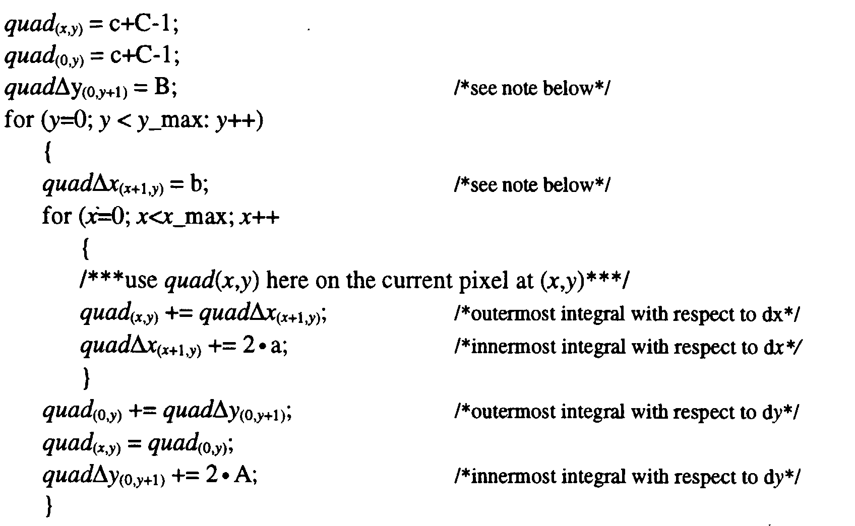
    Let us now define a few variables which we will use in a pseudo-code version of the actual FPGA implementation.
  • quad(x,y) = the value of the function evaluated at the current pixel location (x,y)
  • quad (0,y) = the value of the function evaluated at the beginning of the current line (0,y)
  • quadΔx (x+1,y) = the value of the first partial with respect to x taken at (x+1,y)
  • quadΔy (0,y+1) = the value of the first partial with respect toy taken at (0,y+1)
  • Now that we have defined our terms, we can now construct our pseudo-code as follows:
    Figure 00060001
    The previous integral simply equates to the Riemann sum of the functions. However, by employing the trapezoidal rule on the outermost integral, we can achieve an exact result. (The latter is because we are only dealing with quadratic functions. Therefore, its first derivative is a linear function. The outermost integral is the integral of this latter function, and as such, the integration via the trapezoidal rule results in an exact solution, not an approximate one.) This can be simply had by replacing the terms b and B, with b+a and B+A, respectively, in the statements marked above. We will also add two "if" statements to remove a few statements from executing unnecessarily on the last pixel of a line and on the last pixel of a frame. While this latter change is not too important in a software implementation, this has quite an impact on a hardware implementation, as we shall see later. With these changes, we obtain the following result:
    Figure 00070001
    The above is now in a form which can be implemented in a pipelined fashion using only additions in an corrector FPGA. Note that all multiplications (such as 2 · a) and additions (such as c+C-1) on the right side of the equations are constants which are known ahead of time. Thus, they can be all precalculated and fed to the circuit as part of its normal configuration. Furthermore, only two additions are needed for each value of quad(x,y) generated. (More additions would have been implied by the pseudo-code if it were not for the "if" statements.) By replacing the variables with registers, we can implement this function directly. Furthermore, by making the registers addressable, we can implement multiple quadratic surfaces that share the same address, as well as the final multiplier which is used to apply the actual correction. This shared use can be done so long as the results of only one quadratic surface is needed at any one time, as is the case in our application.
    The block diagram of Fig. 3 shows how the algorithm was implemented for each color RGB into a single FPGA corrector 36. As shown, corrector 36 includes addressable scratchpad registers 60,62,64,66, addressable coefficient registers 68,70,72,74,76 adders 78,80, multiplexers 82,84,86,88,90,92,94. The inputs and outputs to the corrector are marked with ellipses in the drawing. The inputs consists of two 1-bit inputs, one input 100 marks the first pixels of a frame for the current color component, and the other input 102 which marks the first pixel of the line for the current color component. The current color component being accessed is indicated by the input 104 referred to as "current color component index". For example, for the three color components of R, G, and B, this may be implemented as a 2-bit input. The fourth input is the configuration interface 106, which is used to upload the five parameters for each of the color component profiles to be generated on output 108. Finally, output 108 outputs the value of the quadratic surface for the current pixel. Inputs 100,102 are generated by timing generator 42, input 104 is coupled to frame store 34 and input 106 is coupled to CPU 40.
    To demonstrate that Fig. 3 faithfully implements the pseudo-code described above, we will create three degenerated versions of Fig. 3 (there are three legal combinations to the inputs "first pixel of frame for current color" and "first pixel of line for current color".) Figs. 4-6 will demonstrate the conditions of:
  • 1. (Fig. 4). The first pixel of a frame, indicated by "first pixel of frame for current color" = 1 and "first pixel of line for current color" = 1.
  • 2. (Fig. 5). All pixels other than the first of the line, indicated by "first pixel of frame for current color" = 0 and "first pixel of line for current color" = 0.
  • 3. (Fig. 6). The first pixel of a line other than the first line, indicated by "first pixel of frame for current color" = 0 and "first pixel of line for current color" = 1.
  • In other words, if we take these two inputs as an ordered pair of ("first pixel of frame for current color", "first pixel of line for current color"), then the legal values are: (00b), (01b), or (11b), or in decimal, (0),(1), or (3).
    These degenerated diagrams Figs. 4-6 will now be described. (For clarity, the configuration interface 106 has been removed, as this interface is not intended for use in the middle of the profile generation operation.)
    In this first mode shown in Fig. 4, we simply initialize all of the scratchpad registers 60-66, as well as output the very first value of the surface profile. Fig. 4 shows this by demonstrating that all of the scratchpad registers (60-66) write enable controls (wen) are enabled. Thus, we can see that quad(x,y) and quad (0,y) is properly initialized to c+C-1, quadΔx (x+1,y) to a+b, and quadΔy (0,y+1) to A+B. Furthermore, the initial value of quad (x,y) is c+C-1. This takes us through the first four assignment statements found in the pseudo-code, which is all that is needed for the first pixel of the frame.
    The mode shown in Fig. 5 takes us through the execution of the innermost "for" loop in the pseudo-code. We see that in this mode, only the terms quad (x,y) and quadΔx (x+1,y) are enabled for update via their respective write enable (wen) controls. We can further see that both of these quantities are being incremented by the quantities quadΔx (x+1,y) and 2·a, respectively, thus implementing the innermost "for" loop.
    Referring to Fig. 6, we now finally see the implementation for the pseudo-code following the end of the innermost "for" loop to the beginning of the innermost "for" loop. This part of the code addresses the operations involved in generating the first pixel of each line other than the first pixel of the frame. We see from Fig. 6 that all of the register 60-66 are enabled for updates via their respective "wen" inputs, allowing the following register updates to occur:
  • 1. Both quad (x,y) register 60 and quad (0,y) register 62 are initialized to (quad (0,y) + quadΔy (0,y+1)).
  • 2. quadΔx (x+1,y) register 64 is updated with the quantity (a+b).
  • 3. quadΔy (0,y+1) register 66 is incremented by 2·A.
  • We can now see how the circuit described implements the desired algorithm of the invention.
    The invention has been described in detail with particular reference to certain preferred embodiments thereof, but it will be understood that variations and modifications can be effected within the spirit and scope of the invention.
    PARTS LIST
    10
    color imaging system
    12
    color video camera
    14
    color image processor
    16
    color image display
    18
    lens
    20
    color image sensor
    22
    correlated double sampling circuit
    24
    analog-to-digital converter
    26
    high speed serial link driver
    28
    central processing unit
    30
    memory
    32
    high speed serial link driver
    34
    frame store
    36
    uniformity corrector
    38
    color interpolator
    40
    CPU
    42
    timing generator
    44
    digital-to-analog converter
    46
    serial link
    50
    kernel
    52,54
    green pixels
    56
    red pixel
    58
    blue pixel
    60,62,64,66
    addressable scratchpad registers
    68,70,72,74,76
    addressable coefficient registers
    78,80
    adders
    82,84,86,88,90,92,94
    multiplexers
    100,102,104
    inputs
    106
    configuration interface
    108
    output

    Claims (2)

    1. A color imaging system comprising:
      a color image sensor having a matrix of photosites and a color filter array (CFA) masking said matrix of photosites, such that each photosite captures one color of first, second, and third colors, said CFA constituting a repetitive pattern of said first, second and third colors, said sensor producing a color image signal including a matrix of monocolor pixels corresponding to said color filter array pattern; and
      a field programmable gate array which is programmed as a spatial non-uniformity color corrector for correcting each of said monocolor pixels of said color image signal by a simplified quadratic function along each image axis.
    2. A color imaging system comprising:
      a color image sensor having a matrix of photosites and a color filter array masking said matrix of photosites such that each photosite captures one color of first, second, and third colors, said color filter array constituting a repetitive pattern of said first, second, and third colors; said sensor producing a color image signal including a matrix of monocolor pixels corresponding to said color filter array patter;
      a memory associated with said sensor for storing spatial non-uniformity correction coefficients for each of said first, second, and third colors;
      a field programmable gate array which is programmed as a spatial non-uniformity color corrector for correcting said monocolor pixels of said color image signal, said gate array being programmed according to the following pseudo-code:
      Figure 00130001
      where
      quad (x,y) = the value of the function evaluated at the current pixel location (x,y)
      quad (0,y) = the value of the function evaluated at the beginning of the current line (0,y)
      quadΔx (x+1,y) = the value of the first partial with respect to x taken at (x+1,y)
      quadΔy (0,y+1) = the value of the first partial with respect to y taken at (0,y+1)
      to produce corrected monocolor pixels;
      a timing generator for supplying timing signals to said gate array; and
      a computer processing unit for providing said correction coefficients from memory to said gate array.
    EP98201328A 1997-05-06 1998-04-24 Spatial non-uniformity correction of a color sensor Withdrawn EP0877339A3 (en)

    Applications Claiming Priority (2)

    Application Number Priority Date Filing Date Title
    US851653 1997-05-06
    US08/851,653 US6226034B1 (en) 1997-05-06 1997-05-06 Spatial non-uniformity correction of a color sensor

    Publications (2)

    Publication Number Publication Date
    EP0877339A2 true EP0877339A2 (en) 1998-11-11
    EP0877339A3 EP0877339A3 (en) 1999-01-07

    Family

    ID=25311314

    Family Applications (1)

    Application Number Title Priority Date Filing Date
    EP98201328A Withdrawn EP0877339A3 (en) 1997-05-06 1998-04-24 Spatial non-uniformity correction of a color sensor

    Country Status (3)

    Country Link
    US (1) US6226034B1 (en)
    EP (1) EP0877339A3 (en)
    JP (1) JPH10322711A (en)

    Cited By (4)

    * Cited by examiner, † Cited by third party
    Publication number Priority date Publication date Assignee Title
    WO2002018916A1 (en) * 2000-08-29 2002-03-07 Applied Color Systems, Inc. Colorimeter having field programmable gate array
    EP1326209A1 (en) * 2001-12-24 2003-07-09 STMicroelectronics S.r.l. Method for contrast enhancement in colour digital image
    US6784995B2 (en) 2001-09-21 2004-08-31 Colorvision Administrative Ag Colorimeter
    CN102622739A (en) * 2012-03-30 2012-08-01 中国科学院光电技术研究所 Method for correcting non-uniformity of image of Bayer filter array color camera

    Families Citing this family (21)

    * Cited by examiner, † Cited by third party
    Publication number Priority date Publication date Assignee Title
    US6642956B1 (en) 1998-05-29 2003-11-04 Agilent Technologies, Inc. Digital image processor for a digital camera
    US6163377A (en) * 1999-07-23 2000-12-19 Cv Us, Inc. Colorimeter
    US6888568B1 (en) * 1999-08-19 2005-05-03 Dialog Semiconductor Gmbh Method and apparatus for controlling pixel sensor elements
    US7133073B1 (en) * 1999-08-19 2006-11-07 Dialog Imaging Systems Gmbh Method and apparatus for color interpolation
    US8310577B1 (en) 1999-08-19 2012-11-13 Youliza, Gehts B.V. Limited Liability Company Method and apparatus for color compensation
    TW454424B (en) * 1999-11-24 2001-09-11 Umax Data Systems Inc Digital image reader with Rule-base color adjusting function
    US7330209B2 (en) * 1999-12-20 2008-02-12 Texas Instruments Incorporated Digital still camera system and complementary-color-filtered array interpolation method
    US6900836B2 (en) * 2001-02-19 2005-05-31 Eastman Kodak Company Correcting defects in a digital image caused by a pre-existing defect in a pixel of an image sensor
    JP4485087B2 (en) * 2001-03-01 2010-06-16 株式会社半導体エネルギー研究所 Operation method of semiconductor device
    US7253845B2 (en) * 2002-01-22 2007-08-07 Thomson Licensing Color non-uniformity correction for LCOS
    JP2004126486A (en) * 2002-07-31 2004-04-22 Fujitsu Ltd Device and method for correcting pattern size
    US7030987B2 (en) * 2002-12-11 2006-04-18 Gretagmacbeth, Llc Colorimeter with high SNR
    US8045805B2 (en) * 2005-03-15 2011-10-25 Applied Visual Sciences, Inc. Method for determining whether a feature of interest or an anomaly is present in an image
    US8054355B2 (en) * 2008-10-16 2011-11-08 Omnivision Technologies, Inc. Image sensor having multiple sensing layers
    US10091439B2 (en) 2009-06-03 2018-10-02 Flir Systems, Inc. Imager with array of multiple infrared imaging modules
    JP2011130241A (en) * 2009-12-18 2011-06-30 Fujifilm Corp Imaging apparatus
    WO2011112633A1 (en) * 2010-03-09 2011-09-15 Flir Systems, Inc. Imager with multiple sensor arrays
    US8866925B2 (en) 2011-02-16 2014-10-21 Canon Kabushiki Kaisha Image sensor compensation
    US8547447B2 (en) 2011-02-16 2013-10-01 Canon Kabushiki Kaisha Image sensor compensation
    US8605199B2 (en) 2011-06-28 2013-12-10 Canon Kabushiki Kaisha Adjustment of imaging properties for an imaging assembly having light-field optics
    US10542193B1 (en) * 2014-11-05 2020-01-21 Drs Network & Imaging Systems, Llc Error smoothing through global source non-uniformity correction

    Citations (4)

    * Cited by examiner, † Cited by third party
    Publication number Priority date Publication date Assignee Title
    US4887252A (en) * 1982-12-14 1989-12-12 Matsushita Electric Industrial Co., Ltd. Solid-state color television camera with color and luminance signal correction
    US4975864A (en) * 1989-01-26 1990-12-04 Hughes Aircraft Company Scene based nonuniformity compensation for starting focal plane arrays
    US4985758A (en) * 1982-12-07 1991-01-15 Canon Kabushiki Kaisha Signal processing system having selected output from plural readout devices
    US5692159A (en) * 1995-05-19 1997-11-25 Digital Equipment Corporation Configurable digital signal interface using field programmable gate array to reformat data

    Family Cites Families (7)

    * Cited by examiner, † Cited by third party
    Publication number Priority date Publication date Assignee Title
    US4298887A (en) * 1980-06-09 1981-11-03 Rockwell International Corporation Non-uniformity correction in a multielement detector array
    US4757385A (en) * 1985-03-16 1988-07-12 Canon Kabushiki Kaisha Video signal processing apparatus with means for correcting interlace displacement
    US5585945A (en) * 1988-06-13 1996-12-17 Canon Kabushiki Kaisha Image synthesis with reduced memory requirements
    US5333055A (en) * 1992-02-24 1994-07-26 Sanyo Electric Co., Ltd. Video camera circuit for processing image signals from an image pickup device having a mosaic color filter
    EP0643855A1 (en) * 1992-06-04 1995-03-22 Xilinx, Inc. Timing driven method for laying out a user's circuit onto a programmable integrated circuit device
    US5874994A (en) * 1995-06-30 1999-02-23 Eastman Kodak Company Filter employing arithmetic operations for an electronic sychronized digital camera
    US5850472A (en) * 1995-09-22 1998-12-15 Color And Appearance Technology, Inc. Colorimetric imaging system for measuring color and appearance

    Patent Citations (4)

    * Cited by examiner, † Cited by third party
    Publication number Priority date Publication date Assignee Title
    US4985758A (en) * 1982-12-07 1991-01-15 Canon Kabushiki Kaisha Signal processing system having selected output from plural readout devices
    US4887252A (en) * 1982-12-14 1989-12-12 Matsushita Electric Industrial Co., Ltd. Solid-state color television camera with color and luminance signal correction
    US4975864A (en) * 1989-01-26 1990-12-04 Hughes Aircraft Company Scene based nonuniformity compensation for starting focal plane arrays
    US5692159A (en) * 1995-05-19 1997-11-25 Digital Equipment Corporation Configurable digital signal interface using field programmable gate array to reformat data

    Cited By (10)

    * Cited by examiner, † Cited by third party
    Publication number Priority date Publication date Assignee Title
    WO2002018916A1 (en) * 2000-08-29 2002-03-07 Applied Color Systems, Inc. Colorimeter having field programmable gate array
    EP1328793A1 (en) * 2000-08-29 2003-07-23 Applied Color Systems, Inc. Colorimeter having field programmable gate array
    EP1328793A4 (en) * 2000-08-29 2006-09-20 Applied Color Systems Inc Colorimeter having field programmable gate array
    US6784995B2 (en) 2001-09-21 2004-08-31 Colorvision Administrative Ag Colorimeter
    US7133133B2 (en) 2001-09-21 2006-11-07 Datacolor Holding Ag Colorimeter
    US7391514B2 (en) 2001-09-21 2008-06-24 Datacolor Holding Ag Colorimeter
    EP1326209A1 (en) * 2001-12-24 2003-07-09 STMicroelectronics S.r.l. Method for contrast enhancement in colour digital image
    US7227991B2 (en) 2001-12-24 2007-06-05 Stmicroelectronics S.R.L. Method for improving the quality of a digital image
    CN102622739A (en) * 2012-03-30 2012-08-01 中国科学院光电技术研究所 Method for correcting non-uniformity of image of Bayer filter array color camera
    CN102622739B (en) * 2012-03-30 2014-07-16 中国科学院光电技术研究所 Method for correcting non-uniformity of image of Bayer filter array color camera

    Also Published As

    Publication number Publication date
    EP0877339A3 (en) 1999-01-07
    JPH10322711A (en) 1998-12-04
    US6226034B1 (en) 2001-05-01

    Similar Documents

    Publication Publication Date Title
    EP0877339A2 (en) Spatial non-uniformity correction of a color sensor
    CN101527858B (en) Image processing method and apparatus, and image shooting apparatus
    JP4517493B2 (en) Solid-state imaging device and signal processing method thereof
    CN100426325C (en) Image processing system, projector, and image processing method
    CN101448168B (en) Image pickup apparatus
    CN101534384B (en) Image processing method, image processing device, and image capturing device
    US7233352B2 (en) Method and apparatus for color non-uniformity correction in a digital camera
    JP2000236473A (en) Image processing circuit for image input device
    JP2009225286A (en) Imaging apparatus
    JP4317619B2 (en) Image processing device
    JP2002237998A (en) Image pattern correction method and imaging device
    GB2408888A (en) Reducing the effects of noise in colour correction
    US6967660B2 (en) Image processing apparatus and image processing system
    JP2004023792A (en) Method and apparatus for correcting color non-uniformity in digital camera
    US8493463B2 (en) Spectral characteristic correction apparatus, spectral characteristic correction method and recording medium on which spectral characteristic correction program is recorded
    JP2004519142A (en) Preventing green non-uniformity in image sensors
    JP2001103497A (en) Image processor
    JP2002112276A (en) Color solid-state image pickup device
    EP1475032B1 (en) Color misregistration reducer
    JPH0879773A (en) Shading correction device
    KR20080039522A (en) Improved chrominance filter for white balance statistics
    JP2004056640A (en) Interpolation method of photographed images in complementary color single ccd color digital camera, interpolation unit of the same, and digital camera comprising the same
    JPH10126795A (en) Fault correcting device of color image pickup device
    US6373532B1 (en) Method and apparatus for processing image data
    US20230388661A1 (en) Integrated circuit with multi-application image processing

    Legal Events

    Date Code Title Description
    PUAI Public reference made under article 153(3) epc to a published international application that has entered the european phase

    Free format text: ORIGINAL CODE: 0009012

    AK Designated contracting states

    Kind code of ref document: A2

    Designated state(s): DE FR GB

    AX Request for extension of the european patent

    Free format text: AL;LT;LV;MK;RO;SI

    PUAL Search report despatched

    Free format text: ORIGINAL CODE: 0009013

    AK Designated contracting states

    Kind code of ref document: A3

    Designated state(s): AT BE CH CY DE DK ES FI FR GB GR IE IT LI LU MC NL PT SE

    AX Request for extension of the european patent

    Free format text: AL;LT;LV;MK;RO;SI

    17P Request for examination filed

    Effective date: 19990630

    AKX Designation fees paid

    Free format text: DE FR GB

    STAA Information on the status of an ep patent application or granted ep patent

    Free format text: STATUS: THE APPLICATION HAS BEEN WITHDRAWN

    18W Application withdrawn

    Withdrawal date: 20010130