EP0875732A2 - Method for centering a signal within the dynamic range of a peak detecting proximity detector - Google Patents
Method for centering a signal within the dynamic range of a peak detecting proximity detector Download PDFInfo
- Publication number
- EP0875732A2 EP0875732A2 EP98302576A EP98302576A EP0875732A2 EP 0875732 A2 EP0875732 A2 EP 0875732A2 EP 98302576 A EP98302576 A EP 98302576A EP 98302576 A EP98302576 A EP 98302576A EP 0875732 A2 EP0875732 A2 EP 0875732A2
- Authority
- EP
- European Patent Office
- Prior art keywords
- vsig
- voltage
- signal
- detector
- peak
- Prior art date
- Legal status (The legal status is an assumption and is not a legal conclusion. Google has not performed a legal analysis and makes no representation as to the accuracy of the status listed.)
- Granted
Links
- 238000000034 method Methods 0.000 title claims description 5
- 230000007704 transition Effects 0.000 claims abstract description 31
- 230000005291 magnetic effect Effects 0.000 claims abstract description 25
- 238000001514 detection method Methods 0.000 claims description 29
- 238000013459 approach Methods 0.000 abstract description 10
- 229920005994 diacetyl cellulose Polymers 0.000 description 11
- 239000003990 capacitor Substances 0.000 description 6
- 230000007423 decrease Effects 0.000 description 4
- 238000010586 diagram Methods 0.000 description 3
- 238000010304 firing Methods 0.000 description 3
- 238000012886 linear function Methods 0.000 description 3
- CWYNVVGOOAEACU-UHFFFAOYSA-N Fe2+ Chemical compound [Fe+2] CWYNVVGOOAEACU-UHFFFAOYSA-N 0.000 description 2
- 230000001960 triggered effect Effects 0.000 description 2
- 230000009471 action Effects 0.000 description 1
- 230000008859 change Effects 0.000 description 1
- 238000002485 combustion reaction Methods 0.000 description 1
- 239000002131 composite material Substances 0.000 description 1
- 238000005094 computer simulation Methods 0.000 description 1
- 239000004020 conductor Substances 0.000 description 1
- 238000010276 construction Methods 0.000 description 1
- 230000002708 enhancing effect Effects 0.000 description 1
- 230000005294 ferromagnetic effect Effects 0.000 description 1
- 229920000371 poly(diallyldimethylammonium chloride) polymer Polymers 0.000 description 1
- 230000008569 process Effects 0.000 description 1
- 230000004044 response Effects 0.000 description 1
- 230000035945 sensitivity Effects 0.000 description 1
- 238000004088 simulation Methods 0.000 description 1
Images


Classifications
-
- G—PHYSICS
- G01—MEASURING; TESTING
- G01D—MEASURING NOT SPECIALLY ADAPTED FOR A SPECIFIC VARIABLE; ARRANGEMENTS FOR MEASURING TWO OR MORE VARIABLES NOT COVERED IN A SINGLE OTHER SUBCLASS; TARIFF METERING APPARATUS; MEASURING OR TESTING NOT OTHERWISE PROVIDED FOR
- G01D5/00—Mechanical means for transferring the output of a sensing member; Means for converting the output of a sensing member to another variable where the form or nature of the sensing member does not constrain the means for converting; Transducers not specially adapted for a specific variable
- G01D5/12—Mechanical means for transferring the output of a sensing member; Means for converting the output of a sensing member to another variable where the form or nature of the sensing member does not constrain the means for converting; Transducers not specially adapted for a specific variable using electric or magnetic means
- G01D5/244—Mechanical means for transferring the output of a sensing member; Means for converting the output of a sensing member to another variable where the form or nature of the sensing member does not constrain the means for converting; Transducers not specially adapted for a specific variable using electric or magnetic means influencing characteristics of pulses or pulse trains; generating pulses or pulse trains
- G01D5/24471—Error correction
- G01D5/2448—Correction of gain, threshold, offset or phase control
-
- G—PHYSICS
- G01—MEASURING; TESTING
- G01D—MEASURING NOT SPECIALLY ADAPTED FOR A SPECIFIC VARIABLE; ARRANGEMENTS FOR MEASURING TWO OR MORE VARIABLES NOT COVERED IN A SINGLE OTHER SUBCLASS; TARIFF METERING APPARATUS; MEASURING OR TESTING NOT OTHERWISE PROVIDED FOR
- G01D5/00—Mechanical means for transferring the output of a sensing member; Means for converting the output of a sensing member to another variable where the form or nature of the sensing member does not constrain the means for converting; Transducers not specially adapted for a specific variable
- G01D5/12—Mechanical means for transferring the output of a sensing member; Means for converting the output of a sensing member to another variable where the form or nature of the sensing member does not constrain the means for converting; Transducers not specially adapted for a specific variable using electric or magnetic means
- G01D5/14—Mechanical means for transferring the output of a sensing member; Means for converting the output of a sensing member to another variable where the form or nature of the sensing member does not constrain the means for converting; Transducers not specially adapted for a specific variable using electric or magnetic means influencing the magnitude of a current or voltage
- G01D5/142—Mechanical means for transferring the output of a sensing member; Means for converting the output of a sensing member to another variable where the form or nature of the sensing member does not constrain the means for converting; Transducers not specially adapted for a specific variable using electric or magnetic means influencing the magnitude of a current or voltage using Hall-effect devices
- G01D5/145—Mechanical means for transferring the output of a sensing member; Means for converting the output of a sensing member to another variable where the form or nature of the sensing member does not constrain the means for converting; Transducers not specially adapted for a specific variable using electric or magnetic means influencing the magnitude of a current or voltage using Hall-effect devices influenced by the relative movement between the Hall device and magnetic fields
Abstract

Description
Claims (7)
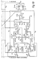
- A proximity-detection method for detection of passing magnetic articles comprising:a) sensing the ambient magnetic field, generating a voltage, VH, having an amplitude that is directly related to the magnetic field, and applying VH to the input of an amplifier to produce at an output thereof an amplified voltage, Vsig;b) providing a signal detector to which Vsig is applied, which detector produces a binary proximity-detector output voltage Vout having transitions of one polarity each time excursions of one polarity in Vsig reach a predetermined point therein;c) providing sources of DC off-set-limit voltages VA and VB that are respectively more positive and more negative than the center of the dynamic voltage range of said detector; andd) when at the output of said amplifier the median voltage, Vos, of Vsig is greater than VA, moving the entire signal Vsig in a negative direction, and when the median value, Vos, of Vsig is less than VB moving the entire signal Vsig in a positive direction to keep Vos within the range from VB to VA.
- The proximity-detection method of claim 1 additionally comprising the steps of:a) continuously generating one reference voltage VP2 that is equal to the most recent peak positive going excursion in Vsig;b) continuously generating another reference voltage VN2 that is equal to the most recent peak negative going excursion in Vsig; andc) generating the median voltage, Vos, that is about at the center of the voltage range between VP2 and VN2.
- The proximity-detection method of claim 1 wherein the steps of moving the entire signal Vsig is accomplished bycounting the transitions of at least one polarity in Vout during intervals when Vos is greater than VA and generating a digital signal for adding to Vsig a negative compensating off-set bias voltage by one predetermined negative bias increment at each transition of the one polarity in Vout, andcounting the transitions of at least one polarity in Vout during intervals when Vos is less than VB and generating a digital signal for adding to Vsig a positive compensating off-set bias voltage by one predetermined positive bias increment at each transition of the one polarity in Vout.
- The proximity-detection method of claim 1, wherein said amplifier is a digitally gain-controlled amplifier, the method additionally comprising:a) comparing the amplitudes of the excursions of at least one polarity in Vsig to a predetermined target value, VTG;b) generating a binary signal Vbig that changes from one to another binary level each time that Vsig exceeds the target value;c) applying the binary signal Vbig to the digitally-gain-controlled amplifier and when Vbig changes from the one to another binary level changing the gain of the digitally-gain-controlled amplifier by one predetermined gain increment in the direction to bring the peak values in Vsig to just below the predetermined target value.
- The proximity-detection method of claim 1 wherein said signal detector is of the peak-referenced-threshold signal-detector type, so that the transitions of one polarity in Vout from said signal detector occur at said point in Vsig after each peak excursion of one polarity at which the difference between the peak value and Vsig at said point equals a predetermined threshold value.
- The proximity-detection method of claim 1 wherein at any given time the median value, Vos, of Vsig at the output of said amplifier is the most recent voltage level centered between the positive and negative peaks of Vsig.
- The proximity-detection method of claim 1 wherein said signal detector is a peak-referenced-threshold detector that holds the peaks of at least one polarity until the signal retreats from each peak by a predetermined threshold voltage value that defines said predetermined point in Vsig.
Applications Claiming Priority (4)
| Application Number | Priority Date | Filing Date | Title |
|---|---|---|---|
| US852856 | 1992-03-17 | ||
| US84768397A | 1997-04-28 | 1997-04-28 | |
| US847683 | 1997-04-28 | ||
| US08/852,856 US6232768B1 (en) | 1996-01-17 | 1997-05-07 | Centering a signal within the dynamic range of a peak detecting proximity detector |
Publications (3)
| Publication Number | Publication Date |
|---|---|
| EP0875732A2 true EP0875732A2 (en) | 1998-11-04 |
| EP0875732A3 EP0875732A3 (en) | 2000-07-19 |
| EP0875732B1 EP0875732B1 (en) | 2004-03-03 |
Family
ID=27126727
Family Applications (1)
| Application Number | Title | Priority Date | Filing Date |
|---|---|---|---|
| EP98302576A Expired - Lifetime EP0875732B1 (en) | 1997-04-28 | 1998-04-01 | Method for centering a signal within the dynamic range of a peak detecting proximity detector |
Country Status (2)
| Country | Link |
|---|---|
| EP (1) | EP0875732B1 (en) |
| DE (1) | DE69822029T2 (en) |
Cited By (2)
| Publication number | Priority date | Publication date | Assignee | Title |
|---|---|---|---|---|
| GB2334636A (en) * | 1998-02-20 | 1999-08-25 | Lucas Ind Plc | Dynamic range control for a threshold detector |
| CN100565208C (en) * | 2007-08-13 | 2009-12-02 | 凌通科技股份有限公司 | The measuring method of the speed of conductor sliding on capacitance-type sensor |
Citations (2)
| Publication number | Priority date | Publication date | Assignee | Title |
|---|---|---|---|---|
| US4318617A (en) * | 1979-12-14 | 1982-03-09 | Keuffel & Esser Company | DC Shift error correction for electro-optical measuring system |
| DE19600803A1 (en) * | 1995-01-12 | 1996-07-18 | Nippon Denso Co | Magnetoresistive sensor signal processor using operational amplifiers |
-
1998
- 1998-04-01 EP EP98302576A patent/EP0875732B1/en not_active Expired - Lifetime
- 1998-04-01 DE DE69822029T patent/DE69822029T2/en not_active Expired - Lifetime
Patent Citations (2)
| Publication number | Priority date | Publication date | Assignee | Title |
|---|---|---|---|---|
| US4318617A (en) * | 1979-12-14 | 1982-03-09 | Keuffel & Esser Company | DC Shift error correction for electro-optical measuring system |
| DE19600803A1 (en) * | 1995-01-12 | 1996-07-18 | Nippon Denso Co | Magnetoresistive sensor signal processor using operational amplifiers |
Cited By (2)
| Publication number | Priority date | Publication date | Assignee | Title |
|---|---|---|---|---|
| GB2334636A (en) * | 1998-02-20 | 1999-08-25 | Lucas Ind Plc | Dynamic range control for a threshold detector |
| CN100565208C (en) * | 2007-08-13 | 2009-12-02 | 凌通科技股份有限公司 | The measuring method of the speed of conductor sliding on capacitance-type sensor |
Also Published As
| Publication number | Publication date |
|---|---|
| DE69822029T2 (en) | 2004-08-12 |
| EP0875732B1 (en) | 2004-03-03 |
| DE69822029D1 (en) | 2004-04-08 |
| EP0875732A3 (en) | 2000-07-19 |
Similar Documents
| Publication | Publication Date | Title |
|---|---|---|
| US6232768B1 (en) | Centering a signal within the dynamic range of a peak detecting proximity detector | |
| US5694038A (en) | Detector of passing magnetic articles with automatic gain control | |
| US6091239A (en) | Detection of passing magnetic articles with a peak referenced threshold detector | |
| US5650719A (en) | Detection of passing magnetic articles while periodically adapting detection thresholds to changing amplitudes of the magnetic field | |
| US6525531B2 (en) | Detection of passing magnetic articles while adapting the detection threshold | |
| EP0875733B1 (en) | Detection of passing magnetic articles using a peak-on-peak percentage threshold detector | |
| US6242908B1 (en) | Detection of passing magnetic articles while adapting the detection threshold | |
| EP0875774B1 (en) | Detection of passing magnetic articles while periodically adapting detection threshold | |
| US6100680A (en) | Detecting the passing of magnetic articles using a transducer-signal detector having a switchable dual-mode threshold | |
| EP2008064B1 (en) | Methods and apparatus for dynamic offset adjustment in a magnetic article detector | |
| US5729130A (en) | Tracking and holding in a DAC the peaks in the field-proportional voltage in a slope activated magnetic field sensor | |
| EP2391903B1 (en) | Magnetic field detector having a variable threshold | |
| EP0024836B1 (en) | Signal condition detector circuit | |
| US7619406B2 (en) | Methods and apparatus for magnetic article detection | |
| JP2007518989A (en) | Peak value detection circuit | |
| US8737012B2 (en) | System and method for automatic calibration of notch filter of hard disk drive | |
| EP0875732B1 (en) | Method for centering a signal within the dynamic range of a peak detecting proximity detector | |
| US5777465A (en) | Circuitry and method for sensing spatial transitions sensed with a magnetic sensor | |
| JP3005521B2 (en) | Proximity detection method for centering a signal within the dynamic range of a peak detection proximity detector | |
| GB1570568A (en) | Circuit and method for servo speed control | |
| JP3326933B2 (en) | Sensor signal processing device | |
| US4794579A (en) | Circuit for remote-scanning audio or video disk player for contactless scanning with coarse and fine drive mechanisms for radial servo readjustment | |
| US5864219A (en) | Circuit for detecting a level or a variation of an input direct voltage | |
| US20050040890A1 (en) | Automatic gain control device | |
| JPH0427040Y2 (en) |
Legal Events
| Date | Code | Title | Description |
|---|---|---|---|
| PUAI | Public reference made under article 153(3) epc to a published international application that has entered the european phase |
Free format text: ORIGINAL CODE: 0009012 |
|
| AK | Designated contracting states |
Kind code of ref document: A2 Designated state(s): BE DE FR GB IT |
|
| AX | Request for extension of the european patent |
Free format text: AL;LT;LV;MK;RO;SI |
|
| PUAL | Search report despatched |
Free format text: ORIGINAL CODE: 0009013 |
|
| AK | Designated contracting states |
Kind code of ref document: A3 Designated state(s): AT BE CH CY DE DK ES FI FR GB GR IE IT LI LU MC NL PT SE |
|
| AX | Request for extension of the european patent |
Free format text: AL;LT;LV;MK;RO;SI |
|
| RIC1 | Information provided on ipc code assigned before grant |
Free format text: 7G 01D 3/02 A, 7G 01D 5/244 B |
|
| 17P | Request for examination filed |
Effective date: 20000807 |
|
| AKX | Designation fees paid |
Free format text: BE DE FR GB IT |
|
| 17Q | First examination report despatched |
Effective date: 20020531 |
|
| GRAH | Despatch of communication of intention to grant a patent |
Free format text: ORIGINAL CODE: EPIDOS IGRA |
|
| GRAS | Grant fee paid |
Free format text: ORIGINAL CODE: EPIDOSNIGR3 |
|
| GRAA | (expected) grant |
Free format text: ORIGINAL CODE: 0009210 |
|
| AK | Designated contracting states |
Kind code of ref document: B1 Designated state(s): BE DE FR GB IT |
|
| REG | Reference to a national code |
Ref country code: GB Ref legal event code: FG4D |
|
| REF | Corresponds to: |
Ref document number: 69822029 Country of ref document: DE Date of ref document: 20040408 Kind code of ref document: P |
|
| ET | Fr: translation filed | ||
| PLBE | No opposition filed within time limit |
Free format text: ORIGINAL CODE: 0009261 |
|
| STAA | Information on the status of an ep patent application or granted ep patent |
Free format text: STATUS: NO OPPOSITION FILED WITHIN TIME LIMIT |
|
| 26N | No opposition filed |
Effective date: 20041206 |
|
| PGFP | Annual fee paid to national office [announced via postgrant information from national office to epo] |
Ref country code: IT Payment date: 20090421 Year of fee payment: 12 |
|
| PGFP | Annual fee paid to national office [announced via postgrant information from national office to epo] |
Ref country code: GB Payment date: 20090401 Year of fee payment: 12 |
|
| GBPC | Gb: european patent ceased through non-payment of renewal fee |
Effective date: 20100401 |
|
| PG25 | Lapsed in a contracting state [announced via postgrant information from national office to epo] |
Ref country code: GB Free format text: LAPSE BECAUSE OF NON-PAYMENT OF DUE FEES Effective date: 20100401 Ref country code: IT Free format text: LAPSE BECAUSE OF NON-PAYMENT OF DUE FEES Effective date: 20100401 |
|
| REG | Reference to a national code |
Ref country code: DE Ref legal event code: R082 Ref document number: 69822029 Country of ref document: DE Representative=s name: GRUENECKER, KINKELDEY, STOCKMAIR & SCHWANHAEUS, DE |
|
| REG | Reference to a national code |
Ref country code: DE Ref legal event code: R082 Ref document number: 69822029 Country of ref document: DE Representative=s name: GRUENECKER PATENT- UND RECHTSANWAELTE PARTG MB, DE Effective date: 20130617 Ref country code: DE Ref legal event code: R082 Ref document number: 69822029 Country of ref document: DE Representative=s name: GRUENECKER PATENT- UND RECHTSANWAELTE PARTG MB, DE Effective date: 20130708 Ref country code: DE Ref legal event code: R082 Ref document number: 69822029 Country of ref document: DE Representative=s name: GRUENECKER, KINKELDEY, STOCKMAIR & SCHWANHAEUS, DE Effective date: 20130708 Ref country code: DE Ref legal event code: R082 Ref document number: 69822029 Country of ref document: DE Representative=s name: GRUENECKER, KINKELDEY, STOCKMAIR & SCHWANHAEUS, DE Effective date: 20130617 Ref country code: DE Ref legal event code: R081 Ref document number: 69822029 Country of ref document: DE Owner name: ALLEGRO MICROSYSTEMS, LLC, WORCESTER, US Free format text: FORMER OWNER: ALLEGRO MICROSYSTEMS, LLC., WORCESTER, MASS., US Effective date: 20130708 Ref country code: DE Ref legal event code: R081 Ref document number: 69822029 Country of ref document: DE Owner name: ALLEGRO MICROSYSTEMS, LLC, WORCESTER, US Free format text: FORMER OWNER: ALLEGRO MICROSYSTEMS, INC., WORCESTER, MASS., US Effective date: 20130617 Ref country code: DE Ref legal event code: R081 Ref document number: 69822029 Country of ref document: DE Owner name: ALLEGRO MICROSYSTEMS, LLC, US Free format text: FORMER OWNER: ALLEGRO MICROSYSTEMS, INC., WORCESTER, US Effective date: 20130617 Ref country code: DE Ref legal event code: R081 Ref document number: 69822029 Country of ref document: DE Owner name: ALLEGRO MICROSYSTEMS, LLC, US Free format text: FORMER OWNER: ALLEGRO MICROSYSTEMS, LLC., WORCESTER, US Effective date: 20130708 |
|
| REG | Reference to a national code |
Ref country code: FR Ref legal event code: CJ Effective date: 20130821 Ref country code: FR Ref legal event code: CD Owner name: ALLEGRO MICROSYSTEMS, LLC, US Effective date: 20130821 |
|
| REG | Reference to a national code |
Ref country code: FR Ref legal event code: PLFP Year of fee payment: 18 |
|
| REG | Reference to a national code |
Ref country code: FR Ref legal event code: PLFP Year of fee payment: 19 |
|
| REG | Reference to a national code |
Ref country code: FR Ref legal event code: PLFP Year of fee payment: 20 |
|
| PGFP | Annual fee paid to national office [announced via postgrant information from national office to epo] |
Ref country code: FR Payment date: 20170327 Year of fee payment: 20 |
|
| PGFP | Annual fee paid to national office [announced via postgrant information from national office to epo] |
Ref country code: BE Payment date: 20170324 Year of fee payment: 20 |
|
| PGFP | Annual fee paid to national office [announced via postgrant information from national office to epo] |
Ref country code: DE Payment date: 20170329 Year of fee payment: 20 |
|
| REG | Reference to a national code |
Ref country code: DE Ref legal event code: R071 Ref document number: 69822029 Country of ref document: DE |
|
| REG | Reference to a national code |
Ref country code: BE Ref legal event code: MK Effective date: 20180401 |