EP0874405A2 - GaN group crystal base member having low dislocation density, use thereof and manufacturing methods thereof - Google Patents
GaN group crystal base member having low dislocation density, use thereof and manufacturing methods thereof Download PDFInfo
- Publication number
- EP0874405A2 EP0874405A2 EP98105090A EP98105090A EP0874405A2 EP 0874405 A2 EP0874405 A2 EP 0874405A2 EP 98105090 A EP98105090 A EP 98105090A EP 98105090 A EP98105090 A EP 98105090A EP 0874405 A2 EP0874405 A2 EP 0874405A2
- Authority
- EP
- European Patent Office
- Prior art keywords
- gan group
- gan
- crystal
- masked region
- mask layer
- Prior art date
- Legal status (The legal status is an assumption and is not a legal conclusion. Google has not performed a legal analysis and makes no representation as to the accuracy of the status listed.)
- Withdrawn
Links
Images


Classifications
-
- H—ELECTRICITY
- H01—ELECTRIC ELEMENTS
- H01L—SEMICONDUCTOR DEVICES NOT COVERED BY CLASS H10
- H01L33/00—Semiconductor devices with at least one potential-jump barrier or surface barrier specially adapted for light emission; Processes or apparatus specially adapted for the manufacture or treatment thereof or of parts thereof; Details thereof
- H01L33/02—Semiconductor devices with at least one potential-jump barrier or surface barrier specially adapted for light emission; Processes or apparatus specially adapted for the manufacture or treatment thereof or of parts thereof; Details thereof characterised by the semiconductor bodies
- H01L33/26—Materials of the light emitting region
- H01L33/30—Materials of the light emitting region containing only elements of group III and group V of the periodic system
- H01L33/32—Materials of the light emitting region containing only elements of group III and group V of the periodic system containing nitrogen
-
- H—ELECTRICITY
- H01—ELECTRIC ELEMENTS
- H01L—SEMICONDUCTOR DEVICES NOT COVERED BY CLASS H10
- H01L21/00—Processes or apparatus adapted for the manufacture or treatment of semiconductor or solid state devices or of parts thereof
- H01L21/02—Manufacture or treatment of semiconductor devices or of parts thereof
- H01L21/02104—Forming layers
- H01L21/02365—Forming inorganic semiconducting materials on a substrate
- H01L21/02367—Substrates
- H01L21/0237—Materials
- H01L21/02387—Group 13/15 materials
- H01L21/02389—Nitrides
-
- H—ELECTRICITY
- H01—ELECTRIC ELEMENTS
- H01L—SEMICONDUCTOR DEVICES NOT COVERED BY CLASS H10
- H01L21/00—Processes or apparatus adapted for the manufacture or treatment of semiconductor or solid state devices or of parts thereof
- H01L21/02—Manufacture or treatment of semiconductor devices or of parts thereof
- H01L21/02104—Forming layers
- H01L21/02365—Forming inorganic semiconducting materials on a substrate
- H01L21/02367—Substrates
- H01L21/0237—Materials
- H01L21/0242—Crystalline insulating materials
-
- H—ELECTRICITY
- H01—ELECTRIC ELEMENTS
- H01L—SEMICONDUCTOR DEVICES NOT COVERED BY CLASS H10
- H01L21/00—Processes or apparatus adapted for the manufacture or treatment of semiconductor or solid state devices or of parts thereof
- H01L21/02—Manufacture or treatment of semiconductor devices or of parts thereof
- H01L21/02104—Forming layers
- H01L21/02365—Forming inorganic semiconducting materials on a substrate
- H01L21/02436—Intermediate layers between substrates and deposited layers
- H01L21/02439—Materials
- H01L21/02455—Group 13/15 materials
- H01L21/02458—Nitrides
-
- H—ELECTRICITY
- H01—ELECTRIC ELEMENTS
- H01L—SEMICONDUCTOR DEVICES NOT COVERED BY CLASS H10
- H01L21/00—Processes or apparatus adapted for the manufacture or treatment of semiconductor or solid state devices or of parts thereof
- H01L21/02—Manufacture or treatment of semiconductor devices or of parts thereof
- H01L21/02104—Forming layers
- H01L21/02365—Forming inorganic semiconducting materials on a substrate
- H01L21/02436—Intermediate layers between substrates and deposited layers
- H01L21/02439—Materials
- H01L21/02483—Oxide semiconducting materials not being Group 12/16 materials, e.g. ternary compounds
-
- H—ELECTRICITY
- H01—ELECTRIC ELEMENTS
- H01L—SEMICONDUCTOR DEVICES NOT COVERED BY CLASS H10
- H01L21/00—Processes or apparatus adapted for the manufacture or treatment of semiconductor or solid state devices or of parts thereof
- H01L21/02—Manufacture or treatment of semiconductor devices or of parts thereof
- H01L21/02104—Forming layers
- H01L21/02365—Forming inorganic semiconducting materials on a substrate
- H01L21/02518—Deposited layers
- H01L21/02521—Materials
- H01L21/02538—Group 13/15 materials
- H01L21/0254—Nitrides
-
- H—ELECTRICITY
- H01—ELECTRIC ELEMENTS
- H01L—SEMICONDUCTOR DEVICES NOT COVERED BY CLASS H10
- H01L21/00—Processes or apparatus adapted for the manufacture or treatment of semiconductor or solid state devices or of parts thereof
- H01L21/02—Manufacture or treatment of semiconductor devices or of parts thereof
- H01L21/02104—Forming layers
- H01L21/02365—Forming inorganic semiconducting materials on a substrate
- H01L21/02612—Formation types
- H01L21/02617—Deposition types
- H01L21/0262—Reduction or decomposition of gaseous compounds, e.g. CVD
-
- H—ELECTRICITY
- H01—ELECTRIC ELEMENTS
- H01L—SEMICONDUCTOR DEVICES NOT COVERED BY CLASS H10
- H01L21/00—Processes or apparatus adapted for the manufacture or treatment of semiconductor or solid state devices or of parts thereof
- H01L21/02—Manufacture or treatment of semiconductor devices or of parts thereof
- H01L21/02104—Forming layers
- H01L21/02365—Forming inorganic semiconducting materials on a substrate
- H01L21/02612—Formation types
- H01L21/02617—Deposition types
- H01L21/02636—Selective deposition, e.g. simultaneous growth of mono- and non-monocrystalline semiconductor materials
- H01L21/02647—Lateral overgrowth
-
- H—ELECTRICITY
- H01—ELECTRIC ELEMENTS
- H01L—SEMICONDUCTOR DEVICES NOT COVERED BY CLASS H10
- H01L33/00—Semiconductor devices with at least one potential-jump barrier or surface barrier specially adapted for light emission; Processes or apparatus specially adapted for the manufacture or treatment thereof or of parts thereof; Details thereof
- H01L33/005—Processes
- H01L33/0062—Processes for devices with an active region comprising only III-V compounds
- H01L33/0066—Processes for devices with an active region comprising only III-V compounds with a substrate not being a III-V compound
- H01L33/007—Processes for devices with an active region comprising only III-V compounds with a substrate not being a III-V compound comprising nitride compounds
-
- H—ELECTRICITY
- H01—ELECTRIC ELEMENTS
- H01L—SEMICONDUCTOR DEVICES NOT COVERED BY CLASS H10
- H01L33/00—Semiconductor devices with at least one potential-jump barrier or surface barrier specially adapted for light emission; Processes or apparatus specially adapted for the manufacture or treatment thereof or of parts thereof; Details thereof
- H01L33/02—Semiconductor devices with at least one potential-jump barrier or surface barrier specially adapted for light emission; Processes or apparatus specially adapted for the manufacture or treatment thereof or of parts thereof; Details thereof characterised by the semiconductor bodies
- H01L33/025—Physical imperfections, e.g. particular concentration or distribution of impurities
-
- H—ELECTRICITY
- H01—ELECTRIC ELEMENTS
- H01S—DEVICES USING THE PROCESS OF LIGHT AMPLIFICATION BY STIMULATED EMISSION OF RADIATION [LASER] TO AMPLIFY OR GENERATE LIGHT; DEVICES USING STIMULATED EMISSION OF ELECTROMAGNETIC RADIATION IN WAVE RANGES OTHER THAN OPTICAL
- H01S2301/00—Functional characteristics
- H01S2301/17—Semiconductor lasers comprising special layers
- H01S2301/173—The laser chip comprising special buffer layers, e.g. dislocation prevention or reduction
-
- H—ELECTRICITY
- H01—ELECTRIC ELEMENTS
- H01S—DEVICES USING THE PROCESS OF LIGHT AMPLIFICATION BY STIMULATED EMISSION OF RADIATION [LASER] TO AMPLIFY OR GENERATE LIGHT; DEVICES USING STIMULATED EMISSION OF ELECTROMAGNETIC RADIATION IN WAVE RANGES OTHER THAN OPTICAL
- H01S2304/00—Special growth methods for semiconductor lasers
- H01S2304/12—Pendeo epitaxial lateral overgrowth [ELOG], e.g. for growing GaN based blue laser diodes
-
- H—ELECTRICITY
- H01—ELECTRIC ELEMENTS
- H01S—DEVICES USING THE PROCESS OF LIGHT AMPLIFICATION BY STIMULATED EMISSION OF RADIATION [LASER] TO AMPLIFY OR GENERATE LIGHT; DEVICES USING STIMULATED EMISSION OF ELECTROMAGNETIC RADIATION IN WAVE RANGES OTHER THAN OPTICAL
- H01S5/00—Semiconductor lasers
- H01S5/02—Structural details or components not essential to laser action
- H01S5/0206—Substrates, e.g. growth, shape, material, removal or bonding
- H01S5/0213—Sapphire, quartz or diamond based substrates
-
- H—ELECTRICITY
- H01—ELECTRIC ELEMENTS
- H01S—DEVICES USING THE PROCESS OF LIGHT AMPLIFICATION BY STIMULATED EMISSION OF RADIATION [LASER] TO AMPLIFY OR GENERATE LIGHT; DEVICES USING STIMULATED EMISSION OF ELECTROMAGNETIC RADIATION IN WAVE RANGES OTHER THAN OPTICAL
- H01S5/00—Semiconductor lasers
- H01S5/20—Structure or shape of the semiconductor body to guide the optical wave ; Confining structures perpendicular to the optical axis, e.g. index or gain guiding, stripe geometry, broad area lasers, gain tailoring, transverse or lateral reflectors, special cladding structures, MQW barrier reflection layers
- H01S5/22—Structure or shape of the semiconductor body to guide the optical wave ; Confining structures perpendicular to the optical axis, e.g. index or gain guiding, stripe geometry, broad area lasers, gain tailoring, transverse or lateral reflectors, special cladding structures, MQW barrier reflection layers having a ridge or stripe structure
-
- H—ELECTRICITY
- H01—ELECTRIC ELEMENTS
- H01S—DEVICES USING THE PROCESS OF LIGHT AMPLIFICATION BY STIMULATED EMISSION OF RADIATION [LASER] TO AMPLIFY OR GENERATE LIGHT; DEVICES USING STIMULATED EMISSION OF ELECTROMAGNETIC RADIATION IN WAVE RANGES OTHER THAN OPTICAL
- H01S5/00—Semiconductor lasers
- H01S5/30—Structure or shape of the active region; Materials used for the active region
- H01S5/32—Structure or shape of the active region; Materials used for the active region comprising PN junctions, e.g. hetero- or double- heterostructures
- H01S5/323—Structure or shape of the active region; Materials used for the active region comprising PN junctions, e.g. hetero- or double- heterostructures in AIIIBV compounds, e.g. AlGaAs-laser, InP-based laser
- H01S5/32308—Structure or shape of the active region; Materials used for the active region comprising PN junctions, e.g. hetero- or double- heterostructures in AIIIBV compounds, e.g. AlGaAs-laser, InP-based laser emitting light at a wavelength less than 900 nm
- H01S5/32341—Structure or shape of the active region; Materials used for the active region comprising PN junctions, e.g. hetero- or double- heterostructures in AIIIBV compounds, e.g. AlGaAs-laser, InP-based laser emitting light at a wavelength less than 900 nm blue laser based on GaN or GaP
Definitions
- the present invention relates to a GaN (gallium nitride) group crystal base member, use thereof (e.g., semiconductor light emitting element), and manufacturing methods thereof.
- GaN gallium nitride
- a conventional method for crystal growth of a GaN semiconductor material to give a thick film generally comprises forming a buffer layer of ZnO and the like on a sapphire substrate and growing a GaN semiconductor material by an HVPE method.
- An improved technique thereof involves the use of a substrate such as one made from spinel, LGO, LAO, ZnO, SiC and the like or a substrate showing easy cleavage performance, instead of the sapphire substrate.
- dislocation is meant here a defect that occurs when a semiconductor layer is grown on a substrate under a lattice mismatch. The dislocation thus created advances upward along with the growth of the crystal layer and passes through an active layer to form a continuous defective portion called a dislocation line (continuous dislocation).
- this dislocation acts as a non-radiative recombination center or as a path of a current to ultimately induce current leakage when such GaN semiconductor material is used for a light emitting element, which in turn degrades light emitting performance and shortens the service life.
- Another object of the present invention is to provide use of the aforementioned GaN group crystal base member.
- Yet another object of the present invention is to provide a method for producing the aforementioned GaN group crystal base member and a method for producing a light emitting element which is one use thereof.
- the GaN group crystal base member of the present invention comprises a base substrate, a mask layer partially covering the surface of said base substrate, and a GaN group crystal layer which is grown thereon to cover the above-mentioned mask layer and which is partially in direct contact with the non-masked region of the base substrate.
- Said base substrate allows growth of a GaN group crystal in the C axis orientation as the thickness direction, and the mask layer is made from a material substantially free from GaN group crystal growth.
- the base substrate partially covered with a mask layer is hereinafter simply called a "substrate for growth" to mean a substrate used to grow a GaN group crystal.
- the GaN group crystal layer grows from the non-masked region of the substrate for growth as the starting point until it covers the mask layer, whereby a GaN group crystal base member comprising the base substrate, mask layer and GaN group crystal layer is provided.
- the method for manufacturing the GaN group crystal base member of the present invention comprises partially covering the surface of the base substrate with a mask layer made from a material substantially free from crystal growth, and then growing a GaN group crystal layer from the non-masked region on the base substrate surface as the starting point to a thickness sufficient to cover said mask layer.
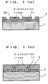
- Fig. 1(a), (b) are sectional views of the GaN group crystal base member of the present invention and its state during the ongoing growth.
- Fig. 2 shows one embodiment of the mask layer pattern used in the present invention.
- Fig. 3 is a sectional view of a conventional GaN group crystal base member.
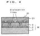
- Fig. 4 is a sectional view of another embodiment of the GaN group crystal base member of the present invention.
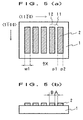
- Fig. 5 (a), (b) show one embodiment of the substrate for growth to be used in the present invention.
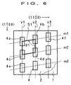
- Fig. 6 shows one embodiment of the substrate for growth to be used in the present invention and the arrangement pattern of the openings on the mask layer.
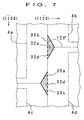
- Fig. 7 shows the effect of the arrangement pattern of the openings in the present invention.
- Fig. 8 (a), (b) show the growth of the crystal in the transverse direction from the openings in the present invention, wherein Fig. 8(a) shows the growth of a GaN group crystal in the transverse direction from one square opening (two-dot chain line) shown in Fig. 1 and Fig. 8(b) shows merger of GaN group crystals from four directions into one.
- Fig. 9 (a), (b) show the production steps of a GaN group light emitting diode using the substrate for growth of the present invention.
- Fig. 10 (a), (b) show examples of the width of the element and the width of the active part thereof.
- Fig. 11 is a perspective view showing the GaN group stripe lasers during production using the substrate for growth of the present invention, wherein the dotted lines on the both ends of the drawing are break lines and electrodes are omitted.
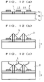
- Fig. 12 (a) - (c) show a method for controlling the dislocation line according to the present invention and one embodiment of the manufacturing method of the GaN group crystal base member of the present invention.
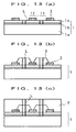
- Fig. 13 (a) - (c) show another method for controlling the dislocation line according to the present invention and another embodiment of the manufacturing method of the GaN group crystal base member of the present invention.
- Fig. 14 shows one embodiment of the GaN group light emitting element obtained by the method of Fig. 12.
- Fig. 15 shows one embodiment of the GaN group light emitting element obtained by the method of Fig. 13.
- Fig. 16 shows one embodiment of the structure of the GaN group crystal base member obtained by the manufacturing method of the present invention.
- the planes perpendicular to the above-mentioned ⁇ 1-100 ⁇ plane and parallel to the C axis are equivalently designated as ⁇ 11-20 ⁇ .
- the orientation perpendicular to the (1-100) plane is designated as [1-100] and the orientation collectively equivalent thereto is designated as ⁇ 1-100 ⁇ .
- the orientation perpendicular to the (11-20) plane is designated as [11-20] and the orientation collectively equivalent thereto is designated as ⁇ 11-20 ⁇ .
- the non-dislocation as referred to in the present invention means not only the ideal state completely free of dislocation which is theoretically possible, but also the state considered to have sufficiently low dislocation density to the degree the influence of the dislocation may be ignored from the industrial aspect, when compared to the dislocation density in the case where a GaN group crystal is grown on a sapphire substrate via a buffer layer.
- the material useful as a thick film layer includes those made from GaN, AlGaN, InGaN and the like.
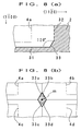
- the present inventors previously proposed forming mask layers 2 having a lattice pattern on a base substrate 1 to avoid cracks in the GaN layer caused by the different lattice constants as well as different coefficients of thermal expansion between GaN and sapphire substrate, and growing chip sized GaN layers 30 in the openings (non-masked region) exposing the substrate surface, as shown in Fig. 3 (Japanese Patent Unexamined Publication No. 273367/1995).
- the dislocation present in the above-mentioned crystals may continue from the base inclusive of the substrate or may be generated in certain growth interface and grow along with the crystal growth.
- the thickness necessary to cover the mask layer and the location of the low dislocation density part vary according to the direction of the mask layer (direction of the boundary line between the masked region and non-masked region) and atmospheric gas during GaN crystal growth.
- the mask layer 2 is completely embedded, and a bulky, thick GaN layer 3 which is flat and associated with no cracks and less defects can be obtained. It is speculated that the absence of cracks is attributable to the alleviation of the stress resulting from the fact that the mask layer 2 and GaN layer 3 are merely in contact with each other at the interface between them.
- the present invention is based on these findings.
- the surface of the base substrate 1 is partially covered by mask layer 2, and the GaN group crystal layer 3 grows from the non-masked region 11 of the base substrate 1 and covers the mask layer 2.
- the material of the above-mentioned base substrate 1 may be, for example, sapphire crystal (C face, A face), rock crystal, SiC and the like which are widely used to form GaN group crystal layers.
- sapphire substrate (C face) is preferred.
- the substrate may have a buffer layer of ZnO, MgO, AlN and the like on its surface to reduce the difference in the lattice constant and coefficient of thermal expansion between the substrate and GaN group crystal layer.
- Such base substrate can reduce the density of the dislocation newly generated from the non-masked region into a GaN group crystal layer 3 and afford a GaN group crystal layer 3 having fine crystallinity.
- the mask layer 2 should be one, from which surface a GaN group crystal does not substantially grow.
- examples of such material include non-crystalline materials such as nitrides and oxides of Si, Ti, Ta, Zr and the like, namely, SiO 2 , SiN x , SiO 1-x N x , TiO 2 , ZrO 2 and the like.
- SiO 2 , SiN x and SiO 1-x N x are suitable which are superior in heat resistance and which allow relatively easy film formation and removal by etching. These materials may be formed into a multilayer structure.
- the mask layer 2 may be formed by either an additive method or subtractive method.
- the subtractive method may comprise covering the entire substrate with a masking material by MOVPE, sputtering, CVD and the like and leaving a desired pattern by etching, thereby exposing the substrate surface to be used as a non-masked region.
- the mask layer 2 may have any pattern such as a lattice pattern, a stripe pattern and a dot pattern. Of these, a lattice pattern is preferable in that it enables efficient use of the surface area of the base substrate 1.
- the shape of one exposed part may be a quadrangle, a polygon or a circle.
- the rate of GaN group crystal growth in the transverse direction on the mask layer is greater in the growth in the ⁇ 11-20 ⁇ orientation than in the growth in the ⁇ 1-100 ⁇ orientation.
- this property be utilized to the maximum possible extent by setting the relation between the lattice width A in the ⁇ 11-20 ⁇ orientation and the lattice width B in the ⁇ 1-100 ⁇ orientation to 0 ⁇ A ⁇ B.
- the widths A, B of the lattice are preferably about 1 ⁇ m to 2 mm.
- the shape of the exposed part is quadrangle, it is an about 1 ⁇ m to 2 mm quadrangle.
- a GaN group crystal layer 3 is formed on the substrate for growth.
- the growth of the GaN group crystal starts from the non-masked region alone of the base substrate 1.
- the GaN group crystal layer 3 and the base substrate 1 directly contact with each other only at the non-masked region. Further growth completely buries the cavity as the non-masked region, and the top surface of the crystal becomes higher than the top surface of the mask layer 2.
- the GaN group crystal layer 3 can be grown by any method such as the HVPE method, the MOCVD method, the MBE method and the like.
- the HVPE method is preferable, but when a thin film is to be formed, the MOCVD method is preferable.
- a semiconductor light emitting element such as LED and LD (laser diode) can be produced by forming a light emitting part comprising a cladding layer and an active layer, and electrodes on the GaN group crystal base member of the present invention, particularly, a GaN group crystal layer 3 grown thick.
- the GaN group crystal base member (base substrate 1, first mask layer 2 and first GaN group crystal layer 3) shown in the above-mentioned Fig. 1 is used as a new base substrate M, on which a second mask layer 21 is formed in the same manner as in Fig. 1, thereby shutting off extension of the dislocation line, and then a second GaN group crystal layer 31 is grown thereon. In this manner, a GaN group crystal base member almost without dislocation can be obtained.
- the dislocation lines linearly rise from the non-masked region.
- the GaN group crystal base member obtained by forming the above-mentioned second GaN group crystal layer 31 is used as a new base substrate M, and a mask layer and a GaN group crystal layer may be repeatedly formed an optional number of times to form a GaN crystal having an almost non-dislocation state.
- a mask layer 2 is formed on the surface of a base substrate 1 to divide a masked region 12 from a non-masked region 11.
- the masked region 12 and non-masked region 11 are both linear strips which are alternately formed in a periodic repeat pattern.
- the longitudinal direction of the linear strips of the masked region and non-masked region extends in the ⁇ 1-100 ⁇ orientation.
- the preferable ranges are 1 ⁇ m ⁇ B ⁇ 20 mm and 1 ⁇ m ⁇ A+B ⁇ 25 mm, wherein the width of the masked region (namely, strip width in ⁇ 11-20 ⁇ orientation) is B and the width of the non-masked region is A (strip width in ⁇ 11-20 ⁇ orientation, as in B).
- the repeat pattern of the masked region and non-masked region may give stripes as shown in Fig. 5 or each strip may extend forming a certain angle with the ⁇ 1-100 ⁇ orientation. In either way, the masked region and non-masked region form a regular repeat pattern in the ⁇ 11-20 ⁇ orientation, as well.
- the repeat pattern of the masked region and non-masked region may form a zigzag line.
- a repeat pattern of strips forming an optional curves, such as sign curve, a repeat pattern concentrically forming an annulus ring or hexagon masked region, a coiled repeat pattern and the like may be employed.
- a repeat pattern in which the ratio of A to B varies according to a certain relational formula may be used.
- the width B of the masked region corresponds to the width of the low dislocation density GaN group crystal to be grown thereon.
- a width suitable for use may be determined within said width, wherein it may be used as it is or divided before use.
- B exceeds 20 mm, the GaN group crystal will require a long time to cover the masked region. Nevertheless, when B is less than 2 ⁇ m, a mask layer cannot be formed easily, and the ratio of B to A+B becomes smaller to result in less reduction of dislocation density of the GaN group crystal obtained.
- the non-masked region is preferably as small as possible, so that the limited area on the base substrate can be used most effectively and the largest possible area of the non-dislocation part is obtained at high speed. It is preferable that the proportional relation of A and B is always A ⁇ B. It is more preferable to set the proportion of B to A+B to 50% - 99.998%, particularly 50% - 99.98%. When the proportion of B to A+B exceeds 99.998%, A becomes too small to prevent easy formation of the non-masked region, and B becomes greater to require a large amount of time for the GaN group crystal to cover the masked region.
- an off-facet plane 32 grows in the ⁇ 11-20 ⁇ orientation at high speed and a facet plane 31 grows moderately in the ⁇ 1-100 ⁇ orientation from the side extending in the ⁇ 11-20 ⁇ orientation.
- the off-facet plane is shown with a thick dotted line and the facet plane is shown with a thick line.
- the transverse growth planes can be considered to be only two planes in the directions orthogonally crossing with each other (e.g., Fig. 8(a), 31 and 32). As the growth proceeds, however, a facet plane 33 appears at the corner where the planes 31 and 32 cross with each other.
- a continued crystal growth results in enclosure of the central portion (vicinity of center point m ) which is located at the same distance from the four openings 4a, 4b, 4c and 4d. It occurs at a certain point of the growth by the facet planes 33a, 33b, 33c and 33d slow in growth, as shown in Fig. 8(b).
- the enclosed area requires a long time to be closed by a continued crystal growth. During that long time period, the crystal continues to grow at high speed in the thickness direction (C axis orientation). By the time the enclosed area is filled, the thickness of the crystal becomes unnecessarily great far exceeding the intended size.
- the central part (center point m ) filled last consists of the crystals from the four directions which are joined at one point, having a low crystal quality with many defects.
- the pattern formed by the openings is set to be other than an orthogonal matrix formed by the openings in the ⁇ 11-20 ⁇ orientation and ⁇ 1-100 ⁇ orientation, but parallelogram (exclusive of square and rectangle) or square without the side in the ⁇ 11-20 ⁇ orientation.
- parallelogram exclusive of square and rectangle
- the enclosure only by the facet planes can be avoided and at least one of the above-mentioned problems-can be solved.
- the position of the openings may be moved so that the central portion will be enclosed by two facet planes and one off-facet plane, whereby the remaining problems mentioned above can be entirely solved.
- a mask layer 2 (partially broken away in the Figure) and on the mask layer 2 are formed plural openings 4 in which the top surface of the base substrate 1 is exposed at the bottom.
- the pattern formed by the openings 4 at the top surface of the mask layer 2 is drawn by supposing a net having a quadrangle S1 (shown in a thick line) as the minimum constituent unit, on the surface of the mask layer.
- the openings 4 are formed on the intersection of the net lines.
- this quadrangle S1 of the net may be a parallelogram or a square or rectangle without the side in the ⁇ 11-20 ⁇ orientation.
- quadrangle S1 of the net is a parallelogram S1 formed by a part of the parallel two straight lines y1 and y2 extending in the ⁇ 1-100 ⁇ orientation, as parallel two sides.
- the openings near the outer periphery may be increased or decreased in number by, for example, omitting openings 4e and 4f according to the outer shape of the substrate.
- the net pattern may be, as shown in the embodiment of Fig. 6, completely congruent parallelogram defined only by the parallel lines in two directions, a pattern wherein mirror symmetrical parallelograms are alternately combined, a pattern wherein different parallelograms are combined and the like.
- the shape of the parallelogram constituting the net pattern is preferably one wherein one of the two sides slides in the ⁇ 1-100 ⁇ orientation from the other side by half the length of said side.
- it is a parallelogram wherein, of the openings 4a, 4b, 4c and 4d at the four vertexes of the parallelogram, the sets (4a, 4c and 4d) and (4a, 4d and 4b) come to the vertex of each isosceles triangle.
- the distance between the openings in the ⁇ 1-100 ⁇ orientation is about 1 ⁇ m - 10 ⁇ m, whereas that in the ⁇ 11-20 ⁇ orientation along which the crystal grows at high speed is about 2 ⁇ m - 50 ⁇ m.
- inventions of the net pattern include one wherein the minimum constituent unit quadrangle of the net is a parallelogram having two parallel sides extending in the ⁇ 11-20 ⁇ orientation, or a parallelogram including no straight line extending in the ⁇ 1-100 ⁇ orientation or ⁇ 11-20 ⁇ orientation, and the like.
- the plane 32 in the ⁇ 1-100 ⁇ orientation of the crystal which grows from the opening decreases due to the growth of the off-facet plane 33.
- the shape of the opening is preferably one wherein the side in the ⁇ 1-100 ⁇ orientation has a sufficient length. To be specific, it is a quadrangle having a size falling within the range specified by 10 ⁇ m - 10 mm in the ⁇ 1-100 ⁇ orientation and 1 ⁇ m - 10 ⁇ m in the ⁇ 11-20 ⁇ orientation, and having a longer side in the ⁇ 1-100 ⁇ orientation.
- low dislocation density and high quality crystal formed on the masked region or non-masked region is utilized to form a GaN group semiconductor element using the low dislocation density part.
- the width of the masked region and non-masked region be not less than the width of the active part of the element and not more than the width of the entire element.
- the element is manufactured in such a manner that the masked region comes at least right beneath the active layer of the element. In this way, a high quality element can be ensured using the least possible part of the masked region.
- GaN group semiconductor layer is formed to give a laminate including a number of elements, and the part above the mask layer has a low dislocation density, each element is preferably divided at the non-masked region. This obliterates useless breaking of high quality crystal parts when dividing the elements.
- the element to be the production target is not particularly limited, the element may be, for example, a light emitting element, a light receiving element, power device and the like.
- the light emitting element exemplified are GaN group LED and GaN group semiconductor laser
- examples of power device include microwave FET, power MOSFET, HBT (heterojunction bipolar transistor), MMIC (monolithic microwave integrated circuit) and the like.
- Fig. 10(a) shows a GaN group LED having a GaN crystal as a substrate 1.
- the element as a whole is a simple rectangular parallelopiped wherein the width D of the element and the width E of the active part k1 are the same.
- Fig. 10(b) shows a GaN group LED having a sapphire crystal as a substrate, wherein the substrate is an insulating member requesting the electrode disposed at the upper side as shown in the Figure, and the width E of the active part k1 is smaller than the width D of the element.
- FIG. 10(c) shows a GaN group stripe laser having a sapphire crystal as a substrate, wherein the stripe structure necessitates the width E of the active part (stripe part) to be still smaller than the width D of the element, as compared to the LED of Fig. 10(b).
- the part to be the width of the stripe part varies according to the embodiment of the laser element.
- the width of the stripe part corresponds to the width of the member when the stripe member is embedded; the width of a laminate in an embodiment where the width of the laminate between two planes of resonators is narrowed to make the shape of the laminate itself a stripe; and the width of an electrode where the electrode is a stripe and the part of the active layer, which comes beneath the electrode, becomes a stripe part.
- the embodiment shown in Fig. 10(c) has a width E of the stripe part k1 which is smaller than the width of the entire active layer.
- the width of the element in Fig. 10 and the depth size of the element in the direction perpendicular to the paper surface vary depending on the kind of element, inclusive of one having a large area (e.g., LED array).
- the size of a light emitting element such as a laser is about width 200 ⁇ m - 500 ⁇ m and depth 200 ⁇ m - 1000 ⁇ m per one element.
- the width w1 between the two parallel straight lines p1 and p2 extending in the ⁇ 1-100 ⁇ orientation should be equal to the width of the production target element, particularly at least the width capable of being set beneath the active part. This enables efficient use of a high quality crystal above the masked region for an element, as shown in Fig. 9(b) and Fig. 11.
- a mask layer When the part above the masked region has a low dislocation density, it is preferable that a mask layer have two parallel straight lines extending in the ⁇ 1-100 ⁇ orientation which define the outer shape.
- the width between the two straight lines need only be that allowable to come beneath the active part, which may be selected from the range of from the width of the active part of the element to the width of the entire element.
- the width of the masked region In the case of a stripe laser, for example, since it has a width selected from the range of from the width of the stripe (2 ⁇ m ) to the width of the entire element (1000 ⁇ m), the width of the masked region should be also 2 ⁇ m - 1000 ⁇ m. In the case of an LED array having a greater area, at least the width of the masked region is set to fall within the range of from the width of the active part to the width of the entire element.
- the masked region forms a stripe as shown in Fig. 5 and elements are formed above the masked region strips, a number of elements may be formed sequentially and integrally in the longitudinal direction above one masked region strip, and divided at a final stage.
- the width of the non-masked region then may be any as long as the division is effected.
- the width of the masked region and that of the active part are the same, the width of the masked region becomes minimum and that of the non-masked region at both sides thereof becomes maximum.
- the non-masked region becomes the starting point of the GaN group crystal layer growth as well as the cutting region for division.
- the width need only be that necessary as the starting point of the crystal growth rather than the width necessary for division, since the division scarcely requires a loss width.
- the loss should be considered to be about 20 ⁇ m - 50 ⁇ m.
- the width of the non-masked region is selected from the range of from about 0.5 ⁇ m - 5 mm, particularly from about 1 ⁇ m - 1 mm, when a low dislocation density part is to be formed above the masked region.
- the method for manufacturing the element of the present invention as shown in Fig. 9(a), wherein the part above the masked region of the GaN group crystal layer has a low dislocation density comprises growing a semiconductor layers k in such a manner that the active part comes at least above the masked region and forming a laminate containing a necessary number of elements.
- the element is a simple GaN group LED wherein the width of the mask, that of the element and that of the active part are the same.
- the active part which assumes the function of an element produces emission of light and includes a pn junction.
- the laminate containing the necessary number of elements is divided to separate each element.
- the base substrate may or may not be removed.
- the element is a stripe laser, it is preferably formed and divided taking note of the fact that the stripe portion extends in the longitudinal direction and that the element contains a resonator.
- the longitudinal direction of the part to be a stripe part is the longitudinal direction of each masked region as shown in Fig. 11, and plural stripe lasers are efficiently formed in sequence above the masked region.
- the entire laminate is divided along the plane perpendicular to the longitudinal direction of the stripe part, before division into each stripe part (e.g., division along X1 and X2 in Fig. 11) to form a string of adjoining elements in the ⁇ 11-20 ⁇ orientation as shown in Fig. 11.
- each GaN group stripe laser is efficiently separated by cutting along the plane parallel to the longitudinal direction of the stripe part (e.g., in Fig. 11, division along U1 to U4).
- the dislocation line present in the GaN group crystal layer 3 has been considered to advance linearly in the thickness direction along with the growth of the layer, as shown in Fig. 1. Nevertheless, the present inventors have claimed that the dislocation line generated in the non-masked region can be freely led to the part above the masked region or non-masked region by determining a mask layer pattern, crystal growth method and atmospheric gas during the crystal growth in combination. In other words, in the GaN single crystal layer 3 in Fig. 1, any part above the masked region and non-masked region can be made to have a low dislocation density.
- a mask layer 2 is formed on the base substrate 1 (wherein 12 is a masked region and 11 is a non-masked region), and GaN group crystal is grown from the non-masked region.
- the ratio of the growth rate in the C axis orientation (thickness orientation) of said GaN group crystal and that in the orientation perpendicular to the C axis (transverse direction) is controlled to vary the crystal growth to the following (i) or (ii).
- the controlling factors of the ratio of the above-mentioned growth rate in the C axis orientation and that in the orientation perpendicular to the C axis are the pattern formed by the mask layer, crystal growth method and atmospheric gas during the crystal growth, and achievement of the above-mentioned crystal growth modes (i) and (ii) hinges on certain combination of these factors.
- the pattern of the mask layer is based on the direction of the boundary line between the masked region and non-masked region.
- the boundary line between the masked region and non-masked region is a straight line extending in the ⁇ 1-100 ⁇ orientation
- the off-facet plane grows in the transverse direction at a higher rate.
- the surface of the mask layer is covered while the GaN group crystal layer is still thin, as compared to the case of ⁇ 11-20 ⁇ orientation to be mentioned next.
- the boundary line between the masked region and non-masked region is a straight line extending in the ⁇ 11-20 ⁇ orientation
- the ⁇ 1-100 ⁇ plane which is a facet plane
- the ⁇ 1-100 ⁇ plane extends beyond this boundary line into the transverse direction, making the growth rate in the transverse direction slower.
- slant facet such as ⁇ 1-101 ⁇ plane tends to be formed. It necessitates making the plane flat after the pyramid plane is formed first. Consequently, the flat plane requires a certain thickness.
- One example of the pattern showing the most noticeable effect of the above-mentioned mask pattern is the stripe one shown in Fig. 5.
- the longitudinal direction of this strip is the direction of the boundary line between the above-mentioned masked region and non-masked region.
- crystal growth method examples include HVPE, MOCVD and the like.
- HVPE high vacuum chemical vapor deposition
- MOCVD metalorganic chemical vapor deposition
- the HVPE method affording a higher growth rate is preferred.
- the atmospheric gas is exemplified by H 2 , N 2 , Ar, He and the like, and H 2 and N 2 are preferably used for controlling the dislocation line.
- the growth rate in the C axis orientation becomes higher.
- the direction of the boundary line between the masked region and non-masked region is a straight line in the ⁇ 11-20 ⁇ orientation, namely, slow in the transverse direction
- the ratio of the rate in the C axis orientation becomes significantly greater, thereby making the crystal above the non-masked region have a low dislocation density.
- the growth rate in the C axis orientation becomes lower than that when an H 2 rich atmosphere is employed, as a result of which the growth rate in the transverse direction becomes relatively greater.
- the growth rate in the transverse direction is accelerated by the combination with the mask pattern, the crystal above the masked region comes to have a low dislocation density, as shown in Fig. 13.
- the crystal growth by MOCVD is mainly carried out under an H 2 rich atmosphere.
- H 2 rich atmosphere For example, when a combination of carrier gas hydrogen (10 L)+hydrogen gas (100 cc) for organic metal bubbling as a III group gas and carrier gas hydrogen (5 L) +ammonia (5 L) as a V group gas are used, a hydrogen concentration is 75%, which is one example of H 2 rich atmosphere having 0% nitrogen concentration.
- the nitrogen concentration when the III group carrier gas is changed to nitrogen is about 50%.
- the nitrogen concentration is about 25%.
- a gas having a nitrogen concentration of not less than about 25% is designated to be N 2 rich.
- the part of the GaN group crystal having a low dislocation density which is obtained by intentionally avoiding the passage of the dislocation line is positioned at the center of a light emitting part of a light emitting layer, so that a preferable light emitting element as shown in Figs. 14 and 15 can be obtained.
- the element shown in Fig. 14 is one embodiment of the GaN group LED of the present invention, wherein, in the active layer 5 of the element, the part above the non-masked region has a low dislocation density. This part having a low dislocation density is the center of the light emission due to a current stricture structure. In contrast, in the active layer 5 of the element of the GaN group LED shown in Fig. 15, the part above the masked region has a low dislocation density and is the center of the light emission.
- the GaN group crystal has greatly grown in the thickness direction as well when the GaN group crystal has completely covered the mask layer, which inevitably increases the thickness T from the top surface of the mask layer to the top surface of the GaN group crystal layer.
- the width W of the mask layer is reduced, however, the GaN group crystal quickly covers the mask layer completely, thereby making the thickness T smaller.
- the ratio of the thickness T from the top surface of the mask layer of the GaN group crystal layer to the width W of the mask layer, T/W cannot become smaller than a certain level. This in turn has resulted in the problem that a GaN group crystal layer formed on a sufficiently wide masked region inevitably becomes thick and is associated with cracks and warping.
- the present invention suggests, as stated with respect to the method for controlling the direction of the above-mentioned dislocation line, that the pattern of the mask layer be such having the boundary line between the masked region and non-masked region extending in the ⁇ 1-100 ⁇ orientation, the GaN group crystal be grown by MOCVD (Metal Organic Chemical Vapor Deposition) and the atmospheric gas in which the GaN group crystal is grown by the MOCVD be an N 2 rich gas.
- MOCVD Metal Organic Chemical Vapor Deposition
- the ratio of the thickness T of the GaN group crystal layer 3 covering the mask layer 2 formed on the base substrate 1 to the width W of the mask layer 2 in the ⁇ 11-20 ⁇ orientation, T/W, becomes not more than 1.75, whereby a thin GaN group crystal layer conventionally unattainable as shown in Fig. 16 can be obtained.
- a 20 nm thick AlN buffer layer was grown at a low temperature using a MOVPE device on a sapphire substrate (C face) having a diameter of 2 inches and a thickness of 330 ⁇ m, and a 1.5 ⁇ m GaN thin layer was grown thereon to give a base substrate.
- An SiO 2 thin film having a thickness of 500 nm was formed as a masking material on the surface of this substrate by a sputtering method, and a mask layer was formed by leaving the mask material in a lattice pattern at a line width of 100 ⁇ m and 200 ⁇ m pitch by etching. That is, 100 ⁇ m square exposed parts were arrayed at 200 ⁇ m intervals.
- This new substrate was set in an HVPE device to grow 300 ⁇ m thick n-type GaN layer. The mask layer was completely embedded, wherein the surface flatness was fine, and a 2 inch diameter n-type GaN group crystal base member was obtained.
- the GaN on the mask layer was evaluated by TEM. As a result, the dislocation density was not more than 1 ⁇ 10 2 cm - 2 .
- a 50 nm thick AlN buffer layer and a 1.5 ⁇ m GaN thin layer were grown on a sapphire substrate (C face) having a diameter of 2 inches and a thickness of 330 ⁇ m to give a base substrate.
- the mask pattern was a stripe wherein 500 nm thick, 200 ⁇ m wide linear SiO 2 mask layers and 200 ⁇ m wide exposed parts were alternately disposed.
- the longitudinal direction of the stripe was the ⁇ 1-100 ⁇ orientation. This was set in an HVPE device to grow a 220 ⁇ m thick n-type GaN layer.
- the mask layer was completely embedded without occurrence of cracks, whereby a 2 inch diameter n-type GaN group crystal base member having fine surface flatness was obtained.
- Example 2 In the same manner as in Example 1, a mask layer having a lattice pattern and an n-type GaN layer were grown on a base substrate. A second mask layer having the same lattice pattern as in Example 1 was grown on this n-type GaN layer. This second mask layer covered right above the non-masked region. This was set in an HVPE device to grow a 300 ⁇ m thick second n-type GaN layer.
- the second n-type GaN layer thus obtained was evaluated by TEM. As a result, the dislocation density was not more than 1 ⁇ 10 2 cm -2 .
- a mask layer made from an SiO 2 thin film was formed by a sputtering method so that a linear strip pattern as shown in Fig. 5 was drawn on the surface of the base substrate similar to that used in Example 1 to give a substrate for growth.
- the mask layer was formed to have strips extending in the ⁇ 1-100 ⁇ orientation.
- a GaN crystal was grown on this substrate for growth by an HVPE device at a 50 ⁇ m/hr growth rate for 4 hr to give a 200 ⁇ m thick GaN crystal layer.
- the dislocation density of the GaN crystal grown on the masked region was evaluated by TEM. As a result, the dislocation density was not more than 1 ⁇ 10 4 cm -2 .
- the sapphire substrate was removed by abrasion to give a flat GaN crystal substrate.
- a 25 ⁇ m thick GaN crystal was grown under the conditions wherein the width B of the masked region was 1 ⁇ m, the width A of the non-masked region was 1 ⁇ m and the proportion of B to A+B was 50%.
- a 11 mm thick GaN crystal was grown in the same manner as in Example 1 under the conditions wherein the width B of the masked region was 20 mm, the width A of the non-masked region was 0.5 ⁇ m and the proportion of B to A+B was 99.998%.
- the sapphire substrate was removed by abrasion to give a GaN single crystal substrate which was a thick, bulky and flat crystal having a wide area.
- the irregularities on the surface were somewhat greater than those found in Examples 1 to 3.
- the width of the masked region should be 20 mm at the greatest.
- the width of the masked region is greater than this, the time necessary for the step becomes longer and the surface morphology tends to be degraded.
- the width A of the non-masked region was 0.5 ⁇ m, it was found that the width A of less than 0.5 ⁇ m was difficult to achieve.
- the proportion of B to A+B is preferably about 99.998% at the greatest.
- a 11 mm thick GaN crystal was grown in the same manner a sin Example 1 under the conditions wherein the width B of the masked region was 20 mm, the width A of the non-masked region was 5 mm and the proportion of B to A+B was 80%.
- the GaN crystal layer contained numerous cracks extending from the non-masked region to the masked region.
- a greater width of the non-masked region was not desirable due to the occurrence of cracks, and the upper limit of A was 5 mm.
- An SiO 2 mask layer was formed on the surface of the base substrate similar to that used in Example 1. Then, openings were formed by etching to give a substrate for growth of the type shown in Fig. 6. The shape of the openings was congruent, which was a rectangle having the size of ⁇ 11-20 ⁇ orientation 3 ⁇ m ⁇ ⁇ 1-100 ⁇ orientation 100 ⁇ m.
- the pattern of the disposed openings was such that the width of the masked region sandwiched between the adjacent openings was 5 ⁇ m in the ⁇ 11-20 ⁇ orientation and 2 ⁇ m in the ⁇ 1-100 ⁇ orientation, and the shape of parallelogram of the net pattern was such that one of the two sides in the ⁇ 1-100 ⁇ orientation slid by a half of the length of the side in the ⁇ 1-100 ⁇ orientation.
- the above-mentioned substrate for growth was set on an HVPE device, and a 200 ⁇ m thick GaN group crystal layer was formed from the non-masked region as the starting point.
- the GaN group crystal grew on the mask layer in the transverse direction as well to completely cover the mask layer.
- the flatness of the GaN group crystal layer surface was fine.
- the part formed by the crystals that grew in the transverse direction and joined from each opening further grew in the thickness direction after the joining.
- the surface layer and the vicinity thereof had fine crystal quality.
- the objective element to be formed was a stripe laser.
- the mask layer was a parallel stripe extending in the ⁇ 1-100 ⁇ orientation of GaN crystal.
- the substrate for growth was prepared in the same manner as in Example 1, wherein the pattern of the mask layer was width 150 ⁇ m and the central pitch 300 ⁇ m.
- a 100 ⁇ m GaN crystal layer was formed on the substrate for growth to give a substrate, on which were sequentially grown in its entirety n-GaN layer/n-AlGaN layer/n-GaN layer/InGaN multi-quantum well layers/p-AlGaN layer/p-GaN layer/p-AlGaN layer/p-GaN layer.
- the laminate was etched by RIE (Reactive Ion Etching) leaving 8 ⁇ m width strips to give a stripe laminate as shown in Fig. 11 by k.
- the stripe was aligned with the about center of the mask layer, so that the stripe could be in the ⁇ 1-100 ⁇ orientation.
- Abrasion removed the sapphire substrate (C face) to make the entire thickness 80 ⁇ m.
- This Example confirmed efficient forming of elements by aligning the masked region with the stripe part.
- efficient production of stripe lasers was attained.
- the dislocation line was bent to the part above the masked region to make the part above the non-masked region a low dislocation density part.
- the most basic crystal substrate used was a sapphire substrate (C face). On the surface thereof, an AlN low temperature buffer layer and GaN layer were grown to the thickness of 2 ⁇ m to give a base substrate.
- the substrate was taken out from the growth apparatus and an SiO 2 mask layer was formed by sputtering.
- the pattern of the mask layer was a stripe wherein the longitudinal direction of the strip was the ⁇ 11-20 ⁇ orientation of the GaN group crystal to be grown.
- this specimen was placed in an MOCVD device and heated to 1000°C under a hydrogen atmosphere containing ammonia. TMG and ammonia were flown for 30 min to grow GaN crystal.
- the GaN crystal first grew in a pyramid shape as shown in Fig. 12(b), and the dislocation line was bent toward the masked region side. The crystal was further grown until it became flat at 10 ⁇ m.
- a current blocking layer 6 was formed in such a manner that the low dislocation density part came to the light emitting center of the light emitting layer 5 to form a light emitting element. As a result, one having a high light emission efficiency was prepared.
- 7 is an upper cladding layer and 8 and 9 are electrodes.
- Example 2 In the same manner as in Example 1 except that the mask layer stripe had a longitudinal direction which was the ⁇ 1-100 ⁇ orientation of the GaN group crystal to be grown and the atmospheric gas was nitrogen rich, a GaN group crystal layer was formed. The thickness until it became flat was 2 ⁇ m.
- a current blocking layer 6 was formed in such a manner that the low dislocation density part came to the light emitting center of the light emitting layer 5 to form a light emitting element. As a result, a light emitting element having a high light emission efficiency was obtained.
- 7 is an upper cladding layer and 8 and 9 are electrodes.
- the most basic crystal substrate used was a sapphire substrate (C face). On the surface thereof, an AlN low temperature buffer layer and GaN layer were grown to the thickness of 2 ⁇ m to give a base substrate.
- An SiO 2 mask layer was formed by sputtering.
- the pattern of the mask layer was a stripe wherein the longitudinal direction of the strip was the ⁇ 1-100 ⁇ orientation of the GaN group crystal to be grown.
- the width of the strip of the non-masked region was 4 ⁇ m and the width W of the strip of the masked region was 4 ⁇ m.
- this specimen was placed in an MOCVD device and heated to 1000°C under a nitrogen rich atmospheric gas (III group carrier gas nitrogen (10 L), gas (100 cc) for organic metal bubbling, V group carrier gas hydrogen (5 L), ammonia (5 L)).
- a nitrogen rich atmospheric gas III group carrier gas nitrogen (10 L), gas (100 cc) for organic metal bubbling, V group carrier gas hydrogen (5 L), ammonia (5 L)
- TMG and ammonia were fed to grow GaN crystal.
- the GaN crystal at the point the surface of the mask layer was completely embedded had a thickness T of 2 ⁇ m, as shown in Fig. 16. Thus, T/W was 0.5.
- Example 2 In the same manner as in Example 1 except that the atmospheric gas was changed from nitrogen rich to hydrogen rich, a GaN crystal was grown.
- the GaN crystal at the point the surface of the mask layer was completely embedded had a thickness T of 7 ⁇ m. Thus, T/W was 1.75.
- Example 2 In the same manner as in Example 1 except that the atmospheric gas was changed from nitrogen rich to hydrogen rich and the longitudinal direction of the stripe of the mask layer was the ⁇ 11-20 ⁇ orientation, a GaN crystal was grown. The GaN crystal at the point the surface of the mask layer was completely embedded had a thickness T of 12 ⁇ m. Thus, T/W was 3.
Abstract
Description
Claims (19)
- A GaN group crystal base member comprising a base substrate, a mask layer partially covering the surface of said base substrate to give a masked region, and a GaN group crystal layer grown thereon to cover said mask layer, which is partially in direct contact with a non-masked region of the base substrate.
- The GaN group crystal base member of claim 1, wherein the base substrate permits growth of a GaN group crystal in the C axis orientation as the thickness direction, and the mask layer is made from a material substantially free from GaN group crystal growth.
- The GaN group crystal base member of claim 1, wherein the base substrate has at least a surface layer represented by the formula: InxGayAlzN wherein 0≦X≦1, 0≦Y≦1, 0≦Z≦1, X+Y+Z=1.
- The GaN group crystal base member of claim 1, wherein the GaN group crystal layer is a first GaN group crystal layer, which further comprises a second mask layer partially covering the surface of said first GaN group crystal layer and a second GaN group crystal layer grown thereon to cover the second mask layer, which is partially in direct contact with a non-masked region of the first GaN group crystal layer.
- The GaN group crystal base member of claim 2, wherein a masked region and a non-masked region are alternately repeated periodically, said periodic repetition comprising at least a repetition in a 〈11-20〉 orientation of the GaN group crystal to be grown on said base substrate, a width B of said masked region in the 〈11-20〉 orientation and a width A of said non-masked region being defined by 1 µm≦B≦20 mm and 1 µm<A+B≦25 mm.
- The GaN group crystal base member of claim 2, wherein the mask layer has plural openings on the surface thereof, the base substrate being exposed at the bottom of the openings, an arrangement pattern of said openings on the surface of the mask layer being one wherein the openings are positioned at intersections of net lines forming a quadrangle as the smallest constituent unit, said quadrangle being a square without a side in the 〈11-20〉 orientation of the GaN group crystal to be grown on the base substrate, or parallelogram.
- The GaN group crystal base member of claim 2, wherein the ratio of a thickness T of the GaN group crystal layer covering the mask layer from the mask layer surface to a width W of the mask layer in the 〈11-20〉 orientation is T/W<1.75.
- The GaN group crystal base member of claim 2 to be used as a crystal substrate of a GaN group semiconductor element, wherein the GaN crystal layer has grown to cover the mask layer from a non-masked region as the growth starting point, and the mask layer forms a pattern wherein the width of the part having a low dislocation density within said crystal exceeds the width of an active part of said GaN group semiconductor element.
- The GaN group crystal base member of claim 2 to be used as a crystal substrate of a GaN group semiconductor element, wherein a masked region having, as outer shape lines, two parallel straight lines extending in the 〈1-100〉 orientation of the GaN group crystal to be grown on said base substrate, and the width between the two straight lines being not more than the width of said GaN group semiconductor element and not less than the width of an active part of said element.
- The GaN group crystal base member of claim 9, wherein the GaN group semiconductor element is a GaN group stripe laser, the width of said active part is the width of a stripe part in the stripe laser, and the direction of the extension of the two parallel lines is the longitudinal direction of the stripe part in the stripe laser.
- The GaN group crystal base member of claim 8, wherein the GaN group semiconductor element is a GaN group light emitting diode.
- A method for manufacturing a GaN group crystal base member, which comprises the steps of(a) partially covering the surface of a base substrate with a mask layer to form a masked region and a non-masked region, said mask layer being made from a material substantially free from crystal growth, and(b) growing a GaN group crystal layer from the non-masked region on the base substrate surface as the starting point to a thickness sufficient to cover said mask layer completely.
- The method of claim 12, further comprising forming a second mask layer and growing a second GaN group crystal layer using said mask layer as a first mask layer, said GaN group crystal layer as a first GaN group crystal layer, and the surface of said first GaN group crystal layer as the surface of a new base substrate.
- The method of claim 12, wherein, in the GaN group crystal growth starting from the non-masked region, the ratio of the growth rate of the GaN group crystal in a C axis orientation to that in the direction perpendicular to the C axis, is controlled to change an advancement direction of a dislocation line, thereby to form a part having a low dislocation density in the GaN crystal by avoiding passage of the dislocation line through a desired region above the masked region and/or non-masked region.
- The method of claim 12, wherein the mask layer has a pattern comprising a boundary line between the masked region and the non-masked region extending in the 〈1-100〉 orientation relative to the GaN group crystal to be formed on the substrate, and the GaN group crystal is grown by MOCVD, the atmospheric gas to be used for the GaN group crystal growth by MOCVD being N2 rich gas.
- A method for controlling an advancement direction of a dislocation line in a GaN group crystal, comprising the steps of(a) forming a mask layer to form a masked region and a non-masked region in a part or the entire region of a base substrate surface capable of GaN group crystal growth in a C axis orientation as a thickness direction, the material of said mask layer being substantially free from GaN group crystal growth, the crystal growth starting from the non-masked region, and(b) controlling the advancement direction of the dislocation line by changing the ratio of a growth rate of the GaN group crystal in the C axis orientation to that in the direction perpendicular to the C axis.
- A GaN group semiconductor light emitting element made from the GaN group crystal base member of any one of claims 12 to 15, wherein a GaN group crystal part having a low dislocation density, which is formed in a GaN group crystal layer of said GaN group base member, or a GaN group crystal part having a low dislocation density, which is formed in a GaN group crystal layer further formed on said GaN group crystal base member, is located in the center of a light emitting part of a light emitting layer of said semiconductor light emitting element.
- A method for manufacturing a GaN group semiconductor light emitting element, comprising the steps of(a) forming a masked region and a non-masked region by partially covering the surface of a base substrate with a mask layer composed of a material substantially free from GaN group crystal growth,(b) growing a GaN group crystal layer until it covers the surface of the mask layer from the non-masked region as the starting point,(c) forming a laminate comprising a GaN group semiconductor light emitting element by growing a GaN group semiconductor layer such that an active part of the element is formed in said GaN group crystal layer at a part having a low dislocation density, and(d) dividing said laminate into respective GaN group semiconductor light emitting elements.
- The method of claim 18, wherein the GaN group semiconductor light emitting element is a stripe laser, and the masked region has, as outer shape lines, two parallel straight lines extending in the 〈1-100〉 orientation or 〈11-20〉 orientation, the width between the two straight lines being the width of a stripe part in the GaN stripe laser, and the two straight lines extending in the longitudinal direction of the stripe part, which comprises the steps of(a) forming the stripe part of the GaN group stripe laser on the low dislocation density part above the masked region or non-masked region, in such a manner that the longitudinal direction thereof coincides with the direction of the low dislocation density part,(b) growing a GaN group semiconductor layer to form a laminate comprising the GaN group stripe laser,(c) dividing said laminate along the plane perpendicular to the longitudinal direction of the stripe part as a parting plane, to give a resonator plane, and(d) dividing the laminate along the plane parallel to the longitudinal direction of the stripe part as a parting plane into respective GaN stripe lasers.
Applications Claiming Priority (12)
| Application Number | Priority Date | Filing Date | Title |
|---|---|---|---|
| JP9151397 | 1997-03-25 | ||
| JP9151297 | 1997-03-25 | ||
| JP9151397 | 1997-03-25 | ||
| JP9151297 | 1997-03-25 | ||
| JP91513/97 | 1997-03-25 | ||
| JP91512/97 | 1997-03-25 | ||
| JP29306697 | 1997-10-24 | ||
| JP29304997A JPH11130597A (en) | 1997-10-24 | 1997-10-24 | Control of dislocation line in transmission direction and its use |
| JP29306697A JPH11130598A (en) | 1997-10-24 | 1997-10-24 | Gallium nitride-based crystal substrate and its production |
| JP29304997 | 1997-10-24 | ||
| JP293066/97 | 1997-10-24 | ||
| JP293049/97 | 1997-10-24 |
Publications (2)
| Publication Number | Publication Date |
|---|---|
| EP0874405A2 true EP0874405A2 (en) | 1998-10-28 |
| EP0874405A3 EP0874405A3 (en) | 2004-09-15 |
Family
ID=27467918
Family Applications (1)
| Application Number | Title | Priority Date | Filing Date |
|---|---|---|---|
| EP98105090A Withdrawn EP0874405A3 (en) | 1997-03-25 | 1998-03-20 | GaN group crystal base member having low dislocation density, use thereof and manufacturing methods thereof |
Country Status (4)
| Country | Link |
|---|---|
| US (1) | US6225650B1 (en) |
| EP (1) | EP0874405A3 (en) |
| CN (1) | CN1162919C (en) |
| TW (1) | TW370729B (en) |
Cited By (21)
| Publication number | Priority date | Publication date | Assignee | Title |
|---|---|---|---|---|
| EP0982819A1 (en) * | 1998-08-27 | 2000-03-01 | Hewlett-Packard Company | Epitaxial facet formation for laser diodes based on III-V material systems |
| WO2000048254A1 (en) * | 1999-02-09 | 2000-08-17 | Nichia Corporation | Nitride semiconductor device and its manufacturino method |
| EP1071143A1 (en) * | 1997-12-08 | 2001-01-24 | Mitsubishi Cable Industries, Ltd. | GaN-BASED SEMICONDUCTOR LIGHT EMITTING DEVICE AND METHOD OF PRODUCING GaN-BASED CRYSTAL |
| EP1111663A2 (en) * | 1999-12-20 | 2001-06-27 | Nitride Semiconductors Co., Ltd. | GaN-based compound semiconductor device and method of producing the same |
| EP1184897A1 (en) * | 1999-03-17 | 2002-03-06 | Mitsubishi Cable Industries, Ltd. | Semiconductor base and its manufacturing method, and semiconductor crystal manufacturing method |
| SG91351A1 (en) * | 2000-03-24 | 2002-09-17 | Sumitomo Chemical Co | Group iii-v compound semiconductor and method of producing the same |
| DE10142656A1 (en) * | 2001-08-31 | 2003-03-27 | Osram Opto Semiconductors Gmbh | Production of a III-V nitride semiconductor layer based on gallium nitride comprises applying a mask layer on a substrate to form masked regions and non-masked regions, and growing nitride semiconductor layer over the non-masked regions |
| EP1467415A2 (en) * | 2003-04-08 | 2004-10-13 | LumiLeds Lighting U.S., LLC | Improved LED efficiency using photonic crystal structure |
| US7012279B2 (en) | 2003-10-21 | 2006-03-14 | Lumileds Lighting U.S., Llc | Photonic crystal light emitting device |
| WO2006064081A1 (en) * | 2004-12-14 | 2006-06-22 | Optogan Oy | Semiconductor substrate, semiconductor device and method of manufacturing a semiconductor substrate |
| EP1695378A1 (en) * | 2003-12-05 | 2006-08-30 | Showa Denko Kabushiki Kaisha | Method for production of semiconductor chip and semiconductor chip |
| DE10252060B4 (en) * | 2002-11-08 | 2006-10-12 | Osram Opto Semiconductors Gmbh | A radiation-emitting semiconductor component and method for producing a plurality of semiconductor layers |
| EP1768192A2 (en) | 2005-09-22 | 2007-03-28 | Sony Corporation | Light-emitting diode and method for manufacturing the same |
| US7279718B2 (en) | 2002-01-28 | 2007-10-09 | Philips Lumileds Lighting Company, Llc | LED including photonic crystal structure |
| WO2008115135A1 (en) | 2007-03-16 | 2008-09-25 | Sebastian Lourdudoss | Semiconductor heterostructures and manufacturing thereof |
| US7442965B2 (en) | 2004-03-19 | 2008-10-28 | Philips Lumileds Lighting Company, Llc | Photonic crystal light emitting device |
| US7442964B2 (en) | 2004-08-04 | 2008-10-28 | Philips Lumileds Lighting Company, Llc | Photonic crystal light emitting device with multiple lattices |
| WO2011072964A1 (en) * | 2009-12-15 | 2011-06-23 | Osram Opto Semiconductors Gmbh | Semiconductor laser |
| US8163575B2 (en) | 2005-06-17 | 2012-04-24 | Philips Lumileds Lighting Company Llc | Grown photonic crystals in semiconductor light emitting devices |
| WO2016078986A1 (en) * | 2014-11-20 | 2016-05-26 | Osram Opto Semiconductors Gmbh | Method for producing an optoelectronic semiconductor chip and optoelectronic semiconductor chip |
| EP3496131B1 (en) * | 2017-12-05 | 2023-06-21 | IMEC vzw | Method for forming a semiconductor structure and a semiconductor structure manufactured thereof |
Families Citing this family (88)
| Publication number | Priority date | Publication date | Assignee | Title |
|---|---|---|---|---|
| JP3201305B2 (en) | 1996-04-26 | 2001-08-20 | 住友電気工業株式会社 | Method for producing group III-V compound semiconductor crystal |
| US20110163323A1 (en) * | 1997-10-30 | 2011-07-07 | Sumitomo Electric Industires, Ltd. | GaN SINGLE CRYSTAL SUBSTRATE AND METHOD OF MAKING THE SAME |
| CA2311132C (en) * | 1997-10-30 | 2004-12-07 | Sumitomo Electric Industries, Ltd. | Gan single crystalline substrate and method of producing the same |
| JPH11274467A (en) * | 1998-03-26 | 1999-10-08 | Murata Mfg Co Ltd | Photo-electronic integrated-circuit device |
| JP4032538B2 (en) * | 1998-11-26 | 2008-01-16 | ソニー株式会社 | Semiconductor thin film and semiconductor device manufacturing method |
| JP3550070B2 (en) * | 1999-03-23 | 2004-08-04 | 三菱電線工業株式会社 | GaN-based compound semiconductor crystal, growth method thereof and semiconductor substrate |
| JP3702700B2 (en) * | 1999-03-31 | 2005-10-05 | 豊田合成株式会社 | Group III nitride compound semiconductor device and method for manufacturing the same |
| US6812053B1 (en) * | 1999-10-14 | 2004-11-02 | Cree, Inc. | Single step pendeo- and lateral epitaxial overgrowth of Group III-nitride epitaxial layers with Group III-nitride buffer layer and resulting structures |
| JP4523097B2 (en) * | 1999-11-30 | 2010-08-11 | 豊田合成株式会社 | Group III nitride compound semiconductor laser diode |
| JP4547746B2 (en) * | 1999-12-01 | 2010-09-22 | ソニー株式会社 | Method for producing crystal of nitride III-V compound |
| JP2001176805A (en) * | 1999-12-16 | 2001-06-29 | Sony Corp | Method for manufacturing crystal of nitride-based iii-v- group compound. nitride-based iii-v-group crystal substrate, nitride-based iii-v-group compound crystal film, and method for manufacturing device |
| JP2001196699A (en) * | 2000-01-13 | 2001-07-19 | Sony Corp | Semiconductor element |
| US6596079B1 (en) * | 2000-03-13 | 2003-07-22 | Advanced Technology Materials, Inc. | III-V nitride substrate boule and method of making and using the same |
| TW518767B (en) * | 2000-03-31 | 2003-01-21 | Toyoda Gosei Kk | Production method of III nitride compound semiconductor and III nitride compound semiconductor element |
| US6836498B2 (en) * | 2000-06-05 | 2004-12-28 | Sony Corporation | Semiconductor laser, semiconductor device and nitride series III-V group compound substrate, as well as manufacturing method thereof |
| JP3968968B2 (en) * | 2000-07-10 | 2007-08-29 | 住友電気工業株式会社 | Manufacturing method of single crystal GaN substrate |
| US7615780B2 (en) * | 2000-10-23 | 2009-11-10 | General Electric Company | DNA biosensor and methods for making and using the same |
| US7053413B2 (en) | 2000-10-23 | 2006-05-30 | General Electric Company | Homoepitaxial gallium-nitride-based light emitting device and method for producing |
| AU2002219978A1 (en) | 2000-11-30 | 2002-06-11 | Kyma Technologies, Inc. | Method and apparatus for producing miiin columns and miiin materials grown thereon |
| AU2002235146A1 (en) | 2000-11-30 | 2002-06-11 | North Carolina State University | Non-thermionic sputter material transport device, methods of use, and materials produced thereby |
| JP2002270516A (en) * | 2001-03-07 | 2002-09-20 | Nec Corp | Growing method of iii group nitride semiconductor, film thereof and semiconductor element using the same |
| US8633093B2 (en) | 2001-04-12 | 2014-01-21 | Sumitomo Electric Industries Ltd. | Oxygen doping method to gallium nitride single crystal substrate |
| US6773504B2 (en) * | 2001-04-12 | 2004-08-10 | Sumitomo Electric Industries, Ltd. | Oxygen doping method to gallium nitride single crystal substrate and oxygen-doped N-type gallium nitride freestanding single crystal substrate |
| KR100425343B1 (en) * | 2001-04-17 | 2004-03-30 | 삼성전기주식회사 | Method for manufacturing semiconductor substrate |
| US6806508B2 (en) * | 2001-04-20 | 2004-10-19 | General Electic Company | Homoepitaxial gallium nitride based photodetector and method of producing |
| US6653166B2 (en) * | 2001-05-09 | 2003-11-25 | Nsc-Nanosemiconductor Gmbh | Semiconductor device and method of making same |
| US6784074B2 (en) * | 2001-05-09 | 2004-08-31 | Nsc-Nanosemiconductor Gmbh | Defect-free semiconductor templates for epitaxial growth and method of making same |
| JP2003068655A (en) * | 2001-08-27 | 2003-03-07 | Hoya Corp | Production method for compound single crystal |
| JP4290358B2 (en) * | 2001-10-12 | 2009-07-01 | 住友電気工業株式会社 | Manufacturing method of semiconductor light emitting device |
| US6699760B2 (en) * | 2002-06-25 | 2004-03-02 | Lucent Technologies, Inc. | Method for growing layers of group III-nitride semiconductor having electrically passivated threading defects |
| US6998305B2 (en) * | 2003-01-24 | 2006-02-14 | Asm America, Inc. | Enhanced selectivity for epitaxial deposition |
| US7372077B2 (en) * | 2003-02-07 | 2008-05-13 | Sanyo Electric Co., Ltd. | Semiconductor device |
| US8134223B2 (en) * | 2003-05-08 | 2012-03-13 | Sumitomo Electric Industries, Ltd. | III-V compound crystal and semiconductor electronic circuit element |
| JP4371202B2 (en) * | 2003-06-27 | 2009-11-25 | 日立電線株式会社 | Nitride semiconductor manufacturing method, semiconductor wafer, and semiconductor device |
| JP4276020B2 (en) * | 2003-08-01 | 2009-06-10 | 豊田合成株式会社 | Method for producing group III nitride compound semiconductor |
| US7795630B2 (en) * | 2003-08-07 | 2010-09-14 | Panasonic Corporation | Semiconductor device with oxidized regions and method for fabricating the same |
| CN100407374C (en) * | 2003-08-29 | 2008-07-30 | 日本电气株式会社 | Nitride semiconductor substrate and nitride semiconductor device using same |
| JP4877451B2 (en) * | 2004-01-23 | 2012-02-15 | セイコーエプソン株式会社 | Piezoelectric element manufacturing method and liquid jet head |
| JP4901477B2 (en) * | 2004-10-15 | 2012-03-21 | パナソニック株式会社 | Nitride compound semiconductor device and manufacturing method thereof |
| EP1667223B1 (en) * | 2004-11-09 | 2009-01-07 | S.O.I. Tec Silicon on Insulator Technologies S.A. | Method for manufacturing compound material wafers |
| US9153645B2 (en) | 2005-05-17 | 2015-10-06 | Taiwan Semiconductor Manufacturing Company, Ltd. | Lattice-mismatched semiconductor structures with reduced dislocation defect densities and related methods for device fabrication |
| US8324660B2 (en) | 2005-05-17 | 2012-12-04 | Taiwan Semiconductor Manufacturing Company, Ltd. | Lattice-mismatched semiconductor structures with reduced dislocation defect densities and related methods for device fabrication |
| JP5023318B2 (en) * | 2005-05-19 | 2012-09-12 | 国立大学法人三重大学 | 3-5 nitride semiconductor multilayer substrate, 3-5 nitride semiconductor free-standing substrate manufacturing method, and semiconductor device |
| KR20060127743A (en) * | 2005-06-06 | 2006-12-13 | 스미토모덴키고교가부시키가이샤 | Nitride semiconductor substrate and method for manufacturing the same |
| CN100338790C (en) * | 2005-09-30 | 2007-09-19 | 晶能光电(江西)有限公司 | Method for preparing InGaAlN thin film on silicon bulk |
| US8425858B2 (en) * | 2005-10-14 | 2013-04-23 | Morpho Detection, Inc. | Detection apparatus and associated method |
| US20070086916A1 (en) * | 2005-10-14 | 2007-04-19 | General Electric Company | Faceted structure, article, sensor device, and method |
| JP2007165478A (en) * | 2005-12-12 | 2007-06-28 | National Univ Corp Shizuoka Univ | Photoelectric surface and photo-detector |
| US7777250B2 (en) * | 2006-03-24 | 2010-08-17 | Taiwan Semiconductor Manufacturing Company, Ltd. | Lattice-mismatched semiconductor structures and related methods for device fabrication |
| US7560364B2 (en) * | 2006-05-05 | 2009-07-14 | Applied Materials, Inc. | Dislocation-specific lateral epitaxial overgrowth to reduce dislocation density of nitride films |
| US8278176B2 (en) | 2006-06-07 | 2012-10-02 | Asm America, Inc. | Selective epitaxial formation of semiconductor films |
| EP2062290B1 (en) | 2006-09-07 | 2019-08-28 | Taiwan Semiconductor Manufacturing Company, Ltd. | Defect reduction using aspect ratio trapping |
| WO2008039534A2 (en) | 2006-09-27 | 2008-04-03 | Amberwave Systems Corporation | Quantum tunneling devices and circuits with lattice- mismatched semiconductor structures |
| WO2008051503A2 (en) | 2006-10-19 | 2008-05-02 | Amberwave Systems Corporation | Light-emitter-based devices with lattice-mismatched semiconductor structures |
| US8304805B2 (en) | 2009-01-09 | 2012-11-06 | Taiwan Semiconductor Manufacturing Company, Ltd. | Semiconductor diodes fabricated by aspect ratio trapping with coalesced films |
| US8237151B2 (en) | 2009-01-09 | 2012-08-07 | Taiwan Semiconductor Manufacturing Company, Ltd. | Diode-based devices and methods for making the same |
| US7825328B2 (en) | 2007-04-09 | 2010-11-02 | Taiwan Semiconductor Manufacturing Company, Ltd. | Nitride-based multi-junction solar cell modules and methods for making the same |
| US9508890B2 (en) | 2007-04-09 | 2016-11-29 | Taiwan Semiconductor Manufacturing Company, Ltd. | Photovoltaics on silicon |
| US20080303162A1 (en) * | 2007-06-07 | 2008-12-11 | Hidetoshi Ishida | Semiconductor device |
| US8329541B2 (en) | 2007-06-15 | 2012-12-11 | Taiwan Semiconductor Manufacturing Company, Ltd. | InP-based transistor fabrication |
| US8574968B2 (en) * | 2007-07-26 | 2013-11-05 | Soitec | Epitaxial methods and templates grown by the methods |
| KR101093588B1 (en) | 2007-09-07 | 2011-12-15 | 타이완 세미콘덕터 매뉴팩쳐링 컴퍼니 리미티드 | Multi-junction solar cells |
| US7759199B2 (en) * | 2007-09-19 | 2010-07-20 | Asm America, Inc. | Stressor for engineered strain on channel |
| TW200921943A (en) * | 2007-11-14 | 2009-05-16 | Univ Nat Central | Light emitting diode and light source composed of light emitting diode array |
| TWI398962B (en) | 2008-03-27 | 2013-06-11 | Epistar Corp | Gan semiconductor device |
| CN102136414B (en) * | 2008-04-16 | 2013-06-05 | 晶元光电股份有限公司 | Gallium nitride semiconductor structure for reducing semiconductor epitaxy dislocation and method |
| US8183667B2 (en) | 2008-06-03 | 2012-05-22 | Taiwan Semiconductor Manufacturing Co., Ltd. | Epitaxial growth of crystalline material |
| US8274097B2 (en) * | 2008-07-01 | 2012-09-25 | Taiwan Semiconductor Manufacturing Company, Ltd. | Reduction of edge effects from aspect ratio trapping |
| US8981427B2 (en) | 2008-07-15 | 2015-03-17 | Taiwan Semiconductor Manufacturing Company, Ltd. | Polishing of small composite semiconductor materials |
| US20100072515A1 (en) | 2008-09-19 | 2010-03-25 | Amberwave Systems Corporation | Fabrication and structures of crystalline material |
| EP2528087B1 (en) | 2008-09-19 | 2016-06-29 | Taiwan Semiconductor Manufacturing Company, Ltd. | Formation of devices by epitaxial layer overgrowth |
| US8253211B2 (en) | 2008-09-24 | 2012-08-28 | Taiwan Semiconductor Manufacturing Company, Ltd. | Semiconductor sensor structures with reduced dislocation defect densities |
| JP2010184833A (en) * | 2009-02-12 | 2010-08-26 | Denso Corp | Silicon carbide single crystal substrate and silicon carbide single crystal epitaxial wafer |
| WO2010114956A1 (en) | 2009-04-02 | 2010-10-07 | Taiwan Semiconductor Manufacturing Company, Ltd. | Devices formed from a non-polar plane of a crystalline material and method of making the same |
| KR20120036816A (en) * | 2009-06-01 | 2012-04-18 | 미쓰비시 가가꾸 가부시키가이샤 | Nitride semiconductor crystal and method for manufacturing same |
| TWI471913B (en) * | 2009-07-02 | 2015-02-01 | Global Wafers Co Ltd | Production method of gallium nitride based compound semiconductor |
| US8367528B2 (en) * | 2009-11-17 | 2013-02-05 | Asm America, Inc. | Cyclical epitaxial deposition and etch |
| CN102054916B (en) * | 2010-10-29 | 2012-11-28 | 厦门市三安光电科技有限公司 | Reflector, manufacturing method thereof and luminescent device applying same |
| CN102605422B (en) * | 2011-01-24 | 2015-07-29 | 清华大学 | For mask and the using method thereof of growing epitaxial structure |
| US8809170B2 (en) | 2011-05-19 | 2014-08-19 | Asm America Inc. | High throughput cyclical epitaxial deposition and etch process |
| EP2912685B1 (en) * | 2012-10-26 | 2020-04-08 | RFHIC Corporation | Semiconductor devices with improved reliability and operating life and methods of manufacturing the same |
| CN104018215A (en) * | 2014-06-12 | 2014-09-03 | 中山大学 | Method for protecting epitaxial growth interface in selection region |
| CN106469648B (en) * | 2015-08-31 | 2019-12-13 | 中国科学院微电子研究所 | epitaxial structure and method |
| US9972488B2 (en) * | 2016-03-10 | 2018-05-15 | Infineon Technologies Ag | Method of reducing defects in an epitaxial layer |
| US20180277713A1 (en) * | 2017-03-21 | 2018-09-27 | Glo Ab | Red light emitting diodes having an indium gallium nitride template layer and method of making thereof |
| CN106876544B (en) * | 2017-04-24 | 2019-10-25 | 江南大学 | A kind of spontaneous White-light LED chip structure of GaN base unstressed configuration powder and preparation method thereof |
| US10707308B2 (en) | 2017-12-24 | 2020-07-07 | HangZhou HaiCun Information Technology Co., Ltd. | Hetero-epitaxial output device array |
| CN109148268A (en) * | 2018-09-21 | 2019-01-04 | 张海涛 | The manufacturing method of gallium nitride base board |
Citations (2)
| Publication number | Priority date | Publication date | Assignee | Title |
|---|---|---|---|---|
| US4522661A (en) * | 1983-06-24 | 1985-06-11 | The United States Of America As Represented By The Administrator Of The National Aeronautics And Space Administration | Low defect, high purity crystalline layers grown by selective deposition |
| US5389571A (en) * | 1991-12-18 | 1995-02-14 | Hiroshi Amano | Method of fabricating a gallium nitride based semiconductor device with an aluminum and nitrogen containing intermediate layer |
Family Cites Families (7)
| Publication number | Priority date | Publication date | Assignee | Title |
|---|---|---|---|---|
| US5328549A (en) * | 1980-04-10 | 1994-07-12 | Massachusetts Institute Of Technology | Method of producing sheets of crystalline material and devices made therefrom |
| US4578142A (en) * | 1984-05-10 | 1986-03-25 | Rca Corporation | Method for growing monocrystalline silicon through mask layer |
| JP3026087B2 (en) * | 1989-03-01 | 2000-03-27 | 豊田合成株式会社 | Gas phase growth method of gallium nitride based compound semiconductor |
| US5656832A (en) * | 1994-03-09 | 1997-08-12 | Kabushiki Kaisha Toshiba | Semiconductor heterojunction device with ALN buffer layer of 3nm-10nm average film thickness |
| JP2743901B2 (en) * | 1996-01-12 | 1998-04-28 | 日本電気株式会社 | Gallium nitride crystal growth method |
| KR19980079320A (en) * | 1997-03-24 | 1998-11-25 | 기다오까다까시 | Selective growth method of high quality muene layer, semiconductor device made on high quality muene layer growth substrate and high quality muene layer growth substrate |
| US6051849A (en) * | 1998-02-27 | 2000-04-18 | North Carolina State University | Gallium nitride semiconductor structures including a lateral gallium nitride layer that extends from an underlying gallium nitride layer |
-
1998
- 1998-03-20 EP EP98105090A patent/EP0874405A3/en not_active Withdrawn
- 1998-03-24 TW TW087104335A patent/TW370729B/en not_active IP Right Cessation
- 1998-03-24 US US09/046,638 patent/US6225650B1/en not_active Expired - Lifetime
- 1998-03-25 CN CNB981082467A patent/CN1162919C/en not_active Expired - Fee Related
Patent Citations (2)
| Publication number | Priority date | Publication date | Assignee | Title |
|---|---|---|---|---|
| US4522661A (en) * | 1983-06-24 | 1985-06-11 | The United States Of America As Represented By The Administrator Of The National Aeronautics And Space Administration | Low defect, high purity crystalline layers grown by selective deposition |
| US5389571A (en) * | 1991-12-18 | 1995-02-14 | Hiroshi Amano | Method of fabricating a gallium nitride based semiconductor device with an aluminum and nitrogen containing intermediate layer |
Non-Patent Citations (6)
| Title |
|---|
| HIRAMATSU K ET AL: "Selective growth of wurtzite GaN and AlxGa1-xN on GaN/sapphire substrates by metalorganic vapor phase epitaxy" JOURNAL OF CRYSTAL GROWTH, NORTH-HOLLAND PUBLISHING CO. AMSTERDAM, NL, vol. 144, no. 3/4, 1 December 1994 (1994-12-01), pages 133-140, XP004012455 ISSN: 0022-0248 * |
| KITAMURA S ET AL: "Fabrication of GaN hexagonal pyramids on dot-patterned GaN/sapphire substrates via selective metalorganic vapor phase epitaxy" JPN. J. APPL. PHYS. 2, LETT. (JAPAN), JAPANESE JOURNAL OF APPLIED PHYSICS, PART 2 (LETTERS), 15 SEPT. 1995, JAPAN, vol. 34, no. 9B, 15 September 1995 (1995-09-15), pages L1184-L1186, XP002285888 ISSN: 0021-4922 * |
| NAGAHARA M ET AL: "SELECTIVE GROWTH OF CUBIC GAN IN SMALL AREAS ON PATTERNED GAAS(100)SUBSTRATES BY METALORGANIC VAPOR PHASE EPITAXY" JAPANESE JOURNAL OF APPLIED PHYSICS, PUBLICATION OFFICE JAPANESE JOURNAL OF APPLIED PHYSICS. TOKYO, JP, vol. 33, no. 1B, PART 1, 1994, pages 694-697, XP000596419 ISSN: 0021-4922 * |
| NAM O H ET AL: "Selective growth of GaN and Al/sub 0.2/Ga/sub 0.8/N on GaN/AlN/6H-SiC(0001) multilayer substrates via organometallic vapor phase epitaxy" 1997, PITTSBURGH, PA, USA, MATER. RES. SOC, USA, 2 December 1996 (1996-12-02), pages 107-112, XP008032128 * |
| ROSNER S J ET AL: "CORRELATION OF CATHODOLUMINESCENCE INHOMOGENEITY WITH CHEMICAL-VAPOR DEPOSTION. MICROSTRUCTURAL DEFECTS IN EPITAXIAL GAN GROWN BY METALORGANIC" APPLIED PHYSICS LETTERS, AMERICAN INSTITUTE OF PHYSICS. NEW YORK, US, vol. 70, no. 4, 27 January 1997 (1997-01-27), pages 420-422, XP000680616 ISSN: 0003-6951 * |
| TANAKA T ET AL: "Selective growth of gallium nitride layers with a rectangular cross-sectional shape and stimulated emission from the optical waveguides observed by photopumping" APPL. PHYS. LETT. (USA), APPLIED PHYSICS LETTERS, 12 FEB. 1996, AIP, USA, vol. 68, no. 7, 12 February 1996 (1996-02-12), pages 976-978, XP002285889 ISSN: 0003-6951 * |
Cited By (44)
| Publication number | Priority date | Publication date | Assignee | Title |
|---|---|---|---|---|
| EP1071143A4 (en) * | 1997-12-08 | 2004-06-30 | Mitsubishi Cable Ind Ltd | GaN-BASED SEMICONDUCTOR LIGHT EMITTING DEVICE AND METHOD OF PRODUCING GaN-BASED CRYSTAL |
| EP1071143A1 (en) * | 1997-12-08 | 2001-01-24 | Mitsubishi Cable Industries, Ltd. | GaN-BASED SEMICONDUCTOR LIGHT EMITTING DEVICE AND METHOD OF PRODUCING GaN-BASED CRYSTAL |
| US6240115B1 (en) | 1998-08-27 | 2001-05-29 | Agilent Technologies, Inc. | Epitaxial facet formation for laser diodes based on III-V material systems |
| EP0982819A1 (en) * | 1998-08-27 | 2000-03-01 | Hewlett-Packard Company | Epitaxial facet formation for laser diodes based on III-V material systems |
| WO2000048254A1 (en) * | 1999-02-09 | 2000-08-17 | Nichia Corporation | Nitride semiconductor device and its manufacturino method |
| US6835956B1 (en) | 1999-02-09 | 2004-12-28 | Nichia Corporation | Nitride semiconductor device and manufacturing method thereof |
| US7589001B2 (en) | 1999-03-17 | 2009-09-15 | Mitsubishi Chemical Corporation | Semiconductor base and its manufacturing method, and semiconductor crystal manufacturing method |
| US6940098B1 (en) | 1999-03-17 | 2005-09-06 | Mitsubishi Cable Industries, Ltd. | Semiconductor base and its manufacturing method, and semiconductor crystal manufacturing method |
| EP1184897A4 (en) * | 1999-03-17 | 2003-07-30 | Mitsubishi Cable Ind Ltd | Semiconductor base and its manufacturing method, and semiconductor crystal manufacturing method |
| US7504324B2 (en) | 1999-03-17 | 2009-03-17 | Mitsubishi Chemical Corporation | Semiconductor base and its manufacturing method, and semiconductor crystal manufacturing method |
| EP1184897A1 (en) * | 1999-03-17 | 2002-03-06 | Mitsubishi Cable Industries, Ltd. | Semiconductor base and its manufacturing method, and semiconductor crystal manufacturing method |
| EP1501118A1 (en) * | 1999-03-17 | 2005-01-26 | Mitsubishi Cable Industries, Ltd. | Semiconductor base and its manufacturing method, and semiconductor crystal manufacturing method |
| US7115486B2 (en) | 1999-03-17 | 2006-10-03 | Mitsubishi Cable Industries Ltd. | Semiconductor base and its manufacturing method, and semiconductor crystal manufacturing method |
| EP1111663A2 (en) * | 1999-12-20 | 2001-06-27 | Nitride Semiconductors Co., Ltd. | GaN-based compound semiconductor device and method of producing the same |
| US6503610B2 (en) | 2000-03-24 | 2003-01-07 | Sumitomo Chemical Company, Limited | Group III-V compound semiconductor and method of producing the same |
| SG91351A1 (en) * | 2000-03-24 | 2002-09-17 | Sumitomo Chemical Co | Group iii-v compound semiconductor and method of producing the same |
| DE10142656A1 (en) * | 2001-08-31 | 2003-03-27 | Osram Opto Semiconductors Gmbh | Production of a III-V nitride semiconductor layer based on gallium nitride comprises applying a mask layer on a substrate to form masked regions and non-masked regions, and growing nitride semiconductor layer over the non-masked regions |
| US6927155B2 (en) | 2001-08-31 | 2005-08-09 | Osram Opto Semiconductors Gmbh | Process for producing semiconductor layers based on III-V nitride semiconductors |
| US7279718B2 (en) | 2002-01-28 | 2007-10-09 | Philips Lumileds Lighting Company, Llc | LED including photonic crystal structure |
| US7642108B2 (en) | 2002-01-28 | 2010-01-05 | Philips Lumileds Lighting Company, Llc | LED including photonic crystal structure |
| DE10252060B4 (en) * | 2002-11-08 | 2006-10-12 | Osram Opto Semiconductors Gmbh | A radiation-emitting semiconductor component and method for producing a plurality of semiconductor layers |
| EP1467415A3 (en) * | 2003-04-08 | 2005-06-15 | LumiLeds Lighting U.S., LLC | Improved LED efficiency using photonic crystal structure |
| EP1467415A2 (en) * | 2003-04-08 | 2004-10-13 | LumiLeds Lighting U.S., LLC | Improved LED efficiency using photonic crystal structure |
| US7294862B2 (en) | 2003-10-21 | 2007-11-13 | Philips Lumileds Lighting Company, Llc | Photonic crystal light emitting device |
| US7012279B2 (en) | 2003-10-21 | 2006-03-14 | Lumileds Lighting U.S., Llc | Photonic crystal light emitting device |
| EP1695378A1 (en) * | 2003-12-05 | 2006-08-30 | Showa Denko Kabushiki Kaisha | Method for production of semiconductor chip and semiconductor chip |
| EP1695378A4 (en) * | 2003-12-05 | 2010-08-25 | Showa Denko Kk | Method for production of semiconductor chip and semiconductor chip |
| US7675084B2 (en) | 2004-03-19 | 2010-03-09 | Philips Lumileds Lighting Co, LLC | Photonic crystal light emitting device |
| US7442965B2 (en) | 2004-03-19 | 2008-10-28 | Philips Lumileds Lighting Company, Llc | Photonic crystal light emitting device |
| US7442964B2 (en) | 2004-08-04 | 2008-10-28 | Philips Lumileds Lighting Company, Llc | Photonic crystal light emitting device with multiple lattices |
| WO2006064081A1 (en) * | 2004-12-14 | 2006-06-22 | Optogan Oy | Semiconductor substrate, semiconductor device and method of manufacturing a semiconductor substrate |
| US9000450B2 (en) | 2005-06-17 | 2015-04-07 | Philips Lumileds Lighting Company Llc | Grown photonic crystals in semiconductor light emitting devices |
| US8163575B2 (en) | 2005-06-17 | 2012-04-24 | Philips Lumileds Lighting Company Llc | Grown photonic crystals in semiconductor light emitting devices |
| EP1768192A2 (en) | 2005-09-22 | 2007-03-28 | Sony Corporation | Light-emitting diode and method for manufacturing the same |
| EP1768192A3 (en) * | 2005-09-22 | 2012-10-31 | Sony Corporation | Light-emitting diode and method for manufacturing the same |
| US9034738B2 (en) | 2005-09-22 | 2015-05-19 | Sony Corporation | Method for growing a nitride-based III-V Group compound semiconductor |
| US9911894B2 (en) | 2005-09-22 | 2018-03-06 | Sony Corporation | Nitride-based III-V group compound semiconductor |
| EP2126963A4 (en) * | 2007-03-16 | 2011-03-16 | Sebastian Lourdudoss | Semiconductor heterostructures and manufacturing thereof |
| WO2008115135A1 (en) | 2007-03-16 | 2008-09-25 | Sebastian Lourdudoss | Semiconductor heterostructures and manufacturing thereof |
| WO2011072964A1 (en) * | 2009-12-15 | 2011-06-23 | Osram Opto Semiconductors Gmbh | Semiconductor laser |
| US8879596B2 (en) | 2009-12-15 | 2014-11-04 | Osram Opto Semiconductors Gmbh | Semiconductor laser |
| WO2016078986A1 (en) * | 2014-11-20 | 2016-05-26 | Osram Opto Semiconductors Gmbh | Method for producing an optoelectronic semiconductor chip and optoelectronic semiconductor chip |
| US10535515B2 (en) | 2014-11-20 | 2020-01-14 | Osram Opto Semiconductors Gmbh | Method of producing an optoelectronic semiconductor chip and optoelectronic semiconductor chip |
| EP3496131B1 (en) * | 2017-12-05 | 2023-06-21 | IMEC vzw | Method for forming a semiconductor structure and a semiconductor structure manufactured thereof |
Also Published As
| Publication number | Publication date |
|---|---|
| CN1162919C (en) | 2004-08-18 |
| EP0874405A3 (en) | 2004-09-15 |
| CN1205556A (en) | 1999-01-20 |
| US6225650B1 (en) | 2001-05-01 |
| TW370729B (en) | 1999-09-21 |
Similar Documents
| Publication | Publication Date | Title |
|---|---|---|
| US6225650B1 (en) | GAN group crystal base member having low dislocation density, use thereof and manufacturing methods thereof | |
| US7091056B2 (en) | Method of manufacturing a semiconductor light emitting device, semiconductor light emitting device, method of manufacturing a semiconductor device, semiconductor device, method of manufacturing a device, and device | |
| JP3471685B2 (en) | Semiconductor substrate and manufacturing method thereof | |
| EP1104031B1 (en) | Nitride semiconductor laser diode and method of fabricating the same | |
| JP3791246B2 (en) | Nitride semiconductor growth method, nitride semiconductor device manufacturing method using the same, and nitride semiconductor laser device manufacturing method | |
| US20040067648A1 (en) | Crystal film, crystal substrate, and semiconductor device | |
| EP0961328A2 (en) | Gallium nitride-type semiconductor device | |
| US7198971B2 (en) | Nitride semiconductor thin film having fewer defects and method of growing the same | |
| JP3491538B2 (en) | Method for growing nitride semiconductor and nitride semiconductor device | |
| JPH11103135A (en) | Board for gallium nitride crystal growth, and its application | |
| JP3462370B2 (en) | GaN-based crystal growth substrate and its use | |
| JP3650531B2 (en) | GaN-based crystal substrate and method for producing the same | |
| JP2004059363A (en) | Method for manufacturing nitride semiconductor crystal | |
| JP4186603B2 (en) | Single crystal gallium nitride substrate, method for manufacturing single crystal gallium nitride substrate, and base substrate for gallium nitride growth | |
| JP2003077841A (en) | Nitride semiconductor substrate and growth method therefor | |
| JP3416042B2 (en) | GaN substrate and method of manufacturing the same | |
| JP4780113B2 (en) | Semiconductor light emitting device | |
| JP3927218B2 (en) | Semiconductor substrate | |
| JP4788665B2 (en) | Semiconductor light emitting device and manufacturing method thereof | |
| US7622318B2 (en) | Method for producing structured substrate, structured substrate, method for producing semiconductor light emitting device, semiconductor light emitting device, method for producing semiconductor device, semiconductor device, method for producing device, and device | |
| US6855571B1 (en) | Method of producing GaN-based semiconductor laser device and semiconductor substrate used therefor | |
| JP2000174334A (en) | Manufacture of gallium nitride semiconductor element | |
| JP3471687B2 (en) | Semiconductor substrate and manufacturing method thereof | |
| JP2003151910A (en) | GaN-BASED SEMICONDUCTOR BASE | |
| JP4046114B2 (en) | Nitride semiconductor growth method and nitride semiconductor device |
Legal Events
| Date | Code | Title | Description |
|---|---|---|---|
| PUAI | Public reference made under article 153(3) epc to a published international application that has entered the european phase |
Free format text: ORIGINAL CODE: 0009012 |
|
| AK | Designated contracting states |
Kind code of ref document: A2 Designated state(s): AT BE CH DE DK ES FI FR GB GR IE IT LI LU MC NL PT SE |
|
| AX | Request for extension of the european patent |
Free format text: AL;LT;LV;MK;RO;SI |
|
| PUAL | Search report despatched |
Free format text: ORIGINAL CODE: 0009013 |
|
| AK | Designated contracting states |
Kind code of ref document: A3 Designated state(s): AT BE CH DE DK ES FI FR GB GR IE IT LI LU MC NL PT SE |
|
| AX | Request for extension of the european patent |
Extension state: AL LT LV MK RO SI |
|
| RIN1 | Information on inventor provided before grant (corrected) |
Inventor name: SHIBATA, TAKUMI Inventor name: YAHASHI, KATSUNORI Inventor name: SAWAKI, NOBUHIKO Inventor name: HIRAMATSU, KAZUMASA Inventor name: MIYASHITA, KEIJI,C/O ITAMI FACTORY Inventor name: OHUCHI, YOUICHIRO,C/O ITAMI FACTORY Inventor name: OKAGAWA, HIROAKI,C/O ITAMI FACTORY Inventor name: KAZUYUKI, TADATOMO,C/O ITAMI FACTORY |
|
| 17P | Request for examination filed |
Effective date: 20050304 |
|
| AKX | Designation fees paid |
Designated state(s): DE FR GB |
|
| 17Q | First examination report despatched |
Effective date: 20060629 |
|
| RAP1 | Party data changed (applicant data changed or rights of an application transferred) |
Owner name: MITSUBISHI CABLE INDUSTRIES, LTD. |
|
| RAP1 | Party data changed (applicant data changed or rights of an application transferred) |
Owner name: MITSUBISHI CHEMICAL CORPORATION |
|
| STAA | Information on the status of an ep patent application or granted ep patent |
Free format text: STATUS: THE APPLICATION HAS BEEN WITHDRAWN |
|
| 18W | Application withdrawn |
Effective date: 20081114 |