EP0874348A1 - Process and device for addressing of a plasma display with diverse codes - Google Patents
Process and device for addressing of a plasma display with diverse codes Download PDFInfo
- Publication number
- EP0874348A1 EP0874348A1 EP98400796A EP98400796A EP0874348A1 EP 0874348 A1 EP0874348 A1 EP 0874348A1 EP 98400796 A EP98400796 A EP 98400796A EP 98400796 A EP98400796 A EP 98400796A EP 0874348 A1 EP0874348 A1 EP 0874348A1
- Authority
- EP
- European Patent Office
- Prior art keywords
- column
- video
- line
- words
- bits
- Prior art date
- Legal status (The legal status is an assumption and is not a legal conclusion. Google has not performed a legal analysis and makes no representation as to the accuracy of the status listed.)
- Granted
Links
Images


Classifications
-
- G—PHYSICS
- G09—EDUCATION; CRYPTOGRAPHY; DISPLAY; ADVERTISING; SEALS
- G09G—ARRANGEMENTS OR CIRCUITS FOR CONTROL OF INDICATING DEVICES USING STATIC MEANS TO PRESENT VARIABLE INFORMATION
- G09G3/00—Control arrangements or circuits, of interest only in connection with visual indicators other than cathode-ray tubes
- G09G3/20—Control arrangements or circuits, of interest only in connection with visual indicators other than cathode-ray tubes for presentation of an assembly of a number of characters, e.g. a page, by composing the assembly by combination of individual elements arranged in a matrix no fixed position being assigned to or needed to be assigned to the individual characters or partial characters
- G09G3/2007—Display of intermediate tones
- G09G3/2018—Display of intermediate tones by time modulation using two or more time intervals
- G09G3/2022—Display of intermediate tones by time modulation using two or more time intervals using sub-frames
- G09G3/2029—Display of intermediate tones by time modulation using two or more time intervals using sub-frames the sub-frames having non-binary weights
-
- G—PHYSICS
- G09—EDUCATION; CRYPTOGRAPHY; DISPLAY; ADVERTISING; SEALS
- G09G—ARRANGEMENTS OR CIRCUITS FOR CONTROL OF INDICATING DEVICES USING STATIC MEANS TO PRESENT VARIABLE INFORMATION
- G09G2320/00—Control of display operating conditions
- G09G2320/02—Improving the quality of display appearance
- G09G2320/0266—Reduction of sub-frame artefacts
-
- G—PHYSICS
- G09—EDUCATION; CRYPTOGRAPHY; DISPLAY; ADVERTISING; SEALS
- G09G—ARRANGEMENTS OR CIRCUITS FOR CONTROL OF INDICATING DEVICES USING STATIC MEANS TO PRESENT VARIABLE INFORMATION
- G09G2330/00—Aspects of power supply; Aspects of display protection and defect management
- G09G2330/02—Details of power systems and of start or stop of display operation
- G09G2330/025—Reduction of instantaneous peaks of current
-
- G—PHYSICS
- G09—EDUCATION; CRYPTOGRAPHY; DISPLAY; ADVERTISING; SEALS
- G09G—ARRANGEMENTS OR CIRCUITS FOR CONTROL OF INDICATING DEVICES USING STATIC MEANS TO PRESENT VARIABLE INFORMATION
- G09G3/00—Control arrangements or circuits, of interest only in connection with visual indicators other than cathode-ray tubes
- G09G3/20—Control arrangements or circuits, of interest only in connection with visual indicators other than cathode-ray tubes for presentation of an assembly of a number of characters, e.g. a page, by composing the assembly by combination of individual elements arranged in a matrix no fixed position being assigned to or needed to be assigned to the individual characters or partial characters
- G09G3/22—Control arrangements or circuits, of interest only in connection with visual indicators other than cathode-ray tubes for presentation of an assembly of a number of characters, e.g. a page, by composing the assembly by combination of individual elements arranged in a matrix no fixed position being assigned to or needed to be assigned to the individual characters or partial characters using controlled light sources
- G09G3/28—Control arrangements or circuits, of interest only in connection with visual indicators other than cathode-ray tubes for presentation of an assembly of a number of characters, e.g. a page, by composing the assembly by combination of individual elements arranged in a matrix no fixed position being assigned to or needed to be assigned to the individual characters or partial characters using controlled light sources using luminous gas-discharge panels, e.g. plasma panels
Definitions
- the invention relates to a process and device for rotating-code addressing for plasma displays.
- plasma panel describes the state of the gas contained in the panel.
- a plasma display panel consists of two glass panes separated by about a hundred microns. During manufacture, this space is filled with a gaseous mixture containing neon and xenon. When this gas is excited electrically, the electrons orbiting the nuclei are extracted and become free.
- the term "plasma” denotes this gas in the excited state. Electrodes are silk-screen printed on each of the two panes of the panel, line electrodes for one pane and column electrodes for the other pane. The number of line and column electrodes corresponds to the definition of the display panel.
- Each crossover of a column electrode and a line electrode will correspond to a video cell containing a volume of gas.
- a cell will be referred to as red, green or blue depending on the luminophore deposit with which it will be covered. Since a video pixel is made up of a triplet of cells (one red, one green and one blue), there are therefore three times as many column electrodes as pixels in a line. On the other hand, the number of line electrodes is equal to the number of lines in the panel.
- a potential difference merely needs to be applied to the crossover of a line electrode and a column electrode in order to excite a specific cell and thus obtain, point-wise, a gas in the plasma state.
- the excitation of the gas is accompanied by the generation of UV which will bombard the red, green or blue luminophores and thus give a red, green or blue illuminated cell.
- a line of the plasma panel is addressed as many times as are defined therein sub-scans in the grey level to be transmitted to the pixel (one speaks of grey level for each of the three components R, G, B, this level lying between 0 and 255).
- the pixel is selected by transmitting a voltage termed a write pulse, by way of a driver, to the whole of the line corresponding to the selected pixel while the information corresponding to the grey-related value of the selected pixel is transmitted in parallel to all the electrodes of the column in which the pixel lies. All the columns are supplied simultaneously, each of them with a value corresponding to the pixel of this column.
- a 1 value for the bit of order 4 will thus correspond to the pixel being illuminated for a duration 4 times greater than the illumination corresponding to the bit of order 1.
- This hold time is defined by the time separating the write cue from an erasure cue.
- the panel will be scanned n times in order to retranscribe this level the duration of each of these sub-scans being proportional to the bit which it represents.
- the eye converts this "global" duration corresponding to the n bits into a value of illumination level. Sequential scanning of each of the bits of the binary word is therefore performed by applying a duration proportional to the weight.
- the addressing time of a pixel, for one bit is the same irrespective of the weight of this bit, what changes is the illumination hold time for this bit.
- All the pixels of a line are addressed simultaneously by a line driver whose load and hence the current which it must deliver depend on the number of pixels illuminated in this line.
- the load, and hence the level delivered by the driver may change, generating overbrightness effects, as explained later.
- the value 64 or 128 is coded by giving the value 1 to the two sub-scans of weight 32 or the value 1 to the two sub-scans of weight 64 of the column control word, thus distributing the load of the driver over the duration of the frame.
- this transcoding does not satisfactorily resolve the overbrightness effects which still remain harmful.
- the object of the invention is to lessen, in a very efficient manner, the overbrightness defect.
- the subject of the invention is a process for addressing cells arranged as a matrix array, each cell being situated at the intersection of a line and a column, the array having line inputs and column inputs for displaying grey levels defined by video words making up a digital video signal, the column inputs each receiving a control word for this column corresponding to the video word relating, for this column, to the addressed line, this word being made up of n bits transmitted sequentially, each bit triggering or not triggering, depending on its state, the selection of the cell of the addressed line and of the corresponding column for a time proportional to the weight of this bit within the word, characterized in that it comprises a step effecting a transcoding of the video words into column control words such that the number of bits of the column control words is greater than that of the video words and such that different column control words are used for coding the same grey level of the video signal.
- the invention also relates to a device for addressing a plasma panel for the implementation of the process, comprising a video processing circuit for processing the digital video data received, a correspondence memory for transcoding these data, a video memory for storing the transcoded data, the video memory being linked to column driver circuits in order to control the column addressing of the plasma panel, characterized in that the transcoded data have a greater number of bits than the digital video data received and in that the processing circuit comprises means for differently coding identical values of digital video data received.
- the illuminated cells are distributed more homogeneously over the timescale; the same is true for the load of the line drivers of the plasma panel which is thus better distributed so as to attenuate or even eliminate the overbrightness effects.
- the invention is simple and inexpensive to implement.
- a cell therefore possesses only two states: excited or non-excited. Therefore, unlike with a CRT, it is not possible to carry out analogue modulation of the light level emitted.
- T This frame period is divided into as many sub-periods (sub-scans) as there are bits for coding the video (number of bits denoted n). It must be possible to reconstruct all the grey levels between 0 and 255 by combination on the basis of these n sub-periods. The observer's eye will integrate these n sub-periods over a frame period and thus recreate the desired grey level.
- a panel is made up of Nl lines and Nc columns supplied by Nl line drivers and Nc column drivers.
- the generation of grey levels by temporal modulation requires that the panel be addressed n times for each pixel of each line.
- the matrix aspect of the panel will enable us to address all the pixels of a line simultaneously by sending an electrical pulse of level Vccy to the line driver.
- the video information corresponding to the sub-scan performed at this instant is present on each of the columns and it is manifested as an electrical pulse of "binary" amplitude 0 or Vccx (indicative of the state of the coded bit). Conjugation of the two voltages Vccx and Vccy at each electrode crossover will or will not lead to excitation of the cell.
- This state of excitation is then sustained over a duration proportional to the weight of the sub-scan performed.
- the operation can be split into two distinct actions, a first relating to the addressing of the cells and the sending of the information regarding illumination or otherwise and a second relating to the holding of this illumination, by way of a holding voltage, for the duration corresponding to the weight of the sub-scan performed.
- This operation will be repeated for all the lines (Nl) and for all the bits addressed (n). It is therefore necessary to address n x Nl lines over the duration of the frame, thus giving the following fundamental relation: T ⁇ n.N l .t ad where t ad is the time required to address a line.
- the cells of the panel are addressed as complete lines, a write pulse being sent to the line electrode by the line drivers.
- the video information is, for its part, sent to the column drivers.
- the line driver must therefore deliver as much extra current to sustain the excitation as there are illuminated pixels in the line. Since the supply circuits are not perfect, the current-response is not constant as a function of the load demanded.
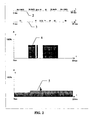
- Figure 1 represents the shape of the grey level restored by the driver as a function of the number of excited cells and may be likened to the current response of a line driver as a function of this circuit's load.
- the abscissa axis x represents the number of excited cells in the line relative to the total number of cells in the line and the ordinate axis y, the value of the grey level restored by the driver relative to that restored for a driver load of nearly 0.
- the overbrightness phenomenon appears when the temporal distribution of the load is not uniform. For example, for an addressing on 8 sub-scans, if, in one frame period, the first 10 milliseconds are used to address the low-order sub-scans and the other 10 milliseconds the high-order sub-scan and if the relevant line contains 10% of cells receiving a coding level of 127 and 80% a level of 128, then the 127 level will be restored to 75% of its value and the 128 level to only 32%. Globally, the 10% of cells at the 127 level will appear brighter than the 80% of cells at the 128 level, hence the concept of overbrightness.
- the video is generally quantized on 8 bits. Given the present-day characteristics of plasma panels (Nl) and of the time required to address a line (t ad ), it is nowadays possible to perform up to 10 sub-scans in less than 20 ms.
- the basic idea of the invention consists in employing a larger number of sub-scans than that required for coding the video, for example 10 sub-scans, and in utilizing the various possibilities for retranscribing the 256 levels, that is to say the various possible sub-scan combinations for a given value to be coded.
- a variant of the invention consists in coding the levels of the digital video signal in a special notation rather than in the notation to the base two so as better to distribute the load over the duration of a frame. It is thus possible to choose a code whose successive weights do not follow this geometric progression with common ratio 2 and which allows several combinations for the coding of one and the same value.
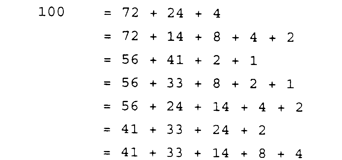
- An example of a code which assigns a weight other than a power of 2 to some of the bits of the binary coding word could for example consist of the following string of values: 1 2 4 8 14 24 33 41 56 72, the sum of all these weights (corresponding to place values 1 to 10 of the binary coding word) still being 255.
- the abscissa axis for curves 2, 3, 4 and 5, represents the timescale t and the graduation on this axis the temporal distribution of the codes. These graduations are therefore durations which depend on the weights allocated to the various sub-scans making up the binary word.
- Curve 2 an axis graduated according to a temporal distribution of the weights in powers of two, in fact represents the abscissa axis of curve 4.
- This axis 2 is labelled with the values to the power of two corresponding to the weights of the column control words.
- the values 64 and 128 divided by two so as to indicate that these values 64 and 128 are, as indicated earlier in the description of the nearest prior art, distributed over two sub-scans.
- Curve 3 an axis graduated according to a temporal distribution of weights which are not necessarily powers of two, in fact represents the abscissa axis of curve 5. This axis 3 is labelled with the values corresponding to the weights of the example above.
- Curve 4 represents the temporal distribution of the load of a driver over a line, in the case of the prior art, the line being made up 70% by the value 100 and 30% by the value 0.
- the abscissa axis is the time axis and the ordinate axis represents the percentage of load of the line.
- Curve 5 represents the temporal distribution of the load of a driver over a line, when the invention is employed, the line still being made up 70% by the value 100 and 30% by the value 0.
- the abscissa axis is the time axis and the ordinate axis represents the percentage of load of the line.
- Figure 3 represents a simplified diagram of the control circuits of a plasma panel 6.
- the digital video information arrives at the input E of the device which is also the input of a video processing circuit 7.
- This circuit is connected to a correspondence memory 8 and the input of a video memory 9 which will transmit the stored information to the input of a circuit 10 which groups together the column drivers.
- a scan generator 11 transmits synchronization information to the video memory 9 and controls a circuit 12 which groups together the line drivers.
- the video information coded on 8 bits and received on the input E of the device is thus processed by the processor.
- the latter exchanges these data with the memory or correspondence table 8 which, depending on the values of the video words sent as addresses, will deliver as data, words coded on 10 bits whose weights will have been defined beforehand.
- These words are then transmitted to the video memory 9 which stores them so as to deliver the successive bits of the column control words to the column drivers, in synchronization with the line scan.
- the scan generator 11 carries out, for the duration of a frame and by way of the line driver circuits 12, ten sub-scans of the display, each sub-scan corresponding to one bit of the column control word.
- the circuit 12 delivers the addressing voltage and also the holding voltage for the duration corresponding to the weight of the sub-scan sent on the columns during this addressing.
- the choice of the column control word for a grey level to be coded and for a given column can be made in a specified manner in such a way as to distribute the load of the line driver over the duration of a frame, although it is also possible to make this choice randomly from among all the coding possibilities.
- One solution adopted consists in selecting the word which possesses the most 1 bits and, from among these words, the one whose high-order 1 bit has the smallest weight, while considering the lower high-order bits if there is equality. By virtue of this selection, the load of the driver is distributed over the maximum number of bits, thus diminishing the overbrightness effects. The choosing of the least weight makes it possible moreover to diminish the contour effects, better known as "contouring”.
- the hardware construction is also simplified since its solution does not require the generation of a random code.
- the invention is not limited by the number of bits which quantize the digital video signal to be displayed, nor the number of sub-scans.
- micromirrors reflect received light in a point-wise manner when they are selected.
- the micromirrors which are therefore cells, in the broad sense of the term, arranged as a matrix array having line inputs and column inputs, are then addressed in the same way as the cells of plasma panels.
Landscapes
- Engineering & Computer Science (AREA)
- Physics & Mathematics (AREA)
- Computer Hardware Design (AREA)
- General Physics & Mathematics (AREA)
- Theoretical Computer Science (AREA)
- Control Of Indicators Other Than Cathode Ray Tubes (AREA)
- Control Of Gas Discharge Display Tubes (AREA)
- Transforming Electric Information Into Light Information (AREA)
Abstract
Description
- Figure 1, the luminance level restored by the driver as a function of the percentage of cells excited in the line,
- Figure 2, the temporal distribution of the load over a line according to the prior art and according to the invention,
- Figure 3, a simplified diagram of the control circuits of a plasma panel.
1 2 4 8 14 24 33 41 56 72,
the sum of all these weights (corresponding to
Claims (8)
- Process for addressing cells of a plasma panel arranged as a matrix array, each cell being situated at the intersection of a line and a column, the array having line inputs and column inputs for displaying grey levels defined by video words making up a digital video signal, the column inputs each receiving a control word for this column corresponding to the video word relating, for this column, to the addressed line, this word being made up of n bits transmitted sequentially, each bit triggering or not triggering, depending on its state, the selection of the cell of the addressed line and of the corresponding column for a time proportional to the weight of this bit within the word, characterized in that it comprises a step effecting a transcoding of the video words into column control words such that the number of bits of the column control words is greater than that of the video words and such that different column control words are used for coding the same grey level of the video signal.
- Process according to Claim 1, characterized in that at least one of the weights of the column control words is different from a power of two.
- Process according to Claim 1 or 2, characterized in that the video coding is performed on 8 bits, the column control words are 10-bit words and the various weights assigned to these control words are computed in such a way that the mean number of combinations over the set of grey levels is a maximum.
- Process according to Claim 1, 2 or 3, characterized in that the sum of the weights of the column control word is equal to the sum for the video word.
- Process according to Claim 1, 2, 3 or 4, characterized in that the column control words are chosen, for a given line and when several combinations are possible, randomly from among the various possibilities.
- Process according to Claim 1, 2, 3 or 4, characterized in that the column control words chosen, when a choice is possible, are those having the most one bits.
- Process according to Claim 6, characterized in that the control words chosen, when a choice is possible, are those for which the value of the highest weight at one is the smallest.
- Device for addressing a plasma panel (6) for the implementation of the process according to Claim 1, comprising a video processing circuit (7) for processing the digital video data received, a correspondence memory (8) for transcoding these data, a video memory (9) for storing the transcoded data, the video memory being linked to column driver circuits (10) in order to control the column addressing of the plasma panel, characterized in that the transcoded data have a greater number of bits than the digital video data received and in that the processing circuit (7) comprises means for differently coding identical values of digital video data received.
Applications Claiming Priority (2)
| Application Number | Priority Date | Filing Date | Title |
|---|---|---|---|
| FR9705165A FR2762703B1 (en) | 1997-04-25 | 1997-04-25 | ROTARY CODE ADDRESSING METHOD AND DEVICE FOR PLASMA SCREENS |
| FR9705165 | 1997-04-25 |
Publications (2)
| Publication Number | Publication Date |
|---|---|
| EP0874348A1 true EP0874348A1 (en) | 1998-10-28 |
| EP0874348B1 EP0874348B1 (en) | 2008-12-31 |
Family
ID=9506332
Family Applications (1)
| Application Number | Title | Priority Date | Filing Date |
|---|---|---|---|
| EP98400796A Expired - Lifetime EP0874348B1 (en) | 1997-04-25 | 1998-04-03 | Process and device for addressing of a plasma display with diverse codes |
Country Status (6)
| Country | Link |
|---|---|
| US (1) | US6404440B1 (en) |
| EP (1) | EP0874348B1 (en) |
| JP (2) | JP4393600B2 (en) |
| KR (1) | KR100521340B1 (en) |
| DE (1) | DE69840392D1 (en) |
| FR (1) | FR2762703B1 (en) |
Cited By (3)
| Publication number | Priority date | Publication date | Assignee | Title |
|---|---|---|---|---|
| WO2001022395A1 (en) * | 1999-09-17 | 2001-03-29 | Koninklijke Philips Electronics N.V. | Method of and unit for displaying an image in sub-fields |
| EP1111573A1 (en) * | 1999-12-22 | 2001-06-27 | THOMSON multimedia | Method of addressing a plasma display panel |
| EP0884717B1 (en) * | 1997-06-13 | 2003-09-17 | Matsushita Electric Industrial Co., Ltd. | Method and apparatus for correcting image distortion for a plasma display panel using minimum MPD distance code |
Families Citing this family (9)
| Publication number | Priority date | Publication date | Assignee | Title |
|---|---|---|---|---|
| EP1049068A1 (en) * | 1999-04-28 | 2000-11-02 | THOMSON multimedia S.A. | Method and apparatus for processing video signals |
| KR100831234B1 (en) | 2002-04-01 | 2008-05-22 | 삼성전자주식회사 | A method for a frame rate control and a liquid crystal display for the method |
| EP1359749A1 (en) * | 2002-05-04 | 2003-11-05 | Deutsche Thomson-Brandt Gmbh | Multiscan display mode for a plasma display panel |
| US7626635B2 (en) * | 2003-04-04 | 2009-12-01 | Koplar Interactive Systems International, L.L.C. | Method and system of detecting signal presence from a video signal presented on a digital display device |
| US7974435B2 (en) * | 2005-09-16 | 2011-07-05 | Koplar Interactive Systems International Llc | Pattern-based encoding and detection |
| US7974438B2 (en) * | 2006-12-11 | 2011-07-05 | Koplar Interactive Systems International, Llc | Spatial data encoding and decoding |
| US20080198923A1 (en) * | 2007-01-05 | 2008-08-21 | Gramelspacher Michael S | Content signal modulation and decoding |
| US8798133B2 (en) * | 2007-11-29 | 2014-08-05 | Koplar Interactive Systems International L.L.C. | Dual channel encoding and detection |
| TWI417862B (en) * | 2009-11-30 | 2013-12-01 | Innolux Corp | Liquid crystal display and driving method thereof |
Citations (2)
| Publication number | Priority date | Publication date | Assignee | Title |
|---|---|---|---|---|
| EP0674303A2 (en) * | 1990-11-28 | 1995-09-27 | Fujitsu Limited | A circuit for gradationally driving a flat display device |
| EP0698874A1 (en) * | 1994-07-25 | 1996-02-28 | Texas Instruments Incorporated | Method for reducing temporal artifacts in digital video systems |
Family Cites Families (12)
| Publication number | Priority date | Publication date | Assignee | Title |
|---|---|---|---|---|
| FR674303A (en) * | 1929-04-30 | 1930-01-27 | Ingersoll Rand Co | Lubricators for air lines |
| JP2720607B2 (en) * | 1990-03-02 | 1998-03-04 | 株式会社日立製作所 | Display device, gradation display method, and drive circuit |
| GB9024978D0 (en) * | 1990-11-16 | 1991-01-02 | Rank Cintel Ltd | Digital mirror spatial light modulator |
| JP3489884B2 (en) * | 1994-02-08 | 2004-01-26 | 富士通株式会社 | In-frame time division display device and halftone display method in in-frame time division display device |
| US5619228A (en) * | 1994-07-25 | 1997-04-08 | Texas Instruments Incorporated | Method for reducing temporal artifacts in digital video systems |
| EP0837441B1 (en) * | 1995-04-07 | 2005-01-26 | Fujitsu General Limited | Method of driving display device |
| JP3499058B2 (en) * | 1995-09-13 | 2004-02-23 | 富士通株式会社 | Driving method of plasma display and plasma display device |
| US6100939A (en) * | 1995-09-20 | 2000-08-08 | Hitachi, Ltd. | Tone display method and apparatus for displaying image signal |
| JPH09107512A (en) * | 1995-10-13 | 1997-04-22 | Hitachi Ltd | Gradation display method for television image signal |
| JPH0997035A (en) * | 1995-09-29 | 1997-04-08 | Fujitsu General Ltd | Display device drive method |
| CA2187044C (en) * | 1995-10-06 | 2003-07-01 | Vishal Markandey | Method to reduce perceptual contouring in display systems |
| JP3328134B2 (en) * | 1996-05-23 | 2002-09-24 | 富士通株式会社 | In-frame time division type halftone display method and in-frame time division type display device |
-
1997
- 1997-04-25 FR FR9705165A patent/FR2762703B1/en not_active Expired - Fee Related
-
1998
- 1998-04-03 DE DE69840392T patent/DE69840392D1/en not_active Expired - Lifetime
- 1998-04-03 EP EP98400796A patent/EP0874348B1/en not_active Expired - Lifetime
- 1998-04-15 JP JP10496298A patent/JP4393600B2/en not_active Expired - Fee Related
- 1998-04-16 US US09/061,418 patent/US6404440B1/en not_active Expired - Lifetime
- 1998-04-20 KR KR1019980014038A patent/KR100521340B1/en not_active IP Right Cessation
-
2009
- 2009-01-06 JP JP2009000634A patent/JP2009069859A/en active Pending
Patent Citations (2)
| Publication number | Priority date | Publication date | Assignee | Title |
|---|---|---|---|---|
| EP0674303A2 (en) * | 1990-11-28 | 1995-09-27 | Fujitsu Limited | A circuit for gradationally driving a flat display device |
| EP0698874A1 (en) * | 1994-07-25 | 1996-02-28 | Texas Instruments Incorporated | Method for reducing temporal artifacts in digital video systems |
Cited By (6)
| Publication number | Priority date | Publication date | Assignee | Title |
|---|---|---|---|---|
| EP0884717B1 (en) * | 1997-06-13 | 2003-09-17 | Matsushita Electric Industrial Co., Ltd. | Method and apparatus for correcting image distortion for a plasma display panel using minimum MPD distance code |
| WO2001022395A1 (en) * | 1999-09-17 | 2001-03-29 | Koninklijke Philips Electronics N.V. | Method of and unit for displaying an image in sub-fields |
| KR100742519B1 (en) * | 1999-09-17 | 2007-08-02 | 코닌클리케 필립스 일렉트로닉스 엔.브이. | Method of and unit for displaying an image in sub-fields |
| EP1111573A1 (en) * | 1999-12-22 | 2001-06-27 | THOMSON multimedia | Method of addressing a plasma display panel |
| FR2803076A1 (en) * | 1999-12-22 | 2001-06-29 | Thomson Multimedia Sa | PLASMA DISPLAY PANEL ADDRESSING METHOD |
| US6747670B2 (en) | 1999-12-22 | 2004-06-08 | Thomson Licensing S.A. | Method of addressing a plasma display panel |
Also Published As
| Publication number | Publication date |
|---|---|
| FR2762703B1 (en) | 1999-07-16 |
| EP0874348B1 (en) | 2008-12-31 |
| KR19980081551A (en) | 1998-11-25 |
| JP4393600B2 (en) | 2010-01-06 |
| FR2762703A1 (en) | 1998-10-30 |
| JPH1130970A (en) | 1999-02-02 |
| DE69840392D1 (en) | 2009-02-12 |
| KR100521340B1 (en) | 2006-01-12 |
| JP2009069859A (en) | 2009-04-02 |
| US6404440B1 (en) | 2002-06-11 |
Similar Documents
| Publication | Publication Date | Title |
|---|---|---|
| EP0874349B1 (en) | Process for adressing bits on more than one line of a plasma display | |
| US6127991A (en) | Method of driving flat panel display apparatus for multi-gradation display | |
| JP2009069859A (en) | Device and method for rotating-code addressing for plasma display | |
| US7773161B2 (en) | Method and apparatus for controlling a display device | |
| KR100934952B1 (en) | Method and apparatus for processing video pictures, especially for improving grey scale fidelity portrayal | |
| EP0919984B1 (en) | Process and device for scanning a plasma panel | |
| EP0945846B1 (en) | Process and device for addressing a plasma display panel | |
| EP1353315A1 (en) | Method and apparatus for processing video pictures to improve grey scale resolution of a display device | |
| JP2003015594A (en) | Circuit and method for coding subfield | |
| EP1260957B1 (en) | Pre-filtering for a Plasma Display Panel Signal | |
| US20050093775A1 (en) | Method of driving a plasma display panel | |
| JP2005516243A (en) | Display panel cell address | |
| KR100669274B1 (en) | Method of driving flat panel display apparatus | |
| KR100452386B1 (en) | The operating method for ac plasma display panel | |
| KR100427744B1 (en) | Method for data interface of plasma display panel | |
| EP1684258A1 (en) | Method and apparatus for displaying video images on a plasma display panel | |
| JP2000242226A (en) | Gray level display method and display device | |
| KR19980074917A (en) | A driving method of a plasma display device and a driving circuit thereof | |
| KR19980075737A (en) | The driving circuit of the plasma display device |
Legal Events
| Date | Code | Title | Description |
|---|---|---|---|
| PUAI | Public reference made under article 153(3) epc to a published international application that has entered the european phase |
Free format text: ORIGINAL CODE: 0009012 |
|
| AK | Designated contracting states |
Kind code of ref document: A1 Designated state(s): DE FR GB IT |
|
| AX | Request for extension of the european patent |
Free format text: AL;LT;LV;MK;RO;SI |
|
| 17P | Request for examination filed |
Effective date: 19990420 |
|
| AKX | Designation fees paid |
Free format text: AT BE CH CY LI |
|
| RBV | Designated contracting states (corrected) |
Designated state(s): DE FR GB IT |
|
| REG | Reference to a national code |
Ref country code: DE Ref legal event code: 8566 |
|
| 17Q | First examination report despatched |
Effective date: 20050929 |
|
| GRAP | Despatch of communication of intention to grant a patent |
Free format text: ORIGINAL CODE: EPIDOSNIGR1 |
|
| RAP1 | Party data changed (applicant data changed or rights of an application transferred) |
Owner name: THOMSON LICENSING, S.A. |
|
| GRAS | Grant fee paid |
Free format text: ORIGINAL CODE: EPIDOSNIGR3 |
|
| GRAA | (expected) grant |
Free format text: ORIGINAL CODE: 0009210 |
|
| AK | Designated contracting states |
Kind code of ref document: B1 Designated state(s): DE FR GB IT |
|
| REG | Reference to a national code |
Ref country code: GB Ref legal event code: FG4D |
|
| REF | Corresponds to: |
Ref document number: 69840392 Country of ref document: DE Date of ref document: 20090212 Kind code of ref document: P |
|
| PLBE | No opposition filed within time limit |
Free format text: ORIGINAL CODE: 0009261 |
|
| STAA | Information on the status of an ep patent application or granted ep patent |
Free format text: STATUS: NO OPPOSITION FILED WITHIN TIME LIMIT |
|
| 26N | No opposition filed |
Effective date: 20091001 |
|
| PGFP | Annual fee paid to national office [announced via postgrant information from national office to epo] |
Ref country code: GB Payment date: 20140428 Year of fee payment: 17 |
|
| PGFP | Annual fee paid to national office [announced via postgrant information from national office to epo] |
Ref country code: IT Payment date: 20140422 Year of fee payment: 17 Ref country code: FR Payment date: 20140418 Year of fee payment: 17 Ref country code: DE Payment date: 20140425 Year of fee payment: 17 |
|
| REG | Reference to a national code |
Ref country code: DE Ref legal event code: R119 Ref document number: 69840392 Country of ref document: DE |
|
| GBPC | Gb: european patent ceased through non-payment of renewal fee |
Effective date: 20150403 |
|
| PG25 | Lapsed in a contracting state [announced via postgrant information from national office to epo] |
Ref country code: DE Free format text: LAPSE BECAUSE OF NON-PAYMENT OF DUE FEES Effective date: 20151103 Ref country code: IT Free format text: LAPSE BECAUSE OF NON-PAYMENT OF DUE FEES Effective date: 20150403 Ref country code: GB Free format text: LAPSE BECAUSE OF NON-PAYMENT OF DUE FEES Effective date: 20150403 |
|
| REG | Reference to a national code |
Ref country code: FR Ref legal event code: ST Effective date: 20151231 |
|
| PG25 | Lapsed in a contracting state [announced via postgrant information from national office to epo] |
Ref country code: FR Free format text: LAPSE BECAUSE OF NON-PAYMENT OF DUE FEES Effective date: 20150430 |