EP0873533B1 - Wavelength multiplexer/demultiplexer with varied propagation constant - Google Patents
Wavelength multiplexer/demultiplexer with varied propagation constant Download PDFInfo
- Publication number
- EP0873533B1 EP0873533B1 EP97902828A EP97902828A EP0873533B1 EP 0873533 B1 EP0873533 B1 EP 0873533B1 EP 97902828 A EP97902828 A EP 97902828A EP 97902828 A EP97902828 A EP 97902828A EP 0873533 B1 EP0873533 B1 EP 0873533B1
- Authority
- EP
- European Patent Office
- Prior art keywords
- waveguides
- wavefronts
- optical
- core
- propagation
- Prior art date
- Legal status (The legal status is an assumption and is not a legal conclusion. Google has not performed a legal analysis and makes no representation as to the accuracy of the status listed.)
- Expired - Lifetime
Links
Images
Classifications
-
- G—PHYSICS
- G02—OPTICS
- G02B—OPTICAL ELEMENTS, SYSTEMS OR APPARATUS
- G02B6/00—Light guides; Structural details of arrangements comprising light guides and other optical elements, e.g. couplings
- G02B6/10—Light guides; Structural details of arrangements comprising light guides and other optical elements, e.g. couplings of the optical waveguide type
- G02B6/12—Light guides; Structural details of arrangements comprising light guides and other optical elements, e.g. couplings of the optical waveguide type of the integrated circuit kind
- G02B6/12007—Light guides; Structural details of arrangements comprising light guides and other optical elements, e.g. couplings of the optical waveguide type of the integrated circuit kind forming wavelength selective elements, e.g. multiplexer, demultiplexer
- G02B6/12009—Light guides; Structural details of arrangements comprising light guides and other optical elements, e.g. couplings of the optical waveguide type of the integrated circuit kind forming wavelength selective elements, e.g. multiplexer, demultiplexer comprising arrayed waveguide grating [AWG] devices, i.e. with a phased array of waveguides
- G02B6/12011—Light guides; Structural details of arrangements comprising light guides and other optical elements, e.g. couplings of the optical waveguide type of the integrated circuit kind forming wavelength selective elements, e.g. multiplexer, demultiplexer comprising arrayed waveguide grating [AWG] devices, i.e. with a phased array of waveguides characterised by the arrayed waveguides, e.g. comprising a filled groove in the array section
-
- G—PHYSICS
- G02—OPTICS
- G02B—OPTICAL ELEMENTS, SYSTEMS OR APPARATUS
- G02B6/00—Light guides; Structural details of arrangements comprising light guides and other optical elements, e.g. couplings
- G02B6/10—Light guides; Structural details of arrangements comprising light guides and other optical elements, e.g. couplings of the optical waveguide type
- G02B6/12—Light guides; Structural details of arrangements comprising light guides and other optical elements, e.g. couplings of the optical waveguide type of the integrated circuit kind
- G02B6/12007—Light guides; Structural details of arrangements comprising light guides and other optical elements, e.g. couplings of the optical waveguide type of the integrated circuit kind forming wavelength selective elements, e.g. multiplexer, demultiplexer
- G02B6/12009—Light guides; Structural details of arrangements comprising light guides and other optical elements, e.g. couplings of the optical waveguide type of the integrated circuit kind forming wavelength selective elements, e.g. multiplexer, demultiplexer comprising arrayed waveguide grating [AWG] devices, i.e. with a phased array of waveguides
- G02B6/12014—Light guides; Structural details of arrangements comprising light guides and other optical elements, e.g. couplings of the optical waveguide type of the integrated circuit kind forming wavelength selective elements, e.g. multiplexer, demultiplexer comprising arrayed waveguide grating [AWG] devices, i.e. with a phased array of waveguides characterised by the wavefront splitting or combining section, e.g. grooves or optical elements in a slab waveguide
Definitions
- the invention relates to an apparatus for multiplexing or demultiplexing optical signals according to their wavelength.
- Optical signals of different wavelengths traveling in separate optical fibers can be routed into a single optical fiber by a wavelength multiplexer and later rerouted into separate optical fibers by a wavelength demultiplexer.
- the devices used in multiplexing and demultiplexing operations must be reversible so the same devices function as multiplexers in one direction of travel and as demultiplexers in the opposite direction of travel.
- the dispersing function spatially distinguishes the different wavelength signals, referred to as channels; and the focusing function routes the signals between input and output waveguides according to their dispersion.
- some multiplexing and demultiplexing devices use reflective diffraction gratings to both disperse and focus the signals. Diffraction is the mechanism of dispersion, and grating curvature provides the focus.
- Other such devices referred to as "phasors" interconnect input and output waveguides with a plurality of central waveguides that vary progressively in length. The progressive variation in waveguide length produces phase front tilt as a function of wavelength. An angular arrangement of the central waveguides provides the focus.
- dispersing components can be simplified.
- flat diffraction gratings can be used in place of curved diffraction gratings, or parallel central waveguides can be used in place of angularly arrayed central waveguides.
- my invention uses a progressive change in propagation constant to provide the dispersive function in wavelength multiplexers and demultiplexers.
- This new mechanism for accomplishing wavelength dispersion can be used to reduce the physical size and simplify the fabrication of these devices.
- An apparatus for multiplexing or demultiplexing optical signals according to their wavelength is defined in claim 1.
- a method of dispersing different wavelength signals, according to the invention, is defined in claim 36.
- An embodiment of my invention includes the usual features of input and output optical pathways interconnected by dispersing and focusing elements.
- the input optical pathway conveys a plurality of channels distinguished by wavelength
- the output optical pathways separately convey the channels.
- the dispersing element is a central optical pathway that receives the plurality of channels from the input optical pathway as a plurality of parallel wavefronts and transforms the plurality of parallel wavefronts into a plurality of relatively inclined wavefronts.
- the focusing element directs the relatively inclined wavefronts along the different output optical pathways.
- the central pathway of my invention exhibits different propagation constants for a given wavelength across the central waveguide in a direction transverse to the direction of wave forum propagation through the central waveguide.
- the propagation constants can be changed in various ways. These include changing core dimensions of the central waveguide, as well as changing the index values of the core and cladding.
- the index profile of the core also figures in the propagation constant of non-step index profiles. For example, the index profile can be selected to increase the rate of change of the propagation constant for a given change in core dimension or peak refractive indices.
- the central pathway can be composed of either a plurality of individual waveguides (or optical fibers) or a common waveguide. Both include core portions surrounded by cladding. Core portions of the individual waveguides can be varied in width, thickness, and cross-sectional shape; and the core portion of the common waveguide can be varied in thickness. The overcladding can also be varied in thickness. Doping or other material variations can be used to change the index values of the core and cladding between the individual waveguides or across the common waveguide.
- a reflective optic is positioned at one end of the central pathway to provide a more compact design.
- the relatively inclined wavefronts of the different wavelengths are further relatively inclined within the same space of the central pathway by retroreflection through the central pathway.
- the input and output pathways are adjacent to each other.
- the focusing element preferably performs a collimating function for directing different portions of the wavefronts along parallel optical pathways.
- the reflective optic for retroreflecting the wavefronts along the parallel optical pathways is flat, and the individual waveguides of the central pathway are parallel to each other.
- the parallel pathways can also extend through the common waveguide without any lateral divisions, because the light remains collimated in the direction of propagation.
- optical pathways and the dispersing and focusing elements are preferably formed as an integrated optical circuit in planar optics.
- the relatively simple design of the elements allows for the use of fabrication techniques such as "redraw", where more exact tolerances can be obtained by stretching planar substrates to control thickness.
- the invention could also be implemented in bulk optics or in a combination of planar and bulk optics.
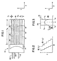
- FIG. 1 is a plan view of a new demultiplexing optic in planar form having a plurality of parallel waveguides for dispersing different wavelength signals.
- FIG. 2 is a graph showing phase front tilt to two different wavelengths measured across a central passageway of the optic.
- FIG. 3 is a graph showing an index profile superimposed on a section of waveguide.
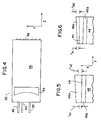
- FIG. 4 is a plan view of a second demultiplexing device having a common waveguide for dispersing different wavelength signals.
- FIG. 5 is a cross-sectional end view of the common waveguide showing a tapered core layer.
- FIG. 6 is a cross-sectional end view of the common waveguide showing a tapered cladding layer.
- FIG. 7 is a plan view of a third demultiplexing device having a common waveguide with varying concentrations of dopant for dispersing different wavelength signals.
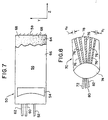
- FIG. 8 is a plan view of a fourth demultiplexing device having a plurality of radial waveguides for dispersing different wavelength signals.
- FIGS. 1-3 Illustrated by drawing FIGS. 1-3 is a first embodiment of my invention implemented in planar optics.
- the embodiment is described with respect to a direction of light travel for a demultiplexer but could function equally well in the opposite direction of light travel as a multiplexer.
- the terms "multiplexer” and "demultiplexer” are used only for the purpose of referencing the embodiment to one of these possible functions but do not exclude the other.
- Optical signals of differing wavelengths enter a planar demultiplexing optic 10 from an input waveguide (or optical fiber) 12 and diverge to fill the aperture of a focusing optic (collimating lens) 14.
- the diverging wavefronts are collimated by the focusing optic 14.
- Discrete portions of the wavefronts propagate through a plurality of parallel waveguides 16 to a flat reflective optic 18, which retroreflects the wavefronts on a return path to the focusing optic 14.
- the input waveguide 12 is preferably located along an optical axis of the focusing optic 14, but similar principles also apply for off-axis arrangements.
- the change in optical path lengths "L i " evaluated at the reflective optic 18 relatively inclines the wavefronts according to their wavelengths ⁇ 1 - ⁇ n as shown in the graph of FIG. 2.
- the graph ordinate spans the waveguides 16 in the direction "Y" at a position coincident with the reflective optic 18.
- the graph abscissa is in units of phase angle " ⁇ ".
- the stepped line ⁇ ( ⁇ 1 ) represents a collection of the phase angles " ⁇ " in the waveguides 16 for the wavelength ⁇ 1 .
- the stepped line ⁇ ( ⁇ n ) represents a collection of the phase angles " ⁇ " in the waveguides 16 for the wavelength ⁇ n .
- the angular difference between the two stepped lines ⁇ ( ⁇ 1 ) and ⁇ ( ⁇ n ) represents a difference in phase front tilt between the two wavelengths ⁇ 1 and ⁇ n .
- the phase front tilt changes the focus of the returning wavefronts from coincidence with the input waveguide 12 (the expected focus of retroreflected wavefronts that are not tilted) to output waveguides 20 and 22 according to the respective amounts of tilt.
- the wavelength ⁇ 1 focuses on the closer output waveguide 20 and the wavelength ⁇ n focuses on the more distant output waveguide 22.
- more wavelengths ⁇ between the wavelengths ⁇ 1 and ⁇ n representing additional signals (or channels), could be focused on additional output waveguides positioned between the waveguides 20 and 22.
- the number of waveguides 16 could be increased to more accurately image the mode field of the input waveguide 12 on each of the output waveguides 20 and 22.
- n eff ⁇ k 0
- k 0 2 ⁇ ⁇
- the propagation constant " ⁇ " can be calculated from a wave equation using well-known techniques.
- An example of a wave equation for a planar optical waveguide found in a reference by J. P. Meunier et al., Optical and Quantum Electronics 15, (1983) 77-85, is as follows: where the term “ ⁇ m (x)" is a field distribution of the mode and "n(x)'' is the index profile of the core.
- the index profile "n(x)" which is shown in the cross-sectional view of FIG. 3, depends on the profile shape, core dimension "a”, and the peak index values "n 0 " of core 24 and "n clad " of cladding 26.
- the latter peak index values "n 0 " and "n clad " are often considered together as the variable " ⁇ ", which is defined as follows: ⁇ n 0 - n clad n 0
- any of these variables that affect the index profile "n(x)" of the respective waveguides 16 also can be used to change the propagation constant " ⁇ ", which in turn changes the effective index "n eff " and the resulting optical path length "L i " of the waveguides 16.
- the progressive variation in optical path length "L i " of the waveguides 16 in the "Y” direction produces the different wavefront tilts of the wavelength ⁇ 1 and ⁇ n , causing them to focus in the different positions occupied by the output waveguides 20 and 22.
- the profile shape of non-step index waveguide profiles is adjusted so that changes in the waveguide dimensions, e.g., "a”, or changes in the peak indices, e.g., " ⁇ ", produce larger changes in the propagation constant " ⁇ ". This limits the amount of required physical change between the different waveguides 16.
- the waveguides are preferably single mode to better control differences between their optical path lengths "L i ".
- FIGS. 4-6 Two versions of a second embodiment of my invention are illustrated in FIGS. 4-6.
- a new planar demultiplexing optic 30 includes several of the same components as the planar optic 10 including input waveguide 32, collimating optic 34, reflecting optic 38, and output waveguides 40 and 42.
- the plurality of individual waveguides 16 are replaced by a common waveguide 36.
- a thickness dimension "t" of the common waveguide 36 is varied in the same "Y” direction transverse to the direction "Z" of wavefront propagation.
- the common waveguide 36 is formed by a continuous layer 44 of core material located between continuous layers 46a and 46b of cladding material on a planar substrate 48.
- the core layer 44 continuously varies in thickness from “t a1 " to "t a2 " across the common waveguide 36.
- the cladding layer 46a varies in thickness from "t b1 " to "t b2 " across the common waveguide 36.
- Both thickness variations result in a continuous change of the propagation constant " ⁇ " in the "Y” direction across the waveguide.
- the collimating optic 34 limits any movement of the propagating wavefronts in the "Y” direction, so individual waveguides are not required to separate the propagating wavefronts into separate paths having different optical path lengths "L i ".
- the continuous variation of the propagation constant " ⁇ " is expected to more accurately project the mode field of the input waveguide 32 on each of the output waveguides 40 and 42.
- planar multiplexing optics 10 and 30 are particularly suitable for simplified manufacture by "redraw” in which layers of core 44 and cladding 46a and 46b are deposited on the substrate 48 with additional thickness and are stretched together with the substrate to exact dimensions. The process permits much wider tolerances for deposition. Alternatively, grinding or polishing could be used to control waveguide thickness.
- a third embodiment of my invention illustrated in FIG. 7, includes several features in common with the second embodiment.
- a planar demultiplexing optic 50 includes an input waveguide 52, a focusing optic (collimating lens) 54, a common waveguide 56, a flat reflective optic 58, and output waveguides 60 and 62.
- the propagation constant " ⁇ " is varied by a change of refractive index across the common waveguide 56.
- the peak refractive indices of the core 64 and cladding 66 can be changed, such as by adding varying concentrations of dopant 68.
- the result is similar to the second embodiment, namely, a continuous variation in the optical path length in the "Y" direction.
- the change in refractive index can be made in several ways including using a thin film approach such as OVD (outside vapor deposition) and PECVD (plasma-enhanced chemical vapor deposition).
- OVD outside vapor deposition
- PECVD plasma-enhanced chemical vapor deposition
- the varying concentrations of dopant 68 could also be achieved using ion exchange techniques.
- a fourth and final embodiment shown in FIG. 8 is formed as a planar demultiplexing optic 70 including an input waveguide 72 and a focusing optic 74, which has zero power but provides a free-space region for converging or diverging wavefronts.
- a periodic array of radial waveguides 76 which form a central pathway through the optic 70, terminate at a curved reflective optic 78.
- Each radial waveguide 76 conveys a separate portion of a respective cylindrical wavefront corresponding to one of the wavelengths " ⁇ 1 " through " ⁇ n ".
- the curved reflective optic 78 retroreflects the cylindrical wavefronts on a converging path through the radial waveguides 76 to the free-space of the focusing optic 74.
- the radial waveguides 76 progressively vary in width from “a 1 " to "a n” for changing the propagation constant " ⁇ " of different portions of the cylindrical wavefronts.
- the wavefronts of the different wavelengths " ⁇ 1 " through “ ⁇ n " propagate cylindrically, the change in propagation constant " ⁇ ” remains transverse to the instant directions of wavefront propagation along the radial waveguides 76.
- the resulting change in the optical path lengths "L i " of the radial waveguides 76 relatively inclines the cylindrical wavefronts of the different wavelengths " ⁇ 1 " through “ ⁇ n “, causing them to converge to slightly different focus positions at output waveguides 80 and 82.
- the waveguides in the illustrated embodiments have been depicted as buried waveguides, but other known types of waveguides including rib waveguides could also be used.
- the focusing optic which has been depicted as a lens, could also be arranged together with the input or output waveguides as a mirror, such as a collimating mirror or similar reflective surface.
- the input and output waveguides of the various embodiments could also be arrayed in various combinations including equal numbers of input and output waveguides.
Description
- The invention relates to an apparatus for multiplexing or demultiplexing optical signals according to their wavelength.
- Optical signals of different wavelengths traveling in separate optical fibers can be routed into a single optical fiber by a wavelength multiplexer and later rerouted into separate optical fibers by a wavelength demultiplexer. Generally, the devices used in multiplexing and demultiplexing operations must be reversible so the same devices function as multiplexers in one direction of travel and as demultiplexers in the opposite direction of travel.
- Within the multiplexing and demultiplexing devices, two main functions are performed, namely, dispersing and focusing. The dispersing function spatially distinguishes the different wavelength signals, referred to as channels; and the focusing function routes the signals between input and output waveguides according to their dispersion.
- Often, the same optical components perform both functions. For example, some multiplexing and demultiplexing devices use reflective diffraction gratings to both disperse and focus the signals. Diffraction is the mechanism of dispersion, and grating curvature provides the focus. Other such devices referred to as "phasors" interconnect input and output waveguides with a plurality of central waveguides that vary progressively in length. The progressive variation in waveguide length produces phase front tilt as a function of wavelength. An angular arrangement of the central waveguides provides the focus.
- Alternatively, separate lenses or mirrors can be used to provide the focusing function. Relieved of this additional requirement, the dispersing components can be simplified. For example, flat diffraction gratings can be used in place of curved diffraction gratings, or parallel central waveguides can be used in place of angularly arrayed central waveguides.
- As design criteria become more stringent, such as requiring more closely spaced channels with minimum loss, lower cost, and smaller size, the current designs of multiplexers and demultiplexers become increasingly difficult and expensive to manufacture. High accuracy diffraction gratings are particularly expensive, and the amount of etching required by phasors is particularly time consuming.
- Ordinarily, care must be taken to avoid compositional variations in materials and other dimensional variations that could produce unwanted changes in the propagational characteristics of the waveguides. For example, U.S. Patent 5,450,511 to Dragone teaches that changes in the propagation constant can cause phase errors in the optical signals conveyed by multiplexing and demultiplexing devices resulting in increased cross-talk between channels and reduced efficiency of the devices. Moreover, this document discloses an apparatus of the type defined in the first part of claim 1. In the case of this prior art apparatus the optical waveguides forming the central optical pathway have different length.
- Contrary to the teaching that changes in the propagation constant are to be avoided, my invention uses a progressive change in propagation constant to provide the dispersive function in wavelength multiplexers and demultiplexers. This new mechanism for accomplishing wavelength dispersion can be used to reduce the physical size and simplify the fabrication of these devices.
- An apparatus for multiplexing or demultiplexing optical signals according to their wavelength, according to the invention, is defined in claim 1. A method of dispersing different wavelength signals, according to the invention, is defined in claim 36.
- An embodiment of my invention includes the usual features of input and output optical pathways interconnected by dispersing and focusing elements. As a demultiplexer, the input optical pathway conveys a plurality of channels distinguished by wavelength, and the output optical pathways separately convey the channels. The dispersing element is a central optical pathway that receives the plurality of channels from the input optical pathway as a plurality of parallel wavefronts and transforms the plurality of parallel wavefronts into a plurality of relatively inclined wavefronts. The focusing element directs the relatively inclined wavefronts along the different output optical pathways. However, instead of relatively inclining the wavefronts by diffraction or variable length waveguides, the central pathway of my invention exhibits different propagation constants for a given wavelength across the central waveguide in a direction transverse to the direction of wavefrunt propagation through the central waveguide.
- The propagation constants can be changed in various ways. These include changing core dimensions of the central waveguide, as well as changing the index values of the core and cladding. The index profile of the core also figures in the propagation constant of non-step index profiles. For example, the index profile can be selected to increase the rate of change of the propagation constant for a given change in core dimension or peak refractive indices.
- The central pathway can be composed of either a plurality of individual waveguides (or optical fibers) or a common waveguide. Both include core portions surrounded by cladding. Core portions of the individual waveguides can be varied in width, thickness, and cross-sectional shape; and the core portion of the common waveguide can be varied in thickness. The overcladding can also be varied in thickness. Doping or other material variations can be used to change the index values of the core and cladding between the individual waveguides or across the common waveguide.
- Preferably, a reflective optic is positioned at one end of the central pathway to provide a more compact design. The relatively inclined wavefronts of the different wavelengths are further relatively inclined within the same space of the central pathway by retroreflection through the central pathway. The input and output pathways are adjacent to each other. The focusing element preferably performs a collimating function for directing different portions of the wavefronts along parallel optical pathways. The reflective optic for retroreflecting the wavefronts along the parallel optical pathways is flat, and the individual waveguides of the central pathway are parallel to each other. However, the parallel pathways can also extend through the common waveguide without any lateral divisions, because the light remains collimated in the direction of propagation.
- The optical pathways and the dispersing and focusing elements are preferably formed as an integrated optical circuit in planar optics. The relatively simple design of the elements allows for the use of fabrication techniques such as "redraw", where more exact tolerances can be obtained by stretching planar substrates to control thickness. However, the invention could also be implemented in bulk optics or in a combination of planar and bulk optics.
- FIG. 1 is a plan view of a new demultiplexing optic in planar form having a plurality of parallel waveguides for dispersing different wavelength signals.
- FIG. 2 is a graph showing phase front tilt to two different wavelengths measured across a central passageway of the optic.
- FIG. 3 is a graph showing an index profile superimposed on a section of waveguide.
- FIG. 4 is a plan view of a second demultiplexing device having a common waveguide for dispersing different wavelength signals.
- FIG. 5 is a cross-sectional end view of the common waveguide showing a tapered core layer.
- FIG. 6 is a cross-sectional end view of the common waveguide showing a tapered cladding layer.
- FIG. 7 is a plan view of a third demultiplexing device having a common waveguide with varying concentrations of dopant for dispersing different wavelength signals.
- FIG. 8 is a plan view of a fourth demultiplexing device having a plurality of radial waveguides for dispersing different wavelength signals.
- Illustrated by drawing FIGS. 1-3 is a first embodiment of my invention implemented in planar optics. The embodiment is described with respect to a direction of light travel for a demultiplexer but could function equally well in the opposite direction of light travel as a multiplexer. In fact, the terms "multiplexer" and "demultiplexer" are used only for the purpose of referencing the embodiment to one of these possible functions but do not exclude the other.
- Optical signals of differing wavelengths (i.e., λ1 through λn) enter a planar demultiplexing optic 10 from an input waveguide (or optical fiber) 12 and diverge to fill the aperture of a focusing optic (collimating lens) 14. The diverging wavefronts are collimated by the focusing optic 14. Discrete portions of the wavefronts propagate through a plurality of parallel waveguides 16 to a flat reflective optic 18, which retroreflects the wavefronts on a return path to the focusing optic 14. The input waveguide 12 is preferably located along an optical axis of the focusing optic 14, but similar principles also apply for off-axis arrangements.
- The parallel waveguides 16, which form a central pathway through the planar optic 10, share a common length "lw" in a direction "Z" of wavefront propagation but progressively vary in width from "a1" to "an" along orthogonally related direction "Y". The change in waveguide width from "a1" to "an" indirectly varies optical path lengths "Li" of the different waveguides 16 by changing an effective refractive index "neff" according to the following relationship:
- The change in optical path lengths "Li" evaluated at the reflective optic 18 relatively inclines the wavefronts according to their wavelengths λ1 - λn as shown in the graph of FIG. 2. The graph ordinate spans the waveguides 16 in the direction "Y" at a position coincident with the reflective optic 18. The graph abscissa is in units of phase angle "". The stepped line (λ1) represents a collection of the phase angles "" in the waveguides 16 for the wavelength λ1. The stepped line (λn) represents a collection of the phase angles "" in the waveguides 16 for the wavelength λn. The angular difference between the two stepped lines (λ1) and (λn) represents a difference in phase front tilt between the two wavelengths λ1 and λn.
- The phase front tilt changes the focus of the returning wavefronts from coincidence with the input waveguide 12 (the expected focus of retroreflected wavefronts that are not tilted) to output waveguides 20 and 22 according to the respective amounts of tilt. For example, the wavelength λ1 focuses on the closer output waveguide 20 and the wavelength λn focuses on the more distant output waveguide 22. Of course, more wavelengths λ between the wavelengths λ1 and λn, representing additional signals (or channels), could be focused on additional output waveguides positioned between the waveguides 20 and 22. The number of waveguides 16 could be increased to more accurately image the mode field of the input waveguide 12 on each of the output waveguides 20 and 22.
- The effective index "neff" of the respective waveguides is a quotient of propagation constant "β" and wave number "k0" as follows:
- The propagation constant "β" can be calculated from a wave equation using well-known techniques. An example of a wave equation for a planar optical waveguide found in a reference by J. P. Meunier et al., Optical and Quantum Electronics 15, (1983) 77-85, is as follows:where the term "ϕm(x)" is a field distribution of the mode and "n(x)'' is the index profile of the core. The index profile "n(x)", which is shown in the cross-sectional view of FIG. 3, depends on the profile shape, core dimension "a", and the peak index values "n0" of core 24 and "nclad" of cladding 26. The latter peak index values "n0" and "nclad" are often considered together as the variable "Δ", which is defined as follows:

- Any of these variables that affect the index profile "n(x)" of the respective waveguides 16 also can be used to change the propagation constant "β", which in turn changes the effective index "neff" and the resulting optical path length "Li" of the waveguides 16. The progressive variation in optical path length "Li" of the waveguides 16 in the "Y" direction produces the different wavefront tilts of the wavelength λ1 and λn, causing them to focus in the different positions occupied by the output waveguides 20 and 22.
- Preferably, the profile shape of non-step index waveguide profiles is adjusted so that changes in the waveguide dimensions, e.g., "a", or changes in the peak indices, e.g., "Δ", produce larger changes in the propagation constant "β". This limits the amount of required physical change between the different waveguides 16. Also, the waveguides are preferably single mode to better control differences between their optical path lengths "Li".
- Two versions of a second embodiment of my invention are illustrated in FIGS. 4-6. A new planar demultiplexing optic 30 includes several of the same components as the planar optic 10 including input waveguide 32, collimating optic 34, reflecting optic 38, and output waveguides 40 and 42. However, the plurality of individual waveguides 16 are replaced by a common waveguide 36. Instead of varying respective width dimensions "a1" through "an" of individual waveguides, a thickness dimension "t" of the common waveguide 36, which is measured in a direction "X", is varied in the same "Y" direction transverse to the direction "Z" of wavefront propagation.
- The common waveguide 36 is formed by a continuous layer 44 of core material located between continuous layers 46a and 46b of cladding material on a planar substrate 48. In one version of this embodiment, illustrated by FIG. 5, the core layer 44 continuously varies in thickness from "ta1" to "ta2" across the common waveguide 36. In the other version, illustrated by FIG. 6, the cladding layer 46a varies in thickness from "tb1" to "tb2" across the common waveguide 36.
- Both thickness variations result in a continuous change of the propagation constant "β" in the "Y" direction across the waveguide. The collimating optic 34 limits any movement of the propagating wavefronts in the "Y" direction, so individual waveguides are not required to separate the propagating wavefronts into separate paths having different optical path lengths "Li". The continuous variation of the propagation constant "β" is expected to more accurately project the mode field of the input waveguide 32 on each of the output waveguides 40 and 42.
- The planar multiplexing optics 10 and 30 are particularly suitable for simplified manufacture by "redraw" in which layers of core 44 and cladding 46a and 46b are deposited on the substrate 48 with additional thickness and are stretched together with the substrate to exact dimensions. The process permits much wider tolerances for deposition. Alternatively, grinding or polishing could be used to control waveguide thickness.
- A third embodiment of my invention, illustrated in FIG. 7, includes several features in common with the second embodiment. A planar demultiplexing optic 50 includes an input waveguide 52, a focusing optic (collimating lens) 54, a common waveguide 56, a flat reflective optic 58, and output waveguides 60 and 62. In contrast to the second embodiment, the propagation constant "β" is varied by a change of refractive index across the common waveguide 56. For example, either or both of the peak refractive indices of the core 64 and cladding 66 can be changed, such as by adding varying concentrations of dopant 68. The result, however, is similar to the second embodiment, namely, a continuous variation in the optical path length in the "Y" direction.
- The change in refractive index can be made in several ways including using a thin film approach such as OVD (outside vapor deposition) and PECVD (plasma-enhanced chemical vapor deposition). The varying concentrations of dopant 68 could also be achieved using ion exchange techniques.
- A fourth and final embodiment shown in FIG. 8 is formed as a planar demultiplexing optic 70 including an input waveguide 72 and a focusing optic 74, which has zero power but provides a free-space region for converging or diverging wavefronts. A periodic array of radial waveguides 76, which form a central pathway through the optic 70, terminate at a curved reflective optic 78. Each radial waveguide 76 conveys a separate portion of a respective cylindrical wavefront corresponding to one of the wavelengths "λ1" through "λn". The curved reflective optic 78 retroreflects the cylindrical wavefronts on a converging path through the radial waveguides 76 to the free-space of the focusing optic 74.
- However, similar to the first embodiment, the radial waveguides 76 progressively vary in width from "a1" to "an" for changing the propagation constant "β" of different portions of the cylindrical wavefronts. Although the wavefronts of the different wavelengths "λ1" through "λn" propagate cylindrically, the change in propagation constant "β" remains transverse to the instant directions of wavefront propagation along the radial waveguides 76. The resulting change in the optical path lengths "Li" of the radial waveguides 76 relatively inclines the cylindrical wavefronts of the different wavelengths "λ1" through "λn", causing them to converge to slightly different focus positions at output waveguides 80 and 82.
- Although the above-described embodiments of my invention are implemented in planar optics, bulk or hybrid implementations are also possible. For example, optical fibers could be substituted for the parallel waveguides 16 of optic 10 or the radial waveguides 76 of optic 70. The various means for changing propagation constants disclosed in any one of the embodiments could also be applied to other of the embodiments. For example, the individual waveguides of FIGS. 1 and 8 could also be varied in thickness or in various refractive qualities. Combinations of the various means for changing the propagation constant, as well as transverse variations in the length "Iw", could be used for further tuning the input and output mode fields.
- The waveguides in the illustrated embodiments have been depicted as buried waveguides, but other known types of waveguides including rib waveguides could also be used. Similarly, the focusing optic, which has been depicted as a lens, could also be arranged together with the input or output waveguides as a mirror, such as a collimating mirror or similar reflective surface. The input and output waveguides of the various embodiments could also be arrayed in various combinations including equal numbers of input and output waveguides.
Claims (45)
- An apparatus for multiplexing or demultiplexing optical signals according to their wavelength, comprising, as referenced in a direction for performing demultiplexing operations;characterized in that the central optical pathway exhibits different propagation constants in a direction transverse to the direction of propagation through the central pathway for relatively dispersing the different wavelength signals.at least one optical input waveguide (12, 32, 52, 72) that conveys a plurality of optical signals distinguished by their wavelength;a plurality of optical output waveguides (20, 22; 40, 42; 60, 62; 80, 82) that separately convey the different wavelength signals; anda central optical pathway (16, 36, 56, 76) that relatively disperses the different wavelength signals for transmitting the different wavelength signals between the single optical pathway and the plurality of optical pathways,
- The apparatus of claim 1, further comprising a focusing element (14, 34, 54) that directs different portions of the wavelength signals along parallel optical waveguides (16) of the central optical pathway.
- The apparatus of claim 2, in which the parallel optical waveguides (16) differ from each other in dimension for exhibiting the different propagation constants.
- The apparatus of claim 2, in which the parallel optical waveguides (16) differ from each other in refractive index profile for exhibiting the different propagation constants.
- The apparatus of claim 1, in which the central optical pathway is formed as a planar optic (36) having a thickness that varies in the transverse direction.
- The apparatus of claim 5, in which the central optical pathway is formed by layers (44, 46a, 46b) of core and cladding material deposited on a substrate (48) and the layer of core material (44) varies in thickness in the transverse direction.
- The apparatus of claim 5, in which the central optical pathway is formed by layers (44, 46a, 46b) of core and cladding material deposited on a substrate (48) and a layer of cladding material (46a) varies in thickness in the transverse direction.
- The apparatus of claim 1, in which the central optical pathway (56) has a refractive index profile that varies in the transverse direction.
- The apparatus of claim 8, in which the central optical pathway is formed by layers of core and cladding material and the refractive index of the layer of core material varies in the transverse direction.
- The apparatus of claim 8, in which the central optical pathway is formed by layers of core and cladding material and the refractive index of the layer of cladding material varies in the transverse direction.
- The apparatus of claim 8, in which the central optical pathway is formed by layers of core and cladding material and the layer of core material exhibits a non-step index profile that increases differences between the propagation constants with respect to a step index profile.
- The apparatus of claim 1, in which the central optical pathway is formed by a plurality of waveguides (16, 76) exhibiting the different propagation constants.
- The apparatus of claim 12, in which the plurality of waveguides (16, 76) vary from each other in a dimension measured transverse to the direction of propagation through the central pathway.
- The apparatus of claim 12, in which the plurality of waveguides vary from each other in refractive index profile.
- The apparatus of claim 1, wherein the central optical pathway receives the plurality of signals as a plurality of parallel wavefronts and transforms the plurality of parallel wavefronts into a plurality of relatively inclined wavefronts.
- The apparatus of claim 15, comprising a focusing optic (14, 34, 54, 74) that is optically coupled to said central optical pathway and that conveys the relatively inclined wavefronts to respective optical output waveguides.
- The apparatus of claim 15, further comprising a reflective optic (18, 38, 58, 78) that reflects the relatively inclined wavefronts back through said central pathway to said focusing optic.
- The apparatus of claim 17, in which said reflective optic is oriented for retroreflecting the relatively inclined wavefronts.
- The apparatus of claim 17, in which said focusing optic (14) directs different portions of the wavefronts from said first optical pathway along parallel optical pathways (16) of the central optical pathway.
- The apparatus of claim 15, in which said central pathway includes a plurality of waveguides (16, 76) having respective lengths that extend in the direction of wavefront propagation and respective widths that extend in a direction transverse to the direction of wavefront propagation.
- The apparatus of claim 20, in which said plurality of waveguides (16, 76) progressively vary in width one from another in a direction transverse to the direction of wavefront propagation.
- The apparatus of claim 21, in which said focusing optic (14) directs different portions of the wavefronts along parallel optical pathways and said plurality of waveguides (16) extend parallel to each other for conveying the different portions of the wavefronts.
- The apparatus of claim 21, in which said plurality of waveguides (76) are angularly related for conveying different portions of cylindrical wavefronts.
- The apparatus of claim 23, in which said reflective optic (78) returns relatively inclined cylindrical wavefronts through said central pathway on route to said focusing optic (74), which has zero optical power.
- The apparatus of claim 21, in which said plurality of waveguides (16) are equal in length.
- The apparatus of claim 15, in which said central pathway includes a common waveguide (36, 56).
- The apparatus of claim 26, wherein said common waveguide is formed by continuous layers (44, 46a, 46b) of core and cladding on a substrate surface and having a length that extends parallel to both the direction of wavefront propagation and the substrate surface, a width that extends perpendicular to the direction of propagation but parallel to the substrate surface, and a thickness that extends perpendicular to both the direction of wavefront propagation and the substrate surface.
- The apparatus of claim 27, in which one of said layers (44, 46a, 46b) of core and cladding varies in thickness across the width of the common waveguide.
- The apparatus of claim 28, in which said core layer (44) progressively varies in thickness across the width of the common waveguide.
- The apparatus of claim 28, in which a cladding layer (46a) progressively varies in thickness across the width of the common waveguide.
- The apparatus of claim 28, in which said layers of core and cladding remain of constant thickness along the length of the common waveguide.
- The apparatus of claim 27, in which one of said layers of core and cladding has a refractive index that varies across the width of the common waveguide.
- The apparatus of claim 32, in which said core layer has a refractive index that progressively varies across the width of the common waveguide.
- The apparatus of claim 32, in which said cladding layer has a refractive index that progressively varies across the width of the common waveguide.
- The apparatus of claim 32, in which the refractive indices of said core and cladding remain constant along the length of the common waveguide.
- A method of dispersing different wavelength signals in a wavelength multiplexer/demultiplexer comprising the steps of:characterized by varying the propagation constants between the separate optical pathways in a direction transverse to the direction of propagation for relatively inclining the wavefronts according to their wavelength.receiving a plurality of different wavelength signals as a plurality of wavefronts;directing different portions of the wavefronts along separate optical pathways exhibiting respective propagation constants;
- The method of claim 36, in which said step of directing includes conveying the different portions of the wavefronts along a plurality of waveguides (16, 76).
- The method of claim 37, in which said step of directing includes conveying the different portions of the wavefronts along a plurality of parallel waveguides (16).
- The method of claim 37, in which said step of directing includes conveying the different portions of the wavefronts along a plurality of radial waveguides (76).
- The method of claim 37, in which said step of varying includes varying individual dimensions of the waveguides measured transverse to a direction of propagation through the waveguides.
- The method of claim 36, in which said step of directing includes conveying the different portions of the wavefronts along a common waveguide (36, 56).
- The method of claim 41, in which said step of directing includes directing the different portions of the wavefronts along parallel pathways.
- The method of claim 42, in which said step of varying includes varying a dimension of the common waveguide (36) in a direction transverse to a direction of propagation through the common waveguide.
- The method of claim 42, in which said step of varying includes varying a refractive quality of the common waveguide (56) in a direction transverse to a direction of propagation through the common waveguide.
- The method of claim 36, including the further step of forming the separate optical pathways with core and cladding materials exhibiting a non-step index profile that with respect to a step index profile increases differences between the propagation constants of the separate optical pathways.
Applications Claiming Priority (3)
| Application Number | Priority Date | Filing Date | Title |
|---|---|---|---|
| US586134 | 1996-01-11 | ||
| US08/586,134 US5768450A (en) | 1996-01-11 | 1996-01-11 | Wavelength multiplexer/demultiplexer with varied propagation constant |
| PCT/US1997/000077 WO1997025639A1 (en) | 1996-01-11 | 1997-01-06 | Wavelength multiplexer/demultiplexer with varied propagation constant |
Publications (3)
| Publication Number | Publication Date |
|---|---|
| EP0873533A1 EP0873533A1 (en) | 1998-10-28 |
| EP0873533A4 EP0873533A4 (en) | 1999-04-21 |
| EP0873533B1 true EP0873533B1 (en) | 2002-09-04 |
Family
ID=24344457
Family Applications (1)
| Application Number | Title | Priority Date | Filing Date |
|---|---|---|---|
| EP97902828A Expired - Lifetime EP0873533B1 (en) | 1996-01-11 | 1997-01-06 | Wavelength multiplexer/demultiplexer with varied propagation constant |
Country Status (8)
| Country | Link |
|---|---|
| US (1) | US5768450A (en) |
| EP (1) | EP0873533B1 (en) |
| JP (1) | JP2000503140A (en) |
| AU (1) | AU1690997A (en) |
| CA (1) | CA2236970C (en) |
| DE (1) | DE69715149T2 (en) |
| TW (1) | TW317053B (en) |
| WO (1) | WO1997025639A1 (en) |
Families Citing this family (56)
| Publication number | Priority date | Publication date | Assignee | Title |
|---|---|---|---|---|
| EP0816877A1 (en) * | 1996-07-01 | 1998-01-07 | Corning Incorporated | Multiplexer/demultiplexer with flattened spectral response |
| US5889906A (en) * | 1997-05-28 | 1999-03-30 | Lucent Technologies Inc. | Signal router with coupling of multiple waveguide modes for provicing a shaped multi-channel radiation pattern |
| TW472024B (en) * | 1997-06-18 | 2002-01-11 | Corning Corp | A method of positioning a broken fiber for threading |
| US6519063B1 (en) * | 1997-10-31 | 2003-02-11 | The Whitaker Corporation | Planar wave length multiplexer/demultiplexer |
| US6011884A (en) * | 1997-12-13 | 2000-01-04 | Lightchip, Inc. | Integrated bi-directional axial gradient refractive index/diffraction grating wavelength division multiplexer |
| US6011885A (en) * | 1997-12-13 | 2000-01-04 | Lightchip, Inc. | Integrated bi-directional gradient refractive index wavelength division multiplexer |
| US6271970B1 (en) | 1997-12-13 | 2001-08-07 | Lightchip, Inc. | Wavelength division multiplexing/demultiplexing devices using dual homogeneous refractive index lenses |
| US6404945B1 (en) | 1997-12-13 | 2002-06-11 | Lightchip, Inc. | Wavelength division multiplexing/demultiplexing devices using homogeneous refractive index lenses |
| US6298182B1 (en) | 1997-12-13 | 2001-10-02 | Light Chip, Inc. | Wavelength division multiplexing/demultiplexing devices using polymer lenses |
| US5999672A (en) * | 1997-12-13 | 1999-12-07 | Light Chip, Inc. | Integrated bi-directional dual axial gradient refractive index/diffraction grating wavelength division multiplexer |
| US6236780B1 (en) | 1997-12-13 | 2001-05-22 | Light Chip, Inc. | Wavelength division multiplexing/demultiplexing devices using dual diffractive optic lenses |
| US6289155B1 (en) | 1997-12-13 | 2001-09-11 | Lightchip, Inc. | Wavelength division multiplexing/demultiplexing devices using dual high index of refraction crystalline lenses |
| US6263135B1 (en) | 1997-12-13 | 2001-07-17 | Lightchip, Inc. | Wavelength division multiplexing/demultiplexing devices using high index of refraction crystalline lenses |
| US6243513B1 (en) | 1997-12-13 | 2001-06-05 | Lightchip, Inc. | Wavelength division multiplexing/demultiplexing devices using diffractive optic lenses |
| US6275630B1 (en) | 1998-11-17 | 2001-08-14 | Bayspec, Inc. | Compact double-pass wavelength multiplexer-demultiplexer |
| US6108471A (en) * | 1998-11-17 | 2000-08-22 | Bayspec, Inc. | Compact double-pass wavelength multiplexer-demultiplexer having an increased number of channels |
| US6343169B1 (en) | 1999-02-25 | 2002-01-29 | Lightchip, Inc. | Ultra-dense wavelength division multiplexing/demultiplexing device |
| US6480648B1 (en) | 1999-02-25 | 2002-11-12 | Lightchip, Inc. | Technique for detecting the status of WDM optical signals |
| US6829096B1 (en) | 1999-02-25 | 2004-12-07 | Confluent Photonics Corporation | Bi-directional wavelength division multiplexing/demultiplexing devices |
| US6434299B1 (en) | 1999-06-01 | 2002-08-13 | Lightchip, Inc. | Wavelength division multiplexing/demultiplexing devices having concave diffraction gratings |
| DE60127787T2 (en) * | 2000-02-10 | 2007-12-27 | Nippon Telegraph And Telephone Corp. | OPTICAL WAVELINE INTERFEROMETER |
| US7773842B2 (en) * | 2001-08-27 | 2010-08-10 | Greiner Christoph M | Amplitude and phase control in distributed optical structures |
| US7194164B2 (en) | 2000-03-16 | 2007-03-20 | Lightsmyth Technologies Inc | Distributed optical structures with improved diffraction efficiency and/or improved optical coupling |
| USRE42407E1 (en) | 2000-03-16 | 2011-05-31 | Steyphi Services De Llc | Distributed optical structures with improved diffraction efficiency and/or improved optical coupling |
| USRE42206E1 (en) | 2000-03-16 | 2011-03-08 | Steyphi Services De Llc | Multiple wavelength optical source |
| US6879441B1 (en) * | 2000-03-16 | 2005-04-12 | Thomas Mossberg | Holographic spectral filter |
| US6987911B2 (en) * | 2000-03-16 | 2006-01-17 | Lightsmyth Technologies, Inc. | Multimode planar waveguide spectral filter |
| US6965464B2 (en) * | 2000-03-16 | 2005-11-15 | Lightsmyth Technologies Inc | Optical processor |
| USRE41570E1 (en) | 2000-03-16 | 2010-08-24 | Greiner Christoph M | Distributed optical structures in a planar waveguide coupling in-plane and out-of-plane optical signals |
| US7519248B2 (en) * | 2000-03-16 | 2009-04-14 | Lightsmyth Technologies Inc | Transmission gratings designed by computed interference between simulated optical signals and fabricated by reduction lithography |
| US6415073B1 (en) | 2000-04-10 | 2002-07-02 | Lightchip, Inc. | Wavelength division multiplexing/demultiplexing devices employing patterned optical components |
| US6563977B1 (en) | 2000-06-27 | 2003-05-13 | Bayspec, Inc. | Compact wavelength multiplexer-demultiplexer providing low polarization sensitivity |
| US6731839B2 (en) | 2000-07-31 | 2004-05-04 | Corning Incorporated | Bulk internal Bragg gratings and optical devices |
| US6510264B2 (en) | 2000-07-31 | 2003-01-21 | Corning Incorporated | Bulk internal bragg gratings and optical devices |
| GB2369686A (en) * | 2000-12-01 | 2002-06-05 | Kymata Ltd | Optical array waveguide grating for power monitor |
| US6697552B2 (en) | 2001-02-23 | 2004-02-24 | Lightwave Microsystems Corporation | Dendritic taper for an integrated optical wavelength router |
| US6853769B2 (en) * | 2001-03-16 | 2005-02-08 | Lightwave Microsystems Corporation | Arrayed waveguide grating with waveguides of unequal widths |
| JP2003005230A (en) * | 2001-06-20 | 2003-01-08 | Fujitsu Ltd | Optical circuit device |
| US6850670B2 (en) * | 2001-06-28 | 2005-02-01 | Lightwave Microsytstems Corporation | Method and apparatus for controlling waveguide birefringence by selection of a waveguide core width for a top clad |
| JP3643058B2 (en) * | 2001-07-30 | 2005-04-27 | Tdk株式会社 | Waveguide grating |
| DE10145829A1 (en) * | 2001-08-03 | 2003-02-27 | Infineon Technologies Ag | Interferometer for optical transmitter wavelength multiplex operation has additional waveguide output(s) for optical signal(s) dependent on defined and desired frequency difference |
| US6787868B1 (en) | 2001-09-25 | 2004-09-07 | Lightwave Microsystems Corporation | Microlenses for integrated optical devices |
| US6947633B2 (en) * | 2002-10-28 | 2005-09-20 | Optovia Corporation | Dispersion compensation |
| WO2004057376A2 (en) * | 2002-12-17 | 2004-07-08 | Lightsmyth Technologies Incorporated | Optical multiplexing device |
| US7260290B1 (en) | 2003-12-24 | 2007-08-21 | Lightsmyth Technologies Inc | Distributed optical structures exhibiting reduced optical loss |
| US7181103B1 (en) | 2004-02-20 | 2007-02-20 | Lightsmyth Technologies Inc | Optical interconnect structures incorporating sets of diffractive elements |
| US7359597B1 (en) | 2004-08-23 | 2008-04-15 | Lightsmyth Technologies Inc | Birefringence control in planar optical waveguides |
| US7120334B1 (en) | 2004-08-25 | 2006-10-10 | Lightsmyth Technologies Inc | Optical resonator formed in a planar optical waveguide with distributed optical structures |
| US7330614B1 (en) | 2004-12-10 | 2008-02-12 | Lightsmyth Technologies Inc. | Integrated optical spectrometer incorporating sets of diffractive elements |
| US7327908B1 (en) | 2005-03-07 | 2008-02-05 | Lightsmyth Technologies Inc. | Integrated optical sensor incorporating sets of diffractive elements |
| US7349599B1 (en) | 2005-03-14 | 2008-03-25 | Lightsmyth Technologies Inc | Etched surface gratings fabricated using computed interference between simulated optical signals and reduction lithography |
| US7643400B1 (en) | 2005-03-24 | 2010-01-05 | Lightsmyth Technologies Inc | Optical encoding of data with distributed diffractive structures |
| US7190856B1 (en) | 2005-03-28 | 2007-03-13 | Lightsmyth Technologies Inc | Reconfigurable optical add-drop multiplexer incorporating sets of diffractive elements |
| US8068709B2 (en) * | 2005-09-12 | 2011-11-29 | Lightsmyth Technologies Inc. | Transmission gratings designed by computed interference between simulated optical signals and fabricated by reduction lithography |
| US7609917B2 (en) * | 2005-10-11 | 2009-10-27 | Lightwave Microsystems Corporation | Method and apparatus for controlling waveguide birefringence by selection of a waveguide core width for a top cladding |
| WO2013067018A2 (en) | 2011-11-01 | 2013-05-10 | Synthes Usa, Llc | Intraoperative neurophysiological monitoring system |
Family Cites Families (41)
| Publication number | Priority date | Publication date | Assignee | Title |
|---|---|---|---|---|
| US3937557A (en) * | 1974-11-29 | 1976-02-10 | The United States Of America As Represented By The Secretary Of The Navy | Star coupler for single mode fiber communication systems |
| US4836634A (en) * | 1980-04-08 | 1989-06-06 | Instruments Sa | Wavelength multiplexer/demultiplexer using optical fibers |
| US4329071A (en) * | 1980-06-30 | 1982-05-11 | International Business Machines Corporation | Current collector for resistive ribbon printers |
| CA1154987A (en) * | 1981-11-27 | 1983-10-11 | Narinder S. Kapany | Fiber optics commmunications modules |
| NL8101826A (en) * | 1981-04-14 | 1982-11-01 | Philips Nv | OPTICAL MULTIPLEX DEVICE. |
| GB2101763B (en) * | 1981-07-16 | 1985-01-30 | Standard Telephones Cables Ltd | Delay equalisation for single mode fibres |
| NL8104123A (en) * | 1981-09-07 | 1983-04-05 | Philips Nv | OPTICAL MULTIPLEX AND DEMULTIPLEX DEVICE. |
| NL8104121A (en) * | 1981-09-07 | 1983-04-05 | Philips Nv | TUNABLE OPTICAL DEMULTIPLEX DEVICE. |
| DE3213839A1 (en) * | 1982-04-15 | 1983-10-27 | Philips Patentverwaltung Gmbh, 2000 Hamburg | OPTICAL WAVELENGTH MULTIPLEX OR -DEMULTIPLEX ARRANGEMENT |
| US4550975A (en) * | 1982-04-29 | 1985-11-05 | At&T Bell Laboratories | Optical coupling devices |
| US4486071A (en) * | 1982-07-07 | 1984-12-04 | At&T Bell Laboratories | Optical coupling device |
| FR2530393A1 (en) * | 1982-07-16 | 1984-01-20 | Instruments Sa | COMPACT AND ADAPTABLE FILTERING MULTIPLEXER-DEMULTIPLEXER OF COMPACT WAVE LENGTH |
| US4723829A (en) * | 1982-10-12 | 1988-02-09 | U.S. Philips Corporation | Optical wavelength demultiplexer |
| US4714313A (en) * | 1984-05-02 | 1987-12-22 | Kaptron, Inc. | Star coupler for optical fibers |
| DE3431448A1 (en) * | 1984-08-27 | 1986-04-17 | Krone Gmbh, 1000 Berlin | OPTICAL MULTIPLEX TRANSMISSION DEVICE |
| US4773063A (en) * | 1984-11-13 | 1988-09-20 | University Of Delaware | Optical wavelength division multiplexing/demultiplexing system |
| FR2579333B1 (en) * | 1985-03-20 | 1987-07-03 | Instruments Sa | WAVELENGTH MULTIPLEXER-DEMULTIPLEXER CORRECTED FOR GEOMETRIC AND CHROMATIC ABERRATIONS |
| US4718055A (en) * | 1985-09-17 | 1988-01-05 | Siemens Aktiengesellschaft | Wave-division multiplex component for an optical network comprising monomode transmission fibers |
| US4749247A (en) * | 1986-04-03 | 1988-06-07 | The Mitre Corporation | Self-monitoring fiber optic link |
| US4715027A (en) * | 1986-05-29 | 1987-12-22 | Polaroid Corporation | Integrated optic multi/demultiplexer |
| FR2609180B1 (en) * | 1986-12-31 | 1989-11-03 | Commissariat Energie Atomique | MULTIPLEXER-DEMULTIPLEXER USING A CONCAVE ELLIPTICAL NETWORK AND CONDUCTED IN INTEGRATED OPTICS |
| JPS63199328A (en) * | 1987-02-16 | 1988-08-17 | Fuji Photo Film Co Ltd | Optical wavelength converting element |
| EP0560412A3 (en) * | 1987-03-16 | 1993-12-08 | Siemens Ag | Arrangement of optical-integrated spectrometer and method for making the same |
| US5026131A (en) * | 1988-02-22 | 1991-06-25 | Physical Optics Corporation | High channel density, broad bandwidth wavelength division multiplexer with highly non-uniform Bragg-Littrow holographic grating |
| US5175780A (en) * | 1988-12-29 | 1992-12-29 | Fuji Electric Co., Ltd. | Optical fiber switch |
| US4923271A (en) * | 1989-03-28 | 1990-05-08 | American Telephone And Telegraph Company | Optical multiplexer/demultiplexer using focusing Bragg reflectors |
| US5267340A (en) * | 1989-08-08 | 1993-11-30 | E-Tek Dynamics, Inc. | Fiber optic coupler and method of making same |
| SE469453B (en) * | 1989-10-27 | 1993-07-05 | Ericsson Telefon Ab L M | OPTICAL CONNECTOR |
| US5016967A (en) * | 1989-12-26 | 1991-05-21 | United Technologies Corporation | Multi-core optical waveguide Bragg grating light redirecting arrangement |
| US5002350A (en) * | 1990-02-26 | 1991-03-26 | At&T Bell Laboratories | Optical multiplexer/demultiplexer |
| US5245404A (en) * | 1990-10-18 | 1993-09-14 | Physical Optics Corportion | Raman sensor |
| US5233187A (en) * | 1991-01-22 | 1993-08-03 | Canon Kabushiki Kaisha | Multi-wavelength light detecting and/or emitting apparatuses having serially arranged grating directional couplers |
| US5208876A (en) * | 1991-11-01 | 1993-05-04 | E-Tek Dynamics, Inc. | Optical isolator |
| DE69315864T2 (en) * | 1992-02-04 | 1998-09-03 | Matsushita Electric Ind Co Ltd | Fiber optic device for wavelength selection |
| FR2689345B1 (en) * | 1992-03-26 | 1995-05-12 | Cit Alcatel | Optical filter including a Fabry-Perot interferometer tunable by rotation. |
| US5218654A (en) * | 1992-04-16 | 1993-06-08 | Unisys Corporation | Grin rod lens optical backplane bus |
| EP0568236B1 (en) * | 1992-04-29 | 1999-06-16 | AT&T Corp. | Efficient reflective optical multiplexers and demultiplexers |
| US5228103A (en) * | 1992-08-17 | 1993-07-13 | University Of Maryland | Monolithically integrated wavelength division multiplexing laser array |
| US5245680A (en) * | 1993-02-05 | 1993-09-14 | Unisys Corporation | Grin lens optical backplane with dual transmitter-receiver repeaters |
| GB2280968B (en) * | 1993-08-12 | 1996-07-31 | Northern Telecom Ltd | Chirped optical fibre filter |
| US5636300A (en) * | 1994-12-12 | 1997-06-03 | Corning Incorporated | MxO multiplex demultiplex component |
-
1996
- 1996-01-11 US US08/586,134 patent/US5768450A/en not_active Expired - Lifetime
-
1997
- 1997-01-06 WO PCT/US1997/000077 patent/WO1997025639A1/en active IP Right Grant
- 1997-01-06 CA CA002236970A patent/CA2236970C/en not_active Expired - Fee Related
- 1997-01-06 DE DE69715149T patent/DE69715149T2/en not_active Expired - Fee Related
- 1997-01-06 JP JP9525296A patent/JP2000503140A/en not_active Ceased
- 1997-01-06 EP EP97902828A patent/EP0873533B1/en not_active Expired - Lifetime
- 1997-01-06 AU AU16909/97A patent/AU1690997A/en not_active Abandoned
- 1997-01-08 TW TW086100260A patent/TW317053B/zh active
Also Published As
| Publication number | Publication date |
|---|---|
| CA2236970C (en) | 2002-12-03 |
| JP2000503140A (en) | 2000-03-14 |
| WO1997025639A1 (en) | 1997-07-17 |
| CA2236970A1 (en) | 1997-07-17 |
| TW317053B (en) | 1997-10-01 |
| US5768450A (en) | 1998-06-16 |
| AU1690997A (en) | 1997-08-01 |
| DE69715149D1 (en) | 2002-10-10 |
| DE69715149T2 (en) | 2003-05-22 |
| EP0873533A1 (en) | 1998-10-28 |
| EP0873533A4 (en) | 1999-04-21 |
Similar Documents
| Publication | Publication Date | Title |
|---|---|---|
| EP0873533B1 (en) | Wavelength multiplexer/demultiplexer with varied propagation constant | |
| WO1997025639A9 (en) | Wavelength multiplexer/demultiplexer with varied propagation constant | |
| EP0444817B1 (en) | Optical multiplexer/demultiplexer | |
| EP1226461B1 (en) | Phasar with flattened pass-band | |
| US4279464A (en) | Integrated optical wavelength demultiplexer | |
| US6563976B1 (en) | Cost-effective wavelength division multiplexer and demultiplexer | |
| JP5692865B2 (en) | Wavelength cross-connect equipment | |
| US7889991B2 (en) | Planar lightwave circuit based tunable 3 port filter | |
| US6968096B2 (en) | Diffraction device using photonic crystal | |
| EP1148362A1 (en) | Arrayed waveguide grating having a reflective input coupling | |
| US6553165B1 (en) | Optical waveguide gratings | |
| IL185661A (en) | Optical device with reduced temperature dependence | |
| WO2012172968A1 (en) | Optical device | |
| US6111674A (en) | Multiple reflection multiplexer and demultiplexer | |
| CA2564658A1 (en) | Integrated etched multilayer grating based wavelength demultiplexer | |
| US5581639A (en) | Raman-nath diffraction grating | |
| US6434303B1 (en) | Optical waveguide slab structures | |
| US6865310B2 (en) | Multi-layer thin film optical waveguide switch | |
| EP1319967A1 (en) | Athermal arrayed waveguide grating (AWG) having thermal compensation in the slab waveguide | |
| JP3625666B2 (en) | Optical wavelength multiplexer / demultiplexer | |
| JP3317312B2 (en) | Integrated optical waveguide circuit | |
| US6104847A (en) | Optical device having an optical waveguide structure | |
| JP5312309B2 (en) | Optical multiplexer / demultiplexer | |
| US6795601B1 (en) | Achromatic optical switching/routing systems | |
| CN1207178A (en) | Wavelength multiplexer/demultiplexer with varied propagation constant |
Legal Events
| Date | Code | Title | Description |
|---|---|---|---|
| PUAI | Public reference made under article 153(3) epc to a published international application that has entered the european phase |
Free format text: ORIGINAL CODE: 0009012 |
|
| 17P | Request for examination filed |
Effective date: 19980513 |
|
| AK | Designated contracting states |
Kind code of ref document: A1 Designated state(s): DE FR GB IT |
|
| A4 | Supplementary search report drawn up and despatched |
Effective date: 19990304 |
|
| AK | Designated contracting states |
Kind code of ref document: A4 Designated state(s): DE FR GB IT |
|
| 17Q | First examination report despatched |
Effective date: 19991220 |
|
| GRAG | Despatch of communication of intention to grant |
Free format text: ORIGINAL CODE: EPIDOS AGRA |
|
| GRAG | Despatch of communication of intention to grant |
Free format text: ORIGINAL CODE: EPIDOS AGRA |
|
| GRAH | Despatch of communication of intention to grant a patent |
Free format text: ORIGINAL CODE: EPIDOS IGRA |
|
| GRAH | Despatch of communication of intention to grant a patent |
Free format text: ORIGINAL CODE: EPIDOS IGRA |
|
| GRAA | (expected) grant |
Free format text: ORIGINAL CODE: 0009210 |
|
| STAA | Information on the status of an ep patent application or granted ep patent |
Free format text: STATUS: THE PATENT HAS BEEN GRANTED |
|
| AK | Designated contracting states |
Kind code of ref document: B1 Designated state(s): DE FR GB IT |
|
| REG | Reference to a national code |
Ref country code: GB Ref legal event code: FG4D |
|
| REF | Corresponds to: |
Ref document number: 69715149 Country of ref document: DE Date of ref document: 20021010 |
|
| PGFP | Annual fee paid to national office [announced via postgrant information from national office to epo] |
Ref country code: GB Payment date: 20021210 Year of fee payment: 7 |
|
| PGFP | Annual fee paid to national office [announced via postgrant information from national office to epo] |
Ref country code: FR Payment date: 20030107 Year of fee payment: 7 |
|
| PGFP | Annual fee paid to national office [announced via postgrant information from national office to epo] |
Ref country code: DE Payment date: 20030131 Year of fee payment: 7 |
|
| ET | Fr: translation filed | ||
| PLBE | No opposition filed within time limit |
Free format text: ORIGINAL CODE: 0009261 |
|
| 26N | No opposition filed |
Effective date: 20030605 |
|
| PG25 | Lapsed in a contracting state [announced via postgrant information from national office to epo] |
Ref country code: GB Free format text: LAPSE BECAUSE OF NON-PAYMENT OF DUE FEES Effective date: 20040106 |
|
| PG25 | Lapsed in a contracting state [announced via postgrant information from national office to epo] |
Ref country code: DE Free format text: LAPSE BECAUSE OF NON-PAYMENT OF DUE FEES Effective date: 20040803 |
|
| GBPC | Gb: european patent ceased through non-payment of renewal fee |
Effective date: 20040106 |
|
| PG25 | Lapsed in a contracting state [announced via postgrant information from national office to epo] |
Ref country code: FR Free format text: LAPSE BECAUSE OF NON-PAYMENT OF DUE FEES Effective date: 20040930 |
|
| REG | Reference to a national code |
Ref country code: FR Ref legal event code: ST |
|
| PG25 | Lapsed in a contracting state [announced via postgrant information from national office to epo] |
Ref country code: IT Free format text: LAPSE BECAUSE OF NON-PAYMENT OF DUE FEES;WARNING: LAPSES OF ITALIAN PATENTS WITH EFFECTIVE DATE BEFORE 2007 MAY HAVE OCCURRED AT ANY TIME BEFORE 2007. THE CORRECT EFFECTIVE DATE MAY BE DIFFERENT FROM THE ONE RECORDED. Effective date: 20050106 |