EP0867932A2 - Method for making wire connections - Google Patents
Method for making wire connections Download PDFInfo
- Publication number
- EP0867932A2 EP0867932A2 EP19970119991 EP97119991A EP0867932A2 EP 0867932 A2 EP0867932 A2 EP 0867932A2 EP 19970119991 EP19970119991 EP 19970119991 EP 97119991 A EP97119991 A EP 97119991A EP 0867932 A2 EP0867932 A2 EP 0867932A2
- Authority
- EP
- European Patent Office
- Prior art keywords
- component
- conductor tracks
- bond
- connection
- connections
- Prior art date
- Legal status (The legal status is an assumption and is not a legal conclusion. Google has not performed a legal analysis and makes no representation as to the accuracy of the status listed.)
- Granted
Links
Images

Classifications
-
- H—ELECTRICITY
- H01—ELECTRIC ELEMENTS
- H01L—SEMICONDUCTOR DEVICES NOT COVERED BY CLASS H10
- H01L24/00—Arrangements for connecting or disconnecting semiconductor or solid-state bodies; Methods or apparatus related thereto
- H01L24/80—Methods for connecting semiconductor or other solid state bodies using means for bonding being attached to, or being formed on, the surface to be connected
- H01L24/85—Methods for connecting semiconductor or other solid state bodies using means for bonding being attached to, or being formed on, the surface to be connected using a wire connector
-
- H—ELECTRICITY
- H01—ELECTRIC ELEMENTS
- H01L—SEMICONDUCTOR DEVICES NOT COVERED BY CLASS H10
- H01L24/00—Arrangements for connecting or disconnecting semiconductor or solid-state bodies; Methods or apparatus related thereto
- H01L24/01—Means for bonding being attached to, or being formed on, the surface to be connected, e.g. chip-to-package, die-attach, "first-level" interconnects; Manufacturing methods related thereto
- H01L24/02—Bonding areas ; Manufacturing methods related thereto
- H01L24/04—Structure, shape, material or disposition of the bonding areas prior to the connecting process
- H01L24/05—Structure, shape, material or disposition of the bonding areas prior to the connecting process of an individual bonding area
-
- H—ELECTRICITY
- H01—ELECTRIC ELEMENTS
- H01L—SEMICONDUCTOR DEVICES NOT COVERED BY CLASS H10
- H01L24/00—Arrangements for connecting or disconnecting semiconductor or solid-state bodies; Methods or apparatus related thereto
- H01L24/01—Means for bonding being attached to, or being formed on, the surface to be connected, e.g. chip-to-package, die-attach, "first-level" interconnects; Manufacturing methods related thereto
- H01L24/02—Bonding areas ; Manufacturing methods related thereto
- H01L24/04—Structure, shape, material or disposition of the bonding areas prior to the connecting process
- H01L24/06—Structure, shape, material or disposition of the bonding areas prior to the connecting process of a plurality of bonding areas
-
- H—ELECTRICITY
- H01—ELECTRIC ELEMENTS
- H01L—SEMICONDUCTOR DEVICES NOT COVERED BY CLASS H10
- H01L24/00—Arrangements for connecting or disconnecting semiconductor or solid-state bodies; Methods or apparatus related thereto
- H01L24/01—Means for bonding being attached to, or being formed on, the surface to be connected, e.g. chip-to-package, die-attach, "first-level" interconnects; Manufacturing methods related thereto
- H01L24/42—Wire connectors; Manufacturing methods related thereto
- H01L24/47—Structure, shape, material or disposition of the wire connectors after the connecting process
- H01L24/49—Structure, shape, material or disposition of the wire connectors after the connecting process of a plurality of wire connectors
-
- H—ELECTRICITY
- H01—ELECTRIC ELEMENTS
- H01L—SEMICONDUCTOR DEVICES NOT COVERED BY CLASS H10
- H01L2224/00—Indexing scheme for arrangements for connecting or disconnecting semiconductor or solid-state bodies and methods related thereto as covered by H01L24/00
- H01L2224/01—Means for bonding being attached to, or being formed on, the surface to be connected, e.g. chip-to-package, die-attach, "first-level" interconnects; Manufacturing methods related thereto
- H01L2224/02—Bonding areas; Manufacturing methods related thereto
- H01L2224/04—Structure, shape, material or disposition of the bonding areas prior to the connecting process
- H01L2224/04042—Bonding areas specifically adapted for wire connectors, e.g. wirebond pads
-
- H—ELECTRICITY
- H01—ELECTRIC ELEMENTS
- H01L—SEMICONDUCTOR DEVICES NOT COVERED BY CLASS H10
- H01L2224/00—Indexing scheme for arrangements for connecting or disconnecting semiconductor or solid-state bodies and methods related thereto as covered by H01L24/00
- H01L2224/01—Means for bonding being attached to, or being formed on, the surface to be connected, e.g. chip-to-package, die-attach, "first-level" interconnects; Manufacturing methods related thereto
- H01L2224/02—Bonding areas; Manufacturing methods related thereto
- H01L2224/04—Structure, shape, material or disposition of the bonding areas prior to the connecting process
- H01L2224/05—Structure, shape, material or disposition of the bonding areas prior to the connecting process of an individual bonding area
- H01L2224/0554—External layer
- H01L2224/0555—Shape
- H01L2224/05552—Shape in top view
- H01L2224/05554—Shape in top view being square
-
- H—ELECTRICITY
- H01—ELECTRIC ELEMENTS
- H01L—SEMICONDUCTOR DEVICES NOT COVERED BY CLASS H10
- H01L2224/00—Indexing scheme for arrangements for connecting or disconnecting semiconductor or solid-state bodies and methods related thereto as covered by H01L24/00
- H01L2224/01—Means for bonding being attached to, or being formed on, the surface to be connected, e.g. chip-to-package, die-attach, "first-level" interconnects; Manufacturing methods related thereto
- H01L2224/02—Bonding areas; Manufacturing methods related thereto
- H01L2224/04—Structure, shape, material or disposition of the bonding areas prior to the connecting process
- H01L2224/05—Structure, shape, material or disposition of the bonding areas prior to the connecting process of an individual bonding area
- H01L2224/0554—External layer
- H01L2224/0555—Shape
- H01L2224/05556—Shape in side view
-
- H—ELECTRICITY
- H01—ELECTRIC ELEMENTS
- H01L—SEMICONDUCTOR DEVICES NOT COVERED BY CLASS H10
- H01L2224/00—Indexing scheme for arrangements for connecting or disconnecting semiconductor or solid-state bodies and methods related thereto as covered by H01L24/00
- H01L2224/01—Means for bonding being attached to, or being formed on, the surface to be connected, e.g. chip-to-package, die-attach, "first-level" interconnects; Manufacturing methods related thereto
- H01L2224/02—Bonding areas; Manufacturing methods related thereto
- H01L2224/04—Structure, shape, material or disposition of the bonding areas prior to the connecting process
- H01L2224/05—Structure, shape, material or disposition of the bonding areas prior to the connecting process of an individual bonding area
- H01L2224/0554—External layer
- H01L2224/05599—Material
-
- H—ELECTRICITY
- H01—ELECTRIC ELEMENTS
- H01L—SEMICONDUCTOR DEVICES NOT COVERED BY CLASS H10
- H01L2224/00—Indexing scheme for arrangements for connecting or disconnecting semiconductor or solid-state bodies and methods related thereto as covered by H01L24/00
- H01L2224/01—Means for bonding being attached to, or being formed on, the surface to be connected, e.g. chip-to-package, die-attach, "first-level" interconnects; Manufacturing methods related thereto
- H01L2224/42—Wire connectors; Manufacturing methods related thereto
- H01L2224/44—Structure, shape, material or disposition of the wire connectors prior to the connecting process
- H01L2224/45—Structure, shape, material or disposition of the wire connectors prior to the connecting process of an individual wire connector
- H01L2224/45001—Core members of the connector
- H01L2224/4501—Shape
- H01L2224/45012—Cross-sectional shape
- H01L2224/45015—Cross-sectional shape being circular
-
- H—ELECTRICITY
- H01—ELECTRIC ELEMENTS
- H01L—SEMICONDUCTOR DEVICES NOT COVERED BY CLASS H10
- H01L2224/00—Indexing scheme for arrangements for connecting or disconnecting semiconductor or solid-state bodies and methods related thereto as covered by H01L24/00
- H01L2224/01—Means for bonding being attached to, or being formed on, the surface to be connected, e.g. chip-to-package, die-attach, "first-level" interconnects; Manufacturing methods related thereto
- H01L2224/42—Wire connectors; Manufacturing methods related thereto
- H01L2224/44—Structure, shape, material or disposition of the wire connectors prior to the connecting process
- H01L2224/45—Structure, shape, material or disposition of the wire connectors prior to the connecting process of an individual wire connector
- H01L2224/45001—Core members of the connector
- H01L2224/45099—Material
- H01L2224/451—Material with a principal constituent of the material being a metal or a metalloid, e.g. boron (B), silicon (Si), germanium (Ge), arsenic (As), antimony (Sb), tellurium (Te) and polonium (Po), and alloys thereof
- H01L2224/45138—Material with a principal constituent of the material being a metal or a metalloid, e.g. boron (B), silicon (Si), germanium (Ge), arsenic (As), antimony (Sb), tellurium (Te) and polonium (Po), and alloys thereof the principal constituent melting at a temperature of greater than or equal to 950°C and less than 1550°C
- H01L2224/45144—Gold (Au) as principal constituent
-
- H—ELECTRICITY
- H01—ELECTRIC ELEMENTS
- H01L—SEMICONDUCTOR DEVICES NOT COVERED BY CLASS H10
- H01L2224/00—Indexing scheme for arrangements for connecting or disconnecting semiconductor or solid-state bodies and methods related thereto as covered by H01L24/00
- H01L2224/01—Means for bonding being attached to, or being formed on, the surface to be connected, e.g. chip-to-package, die-attach, "first-level" interconnects; Manufacturing methods related thereto
- H01L2224/42—Wire connectors; Manufacturing methods related thereto
- H01L2224/47—Structure, shape, material or disposition of the wire connectors after the connecting process
- H01L2224/48—Structure, shape, material or disposition of the wire connectors after the connecting process of an individual wire connector
- H01L2224/4805—Shape
- H01L2224/4809—Loop shape
- H01L2224/48091—Arched
-
- H—ELECTRICITY
- H01—ELECTRIC ELEMENTS
- H01L—SEMICONDUCTOR DEVICES NOT COVERED BY CLASS H10
- H01L2224/00—Indexing scheme for arrangements for connecting or disconnecting semiconductor or solid-state bodies and methods related thereto as covered by H01L24/00
- H01L2224/01—Means for bonding being attached to, or being formed on, the surface to be connected, e.g. chip-to-package, die-attach, "first-level" interconnects; Manufacturing methods related thereto
- H01L2224/42—Wire connectors; Manufacturing methods related thereto
- H01L2224/47—Structure, shape, material or disposition of the wire connectors after the connecting process
- H01L2224/48—Structure, shape, material or disposition of the wire connectors after the connecting process of an individual wire connector
- H01L2224/481—Disposition
- H01L2224/48151—Connecting between a semiconductor or solid-state body and an item not being a semiconductor or solid-state body, e.g. chip-to-substrate, chip-to-passive
- H01L2224/48221—Connecting between a semiconductor or solid-state body and an item not being a semiconductor or solid-state body, e.g. chip-to-substrate, chip-to-passive the body and the item being stacked
- H01L2224/48225—Connecting between a semiconductor or solid-state body and an item not being a semiconductor or solid-state body, e.g. chip-to-substrate, chip-to-passive the body and the item being stacked the item being non-metallic, e.g. insulating substrate with or without metallisation
- H01L2224/48227—Connecting between a semiconductor or solid-state body and an item not being a semiconductor or solid-state body, e.g. chip-to-substrate, chip-to-passive the body and the item being stacked the item being non-metallic, e.g. insulating substrate with or without metallisation connecting the wire to a bond pad of the item
-
- H—ELECTRICITY
- H01—ELECTRIC ELEMENTS
- H01L—SEMICONDUCTOR DEVICES NOT COVERED BY CLASS H10
- H01L2224/00—Indexing scheme for arrangements for connecting or disconnecting semiconductor or solid-state bodies and methods related thereto as covered by H01L24/00
- H01L2224/01—Means for bonding being attached to, or being formed on, the surface to be connected, e.g. chip-to-package, die-attach, "first-level" interconnects; Manufacturing methods related thereto
- H01L2224/42—Wire connectors; Manufacturing methods related thereto
- H01L2224/47—Structure, shape, material or disposition of the wire connectors after the connecting process
- H01L2224/48—Structure, shape, material or disposition of the wire connectors after the connecting process of an individual wire connector
- H01L2224/484—Connecting portions
- H01L2224/48463—Connecting portions the connecting portion on the bonding area of the semiconductor or solid-state body being a ball bond
- H01L2224/48465—Connecting portions the connecting portion on the bonding area of the semiconductor or solid-state body being a ball bond the other connecting portion not on the bonding area being a wedge bond, i.e. ball-to-wedge, regular stitch
-
- H—ELECTRICITY
- H01—ELECTRIC ELEMENTS
- H01L—SEMICONDUCTOR DEVICES NOT COVERED BY CLASS H10
- H01L2224/00—Indexing scheme for arrangements for connecting or disconnecting semiconductor or solid-state bodies and methods related thereto as covered by H01L24/00
- H01L2224/01—Means for bonding being attached to, or being formed on, the surface to be connected, e.g. chip-to-package, die-attach, "first-level" interconnects; Manufacturing methods related thereto
- H01L2224/42—Wire connectors; Manufacturing methods related thereto
- H01L2224/47—Structure, shape, material or disposition of the wire connectors after the connecting process
- H01L2224/49—Structure, shape, material or disposition of the wire connectors after the connecting process of a plurality of wire connectors
- H01L2224/491—Disposition
- H01L2224/4911—Disposition the connectors being bonded to at least one common bonding area, e.g. daisy chain
-
- H—ELECTRICITY
- H01—ELECTRIC ELEMENTS
- H01L—SEMICONDUCTOR DEVICES NOT COVERED BY CLASS H10
- H01L2224/00—Indexing scheme for arrangements for connecting or disconnecting semiconductor or solid-state bodies and methods related thereto as covered by H01L24/00
- H01L2224/01—Means for bonding being attached to, or being formed on, the surface to be connected, e.g. chip-to-package, die-attach, "first-level" interconnects; Manufacturing methods related thereto
- H01L2224/42—Wire connectors; Manufacturing methods related thereto
- H01L2224/47—Structure, shape, material or disposition of the wire connectors after the connecting process
- H01L2224/49—Structure, shape, material or disposition of the wire connectors after the connecting process of a plurality of wire connectors
- H01L2224/491—Disposition
- H01L2224/4912—Layout
- H01L2224/49171—Fan-out arrangements
-
- H—ELECTRICITY
- H01—ELECTRIC ELEMENTS
- H01L—SEMICONDUCTOR DEVICES NOT COVERED BY CLASS H10
- H01L2224/00—Indexing scheme for arrangements for connecting or disconnecting semiconductor or solid-state bodies and methods related thereto as covered by H01L24/00
- H01L2224/01—Means for bonding being attached to, or being formed on, the surface to be connected, e.g. chip-to-package, die-attach, "first-level" interconnects; Manufacturing methods related thereto
- H01L2224/42—Wire connectors; Manufacturing methods related thereto
- H01L2224/47—Structure, shape, material or disposition of the wire connectors after the connecting process
- H01L2224/49—Structure, shape, material or disposition of the wire connectors after the connecting process of a plurality of wire connectors
- H01L2224/491—Disposition
- H01L2224/4912—Layout
- H01L2224/49175—Parallel arrangements
-
- H—ELECTRICITY
- H01—ELECTRIC ELEMENTS
- H01L—SEMICONDUCTOR DEVICES NOT COVERED BY CLASS H10
- H01L2224/00—Indexing scheme for arrangements for connecting or disconnecting semiconductor or solid-state bodies and methods related thereto as covered by H01L24/00
- H01L2224/01—Means for bonding being attached to, or being formed on, the surface to be connected, e.g. chip-to-package, die-attach, "first-level" interconnects; Manufacturing methods related thereto
- H01L2224/42—Wire connectors; Manufacturing methods related thereto
- H01L2224/47—Structure, shape, material or disposition of the wire connectors after the connecting process
- H01L2224/49—Structure, shape, material or disposition of the wire connectors after the connecting process of a plurality of wire connectors
- H01L2224/494—Connecting portions
- H01L2224/4943—Connecting portions the connecting portions being staggered
- H01L2224/49433—Connecting portions the connecting portions being staggered outside the semiconductor or solid-state body
-
- H—ELECTRICITY
- H01—ELECTRIC ELEMENTS
- H01L—SEMICONDUCTOR DEVICES NOT COVERED BY CLASS H10
- H01L2224/00—Indexing scheme for arrangements for connecting or disconnecting semiconductor or solid-state bodies and methods related thereto as covered by H01L24/00
- H01L2224/74—Apparatus for manufacturing arrangements for connecting or disconnecting semiconductor or solid-state bodies and for methods related thereto
- H01L2224/78—Apparatus for connecting with wire connectors
- H01L2224/7825—Means for applying energy, e.g. heating means
- H01L2224/783—Means for applying energy, e.g. heating means by means of pressure
- H01L2224/78301—Capillary
-
- H—ELECTRICITY
- H01—ELECTRIC ELEMENTS
- H01L—SEMICONDUCTOR DEVICES NOT COVERED BY CLASS H10
- H01L2224/00—Indexing scheme for arrangements for connecting or disconnecting semiconductor or solid-state bodies and methods related thereto as covered by H01L24/00
- H01L2224/80—Methods for connecting semiconductor or other solid state bodies using means for bonding being attached to, or being formed on, the surface to be connected
- H01L2224/85—Methods for connecting semiconductor or other solid state bodies using means for bonding being attached to, or being formed on, the surface to be connected using a wire connector
- H01L2224/852—Applying energy for connecting
- H01L2224/85201—Compression bonding
- H01L2224/85205—Ultrasonic bonding
- H01L2224/85207—Thermosonic bonding
-
- H—ELECTRICITY
- H01—ELECTRIC ELEMENTS
- H01L—SEMICONDUCTOR DEVICES NOT COVERED BY CLASS H10
- H01L24/00—Arrangements for connecting or disconnecting semiconductor or solid-state bodies; Methods or apparatus related thereto
- H01L24/01—Means for bonding being attached to, or being formed on, the surface to be connected, e.g. chip-to-package, die-attach, "first-level" interconnects; Manufacturing methods related thereto
- H01L24/42—Wire connectors; Manufacturing methods related thereto
- H01L24/44—Structure, shape, material or disposition of the wire connectors prior to the connecting process
- H01L24/45—Structure, shape, material or disposition of the wire connectors prior to the connecting process of an individual wire connector
-
- H—ELECTRICITY
- H01—ELECTRIC ELEMENTS
- H01L—SEMICONDUCTOR DEVICES NOT COVERED BY CLASS H10
- H01L24/00—Arrangements for connecting or disconnecting semiconductor or solid-state bodies; Methods or apparatus related thereto
- H01L24/01—Means for bonding being attached to, or being formed on, the surface to be connected, e.g. chip-to-package, die-attach, "first-level" interconnects; Manufacturing methods related thereto
- H01L24/42—Wire connectors; Manufacturing methods related thereto
- H01L24/47—Structure, shape, material or disposition of the wire connectors after the connecting process
- H01L24/48—Structure, shape, material or disposition of the wire connectors after the connecting process of an individual wire connector
-
- H—ELECTRICITY
- H01—ELECTRIC ELEMENTS
- H01L—SEMICONDUCTOR DEVICES NOT COVERED BY CLASS H10
- H01L2924/00—Indexing scheme for arrangements or methods for connecting or disconnecting semiconductor or solid-state bodies as covered by H01L24/00
- H01L2924/0001—Technical content checked by a classifier
- H01L2924/00014—Technical content checked by a classifier the subject-matter covered by the group, the symbol of which is combined with the symbol of this group, being disclosed without further technical details
-
- H—ELECTRICITY
- H01—ELECTRIC ELEMENTS
- H01L—SEMICONDUCTOR DEVICES NOT COVERED BY CLASS H10
- H01L2924/00—Indexing scheme for arrangements or methods for connecting or disconnecting semiconductor or solid-state bodies as covered by H01L24/00
- H01L2924/01—Chemical elements
- H01L2924/01005—Boron [B]
-
- H—ELECTRICITY
- H01—ELECTRIC ELEMENTS
- H01L—SEMICONDUCTOR DEVICES NOT COVERED BY CLASS H10
- H01L2924/00—Indexing scheme for arrangements or methods for connecting or disconnecting semiconductor or solid-state bodies as covered by H01L24/00
- H01L2924/01—Chemical elements
- H01L2924/01079—Gold [Au]
-
- H—ELECTRICITY
- H01—ELECTRIC ELEMENTS
- H01L—SEMICONDUCTOR DEVICES NOT COVERED BY CLASS H10
- H01L2924/00—Indexing scheme for arrangements or methods for connecting or disconnecting semiconductor or solid-state bodies as covered by H01L24/00
- H01L2924/10—Details of semiconductor or other solid state devices to be connected
- H01L2924/11—Device type
- H01L2924/14—Integrated circuits
-
- H—ELECTRICITY
- H01—ELECTRIC ELEMENTS
- H01L—SEMICONDUCTOR DEVICES NOT COVERED BY CLASS H10
- H01L2924/00—Indexing scheme for arrangements or methods for connecting or disconnecting semiconductor or solid-state bodies as covered by H01L24/00
- H01L2924/19—Details of hybrid assemblies other than the semiconductor or other solid state devices to be connected
- H01L2924/191—Disposition
- H01L2924/19101—Disposition of discrete passive components
- H01L2924/19107—Disposition of discrete passive components off-chip wires
Definitions
- the invention relates to a method for producing Bond wire connections with the in the preamble of claim 1 specified features.
- Such methods are used to control the electrical Connections of an electronic placed on a subrack Component, for example a semiconductor chip, with the conductor pattern of the subrack electrically connect.
- the connections of the chip are made using bond wires in the so-called ball-wedge bonding process with pads (Bondlands), which are assigned to the conductor tracks are connected.
- Ball-wedge bonding turns the wire in a capillary of the bondhead.
- One from the capillary protruding first end of the wire is e.g. by a Spark discharge melted and forms due to the Surface tension of the molten solder a ball (Ball).
- thermosonic welding when lowering the capillary on a component connection Pressure, heat and ultrasound exposure to a welded joint between the component connector and the first end of the Wire.
- the capillary then becomes the connecting surface (Bondland) a conductor track, the Wire is pulled out of the capillary.
- lowering the capillary becomes the second end of the bond wire through the Capillary rim (wedge) squeezed on the bondland and also under pressure, heat and ultrasound welded and at the same time from that guided in the capillary Wire cut off.
- a disadvantage of this state of the Technique is that of making the second welded joint by squeezing the wire onto the connection surfaces takes up a lot more space than manufacturing the welded connection between the balls first ends of the bond wires and the component connections.
- the distance between adjacent component connections can e.g. on the chip are just 80 ⁇ m while the width of the connection areas (Bondlands) on the subrack must be chosen many times larger so that the bonding tool can be lowered to the pad.
- the grid is assigned to the conductor tracks Connection areas much larger than the grid of the component connections and takes up a lot more space the rack.
- Another disadvantage is that the room between the connection surfaces of the conductor tracks and the component is only spanned by the bond wires and therefore remains unused.
- the method according to the invention with the characterizing part of the claim 1 has the advantage that the manufacturing the electrical connection between the connections of a component and the conductor tracks in ball-wedge bonding required wiring area on the subrack can be significantly reduced by the pads for the second ends of the bond wires spatially separated from the conductor tracks between the grid of the conductor tracks and be arranged in the component and only via second bond wires to be connected to the conductor tracks.
- Advantageous can now the first ends formed in ball shape (ball) of the bond wires both with the component connections and can also be connected to the conductor tracks. Because the bonding tool The spacing grid can not take up much space for this of the conductor tracks are designed to be as narrow as that Grid of component connections, e.g. in a 80 ⁇ m grid.
- the conductor tracks can be closer to the component be introduced and the bond wire lengths are shortened.
- the second ends of each of the first and second bond wires are welded to a connecting surface, which separates from the conductor tracks and the component connections located on the subrack. This way too the space between the component and the conductor track grid used to advantage.
- the width of a pad can advantageously be made larger are assigned as the sum of the width of the Trace and the distances of this trace to the on the subrack directly adjacent conductor tracks.
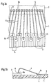
- FIGS 1a and 1b show a rack 1, the corresponds to the previously known prior art.
- a Subracks can e.g. a circuit board or a Be hybrid.
- Component 2 is on the subrack glued on or fastened in any other way.
- On the of the The main surface facing away from the top of the IC is numerous connections 5, only a few of which are shown in FIG. 1a are.
- the connectors are tight on the IC Grid arranged at a distance a of only 80 ⁇ m.
- the bonding tool is closed a pad 4 out, the wire from the capillary is pulled out.
- the wire forms a Loop shape.
- the capillary is now completely on the connection surface lowered and the wire under pressure, heat and ultrasound (Thermosonic welding) with the connection surface 4 welded.
- the capillary rim forms wedge-shaped welding tool with which the end 6b of the bonding wire squeezed on the pad, crappy and at the same time is separated from the wire in the capillary.
- the bonding tool needs one certain space on the pad so that the pads cannot be designed arbitrarily small.
- the pads 4 are integrated in the conductor tracks 3, so that now a connection 5 of the component 2 with a conductor track 3 is electrically connected via the bonding wire 6.
- the grid of the Connection surfaces 4 with the conductor tracks 3 are made much wider than the grid of the component connections (Distance dimension a).
- FIGS. 2a and 2b A rack 1 is shown in FIGS. 2a and 2b which was produced by the method according to the invention.
- the figures are only intended to show the essential content of the invention make it clear and are therefore what the magnitudes and e.g. the length of the bond wires is greatly simplified.
- the printed conductor pattern shown forms as in the case of FIG. 1a known solution shown a grid with each other parallel conductor track ends. The conductor ends 3 but can be much closer to that in comparison to Fig. 1a Component 2 be introduced.
- each component connection 5 is connected via two bonding wires 6 and 7 connected to a conductor track 3.
- the procedure is as follows that the first end designed in the form of a ball 6a of a bonding wire 6 with a connection 5 of the component 2 is shit.
- the pad 4 is not integrated in a conductor track 3, is located spatially separate from the Conductor tracks 3 on the area between the component 2 and the grid of the conductor tracks.
- the end 6b of the bonding wire 6a now the bondhead moved to a conductor track 3, which with this Pad 4 is to be connected.
- the conductor tracks 3 are located in a narrow grid on the subrack at a distance b from each other, which is approximately the distance a corresponds to the component connections. This is possible because in the subrack 1 shown in FIG.
- the width a pad 4 equal to or larger than the sum of the width of the assigned conductor track and the two distances this conductor path to the directly adjacent one Conductors can be without the pads the Traces overlap. But there are also larger distances b conceivable.
- the spherical or ball-shaped end 7a of a second Bond wire 7 is now first welded to the conductor track 3. This is easily possible because of the manufacture this shit connection does not take up as much space on the conductor tracks is claimed as for the preparation of the second Welded joint 7b. The connection can also be very narrow conductor tracks are produced.
- connection surfaces are advantageous 4 in the example shown here in three rows between the component 2 and the grid of the conductor tracks 3 arranged. This way, the available space becomes optimal utilized.
Abstract
Um bei einem Verfahren zur Herstellung von Bonddrahtverbindungen zwischen den Anschlüssen eines auf einem Baugruppenträger angeordneten Bauelements und darauf angeordneten Leiterbahnen durch Ball-Wedge-Bonden, wobei erste Enden der Bonddrähte durch das Bondwerkzeug zunächst kugelförmig oder ballartig geformt und wobei zweite Enden der Bonddrähte mit dem Bondwerkzeug auf den Leiterbahnen zugeordneten Anschlußflächen breitgequetscht und festgeschweißt werden, das Raster der Leiterbahnen möglichst eng auslegen zu können, wird vorgesschlagen, die den Leiterbahnen zugeordneten Anschlußflächen zwischen dem Bauelement und den Leiterbahnen und räumlich getrennt von den Leiterbahnen anzuordnen und die Anschlußflächen mit wenigstens einem Teil der Bauelementanschlüsse über erste Bonddrähte und mit den Leiterbahnen über zweite Bonddrähte zu verbinden, wobei jeweils das erste Ende des ersten Bonddrahtes mit einem Bauelementanschluß und das erste Ende des zweiten Bonddrahtes mit einer Leiterbahn verbunden wird und das zweite Ende des ersten Bonddrahtes und das zweiten Ende des zweiten Bonddrahtes mit der dieser Leiterbahn zugeordneten Anschlußfläche verbunden wird. <IMAGE>In a method for producing bond wire connections between the connections of a component arranged on a subrack and conductor tracks arranged thereon by ball-wedge bonding, first ends of the bond wires initially being spherical or ball-shaped by the bond tool and second ends of the bond wires with the bond tool are squeezed and welded onto the interconnects assigned to the interconnects, so that the grid of the interconnects can be designed as narrowly as possible, it is proposed to arrange the interconnects assigned to the interconnects between the component and the interconnects and spatially separated from the interconnects and the interconnects with at least some of the component connections to connect via first bond wires and to the conductor tracks via second bond wires, the first end of the first bond wire each having a component connection and the first end of the second bond wire m it is connected to a conductor track and the second end of the first bond wire and the second end of the second bond wire are connected to the connection area assigned to this conductor track. <IMAGE>
Description
Die Erfindung betrifft ein Verfahren zur Herstellung von
Bonddrahtverbindungen mit den im Oberbegriff des Anspruchs 1
angegebenen Merkmalen.The invention relates to a method for producing
Bond wire connections with the in the preamble of
Derartige Verfahren werden eingesetzt, um die elektrischen Anschlüsse eines auf einem Baugruppenträger plazierten elektronischen Bauelements, zum Beispiel eines Halbleiter-Chips, mit dem Leiterbahnmuster des Baugruppenträgers elektrisch zu verbinden. Dabei werden die Anschlüsse des Chips über Bonddrähte im sogenannten Ball-Wedge-Bondverfahren mit Anschlußflächen (Bondlands), welche den Leiterbahnen zugeordneten sind, verbunden. Beim Ball-Wedge-Bonden wird der Draht in einer Kapillare des Bondkopfes geführt. Ein von der Kapillare abstehendes erstes Ende des Drahtes wird z.B. durch eine Funkenentladung geschmolzen und bildet bedingt durch die Oberflächenspannung des geschmolzenen Lotes eine Kugel (Ball). Beim sogenannten Thermosonicschweißen wird beim Absenken der Kapillare auf einen Bauelementanschluß unter Druck-, Wärme und Ultraschalleinwirkung eine Schweißverbindung zwischen dem Bauelementanschluß und dem ersten Ende des Drahtes hergestellt. Anschließend wird die Kapillare zur Anschlußfläche (Bondland) einer Leiterbahn geführt, wobei der Draht aus der Kapillare herausgezogen wird. Beim Absenken der Kapillare wird das zweite Ende des Bonddrahtes durch den Kapillarenrand (Wedge) auf dem Bondland breitgequetscht und ebenfalls unter Druck-, Wärme und Ultraschalleinwirktung verschweißt und gleichzeitig von dem in der Kapillare geführten Draht abgetrennt. Nachteilig bei diesem Stand der Technik ist, daß die Herstellung der zweiten Schweißverbindung durch das Breitquetschen des Drahtes auf den Anschlußflächen sehr viel mehr Platz beansprucht als die Herstellung der Schweißverbindung zwischen den als Kugel ausgebildeten ersten Enden der Bonddrähte und den Bauelementanschlüssen. Der Abstand zwischen benachbarten Bauelementanschlüssen kann z.B. auf dem Chip bloß 80 µm betragen, während die Breite der Anschlußflächen (Bondlands) auf dem Baugruppenträger um ein vielfaches größer gewählt werden muß, damit das Bondwerkzeug auf die Anschlußfläche abgesenkt werden kann. Aus diesem Grund ist das Raster der den Leiterbahnen zugeordneten Anschlußflächen sehr viel größer als das Raster der Bauelementanschlüsse und beansprucht sehr viel mehr Platz auf dem Baugruppenträger. Weiterhin nachteilig ist, daß der Raum zwischen den Anschlußflächen der Leiterbahnen und dem Bauelement durch die Bonddrähte nur überspannt wird und deshalb ungenutzt bleibt.Such methods are used to control the electrical Connections of an electronic placed on a subrack Component, for example a semiconductor chip, with the conductor pattern of the subrack electrically connect. The connections of the chip are made using bond wires in the so-called ball-wedge bonding process with pads (Bondlands), which are assigned to the conductor tracks are connected. Ball-wedge bonding turns the wire in a capillary of the bondhead. One from the capillary protruding first end of the wire is e.g. by a Spark discharge melted and forms due to the Surface tension of the molten solder a ball (Ball). In so-called thermosonic welding, when lowering the capillary on a component connection Pressure, heat and ultrasound exposure to a welded joint between the component connector and the first end of the Wire. The capillary then becomes the connecting surface (Bondland) a conductor track, the Wire is pulled out of the capillary. When lowering the capillary becomes the second end of the bond wire through the Capillary rim (wedge) squeezed on the bondland and also under pressure, heat and ultrasound welded and at the same time from that guided in the capillary Wire cut off. A disadvantage of this state of the Technique is that of making the second welded joint by squeezing the wire onto the connection surfaces takes up a lot more space than manufacturing the welded connection between the balls first ends of the bond wires and the component connections. The distance between adjacent component connections can e.g. on the chip are just 80 µm while the width of the connection areas (Bondlands) on the subrack must be chosen many times larger so that the bonding tool can be lowered to the pad. Out for this reason, the grid is assigned to the conductor tracks Connection areas much larger than the grid of the component connections and takes up a lot more space the rack. Another disadvantage is that the room between the connection surfaces of the conductor tracks and the component is only spanned by the bond wires and therefore remains unused.
Das erfindungsgemäße Verfahren mit dem Kennzeichen des Anspruchs
1 hat demgegenüber den Vorteil, daß die für die Herstellung
der elektrischen Verbindung zwischen den Anschlüssen
eines Bauelements und den Leiterbahnen beim Ball-Wedge-Bonden
benötigte Verdrahtungsfläche auf dem Baugruppenträger
erheblich reduziert werden kann, indem die Anschlußflächen
für die zweiten Enden der Bonddrähte räumlich getrennt von
den Leiterbahnen zwischen dem Raster der Leiterbahnen und
dem Bauelement angeordnet werden und erst über zweite Bonddrähte
mit den Leiterbahnen verbunden werden. Vorteilhaft
können nun die in Kugelform (Ball) ausgebildeten ersten Enden
der Bonddrähte sowohl mit den Bauelementanschlüssen als
auch mit den Leiterbahnen verbunden werden. Da das Bondwerkzeug
hierfür nicht viel Platz benötigt, kann das Abstandsraster
der Leiterbahnen ebenso eng ausgelegt werden, wie das
Raster der Bauelementanschlüsse, also z.B. im 80 µm Raster.
Gleichzeitig können die Leiterbahnen enger an das Bauelement
herangeführt werden und die Bonddrahtlängen verkürzt werden.
Die zweiten Enden des jeweils ersten und zweiten Bonddrahtes
werden mit einer Anschlußfläche verschweißt, welche sich getrennt
von den Leiterbahnen und den Bauelementanschlüssen
auf dem Baugruppenträger befindet. Auf diese Weise wird auch
der Raum zwischen dem Bauelement und dem Leiterbahnraster
vorteilhaft genutzt.The method according to the invention with the characterizing part of the
Weiterhin ist vorteilhaft, daß mit dem erfindungsgemäßen Verfahren aufgrund der kurzen Bondwege weniger Drahtmaterial benötigt wird, was beim Golddrahtbonden die Herstellungskosten erheblich reduziert. Darüber hinaus werden die zur Herstellung von Bonddrähten ungenutzten Verfahrwege des Bondkopfes deutlich reduziert. Da bei dem erfindungsgemäßen Verfahren statt eines Bonddrahtes zwei verwandt werden, um die Verbindung von den Leiterbahnen zum Bauelement herzustellen, ist die Drahtführung der Bonddrähte insgesamt flacher, wodurch die mechanische Stabilität der Bondverbindungen erhöht wird.It is also advantageous that with the invention Processes less wire material due to the short bond paths what is required in gold wire bonding is the manufacturing cost significantly reduced. They are also used for manufacturing unused travels of the bond wire significantly reduced. Since in the method according to the invention instead of one bond wire two are used to make the Establish connection from the conductor tracks to the component, the wire routing of the bond wires is flatter overall, whereby increases the mechanical stability of the bond connections becomes.
Weitere vorteilhafte Ausgestaltungen werden durch die in den Unteransprüchen beschriebenen Merkmale ermöglicht. Falls der Platzbedarf für das Leiterbahnraster auf dem Baugruppenträger nicht unbedingt so klein wie möglich ausgelegt werden muß und statt dessen die Verfahrwege des Bondwerkzeugs möglichst klein gewählt werden sollen, ist es vorteilhaft, wenn nur jeder übernächste Bauelementanschluß über zwei Bonddrähte mit einer zugeordneten Leiterbahn verbunden wird und die übrigen Bauelementanschlüsse mit einer Anschlußfläche verbunden werden, die unmittelbar an die zugeordnete Leiterbahn angebunden ist.Further advantageous embodiments are in the Characteristics described sub-claims enables. If the Space required for the conductor track grid on the subrack are not necessarily designed to be as small as possible must and instead the travel paths of the bonding tool as possible should be chosen small, it is advantageous if only every next but one component connection via two bond wires is connected to an associated conductor track and the remaining component connections connected to a pad be directly connected to the assigned trace is connected.
Vorteilhaft kann die Breite einer Anschlußfläche größer ausgebildet werden als die Summe aus der Breite der zugeordneten Leiterbahn und den Abständen dieser Leiterbahn zu den auf dem Baugruppenträger direkt benachbarten Leiterbahnen.The width of a pad can advantageously be made larger are assigned as the sum of the width of the Trace and the distances of this trace to the on the subrack directly adjacent conductor tracks.
Besonders vorteilhaft ist es, die Anschlußflächen im Raum zwischen dem Bauelement und den Enden der Leiterbahnen in mehreren Reihen versetzt zueinander anzuordnen, da auf diese Weise der zur Verfügung stehende ungenutzte Raum zwischen dem Bauelement und dem Leiterbahnraster besonders effizient genutzt wird.It is particularly advantageous to connect the pads in the room between the component and the ends of the conductor tracks in several rows staggered to each other, because of this Way the available unused space between the component and the conductor track grid are particularly efficient is being used.
Ein Ausführungsbeispiel der Erfindung ist in der Zeichnung
dargestellt und wird in der nachfolgenden Beschreibung näher
erläutert. Es zeigt
Die Figuren 1a und 1b zeigen einen Baugruppenträger 1, der
dem bisher bekannten Stand der Technik entspricht. Ein solcher
Baugruppenträger kann z.B. eine Leiterplatte oder ein
Hybrid sein. Auf einer Hauptoberfläche des Baugruppenträgers
befindet sich wenigstens ein Bauelement 2, das z.B. ein IC
sein kann. Das Bauelement 2 ist auf den Baugruppenträger
aufgeklebt oder in sonstiger Weise befestigt. An der von der
Hauptoberfläche abgewandten Oberseite des IC's befinden sich
zahlreiche Anschlüsse 5, von denen nur einige in Fig. 1a gezeigt
sind. Die Anschlüsse sind auf dem IC mit einem engen
Raster in einem Abstand a von nur 80 µm angeordnet. Weiterhin
befindet sich ein Raster von Leiterbahnen 3 auf dieser
Hauptoberfläche des Baugruppenträgers 1, an deren Enden Anschlußflächen
4 vorgesehen sind, die mit den Anschlüssen 5
des Bauelementes 2 über Bonddrähte im Ball-Wedge-Bondverfahren
verbunden werden. Bei der Herstellung der Bonddrahtverbindung
wird ein Bondwerkzeug benutzt, bei dem der Draht in
einer Kapillare geführt wird, deren Durchmesser an den Draht
angepaßt ist. Als Bonddraht wird meist Golddraht verwandt.
Das Ende 6a des Drahtes unterhalb der Kapillare wird z.B.
durch die Energie einer Funkenentladung geschmolzen, wobei
die Schmelze bedingt durch die Oberflächenspannung eine Kugel
(Ball) bildet. Beim Absenken der Kapillare auf den Bauelementanschluß
2 wird an dem Ende 6a des Bonddrahtes 6 eine
Schweißverbindung durch Druck-, Wärme- und Ultraschalleinwirkung
hergestellt. Anschließend wird das Bondwerkzeug zu
einer Anschlußfläche 4 geführt, wobei der Draht aus der Kapillare
herausgezogen wird. Beim erneuten Absenken der Kapillare
auf der Anschlußfläche 4 bildet der Draht eine
Schlaufenform. Die Kapillare wird nun ganz auf die Anschlußfläche
abgesenkt und der Draht unter Druck-, Wärme und Ultraschalleinwirkung
(Thermosonicschweißen) mit der Anschlußfläche
4 verschweißt. Dabei bildet der Kapillarenrand ein
keilförmiges Schweißwerkzeug mit dem das Ende 6b des Bonddrahtes
auf der Anschlußfläche breitgequetscht, verscheißt
und gleichzeitig vom Draht in der Kapillare abgetrennt wird.
Bei diesem Verfahrensschritt benötigt das Bondwerkzeug einen
gewissen Platz auf der Anschlußfläche, so daß die Anschlußflächen
nicht beliebig klein ausgelegt sein können. Die Anschlußflächen
4 sind in den Leiterbahnen 3 integriert, so
daß nun ein Anschluß 5 des Bauelementes 2 mit einer Leiterbahn
3 über den Bonddraht 6 elektrisch verbunden ist. Wie
besonders gut in Fig. 1a zu erkennen ist, muß das Raster der
Anschlußflächen 4 mit den Leiterbahnen 3 (Abstandsmaß b)
sehr viel breiter ausgeführt werden als das Raster der Bauelementanschlüsse
(Abstandsmaß a). Insbesondere ist es nicht
möglich die Breite der Anschlußflächen 4 größer auszugestalten
als die Summe aus der Breite der jeweils zugeordneten
Leiterbahn und den beiden Abständen dieser Leiterbahn zu den
auf dem Baugruppenträger direkt benachbarten Leiterbahnen.Figures 1a and 1b show a
In den Figuren 2a und 2b ist ein Baugruppenträger 1 gezeigt
der nach dem erfindungsgemäßen Verfahren hergestellt wurde.
Die Figuren sollen nur den wesentlichen Inhalt der Erfindung
deutlich machen und sind daher, was die Größenordnungen und
z.B. die Länge der Bonddrähte anbelangt stark vereinfacht.
Das dargestellte Leiterbahnmuster bildet wie bei der in Fig.
1a dargestellten bekannten Lösung ein Raster mit zueinander
parallel verlaufenden Leiterbahnenden. Die Leiterbahnenden 3
können aber im Vergleich zu Fig. 1a sehr viel dichter an das
Bauelement 2 herangeführt sein. In dem hier gezeigten Beispiel
wird jeder Bauelementanschluß 5 über zwei Bonddrähte 6
und 7 mit einer Leiterbahn 3 verbunden. Dabei wird so verfahren,
daß das in Kugelform (Ball) ausgestaltete erste Ende
6a eines Bonddrahtes 6 mit einem Anschluß 5 des Bauelementes
2 verscheißt wird. Anschließend wird das zweite Ende 6b des
Bonddrahtes 6 auf der Anschlußfläche 4 verschweißt. Die Anschlußfläche
4 ist aber nicht in eine Leiterbahn 3 integriert,
sonderen befindet sich räumlich getrennt von den
Leiterbahnen 3 auf dem Flächenstück zwischen dem Bauelement
2 und dem Raster der Leiterbahnen. Nach dem Breitquetschen
und Verschweißen des Endes 6b des Bonddrahtes 6a wird nun
der Bondkopf zu einer Leiterbahn 3 gefahren, die mit dieser
Anschlußfläche 4 verbunden werden soll. Die Leiterbahnen 3
befinden sich in einem engen Raster auf dem Baugruppenträger
in einem Abstand b voneinander, welcher etwa dem Abstand a
der Bauelementanschlüsse entspricht. Dies ist möglich, da
bei dem in Fig. 2a gezeigten Baugruppenträger 1 die Breite
einer Anschlußfläche 4 gleich oder größer als die Summe aus
der Breite der zugeordneten Leiterbahn und den beiden Abständen
dieser Leiterbahn zu den jeweils direkt benachbarten
Leiterbahnen sein kann, ohne daß die Anschlußflächen die
Leiterbahnen überlappen. Es sind aber auch größere Abstände
b denkbar. Das Kugel- oder Ballförmige Ende 7a eines zweiten
Bonddrahtes 7 wird nun zunächst mit der Leiterbahn 3 verschweißt.
Dies ist leicht möglich, da für die Herstellung
dieser Scheißverbindung nicht so viel Platz auf den Leiterbahnen
beansprucht wird, wie für die Herstellung der zweiten
Schweißverbindung 7b. Die Verbindung kann also auch auf sehr
schmalen Leiterbahnen hergestellt werden. Anschließend wird
das Bondwerkzeug zu der Anschlußfläche 4 zurückgeführt und
es wird das zweite Ende 7b des Bonddrahtes 7 mit der Anschlußfläche
4 verschweißt, wobei dieses Ende nun erneut
durch das Bondwerkzeug auf der Anschlußfläche 4 breitgedrückt
werden kann (Wedge-Bonden). Die übrigen Anschlüsse 5
werden in gleicher Weise mit den Leiterbahnen 3 verbunden,
so daß jeder Leiterbahn 3 über eine zugeordnete Anschlußfläche
4 mit einem Bauelementanschluß 5 über zwei Bonddrähte
6,7 verbunden ist. Die Bonddrähte 6 und 7 können dabei auch
so geführt sein, daß sie über die Anschlußflächen benachbarter
Bondrähte hinweggeführt sind. Vorteilhaft sind die Anschlußflächen
4 in dem hiergezeigten Beispiel in drei Reihen
zwischen dem Bauelement 2 und dem Raster der Leiterbahnen 3
angeordnet. So wird der zur Verfügung stehende Platz optimal
genutzt. A
Abweichend zu dem hier gezeigten Ausführungsbeispiel ist es
auch möglich, nur jeden übernächsten Bauelementanschluß 5
über zwei Bonddrähte mit einer Leiterbahn zu verbinden und
die übrigen Bonddrähte, wie im Stand der Technik bekannt,
mit nur einem Bonddraht mit einer Anschlußfläche zu verschweißen,
die unmittelbar in eine Leiterbahn integriert
ist. Bei diesem Verfahren sind die ungenutzten Verfahrwege
des Bondwerkzeuges noch geringer, obwohl nun das Raster der
Leiterbahnen 3 nicht ganz so eng gewählt werden kann, wie in
dem ersten Ausführungsbeispiel.It differs from the exemplary embodiment shown here
also possible, only every next but one
Claims (5)
Applications Claiming Priority (2)
| Application Number | Priority Date | Filing Date | Title |
|---|---|---|---|
| DE1997103639 DE19703639A1 (en) | 1997-01-31 | 1997-01-31 | Component connection method for electronic assembly group |
| DE19703639 | 1997-01-31 |
Publications (3)
| Publication Number | Publication Date |
|---|---|
| EP0867932A2 true EP0867932A2 (en) | 1998-09-30 |
| EP0867932A3 EP0867932A3 (en) | 2000-05-17 |
| EP0867932B1 EP0867932B1 (en) | 2008-10-15 |
Family
ID=7818941
Family Applications (1)
| Application Number | Title | Priority Date | Filing Date |
|---|---|---|---|
| EP19970119991 Expired - Lifetime EP0867932B1 (en) | 1997-01-31 | 1997-11-14 | Method for making wire connections |
Country Status (4)
| Country | Link |
|---|---|
| US (1) | US6232561B1 (en) |
| EP (1) | EP0867932B1 (en) |
| JP (1) | JPH10223673A (en) |
| DE (2) | DE19703639A1 (en) |
Families Citing this family (14)
| Publication number | Priority date | Publication date | Assignee | Title |
|---|---|---|---|---|
| US6657225B1 (en) * | 1998-03-25 | 2003-12-02 | Seiko Epson Corporation | Semiconductor component, active matrix substrate for a liquid crystal display, and methods of manufacturing such component and substrate |
| JP2001015541A (en) * | 1999-06-28 | 2001-01-19 | Sumitomo Electric Ind Ltd | Semiconductor device and its manufacture |
| KR20010080450A (en) * | 1999-09-16 | 2001-08-22 | 롤페스 요하네스 게라투스 알베르투스 | Use of additional bonding finger rows to improve wire bond density |
| KR20010064907A (en) * | 1999-12-20 | 2001-07-11 | 마이클 디. 오브라이언 | wire bonding method and semiconductor package using it |
| US6429515B1 (en) * | 2000-05-05 | 2002-08-06 | Amkor Technology, Inc. | Long wire IC package |
| KR100400032B1 (en) * | 2001-02-07 | 2003-09-29 | 삼성전자주식회사 | Semiconductor package having a changed substrate design using special wire bonding |
| CN100401488C (en) * | 2001-03-23 | 2008-07-09 | Nxp股份有限公司 | Chip module with bond-wire connections with small loop height |
| US6908843B2 (en) * | 2001-12-28 | 2005-06-21 | Texas Instruments Incorporated | Method and system of wire bonding using interposer pads |
| DE102009029040A1 (en) | 2009-08-31 | 2011-03-03 | Robert Bosch Gmbh | Apparatus and method for manufacturing a device |
| US8138595B2 (en) * | 2010-03-26 | 2012-03-20 | Stats Chippac Ltd. | Integrated circuit packaging system with an intermediate pad and method of manufacture thereof |
| US8203201B2 (en) * | 2010-03-26 | 2012-06-19 | Stats Chippac Ltd. | Integrated circuit packaging system with leads and method of manufacture thereof |
| CN102762040A (en) * | 2012-07-20 | 2012-10-31 | 杭州华三通信技术有限公司 | Method for forming golden fingers on PCB (printed circuit board) and processing method of PCB |
| KR20160095731A (en) * | 2015-02-04 | 2016-08-12 | 에스케이하이닉스 주식회사 | Package on package type stack package and method of manufacturing the same |
| DE102015207327A1 (en) | 2015-04-22 | 2016-10-27 | Robert Bosch Gmbh | Circuit arrangement for an electronic circuit |
Citations (2)
| Publication number | Priority date | Publication date | Assignee | Title |
|---|---|---|---|---|
| DE3447345A1 (en) * | 1983-12-27 | 1985-07-11 | Mitsubishi Denki K.K., Tokio/Tokyo | Integrated semiconductor circuit arrangement |
| US5365409A (en) * | 1993-02-20 | 1994-11-15 | Vlsi Technology, Inc. | Integrated circuit package design having an intermediate die-attach substrate bonded to a leadframe |
Family Cites Families (9)
| Publication number | Priority date | Publication date | Assignee | Title |
|---|---|---|---|---|
| JPS5546578A (en) * | 1978-09-30 | 1980-04-01 | Toshiba Corp | Method of mounting integrated circuit |
| JPS56100436A (en) * | 1980-01-17 | 1981-08-12 | Toshiba Corp | Manufacture of semiconductor element |
| US4415115A (en) * | 1981-06-08 | 1983-11-15 | Motorola, Inc. | Bonding means and method |
| JPS58210650A (en) * | 1982-06-01 | 1983-12-07 | Fujitsu Ltd | Semiconductor device |
| JPH02201948A (en) * | 1989-01-30 | 1990-08-10 | Toshiba Corp | Package of semiconductor device |
| JPH03167872A (en) * | 1989-11-28 | 1991-07-19 | Seiko Epson Corp | Lead frame semiconductor device |
| JPH04280462A (en) * | 1991-03-08 | 1992-10-06 | Mitsubishi Electric Corp | Lead frame and semiconductor device using this lead frame |
| JPH05243306A (en) * | 1992-02-28 | 1993-09-21 | Nec Corp | Resin-sealed semiconductor device |
| US5497032A (en) * | 1993-03-17 | 1996-03-05 | Fujitsu Limited | Semiconductor device and lead frame therefore |
-
1997
- 1997-01-31 DE DE1997103639 patent/DE19703639A1/en not_active Withdrawn
- 1997-11-14 EP EP19970119991 patent/EP0867932B1/en not_active Expired - Lifetime
- 1997-11-14 DE DE59712974T patent/DE59712974D1/en not_active Expired - Lifetime
-
1998
- 1998-01-28 US US09/015,033 patent/US6232561B1/en not_active Expired - Fee Related
- 1998-01-29 JP JP1657998A patent/JPH10223673A/en active Pending
Patent Citations (2)
| Publication number | Priority date | Publication date | Assignee | Title |
|---|---|---|---|---|
| DE3447345A1 (en) * | 1983-12-27 | 1985-07-11 | Mitsubishi Denki K.K., Tokio/Tokyo | Integrated semiconductor circuit arrangement |
| US5365409A (en) * | 1993-02-20 | 1994-11-15 | Vlsi Technology, Inc. | Integrated circuit package design having an intermediate die-attach substrate bonded to a leadframe |
Non-Patent Citations (2)
| Title |
|---|
| PATENT ABSTRACTS OF JAPAN vol. 004, no. 079 (E-014), 7. Juni 1980 (1980-06-07) & JP 55 046578 A (TOSHIBA CORP), 1. April 1980 (1980-04-01) * |
| PATENT ABSTRACTS OF JAPAN vol. 005, no. 171 (E-080), 30. Oktober 1981 (1981-10-30) & JP 56 100436 A (TOSHIBA CORP), 12. August 1981 (1981-08-12) * |
Also Published As
| Publication number | Publication date |
|---|---|
| EP0867932B1 (en) | 2008-10-15 |
| EP0867932A3 (en) | 2000-05-17 |
| DE19703639A1 (en) | 1998-08-06 |
| US6232561B1 (en) | 2001-05-15 |
| JPH10223673A (en) | 1998-08-21 |
| DE59712974D1 (en) | 2008-11-27 |
Similar Documents
| Publication | Publication Date | Title |
|---|---|---|
| DE19744266B4 (en) | A wire bonding | |
| DE69535629T2 (en) | ASSEMBLY OF ELECTRONIC COMPONENTS ON A PCB | |
| DE19651122C2 (en) | Semiconductor component with a semiconductor chip and a circuit board | |
| EP0867932B1 (en) | Method for making wire connections | |
| DE10324598A1 (en) | Semiconductor device | |
| DE19747105A1 (en) | Component with stacked semiconductor chips | |
| DE102005011429A1 (en) | Wire bonding method and semiconductor device | |
| DE3913221A1 (en) | SEMICONDUCTOR ARRANGEMENT | |
| DE10295972T5 (en) | Non-molded package for a semiconductor device | |
| DE4207198A1 (en) | FEEDER FRAME AND SEMICONDUCTOR DEVICE USING THE FEEDER FRAME | |
| DE69628964T2 (en) | Resin molded semiconductor device and manufacturing process | |
| DE69737320T2 (en) | Semiconductor device | |
| DE69723801T2 (en) | Manufacturing process of a contact grid semiconductor package | |
| DE19651549B4 (en) | Connection frame and chip housing | |
| DE10153666B4 (en) | High density contact assembly and method of arranging contacts | |
| WO1996002042A1 (en) | Supporting component for use in chip cards or other data medium boards | |
| DE10205698A1 (en) | Light-emitting diode has electrical wirings formed on surface of insulated cup for electrical connection to LED chip stored in insulated cup | |
| DE102013018518A1 (en) | IC module for different connection techniques | |
| EP0995235B1 (en) | Contact for very small liaison contacts and method for producing a contact | |
| DE10212742A1 (en) | Wiring board contact pins soldering method for electronic device, involves irradiating laser light on solder balls on electrode pads to form fillets between pads and pedestals for soldering contact pins | |
| DE3614087A1 (en) | DEVICE AND METHOD FOR IMPROVED ENCLOSURE OF SEMICONDUCTOR DEVICES | |
| DE10139985B4 (en) | Electronic component with a semiconductor chip and method for its production | |
| DE3813566A1 (en) | Electrical connection between a hybrid assembly and a printed circuit board, and a method for its production | |
| WO2007014800A1 (en) | Chip module for installing in sensor chip cards for fluidic applications and method for producing a chip module of this type | |
| DE102020100364B4 (en) | Power electronic assembly with a substrate, a sleeve and a contact pin and method for producing such an assembly |
Legal Events
| Date | Code | Title | Description |
|---|---|---|---|
| PUAI | Public reference made under article 153(3) epc to a published international application that has entered the european phase |
Free format text: ORIGINAL CODE: 0009012 |
|
| AK | Designated contracting states |
Kind code of ref document: A2 Designated state(s): DE FR GB |
|
| AX | Request for extension of the european patent |
Free format text: AL;LT;LV;MK;RO;SI |
|
| PUAL | Search report despatched |
Free format text: ORIGINAL CODE: 0009013 |
|
| AK | Designated contracting states |
Kind code of ref document: A3 Designated state(s): AT BE CH DE DK ES FI FR GB GR IE IT LI LU MC NL PT SE |
|
| AX | Request for extension of the european patent |
Free format text: AL;LT;LV;MK;RO;SI |
|
| 17P | Request for examination filed |
Effective date: 20001117 |
|
| AKX | Designation fees paid |
Free format text: DE FR GB |
|
| R17C | First examination report despatched (corrected) |
Effective date: 20070426 |
|
| GRAP | Despatch of communication of intention to grant a patent |
Free format text: ORIGINAL CODE: EPIDOSNIGR1 |
|
| GRAS | Grant fee paid |
Free format text: ORIGINAL CODE: EPIDOSNIGR3 |
|
| GRAA | (expected) grant |
Free format text: ORIGINAL CODE: 0009210 |
|
| AK | Designated contracting states |
Kind code of ref document: B1 Designated state(s): DE FR GB |
|
| REG | Reference to a national code |
Ref country code: GB Ref legal event code: FG4D Free format text: NOT ENGLISH |
|
| REF | Corresponds to: |
Ref document number: 59712974 Country of ref document: DE Date of ref document: 20081127 Kind code of ref document: P |
|
| PLBE | No opposition filed within time limit |
Free format text: ORIGINAL CODE: 0009261 |
|
| STAA | Information on the status of an ep patent application or granted ep patent |
Free format text: STATUS: NO OPPOSITION FILED WITHIN TIME LIMIT |
|
| 26N | No opposition filed |
Effective date: 20090716 |
|
| PGFP | Annual fee paid to national office [announced via postgrant information from national office to epo] |
Ref country code: GB Payment date: 20091123 Year of fee payment: 13 Ref country code: FR Payment date: 20091202 Year of fee payment: 13 |
|
| PGFP | Annual fee paid to national office [announced via postgrant information from national office to epo] |
Ref country code: DE Payment date: 20110125 Year of fee payment: 14 |
|
| GBPC | Gb: european patent ceased through non-payment of renewal fee |
Effective date: 20101114 |
|
| REG | Reference to a national code |
Ref country code: FR Ref legal event code: ST Effective date: 20110801 |
|
| PG25 | Lapsed in a contracting state [announced via postgrant information from national office to epo] |
Ref country code: FR Free format text: LAPSE BECAUSE OF NON-PAYMENT OF DUE FEES Effective date: 20101130 |
|
| PG25 | Lapsed in a contracting state [announced via postgrant information from national office to epo] |
Ref country code: GB Free format text: LAPSE BECAUSE OF NON-PAYMENT OF DUE FEES Effective date: 20101114 |
|
| REG | Reference to a national code |
Ref country code: DE Ref legal event code: R119 Ref document number: 59712974 Country of ref document: DE Effective date: 20120601 |
|
| PG25 | Lapsed in a contracting state [announced via postgrant information from national office to epo] |
Ref country code: DE Free format text: LAPSE BECAUSE OF NON-PAYMENT OF DUE FEES Effective date: 20120601 |