EP0867293A2 - Process for joining a flexible circuit to a polymeric container and for forming a barrier layer over sections of the flexible circuit and other elements using an encapsulant material - Google Patents
Process for joining a flexible circuit to a polymeric container and for forming a barrier layer over sections of the flexible circuit and other elements using an encapsulant material Download PDFInfo
- Publication number
- EP0867293A2 EP0867293A2 EP98302341A EP98302341A EP0867293A2 EP 0867293 A2 EP0867293 A2 EP 0867293A2 EP 98302341 A EP98302341 A EP 98302341A EP 98302341 A EP98302341 A EP 98302341A EP 0867293 A2 EP0867293 A2 EP 0867293A2
- Authority
- EP
- European Patent Office
- Prior art keywords
- container
- outer portion
- print cartridge
- set forth
- ink jet
- Prior art date
- Legal status (The legal status is an assumption and is not a legal conclusion. Google has not performed a legal analysis and makes no representation as to the accuracy of the status listed.)
- Withdrawn
Links
- 239000000463 material Substances 0.000 title claims abstract description 74
- 239000008393 encapsulating agent Substances 0.000 title claims abstract description 46
- 230000004888 barrier function Effects 0.000 title claims abstract description 39
- 238000000034 method Methods 0.000 title claims abstract description 37
- 230000008569 process Effects 0.000 title claims abstract description 23
- 239000000853 adhesive Substances 0.000 claims abstract description 34
- 230000001070 adhesive effect Effects 0.000 claims abstract description 33
- 239000002318 adhesion promoter Substances 0.000 claims abstract description 19
- BLRPTPMANUNPDV-UHFFFAOYSA-N Silane Chemical compound [SiH4] BLRPTPMANUNPDV-UHFFFAOYSA-N 0.000 claims abstract description 14
- 229910000077 silane Inorganic materials 0.000 claims abstract description 13
- 238000007789 sealing Methods 0.000 claims abstract description 7
- 239000010410 layer Substances 0.000 claims description 41
- 239000000758 substrate Substances 0.000 claims description 34
- 239000011324 bead Substances 0.000 claims description 24
- 239000004020 conductor Substances 0.000 claims description 8
- 239000004820 Pressure-sensitive adhesive Substances 0.000 claims description 7
- 230000000694 effects Effects 0.000 claims description 6
- UHESRSKEBRADOO-UHFFFAOYSA-N ethyl carbamate;prop-2-enoic acid Chemical compound OC(=O)C=C.CCOC(N)=O UHESRSKEBRADOO-UHFFFAOYSA-N 0.000 claims description 5
- 239000012790 adhesive layer Substances 0.000 claims description 3
- 239000011440 grout Substances 0.000 claims description 2
- 239000011248 coating agent Substances 0.000 claims 3
- 238000000576 coating method Methods 0.000 claims 3
- NIXOWILDQLNWCW-UHFFFAOYSA-N acrylic acid group Chemical group C(C=C)(=O)O NIXOWILDQLNWCW-UHFFFAOYSA-N 0.000 claims 1
- 238000010438 heat treatment Methods 0.000 description 10
- 239000002313 adhesive film Substances 0.000 description 5
- 229920001187 thermosetting polymer Polymers 0.000 description 5
- 239000003522 acrylic cement Substances 0.000 description 4
- 229920000642 polymer Polymers 0.000 description 4
- LFQSCWFLJHTTHZ-UHFFFAOYSA-N Ethanol Chemical compound CCO LFQSCWFLJHTTHZ-UHFFFAOYSA-N 0.000 description 3
- 101100230510 Oryza sativa subsp. japonica HATB gene Proteins 0.000 description 3
- 239000000126 substance Substances 0.000 description 3
- 239000004721 Polyphenylene oxide Substances 0.000 description 2
- 230000008901 benefit Effects 0.000 description 2
- 239000008367 deionised water Substances 0.000 description 2
- 229910021641 deionized water Inorganic materials 0.000 description 2
- 239000007788 liquid Substances 0.000 description 2
- 229920006380 polyphenylene oxide Polymers 0.000 description 2
- XLYOFNOQVPJJNP-UHFFFAOYSA-N water Chemical compound O XLYOFNOQVPJJNP-UHFFFAOYSA-N 0.000 description 2
- RYGMFSIKBFXOCR-UHFFFAOYSA-N Copper Chemical compound [Cu] RYGMFSIKBFXOCR-UHFFFAOYSA-N 0.000 description 1
- 239000004593 Epoxy Substances 0.000 description 1
- 239000004727 Noryl Substances 0.000 description 1
- 229920001207 Noryl Polymers 0.000 description 1
- 239000004642 Polyimide Substances 0.000 description 1
- XAGFODPZIPBFFR-UHFFFAOYSA-N aluminium Chemical compound [Al] XAGFODPZIPBFFR-UHFFFAOYSA-N 0.000 description 1
- 229910052782 aluminium Inorganic materials 0.000 description 1
- 238000007796 conventional method Methods 0.000 description 1
- 229910052802 copper Inorganic materials 0.000 description 1
- 239000010949 copper Substances 0.000 description 1
- 230000007797 corrosion Effects 0.000 description 1
- 238000005260 corrosion Methods 0.000 description 1
- 229940075894 denatured ethanol Drugs 0.000 description 1
- 238000001035 drying Methods 0.000 description 1
- 229920006334 epoxy coating Polymers 0.000 description 1
- 230000009477 glass transition Effects 0.000 description 1
- PCHJSUWPFVWCPO-UHFFFAOYSA-N gold Chemical compound [Au] PCHJSUWPFVWCPO-UHFFFAOYSA-N 0.000 description 1
- 229910052737 gold Inorganic materials 0.000 description 1
- 239000010931 gold Substances 0.000 description 1
- 238000009434 installation Methods 0.000 description 1
- 238000012423 maintenance Methods 0.000 description 1
- 230000007246 mechanism Effects 0.000 description 1
- 239000000203 mixture Substances 0.000 description 1
- 229920003223 poly(pyromellitimide-1,4-diphenyl ether) Polymers 0.000 description 1
- 229920001721 polyimide Polymers 0.000 description 1
- 229920001296 polysiloxane Polymers 0.000 description 1
- 230000002028 premature Effects 0.000 description 1
- 230000001681 protective effect Effects 0.000 description 1
- 230000005855 radiation Effects 0.000 description 1
- 150000004756 silanes Chemical class 0.000 description 1
- 229920001169 thermoplastic Polymers 0.000 description 1
- 239000004416 thermosoftening plastic Substances 0.000 description 1
Images


Classifications
-
- B—PERFORMING OPERATIONS; TRANSPORTING
- B41—PRINTING; LINING MACHINES; TYPEWRITERS; STAMPS
- B41J—TYPEWRITERS; SELECTIVE PRINTING MECHANISMS, i.e. MECHANISMS PRINTING OTHERWISE THAN FROM A FORME; CORRECTION OF TYPOGRAPHICAL ERRORS
- B41J2/00—Typewriters or selective printing mechanisms characterised by the printing or marking process for which they are designed
- B41J2/005—Typewriters or selective printing mechanisms characterised by the printing or marking process for which they are designed characterised by bringing liquid or particles selectively into contact with a printing material
- B41J2/01—Ink jet
- B41J2/17—Ink jet characterised by ink handling
- B41J2/175—Ink supply systems ; Circuit parts therefor
- B41J2/17503—Ink cartridges
- B41J2/17526—Electrical contacts to the cartridge
-
- B—PERFORMING OPERATIONS; TRANSPORTING
- B41—PRINTING; LINING MACHINES; TYPEWRITERS; STAMPS
- B41J—TYPEWRITERS; SELECTIVE PRINTING MECHANISMS, i.e. MECHANISMS PRINTING OTHERWISE THAN FROM A FORME; CORRECTION OF TYPOGRAPHICAL ERRORS
- B41J2/00—Typewriters or selective printing mechanisms characterised by the printing or marking process for which they are designed
- B41J2/005—Typewriters or selective printing mechanisms characterised by the printing or marking process for which they are designed characterised by bringing liquid or particles selectively into contact with a printing material
- B41J2/01—Ink jet
- B41J2/135—Nozzles
- B41J2/14—Structure thereof only for on-demand ink jet heads
- B41J2/14016—Structure of bubble jet print heads
- B41J2/14072—Electrical connections, e.g. details on electrodes, connecting the chip to the outside...
-
- B—PERFORMING OPERATIONS; TRANSPORTING
- B41—PRINTING; LINING MACHINES; TYPEWRITERS; STAMPS
- B41J—TYPEWRITERS; SELECTIVE PRINTING MECHANISMS, i.e. MECHANISMS PRINTING OTHERWISE THAN FROM A FORME; CORRECTION OF TYPOGRAPHICAL ERRORS
- B41J2/00—Typewriters or selective printing mechanisms characterised by the printing or marking process for which they are designed
- B41J2/005—Typewriters or selective printing mechanisms characterised by the printing or marking process for which they are designed characterised by bringing liquid or particles selectively into contact with a printing material
- B41J2/01—Ink jet
- B41J2/135—Nozzles
- B41J2/16—Production of nozzles
- B41J2/1601—Production of bubble jet print heads
-
- B—PERFORMING OPERATIONS; TRANSPORTING
- B41—PRINTING; LINING MACHINES; TYPEWRITERS; STAMPS
- B41J—TYPEWRITERS; SELECTIVE PRINTING MECHANISMS, i.e. MECHANISMS PRINTING OTHERWISE THAN FROM A FORME; CORRECTION OF TYPOGRAPHICAL ERRORS
- B41J2/00—Typewriters or selective printing mechanisms characterised by the printing or marking process for which they are designed
- B41J2/005—Typewriters or selective printing mechanisms characterised by the printing or marking process for which they are designed characterised by bringing liquid or particles selectively into contact with a printing material
- B41J2/01—Ink jet
- B41J2/135—Nozzles
- B41J2/16—Production of nozzles
- B41J2/1621—Manufacturing processes
- B41J2/1623—Manufacturing processes bonding and adhesion
-
- B—PERFORMING OPERATIONS; TRANSPORTING
- B41—PRINTING; LINING MACHINES; TYPEWRITERS; STAMPS
- B41J—TYPEWRITERS; SELECTIVE PRINTING MECHANISMS, i.e. MECHANISMS PRINTING OTHERWISE THAN FROM A FORME; CORRECTION OF TYPOGRAPHICAL ERRORS
- B41J2/00—Typewriters or selective printing mechanisms characterised by the printing or marking process for which they are designed
- B41J2/005—Typewriters or selective printing mechanisms characterised by the printing or marking process for which they are designed characterised by bringing liquid or particles selectively into contact with a printing material
- B41J2/01—Ink jet
- B41J2/135—Nozzles
- B41J2/14—Structure thereof only for on-demand ink jet heads
- B41J2002/14362—Assembling elements of heads
-
- H—ELECTRICITY
- H05—ELECTRIC TECHNIQUES NOT OTHERWISE PROVIDED FOR
- H05K—PRINTED CIRCUITS; CASINGS OR CONSTRUCTIONAL DETAILS OF ELECTRIC APPARATUS; MANUFACTURE OF ASSEMBLAGES OF ELECTRICAL COMPONENTS
- H05K3/00—Apparatus or processes for manufacturing printed circuits
- H05K3/36—Assembling printed circuits with other printed circuits
- H05K3/361—Assembling flexible printed circuits with other printed circuits
Definitions
- This invention relates to a process for joining a flexible circuit to an ink jet print cartridge container and to a process for forming a barrier layer over one or more extending sections of a flexible circuit and one or more bond pads of a printhead using an encapsulant material.
- Drop-on-demand ink jet printers use thermal energy to produce a vapor bubble in an ink-filled chamber to expel a droplet.
- a thermal energy generator or heating element usually a resistor, is located in the chamber on a heater chip near a discharge orifice.
- a plurality of chambers, each provided with a single heating element, are provided in the printer's printhead.
- the printhead typically comprises the heater chip and a plate having a plurality of the discharge orifices formed therein.
- the printhead forms part of an ink jet print cartridge which also comprises an ink-filled container.
- a flexible circuit is used to provide a path for energy pulses to travel from a printer energy supply circuit to the printhead.
- the flexible circuit includes a substrate portion and a plurality of traces located on the substrate portion.
- the traces have end sections which extend out from the substrate portion.
- the extending sections are coupled to bond pads on the printhead. Typically, there is a first row of coupled bond pads and trace sections and an opposing, second row of coupled bond pads and trace sections.
- barrier layer it is known in the art to form a barrier layer over each row of coupled bond pads and extending trace sections.
- One known process for forming such a barrier layer involves dispensing an encapsulant material onto the coupled bond pads and trace sections using a discharge needle having a circular cross section.
- a discharge needle having a circular cross section.
- two complete passes of the needle are made over each row of coupled bond pads and trace sections.
- the final height of the barrier layer relative to the flexible circuit is undesirably high, e.g., normally greater than .007 inch (0.18mm).
- a paper substrate which receives the ejected ink droplets, is spaced an increased distance from the printhead orifice plate. Consequently, misdirected ink droplets reach the paper substrate at locations which are spaced a greater distance from their intended contact points than if the paper substrate were located closer to the printhead orifice plate.
- the excessive height of the two barrier layers is further problematic as it makes it more difficult to apply a length of sealing tape to the printhead so as to seal the printhead orifices from ink leakage until the print cartridge is installed for use in a printer.
- a dispensing needle having an oval discharge orifice is used to dispense a single bead of encapsulant material, e.g., a polymeric adhesive material, over a row of coupled bond pads and extending trace sections.
- encapsulant material e.g., a polymeric adhesive material
- the bead height is reduced due to the oval cross section of the dispensing needle.
- the paper substrate which receives the ejected ink droplets, may be moved closer to the printhead, so as to improve print quality.
- sealing tape may be applied more easily and effectively to the printhead.
- the encapsulant material comprises an ultraviolet curable thermoset
- improved curing depth is achieved with the lower bead height.
- Such lower bead heights ensure proper capping at the maintenance station to prevent ink leakage.
- an adhesion promoter such as a silane solution, is applied to a portion of a print cartridge container before a flexible circuit is adhesively coupled to the container.
- the adhesion promoter improves adhesion at the adhesive-container interface.
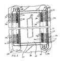
- FIG. 1 there is shown an ink jet print cartridge 10 constructed in accordance with the present invention. It is adapted to be used in an ink jet printer (not shown).
- the print cartridge 10 comprises an ink-filled polymeric container 12, a printhead 20 which is adhesively secured to the container 12, and a flexible circuit 30 (also referred to as a TAB circuit).
- the printhead 20 comprises a heater chip 22 provided with a plurality of resistive heating elements 24, see Fig. lA.
- the printhead 20 further includes an orifice plate 26 having a plurality of openings 28 extending through it which define a plurality of orifices 28a through which ink droplets are ejected. Sections 26a of the plate 26 and portions 22a of the heater chip 22 define a plurality of bubble chambers 29. Ink supplied by the container 12 flows into the bubble chambers 29 through ink supply channels 29a.
- the resistive heating elements 24 are individually addressed by voltage pulses. Each voltage pulse is applied to a heating element 24 to momentarily vaporize the ink in contact with the heating element 24 to form a bubble within the chamber 29 in which the heating element 24 is located. The function of the bubble is to displace ink within the chamber 29 such that a droplet of ink is expelled through the bubble chamber orifice 28a.
- the flexible circuit 30 provides a path for voltage pulses to travel from a printer energy supply circuit (not shown) to bond pads 20a, see Fig. 2, provided on the printhead 20. Conductors 24a extend from the bond pads 20a to the heating elements 24, see Fig. lA.
- the flexible circuit 30 comprises a substrate portion 32 and a plurality of metallic traces 34 formed on a first side 32a of the substrate portion 32, see Figs. 2 and 6.
- the traces 34 have main body sections 34a and end sections 34b.
- the main body sections 34a are formed on the substrate portion 32 and the end sections 34b extend out from the substrate portion 32.
- the end sections 34b define first and second rows of beam leads 34c and 34d.
- the first side 32a of the substrate portion 32 faces the container 12 such that the main body sections 34a are positioned between the substrate portion 32 and the container 12.
- An epoxy coating (not shown) may be applied over the main body sections 34a so as to prevent ink from contacting those sections 34a.
- the extending end sections 34b are coupled to the bond pads 20a via a conventional Tape Automated Bonding (TAB) bonding process.
- TAB bonding process is performed before either the printhead 20 or the flexible circuit 30 is secured to the container 12.
- the first and second rows 35a and 35b of coupled bond pads 20a and trace sections 34b are also referred to herein as first and second outer portions of the print cartridge 10.
- the polymeric container 12 may be formed from polyphenylene oxide, which is commercially available from the General Electric Company under the trademark "NORYL SE-1".
- the substrate portion 32 is preferably formed from a polymeric material, such as a polyimide material commercially available from E.I. DuPont de Nemours & Co. under the trademark "KAPTON.”
- the metallic traces 34 are gold-coated copper traces.
- the specific materials from which the container 12, the substrate portion 32 and metallic traces 34 are formed are mentioned herein for illustrative purposes only. Hence, in this invention, the materials from which these elements are formed are not intended to be limited to the specific ones disclosed herein.
- a die-attach adhesive (not shown), a heat curable epoxy-based polymer in the illustrated embodiment, is applied to a printhead receiving portion 13 of the container 12, see Fig. 7.
- An example of such an adhesive is one which is a commercially available polymeric material such as epoxy-type or silicone based adhesive.
- the adhesive is placed on the container and cured via conventional methods.
- a free-standing pressure sensitive adhesive film is used to secure the flexible circuit 30 to the container 12.
- Three separate sections 40a-40c of the pressure sensitive adhesive film are applied to three portions 12a-12c of the container 12 which receive the circuit 30, see Fig. 7.
- the film sections 40a-40c are preferably applied to the container portions 1 2a-1 2c before the die-attach adhesive is applied to the printhead receiving portion 13.
- Example pressure sensitive adhesive films include: 1) a .002 inch (0.05mm) thick acrylic adhesive film commercially available from 3M Corporation under the product designation "9460”; 2) a .005 inch (0.13mm) thick acrylic adhesive film commercially available from 3M Corporation under the product designation "9885”; 3) a .002 inch (0.05mm) thick acrylic adhesive film commercially available from Ashland Chemical Company, Specialty Polymers and Adhesives Division under the trademark "AEROSET 1 860Z-45”; and 4) a .002 inch (0.05mm) thick acrylic adhesive film commercially available from Ashland Chemical Company, Specialty Polymers and Adhesives Division under the trademark "AEROSET 1930-Z47".
- an adhesion promoter 50 may be applied directly to the first, second and third container portions 12a-12c before they receive the adhesive film sections 40a-40c.
- the flexible circuit 30 with the printhead 20 bonded to it is attached to the container 12 with pressure being applied.
- the container 12, after receiving the film sections 40a-40c, the flexible circuit 30 and the printhead 20, is heated to a temperature of about greater than ambient to about less than the glass transition temperature of the container 12, and preferably, from about 100°C to about 120°C for at least about 30 minutes and preferably for about 45 minutes to effect the curing of the die-attach adhesive.
- adhesion promoter 50 When an adhesion promoter 50 is not used, premature adhesion failure may occur at the container-adhesive interface as a result of this heating step.
- Use of the adhesion promoter 50 improves adhesion at the adhesive-container interface after the container 12, with the adhesive film sections 40a-40c secured thereto, has been heated to effect the curing of the die-attach adhesive.
- the adhesion promoter 50 is preferably prepared as a solution comprising about 0.1 to about 1.0% by volume of silane; greater than about 98% by volume of denatured ethanol; and 0.2 to about 0.4% by volume of deionized water.
- the silane may comprise either of two silanes which are commercially available from Dow Corning Corporation under the product designations "Z6030" and "Z6032". The three components are mixed at ambient temperature and allowed to stabilize.
- the solution may be applied to the container portions 12a-12c about one hour after mixing. The solution is stable for about one week if kept at ambient conditions.
- the adhesion promoter solution is preferably applied manually using a commercially available grout sealer pen (not shown) from Color Tile under Stock No. 7893217. Alternatively, other applicators such as brushes and the like may be used.
- the three pressure sensitive adhesive sections 40a-40c are secured under pressure to the container portions 12a-12c.
- the adhesive sections 40a-40c preferably have release liners (not shown) covering their outer surfaces, which surfaces will engage the flexible circuit 30. The release liners are removed just before the flexible circuit 30 is secured to the container 12.
- the coupled printhead 20 and flexible circuit 30 is secured to the container 12.
- the flexible circuit 30 is pressed against the sections 40a-40c under sufficient pressure to effect bonding between the sections 40a-40c and the circuit 30.
- the cartridge 10 is heated in an oven maintained at a temperature of about 110°C for approximately 45 minutes so as to effect the curing of the die-attach adhesive.
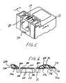
- a single bead of liquid encapsulant material 60 is applied over each of the two rows 35a and 35b of coupled bond pads 20a and extending trace sections 34b.
- the liquid encapsulant material is preferably dispensed through a dispensing needle 70 having an oval cross section, see Figs. 3 and 4.
- the dispensing needle 70 is attached to a conventional dispensing apparatus 72 having a dispense pump (not shown) which forces encapsulant material 60 from a tube of encapsulant material (not shown) into and through the dispensing needle 70.
- the apparatus 72 also has a traversing mechanism (not shown) which moves the needle 70 along dispensing paths so as to allow the needle 70 to deposit the material 60 along the two rows 35a and 35b.
- a workpiece holder 74 is provided to fixedly hold the container 12 beneath the dispensing needle 70. It is also contemplated that the material 60 may be manually dispensed through the needle 70 using a conventional syringe.
- the encapsulant material 60 forms a first barrier layer 60a over row 35a and a second barrier layer 60b over row 35b, see Fig. 2.
- the encapsulant material 60 may comprise any polymeric material which, after it has substantially solidified or cured, is capable of forming an effective mechanical and chemical protective barrier layer over each of the two rows 35a and 35b of coupled bond pads 20a and extending trace sections 34b.
- the bond pads 20a are made from aluminum in the illustrated embodiment.
- the barrier layers 60a and 60b protect the bond pads 20a from corrosion due to exposure to ink.
- the barrier layers 60a and 60a further protect the bond pads 20a and extending sections 34a from damage caused by a conventional polymeric wiper (not shown) which forms part of the printer and moves across the plate 26 so as to remove ink therefrom.
- the encapsulant material 60 may comprise a urethane acrylate material which is commercially available from Grace Specialty Polymers Division of W.R. Grace and Company under the trademark "UNISET UV-9000.” This material is an ultraviolet light (UV) cured material and has a viscosity of about 11,000 centipoise (11Pa.s) at about 25°C when measured with a Brookfield viscometer, Model HATB. Other thermoset or thermoplastic encapsulant materials not specifically set out herein may also be used.
- the needle 70 has an oval discharge orifice 70a, see Fig. 4, having a first dimension D 1 along a first axis A 1 and second dimension D 2 along a second axis A 2 .
- the second dimension D 2 is less than the first dimension D1.
- the second axis A 2 is substantially orthogonal to the first axis A 1 .
- a ratio of the first dimension D 1 to the second dimension D 2 is greater than or equal to about 1.1:1.0 and less than or equal to about 7.0:1.0, and most preferably is about 4.0:1.0.
- D 1 may be equal to about 2 mm and D 2 may be equal to about .5 mm.
- the printhead 20 is attached to the flexible circuit 30.
- the long or first axis A 1 of the oval discharge orifice 70a is orthogonal to the long axis of the encapsulant bead and the row 35a or 35b to which the encapsulant material 60 is applied.
- the height of the bead of encapsulant material dispensed onto each of the two rows 35a and 35b of coupled bond pads 20a and extending trace sections 34b is reduced over bead height achieved using a needle having a substantially circular cross section. If the encapsulant material is a UV curable thermoset, improved curing depth is achieved as a result of reduced bead height.
- the maximum height H b of the encapsulant material after it has solidified or cured, as measured from the upper portion 26b of plate 26 to the highest portion or point of the solidified or cured encapsulant bead is less than about .02 inch (0.5mm), see Fig. 6. More preferably, the maximum height H b is less than about .007 inch (0.18mm), and most preferably, is from about .004 inch (0.lmm) to about .006 inch (0.15mm). Because of reduced barrier layer height, a paper substrate, which receives the ejected ink droplets, may be moved closer to the printhead 20 so as to improve print quality. Further, sealing tape 80, see Fig.
- a polymeric cap (not shown) forming part of the printer is sealed over the printhead. If the height of the barrier layers 60a and 60b is too excessive and the polymeric cap is out of tolerances such that it engages one or both of the barrier layers 60a and 60b, adequate sealing may not be achieved. With lower barrier layer height, the likelihood of proper capping is increased.
- a further advantage resulting from the oval shape of the discharge orifice 70a is that only a single pass of the needle 70 is required over each of the two rows 35a and 35b of coupled bond pads 20a and extending trace sections 34b to form a barrier layer having an acceptable width. Accordingly, this process is more efficient than prior art processes which require two or more passes to form an acceptable barrier layer.
- the encapsulant material 60 may have a viscosity of between about 7,000 centipoise (7Pa.s) and about 60,000 centipoise (60Pa.s) at 25°C, as measured by a Brookfield viscometer, model HATB with appropriate spindle at 0.5 RPM.
- a higher viscosity encapsulant material 60 may be used. Generally, a higher viscosity material results in a higher bead height. However, with a higher viscosity material, less sag or drop of the encapsulant material between the extending trace sections 34b occurs. Hence, a more uniform barrier layer outer surface is formed.
- thermoset adhesive which is commercially available from W.R. Grace and Company under the trademark "Uniset 3032-78," having a viscosity of approximately 50,000 centipoise (50Pa.s) at 25°C, when measured using a Brookfield viscometer, Model HATB with spindle 52; and a thermoset adhesive which is commercially available from Ablestik Company under the trademark "Ablebond 84-3,” having a viscosity of approximately 50,000 centipoise (50Pa.s) at 25°C when measured using a Brookfield viscometer, Model HBT-DCP with spindle CP-51.
- the encapsulant material 60 is cured via exposure to ultraviolet radiation. Thereafter, the die-attach adhesive is cured by placing the cartridge 10 in a heated oven maintained at a temperature of about 110°C for approximately 45 minutes.
- An adhesion promoter solution was prepared by combining approximately 85 ml of ethanol; approximately .5 ml of silane (Z6032); and approximately 50 drops of deionized water. After the mixture was gently mixed and allowed to stabilize for one hour, the solution was applied to second and third portions 12b and 12c of a first ink jet print cartridge container formed from polyphenylene oxide. Two separate sections of adhesive film (commercially available from 3M Corporation under the product designation "9460") were applied to the second and third container portions. A first flexible circuit was then applied to the pressure sensitive adhesive sections. As a third section of adhesive film was not applied to the first container portion 12a, the flexible circuit was not folded down and secured to container portion 12a. A second container, which was not coated with the adhesion promoter solution, received two separate sections of the same adhesive film. A flexible circuit was then secured to the container via the two sections of pressure sensitive adhesive film.
- a die-attach adhesive was not applied to the first and second containers.
- Adhesion of each flexible circuit to its respective container was measured after heating using an Instron testing machine. Each container was placed in the testing machine. Movable grips, forming part of the machine, were secured to each container's unsecured section of the flexible circuit so as to apply a pulling force to the flexible circuit. The containers were held fixed in the testing machine. Approximately 300 grams of force were required to peel the flexible circuit from the first container while approximately 230 grams of force were required to peel the flexible circuit from the second container. Hence, peel strength improved by at least 30% when an adhesion promoter 50 was applied.
- the mode of failure for the first container was within the adhesive layer, not at the adhesive-container interface.
- the mode of failure for the second container was at the adhesive-container interface.
Abstract
Description
Claims (36)
- A method for sealing at least one outer portion of an ink jet print cartridge comprising the steps of:providing a dispensing element having an oval discharge orifice; anddispensing an encapsulant material onto said at least one outer portion via said dispensing element so as to provide a barrier layer over said at least one outer portion.
- A method as set forth in claim 1, wherein said ink jet print cartridge comprises:a polymeric container adapted to receive ink;a printhead coupled to said container and having at least one bond pad;a flexible circuit including a substrate portion and at least one conductor trace on said substrate portion and having an end section which extends out from said substrate portion to define at least one beam lead, said at least one beam lead being coupled to said at least one bond pad; andsaid outer portion of said ink jet print cartridge comprising said at least one bond pad and said at least one beam lead.
- A method as set forth in claim 1 or 2, wherein said dispensing step comprises the step of moving one of said dispensing element and said outer portion relative to the other such that only a single bead of encapsulant material is applied to said outer portion, said single bead of encapsulant material being sufficient to substantially completely cover said outer portion.
- A method as set forth in claim 1, 2 or 3, wherein said dispensing step comprises the step of dispensing a polymeric encapsulant material onto said outer portion such that after said polymeric material has substantially cured or solidified it has a height which is less than about .02 inch (0.5mm).
- A method as set forth in claim 4, wherein said dispensing step comprises the step of dispensing a polymeric encapsulant material onto said outer portion such that after said polymeric material has cured or solidified it has a height which is between about .004 inch (0.1mm) and about .006 inch (0.15mm).
- A method as set forth in any preceding claim, wherein said dispensing step comprises the step of dispensing a polymeric material onto said outer portion.
- A method as set forth in claim 6, wherein said polymeric material comprises a urethane acrylate material.
- A method as set forth in any preceding claim, wherein said dispensing step comprises the step of dispensing a polymeric material onto said outer portion having a viscosity between about 7,000 centipoise (7Pa.s) and about 60,000 centipoise (60Pa.s).
- A method as set forth in any preceding claim, wherein said ink jet print cartridge comprises:a polymeric container adapted to receive ink;a printhead coupled to said container and having a first row of bond pads located on a first side of said printhead and a second row of bond pads which are located on a second side of said printhead which is opposite to said first side;a flexible circuit including a substrate portion and a plurality of conductor traces provided on said substrate portion and having end sections which extend out from said substrate portion to define first and second rows of beam leads, said first row of beam leads being coupled to said first row of bond pads and said second row of beam leads being coupled to said second row of bond pads, said coupled first bond pads and beam leads defining a first print cartridge outer portion and said coupled second bond pads and beam leads defining a second print cartridge outer portion.
- A method as set forth in claim 9, wherein said dispensing step comprises the steps of:moving one of said dispensing element and said first outer portion relative to the other such that only a single bead of encapsulant material is applied over said first outer portion, said single bead of encapsulant material being sufficient to substantially completely cover said first outer portion; andmoving one of said dispensing element and said second outer portion relative to the other such that only a single bead of encapsulant material is applied onto said second outer portion, said single bead of encapsulant material being sufficient to substantially completely cover said second outer portion.
- A method as set forth in any preceding claim, wherein said oval discharge orifice has a first dimension along a first axis and second dimension along a second axis which is less than said first dimension, said second axis being substantially orthogonal to said first axis, and a ratio of said of first dimension to said second dimension is greater than or equal to about 1.1:1 and less than or equal to about 7:1.
- An ink jet print cartridge comprising:at least one outer portion; anda bead of encapsulant material provided over said at least one outer portion so as to provide a barrier layer over said outer portion, said barrier layer having a height which is less than about .007 inch (0.18mm).
- An ink jet print cartridge as set forth in claim 12, further comprising:a polymeric container adapted to receive ink;a printhead coupled to said container and having at least one bond pad; anda flexible circuit including a substrate portion and at least one conductor trace provided on said substrate portion and having an end section which extends out from said substrate portion to define at least one beam lead, said at least one beam lead being coupled to said at least one bond pad, and said coupled beam lead and bond pad defining said outer portion.
- An ink jet print cartridge as set forth in claim 12 or 13, wherein said barrier layer has a height which is between about .004 inch (0.lmm) and about .006 inch (0.15mm).
- An ink jet print cartridge as set forth in claim 12, 13 or 14, wherein said encapsulant material comprises a polymeric material.
- An ink jet print cartridge as set forth in claim 15, wherein said polymeric material comprises a urethane acrylate material.
- An ink jet print cartridge as set forth in any of claims 12 to 16, further comprising:a polymeric container adapted to receive ink;a printhead coupled to said container and having a first row of bond pads located on a first side of said printhead and a second row of bond pads which are located on a second side of said printhead which is opposite to said first side;a flexible circuit including a substrate portion and a plurality of conductor traces provided on said substrate portion and having end sections which extend out from said substrate portion to define first and second rows of beam leads, said first row of beam leads being coupled to said first row of bond pads and said second row of beam leads being coupled to said second row of bond pads, said coupled first beam leads and bond pads defining a first outer portion of said print cartridge and said coupled second beam leads and bond pads defining a second outer portion of said print cartridge; anda first bead of encapsulant material provided over said first outer portion and forming a barrier layer over said first outer portion and a second bead of encapsulant material provided over said second outer portion and forming a barrier layer over said second outer portion, said first and second barrier layers having a height which is less than about .02 inch (0.5mm).
- An ink jet print cartridge as set forth in claim 17, wherein said first and second barrier layers have a height which is between about .004 inch (0.lmm) and about .006 inch (0.15mm).
- A process for joining a flexible circuit to an ink jet print cartridge container comprising the steps of:coating a silane adhesion promoter to a portion of said container;applying an adhesive to at least a part of said silane-coated portion; andadhering said flexible circuit to said container via said adhesive.
- A process as set forth in claim 19, wherein said step of applying an adhesive comprises the step of applying an acrylic pressure-sensitive adhesive to said at least a part of said silane-coated portion.
- A process as set forth in claim 19 or 20, wherein said silane adhesion promoter is applied to said container with a grout sealer pen.
- An ink jet print cartridge comprising:a polymeric container adapted to receive ink;a printhead coupled to said container;a layer of silane coated on a portion of said container;a layer of adhesive provided on at least a part of said silane-coated portion; anda flexible circuit including a substrate portion adhered to said container via said adhesive layer.
- An ink jet print cartridge as set forth in claim 22, wherein said printhead has at least one bond pad and said flexible circuit has at least one conductor trace provided on said substrate portion, said conductor trace having an end section which extends out from said substrate portion to define at least one beam lead, said at least one beam lead being coupled to said at least one bond pad, and said coupled beam lead and bond pad defining an outer portion of said ink jet print cartridge.
- An ink jet print cartridge as set forth in claim 23, further including a bead of encapsulant material provided over said outer portion so as to form a barrier layer over said outer portion, said barrier layer having a height which is less than about .02 inch (0.5mm).
- An ink jet print cartridge as set forth in claim 22, 23 or 24, wherein said encapsulant material comprises a polymeric material.
- An ink jet print cartridge as set forth in claim 25, wherein said polymeric material comprises a urethane acrylate material.
- An ink jet print cartridge as set forth in claim 24, said barrier layer having a height which is between about .004 inch (0.lmm) and about .006 inch (0.15mm).
- An ink jet print cartridge comprising:a polymeric container adapted to receive ink;a printhead coupled to said container, said printhead having at least one bond pad;a layer of an adhesion promoter provided on a portion of said container;a layer of adhesive provided over at least a part of said adhesion promoter on said container portion;a flexible circuit adhered to said container via said adhesive layer, said flexible circuit including a substrate portion and at least one conductor trace provided on said substrate portion and having an end section which extends out from said substrate portion to define at least one beam lead, said at least one beam lead being coupled to said at least one bond pad, and said coupled beam lead and bond pad defining an outer portion of said ink jet print cartridge; anda bead of encapsulant material provided over said outer portion so as to form a barrier layer over said outer portion, said barrier layer having a height which is less than about .01 inch (0.25mm).
- An ink jet print cartridge as set forth in claim 28, wherein said barrier layer has a height which is between about .004 inch (0.lmm) and about .006 inch (0.15mm).
- An ink jet print cartridge as set forth in claim 28 or 29, wherein said encapsulant material comprises a polymeric material.
- An ink jet print cartridge as set forth in claim 30, wherein said polymeric material comprises a urethane acrylate material.
- A process for joining a flexible circuit and a printhead to an ink jet print cartridge container comprising the steps of:applying a die-attach adhesive to a first portion of said container;coating an adhesive promoter to at least one second portion of said container;securing a second adhesive to said at least one second portion;bonding a flexible circuit to a printhead;securing said flexible circuit to said second container portion such that said printhead contacts said die-attach adhesive; andcuring said die-attach adhesive.
- A process as set forth in claim 32, wherein said curing step comprises placing said container with said flexible circuit and said printhead in a heated oven maintained at a temperature of from about 100°C to about 120°C for a sufficient amount of time to effect curing of said die-attach adhesive.
- A process as set forth in claim 32 or 33, wherein said adhesion promoter comprises a silane adhesion promoter.
- A process as set forth in claim 32, 33 or 34, wherein said applying step follows said coating step.
- A process as set forth in any of claims 32 to 35, wherein said curing step comprises placing said container with said flexible circuit and said printhead in a heated oven for a sufficient amount of time to effect the curing of said die-attach adhesive.
Applications Claiming Priority (2)
| Application Number | Priority Date | Filing Date | Title |
|---|---|---|---|
| US82714097A | 1997-03-27 | 1997-03-27 | |
| US827140 | 1997-03-27 |
Publications (2)
| Publication Number | Publication Date |
|---|---|
| EP0867293A2 true EP0867293A2 (en) | 1998-09-30 |
| EP0867293A3 EP0867293A3 (en) | 1998-11-25 |
Family
ID=25248413
Family Applications (1)
| Application Number | Title | Priority Date | Filing Date |
|---|---|---|---|
| EP98302341A Withdrawn EP0867293A3 (en) | 1997-03-27 | 1998-03-27 | Process for joining a flexible circuit to a polymeric container and for forming a barrier layer over sections of the flexible circuit and other elements using an encapsulant material |
Country Status (5)
| Country | Link |
|---|---|
| EP (1) | EP0867293A3 (en) |
| JP (1) | JPH1142797A (en) |
| KR (1) | KR19980080755A (en) |
| CN (1) | CN1197008A (en) |
| TW (1) | TW402566B (en) |
Cited By (5)
| Publication number | Priority date | Publication date | Assignee | Title |
|---|---|---|---|---|
| US6210522B1 (en) | 1999-06-15 | 2001-04-03 | Lexmark International, Inc. | Adhesive bonding laminates |
| EP1108542A1 (en) * | 1999-12-17 | 2001-06-20 | Eastman Kodak Company | Continuous ink jet system having non-circular orifices |
| US7121647B2 (en) | 2003-10-03 | 2006-10-17 | Lexmark International, Inc. | Method of applying an encapsulant material to an ink jet printhead |
| US7291226B2 (en) | 2004-09-30 | 2007-11-06 | Lexmark International, Inc. | Progressive stencil printing |
| US7404613B2 (en) | 2004-06-30 | 2008-07-29 | Lexmark International, Inc. | Inkjet print cartridge having an adhesive with improved dimensional control |
Families Citing this family (4)
| Publication number | Priority date | Publication date | Assignee | Title |
|---|---|---|---|---|
| US7399070B2 (en) * | 2004-03-09 | 2008-07-15 | Brother Kogyo Kabushiki Kaisha | Ink jet printer |
| JP4646948B2 (en) * | 2007-05-07 | 2011-03-09 | キヤノン株式会社 | Inkjet recording head |
| EP2229280B1 (en) * | 2007-12-07 | 2015-02-11 | Hewlett-Packard Development Company, L.P. | Print cartridge |
| US9056470B2 (en) | 2008-05-15 | 2015-06-16 | Hewlett-Packard Development Company, L.P. | Flexible circuit seal |
Citations (10)
| Publication number | Priority date | Publication date | Assignee | Title |
|---|---|---|---|---|
| EP0387066A1 (en) * | 1989-03-09 | 1990-09-12 | Hitachi Chemical Co., Ltd. | Process for connecting circuits and adhesive film used therefor |
| EP0593175A2 (en) * | 1992-10-13 | 1994-04-20 | Hewlett-Packard Company | Structure and method for preventing ink shorting of conductors connected to a printhead |
| US5334245A (en) * | 1989-01-27 | 1994-08-02 | Microelectronics And Computer Technology Corporation | Method and apparatus for coating the top of an electrical device |
| EP0705706A2 (en) * | 1994-10-06 | 1996-04-10 | Hewlett-Packard Company | Ink jet printing system |
| EP0705703A2 (en) * | 1994-10-04 | 1996-04-10 | Hewlett-Packard Company | Jointless two-material frame for thermal ink jet cartridges |
| EP0705701A2 (en) * | 1994-10-04 | 1996-04-10 | Hewlett-Packard Company | Similar material thermal tab attachment process for ink-jet pen |
| EP0713778A2 (en) * | 1994-11-22 | 1996-05-29 | Lexmark International, Inc. | Venting device for ink cartridge |
| EP0714773A2 (en) * | 1994-12-01 | 1996-06-05 | Lexmark International, Inc. | Bonding process for ink jet silicon chips |
| WO1996031291A1 (en) * | 1995-04-03 | 1996-10-10 | Mobium Enterprises Corporation | Method of coating a thin film on a substrate |
| US5596172A (en) * | 1993-05-07 | 1997-01-21 | Motorola, Inc. | Planar encapsulation process |
-
1998
- 1998-03-27 CN CN98108081A patent/CN1197008A/en active Pending
- 1998-03-27 EP EP98302341A patent/EP0867293A3/en not_active Withdrawn
- 1998-03-27 KR KR1019980010667A patent/KR19980080755A/en not_active Application Discontinuation
- 1998-03-27 JP JP10122655A patent/JPH1142797A/en not_active Withdrawn
- 1998-07-03 TW TW087104676A patent/TW402566B/en not_active IP Right Cessation
Patent Citations (10)
| Publication number | Priority date | Publication date | Assignee | Title |
|---|---|---|---|---|
| US5334245A (en) * | 1989-01-27 | 1994-08-02 | Microelectronics And Computer Technology Corporation | Method and apparatus for coating the top of an electrical device |
| EP0387066A1 (en) * | 1989-03-09 | 1990-09-12 | Hitachi Chemical Co., Ltd. | Process for connecting circuits and adhesive film used therefor |
| EP0593175A2 (en) * | 1992-10-13 | 1994-04-20 | Hewlett-Packard Company | Structure and method for preventing ink shorting of conductors connected to a printhead |
| US5596172A (en) * | 1993-05-07 | 1997-01-21 | Motorola, Inc. | Planar encapsulation process |
| EP0705703A2 (en) * | 1994-10-04 | 1996-04-10 | Hewlett-Packard Company | Jointless two-material frame for thermal ink jet cartridges |
| EP0705701A2 (en) * | 1994-10-04 | 1996-04-10 | Hewlett-Packard Company | Similar material thermal tab attachment process for ink-jet pen |
| EP0705706A2 (en) * | 1994-10-06 | 1996-04-10 | Hewlett-Packard Company | Ink jet printing system |
| EP0713778A2 (en) * | 1994-11-22 | 1996-05-29 | Lexmark International, Inc. | Venting device for ink cartridge |
| EP0714773A2 (en) * | 1994-12-01 | 1996-06-05 | Lexmark International, Inc. | Bonding process for ink jet silicon chips |
| WO1996031291A1 (en) * | 1995-04-03 | 1996-10-10 | Mobium Enterprises Corporation | Method of coating a thin film on a substrate |
Cited By (6)
| Publication number | Priority date | Publication date | Assignee | Title |
|---|---|---|---|---|
| US6210522B1 (en) | 1999-06-15 | 2001-04-03 | Lexmark International, Inc. | Adhesive bonding laminates |
| EP1108542A1 (en) * | 1999-12-17 | 2001-06-20 | Eastman Kodak Company | Continuous ink jet system having non-circular orifices |
| US7121647B2 (en) | 2003-10-03 | 2006-10-17 | Lexmark International, Inc. | Method of applying an encapsulant material to an ink jet printhead |
| GB2423961B (en) * | 2003-10-03 | 2008-05-14 | Lexmark Int Inc | Method of applying an encapsulant material to an ink jet printhead |
| US7404613B2 (en) | 2004-06-30 | 2008-07-29 | Lexmark International, Inc. | Inkjet print cartridge having an adhesive with improved dimensional control |
| US7291226B2 (en) | 2004-09-30 | 2007-11-06 | Lexmark International, Inc. | Progressive stencil printing |
Also Published As
| Publication number | Publication date |
|---|---|
| EP0867293A3 (en) | 1998-11-25 |
| JPH1142797A (en) | 1999-02-16 |
| CN1197008A (en) | 1998-10-28 |
| KR19980080755A (en) | 1998-11-25 |
| TW402566B (en) | 2000-08-21 |
Similar Documents
| Publication | Publication Date | Title |
|---|---|---|
| JP3908800B2 (en) | Inkjet print cartridge | |
| US7121647B2 (en) | Method of applying an encapsulant material to an ink jet printhead | |
| JP3625925B2 (en) | Method for encapsulating conductive wires in a circuit | |
| US5953032A (en) | Method for forming and inspecting a barrier layer of an ink jet print cartridge | |
| TW505571B (en) | Inkjet print cartridge design for decreasing ink shorts by using an elevated substrate support surface to increase adhesive sealing of the printhead from ink penetration | |
| KR100907161B1 (en) | Thermoplastic polymer film sealing of nozzles on fluid ejection devices and method | |
| EP0593175B1 (en) | Structure and method for preventing ink shorting of conductors connected to a printhead | |
| US6170931B1 (en) | Ink jet heater chip module including a nozzle plate coupling a heater chip to a carrier | |
| EP0867293A2 (en) | Process for joining a flexible circuit to a polymeric container and for forming a barrier layer over sections of the flexible circuit and other elements using an encapsulant material | |
| JP3625924B2 (en) | How to install a flexible interconnect circuit assembly | |
| JP3917678B2 (en) | Attaching the printhead to the cartridge | |
| US6267472B1 (en) | Ink jet heater chip module with sealant material | |
| US7018503B2 (en) | Manufacturing method for ink jet pen | |
| US7404613B2 (en) | Inkjet print cartridge having an adhesive with improved dimensional control | |
| EP0705703B1 (en) | Jointless two-material frame for thermal ink jet cartridges | |
| EP0891127A2 (en) | TAB circuit protective coating | |
| JP3528985B2 (en) | Liquid ink supply cartridge and method of manufacturing the same | |
| US7025439B2 (en) | Ink jet printer with extended nozzle plate and method | |
| GB2440840A (en) | Applying an encapsulant to a print cartridge by stencil printing |
Legal Events
| Date | Code | Title | Description |
|---|---|---|---|
| PUAI | Public reference made under article 153(3) epc to a published international application that has entered the european phase |
Free format text: ORIGINAL CODE: 0009012 |
|
| AK | Designated contracting states |
Kind code of ref document: A2 Designated state(s): DE FR GB |
|
| AX | Request for extension of the european patent |
Free format text: AL;LT;LV;MK;RO;SI |
|
| PUAL | Search report despatched |
Free format text: ORIGINAL CODE: 0009013 |
|
| AK | Designated contracting states |
Kind code of ref document: A3 Designated state(s): AT BE CH DE DK ES FI FR GB GR IE IT LI LU MC NL PT SE |
|
| AX | Request for extension of the european patent |
Free format text: AL;LT;LV;MK;RO;SI |
|
| 17P | Request for examination filed |
Effective date: 19990108 |
|
| 17Q | First examination report despatched |
Effective date: 19990222 |
|
| AKX | Designation fees paid |
Free format text: AT BE CH LI |
|
| RBV | Designated contracting states (corrected) |
Designated state(s): DE FR GB |
|
| REG | Reference to a national code |
Ref country code: DE Ref legal event code: 8566 |
|
| STAA | Information on the status of an ep patent application or granted ep patent |
Free format text: STATUS: THE APPLICATION IS DEEMED TO BE WITHDRAWN |
|
| 18D | Application deemed to be withdrawn |
Effective date: 20000212 |