EP0865085A1 - Insulated gate bipolar transistor with high dynamic ruggedness - Google Patents
Insulated gate bipolar transistor with high dynamic ruggedness Download PDFInfo
- Publication number
- EP0865085A1 EP0865085A1 EP97830108A EP97830108A EP0865085A1 EP 0865085 A1 EP0865085 A1 EP 0865085A1 EP 97830108 A EP97830108 A EP 97830108A EP 97830108 A EP97830108 A EP 97830108A EP 0865085 A1 EP0865085 A1 EP 0865085A1
- Authority
- EP
- European Patent Office
- Prior art keywords
- insulated gate
- regions
- layer
- conductivity type
- bipolar transistor
- Prior art date
- Legal status (The legal status is an assumption and is not a legal conclusion. Google has not performed a legal analysis and makes no representation as to the accuracy of the status listed.)
- Withdrawn
Links
- 210000000746 body region Anatomy 0.000 claims abstract description 54
- 239000004065 semiconductor Substances 0.000 claims abstract description 26
- 239000000758 substrate Substances 0.000 claims abstract description 17
- 230000003071 parasitic effect Effects 0.000 description 10
- 230000015556 catabolic process Effects 0.000 description 3
- 239000000969 carrier Substances 0.000 description 2
- 238000006731 degradation reaction Methods 0.000 description 2
- 239000002019 doping agent Substances 0.000 description 2
- 230000000694 effects Effects 0.000 description 2
- ORFPWVRKFLOQHK-UHFFFAOYSA-N amicarbazone Chemical compound CC(C)C1=NN(C(=O)NC(C)(C)C)C(=O)N1N ORFPWVRKFLOQHK-UHFFFAOYSA-N 0.000 description 1
- 230000015572 biosynthetic process Effects 0.000 description 1
- 230000006866 deterioration Effects 0.000 description 1
- 238000010586 diagram Methods 0.000 description 1
- 238000002347 injection Methods 0.000 description 1
- 239000007924 injection Substances 0.000 description 1
- 238000004519 manufacturing process Methods 0.000 description 1
- 238000000034 method Methods 0.000 description 1
- 238000005457 optimization Methods 0.000 description 1
- 229910021420 polycrystalline silicon Inorganic materials 0.000 description 1
- 229920005591 polysilicon Polymers 0.000 description 1
Images

Classifications
-
- H—ELECTRICITY
- H01—ELECTRIC ELEMENTS
- H01L—SEMICONDUCTOR DEVICES NOT COVERED BY CLASS H10
- H01L29/00—Semiconductor devices adapted for rectifying, amplifying, oscillating or switching, or capacitors or resistors with at least one potential-jump barrier or surface barrier, e.g. PN junction depletion layer or carrier concentration layer; Details of semiconductor bodies or of electrodes thereof ; Multistep manufacturing processes therefor
- H01L29/02—Semiconductor bodies ; Multistep manufacturing processes therefor
- H01L29/06—Semiconductor bodies ; Multistep manufacturing processes therefor characterised by their shape; characterised by the shapes, relative sizes, or dispositions of the semiconductor regions ; characterised by the concentration or distribution of impurities within semiconductor regions
- H01L29/10—Semiconductor bodies ; Multistep manufacturing processes therefor characterised by their shape; characterised by the shapes, relative sizes, or dispositions of the semiconductor regions ; characterised by the concentration or distribution of impurities within semiconductor regions with semiconductor regions connected to an electrode not carrying current to be rectified, amplified or switched and such electrode being part of a semiconductor device which comprises three or more electrodes
- H01L29/1095—Body region, i.e. base region, of DMOS transistors or IGBTs
-
- H—ELECTRICITY
- H01—ELECTRIC ELEMENTS
- H01L—SEMICONDUCTOR DEVICES NOT COVERED BY CLASS H10
- H01L29/00—Semiconductor devices adapted for rectifying, amplifying, oscillating or switching, or capacitors or resistors with at least one potential-jump barrier or surface barrier, e.g. PN junction depletion layer or carrier concentration layer; Details of semiconductor bodies or of electrodes thereof ; Multistep manufacturing processes therefor
- H01L29/02—Semiconductor bodies ; Multistep manufacturing processes therefor
- H01L29/06—Semiconductor bodies ; Multistep manufacturing processes therefor characterised by their shape; characterised by the shapes, relative sizes, or dispositions of the semiconductor regions ; characterised by the concentration or distribution of impurities within semiconductor regions
- H01L29/0684—Semiconductor bodies ; Multistep manufacturing processes therefor characterised by their shape; characterised by the shapes, relative sizes, or dispositions of the semiconductor regions ; characterised by the concentration or distribution of impurities within semiconductor regions characterised by the shape, relative sizes or dispositions of the semiconductor regions or junctions between the regions
- H01L29/0692—Surface layout
- H01L29/0696—Surface layout of cellular field-effect devices, e.g. multicellular DMOS transistors or IGBTs
-
- H—ELECTRICITY
- H01—ELECTRIC ELEMENTS
- H01L—SEMICONDUCTOR DEVICES NOT COVERED BY CLASS H10
- H01L29/00—Semiconductor devices adapted for rectifying, amplifying, oscillating or switching, or capacitors or resistors with at least one potential-jump barrier or surface barrier, e.g. PN junction depletion layer or carrier concentration layer; Details of semiconductor bodies or of electrodes thereof ; Multistep manufacturing processes therefor
- H01L29/66—Types of semiconductor device ; Multistep manufacturing processes therefor
- H01L29/68—Types of semiconductor device ; Multistep manufacturing processes therefor controllable by only the electric current supplied, or only the electric potential applied, to an electrode which does not carry the current to be rectified, amplified or switched
- H01L29/70—Bipolar devices
- H01L29/72—Transistor-type devices, i.e. able to continuously respond to applied control signals
- H01L29/739—Transistor-type devices, i.e. able to continuously respond to applied control signals controlled by field-effect, e.g. bipolar static induction transistors [BSIT]
- H01L29/7393—Insulated gate bipolar mode transistors, i.e. IGBT; IGT; COMFET
- H01L29/7395—Vertical transistors, e.g. vertical IGBT
Definitions
- the present invention relates to an Insulated Gate Bipolar Transistor with a high dinamic ruggedness.
- Insulated Gate Bipolar Transistors comprise a heavily doped semiconductor substrate of a first conductivity type, for example of the P type, forming the collector of the device, over which a lightly doped semiconductor layer of the opposite conductivity type (N type) is formed; inside the N type layer a plurality of elementary vertical MOSFETs is formed, each comprising a P type body region and an N type emitter region formed therein.
- the IGBT is thus a four-layer device, and associated therewith is a thyristor.
- IGBTs over power MOSFETs The most important feature of IGBTs over power MOSFETs is the low output resistance, which is achieved thanks to the conductivity modulation of the lightly doped N type layer by means of the injection therein of minority carriers from the P type substrate.
- V CESAT collector-to-emitter saturation voltage
- BV CES breakdown voltage between collector and emitter
- I latch latching current
- t fall fall-time when the device is switched off
- the dopant concentration in the N type layer at the junction with the substrate is approximately 1E16 atoms/cm3 but only of 1E15 atoms/cm3 at the top surface of the N type layer.
- a low value of I latch means that the device is easily subject to latch-up; latch-up can most easily occur during switching: the voltage drop across the base and emitter of the parasitic NPN transistor, caused by the hole current flowing in the body region under the emitter region, turns the parasitic NPN transistor on, thus triggering the parasitic thyristor on.
- the voltage drop across the emitter and base of the NPN parasitic transistor depends on the resistance of the body region under the emitter region, and on the current of holes which, injected into the N type layer from the substrate, are collected by the body region of the IGBT. Triggering on of the parasitic thyristor can also lead to the distruction of the IGBT.
- an object of the present invention to provide an IGBT structure having a high ruggedness, i.e. a high I latch value even in switching conditions, achieved not at the expense of a deterioration of the other electrical parameters characterizing the performance of the device.
- an Insulated Gate Bipolar Transistor comprising a semiconductor substrate of a first conductivity type forming a first electrode of the device, a semiconductor layer of a second conductivity type superimposed over said substrate, a plurality of body regions of the first conductivity type formed in the semiconductor layer, a first doped region of the second conductivity type formed inside each body region, an insulated gate layer superimposed over portions of the semiconductor layer between the body regions and forming a control electrode of the device, a conductive layer insulatively disposed over the insulated gate layer and contacting each body region and each doped region formed therein, the conductive layer forming a second electrode of the device, characterized in that in said portions of the semiconductor layer between the body regions second doped regions of the first conductivity type are formed, and openings are provided in the insulated gate layer at said second doped regions to allow the conductive layer to contact the second doped regions.
- each elementary IGBT is shunted by a bipolar junction transistor (BJT) formed by the second doped region, the semiconductor layer and the substrate; such a BJT provides a current path parallel to that of the parasitic transistor formed by the first doped regions, the body regions and the semiconductor layer, thus subtracting current therefrom; the voltage drop across the base-emitter junction of said parasitic transistor is thus reduced, and the triggering point of the parasitic thyristor is elevated.
- BJT bipolar junction transistor
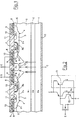
- Figure 1 shows a cross-sectional view of a portion of an Insulated Gate Bipolar Transistor according to the present invention.
- the device comprises a highly conductive semiconductor substrate 1 of a first conductivity type, which in the shown example corresponds to the P type; over the substrate 1 a highly conductive buffer layer 2 of the opposite conductivity type (N type in the shown example) is provided, and over the buffer layer 2 a lightly doped N type layer 3 is formed.
- N type in the shown example
- N type the opposite conductivity type
- N type layer 3 is formed inside the N type layer 3 a plurality of P type body regions 4 is formed; each body region preferably comprises a central heavily doped portion 5 surrounded by a more lightly doped channel portion 6.
- N type emitter regions 7 are formed.
- an insulated gate layer comprising a gate oxide layer 8 and a conductive gate layer 9, typically made of polysilicon.
- the insulated gate layer extends over the surface of the N type layer 3 between the body regions 4 and overlaps the channel portions 6 thereof.
- the insulated gate layer is covered by an insulating layer 10 wherein emitter contact openings are formed over the body regions 4 to allow for an emitter conductive layer 11 to contact the emitter regions 7 and the central portion 5 of each body region 4.
- the emitter conductive layer 11 is connected to an emitter terminal E of the device; at the rear surface of the substrate 1 a collector conductive layer 13 is provided, which is connected to a collector electrode C.
- the conductive gate layer 9 is electrically connected to a gate terminal G of the IGBT.
- a PNP bipolar junction transistor T1 ( Figure 2) formed by the regions 12, the N type layer 3 and the substrate 1 is provided in parallel to the collector and emitter electrodes C and E of the IGBT.
- Such a transistor T1 allows to reduce the hole current in the body regions 4 under the emitter regions 7, so that the voltage drop across the resistance Rb is lowered; the base-emitter voltage of the parasitic transistor T2 formed by the emitter regions 7, the body regions 4 and the N type layer 3 is reduced, and the triggering point of the parasitic thyristor inherently associated to the IGBT is elevated.
- Figure 3 is a top-plan view at the level of the front surface of layer 3 of a portion of an IGBT having a layout according to a first practical embodiment of the present invention.
- the body regions 4 have a square shape; inside each body region 4 an annular emitter region 7 is formed, defining an annular channel portion 6.
- the body regions 4 are arranged to form a bidimensional array in the N type layer 3.
- the P type regions 12 are formed in regions of the N type layer 3 comprised between the corners of four adjacent body regions 4, so that also the P type regions 12 form a bidimensional array.
- the cross-sectional view of Figure 1 corresponds to a section along line I-I of Figure 3.
- body regions 4 can also have shapes different from the square one, for example hexagonal.
- the Insulated Gate Bipolar Transistor according to the invention can be manufactured by means of anyone of the processes known in the art for the manufacturing Insulated Gate Bipolar Transistors: it is simply necessary to provide a step for the formation of the P type regions 12. Such a step need not to be a dedicated additional step: regions 12 can be advantageously formed simultaneously with the heavily doped portions 5 of the body regions 4.
- Figure 4 is a top-plan view similar to that of Figure 3, and shows a portion of an IGBT having a layout according to a second practical embodiment of the present invention.
- the body regions 4 are elongated, substantially rectangular stripes; inside each elongated body region 4 an elongated, annular emitter region 7 is formed, defining an elongated annular channel portion 6.
- Figure 4 is actually not in scale, because normally the body regions have a longitudinal dimension much larger than the transversal dimension.
- the body regions 4 are arranged in a bidimensional array, and the P type region 12 are formed in regions of the N type layer 3 comprised between the corners of four adjacent body regions 4.
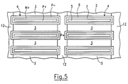
- Figure 5 is a top-plan view similar to that of Figure 4, and shows a portion of an IGBT having a layout according to a third embodiment of the present invention.
- the body regions 4 have a shape similar to that shown in Figure 4.
- the P type regions 12 have the form of elongated stripes extending orthogonally to the body stripes 4 in the portions of the N type layer 3 comprised between the body stripes 4; additionally, the body stripes are preferably merged at their ends with the P type stripes 12.
Abstract
An Insulated Gate Bipolar Transistor comprises a
semiconductor substrate (1) of a first conductivity type
forming a first electrode (C) of the device, a semiconductor
layer (3) of a second conductivity type superimposed over said
substrate (1), a plurality of body regions (4) of the first
conductivity type formed in the semiconductor layer (3), a
first doped region (7) of the second conductivity type formed
inside each body region (4), an insulated gate layer (8,9)
superimposed over portions of the semiconductor layer (3)
between the body regions (4) and forming a control electrode of
the device, a conductive layer (11) insulatively disposed over
the insulated gate layer (8,9) and contacting each body region
(4) and each doped region (7) formed therein, the conductive
layer (11) forming a second electrode (E) of the device. In
said portions of the semiconductor layer (3) between the body
regions (4) second doped regions (12) of the first conductivity
type are formed, and openings are provided in the insulated
gate layer (8,9) at said second doped regions (12) to allow the
conductive layer (11) to contact the second doped regions (12).
Description
The present invention relates to an Insulated Gate Bipolar
Transistor with a high dinamic ruggedness.
Known Insulated Gate Bipolar Transistors (IGBTs) comprise a
heavily doped semiconductor substrate of a first conductivity
type, for example of the P type, forming the collector of the
device, over which a lightly doped semiconductor layer of the
opposite conductivity type (N type) is formed; inside the N
type layer a plurality of elementary vertical MOSFETs is
formed, each comprising a P type body region and an N type
emitter region formed therein.
The IGBT is thus a four-layer device, and associated
therewith is a thyristor.
The most important feature of IGBTs over power MOSFETs is
the low output resistance, which is achieved thanks to the
conductivity modulation of the lightly doped N type layer by
means of the injection therein of minority carriers from the P
type substrate.
Conventionally, the performance of an IGBT is measured by
four electrical parameters: the collector-to-emitter saturation
voltage (VCESAT), which is directly related to the output
resistance and provides a measure of the energy dissipated by
the IGBT in on state, the breakdown voltage between collector
and emitter (BVCES), the latching current (Ilatch) and the
fall-time when the device is switched off (tfall), which
provides a measure of the energy dissipated by the IGBT when
switched off.
The optimization of a generic one of said parameters
generally lead to the degradation of one or more of the others;
for example, trying to improve tfall and Ilatch causes a
significant increase of VCESAT. In fact, it has been verified
that notwithstanding the conductivity modulation effect of the
lightly doped N type layer, the voltage drop caused by the
so-called JFET component of the output resistance is
substantial. This is due to the fact that not all of the
minority carriers injected into the lightly doped N type layer
from the substrate reach the surface of the device, some of
them recombining in the lightly doped N type layer before they
reach the surface thereof. For example, in a device with an N
type layer 60 um thick and having a dopant concentration of
1E14 atoms/cm3, thanks to the conductivity modulation effect
the dopant concentration in the N type layer at the junction
with the substrate is approximately 1E16 atoms/cm3 but only of
1E15 atoms/cm3 at the top surface of the N type layer.
To improve BVCES and Ilatch the distance between the
elementary vertical MOSFETs forming the IGBT (i.e., the
distance between the body regions) should be reduced; however,
this would cause a substantial increase of the JFET component
of the output resistance. On the contrary, increasing the
distance between the body regions would reduce the JFET
component of the output resistance, but at the cost of a
degradation of BVCES and Ilatch.
A low value of Ilatch means that the device is easily
subject to latch-up; latch-up can most easily occur during
switching: the voltage drop across the base and emitter of the
parasitic NPN transistor, caused by the hole current flowing in
the body region under the emitter region, turns the parasitic
NPN transistor on, thus triggering the parasitic thyristor on.
The voltage drop across the emitter and base of the NPN
parasitic transistor depends on the resistance of the body
region under the emitter region, and on the current of holes
which, injected into the N type layer from the substrate, are
collected by the body region of the IGBT. Triggering on of the
parasitic thyristor can also lead to the distruction of the
IGBT.
In view of the state of the art described, it is an object
of the present invention to provide an IGBT structure having a
high ruggedness, i.e. a high Ilatch value even in switching
conditions, achieved not at the expense of a deterioration of
the other electrical parameters characterizing the performance
of the device.
According to the present invention, such object is achived
by means of an Insulated Gate Bipolar Transistor comprising a
semiconductor substrate of a first conductivity type forming a
first electrode of the device, a semiconductor layer of a
second conductivity type superimposed over said substrate, a
plurality of body regions of the first conductivity type formed
in the semiconductor layer, a first doped region of the second
conductivity type formed inside each body region, an insulated
gate layer superimposed over portions of the semiconductor
layer between the body regions and forming a control electrode
of the device, a conductive layer insulatively disposed over
the insulated gate layer and contacting each body region and
each doped region formed therein, the conductive layer forming
a second electrode of the device, characterized in that in said
portions of the semiconductor layer between the body regions
second doped regions of the first conductivity type are formed,
and openings are provided in the insulated gate layer at said
second doped regions to allow the conductive layer to contact
the second doped regions.
Thanks to the fact that said second doped regions of the
first conductivity type are provided in the portions of the
second conductivity type semiconductor layer between the body
regions, and thanks to the fact that said second doped regions
are electrically connected to the body regions and to the
emitter regions of the IGBT, each elementary IGBT is shunted by
a bipolar junction transistor (BJT) formed by the second doped
region, the semiconductor layer and the substrate; such a BJT
provides a current path parallel to that of the parasitic
transistor formed by the first doped regions, the body regions
and the semiconductor layer, thus subtracting current
therefrom; the voltage drop across the base-emitter junction of
said parasitic transistor is thus reduced, and the triggering
point of the parasitic thyristor is elevated.
These and other features of the present invention will be
made apparent by the following detailed description of some
particular embodiments thereof, illustrated as non-limiting
examples in the annexed drawings, wherein:
Figure 1 shows a cross-sectional view of a portion of an
Insulated Gate Bipolar Transistor according to the present
invention. The device comprises a highly conductive
semiconductor substrate 1 of a first conductivity type, which
in the shown example corresponds to the P type; over the
substrate 1 a highly conductive buffer layer 2 of the opposite
conductivity type (N type in the shown example) is provided,
and over the buffer layer 2 a lightly doped N type layer 3 is
formed. Inside the N type layer 3 a plurality of P type body
regions 4 is formed; each body region preferably comprises a
central heavily doped portion 5 surrounded by a more lightly
doped channel portion 6. Inside each body region 4 heavily
doped N type emitter regions 7 are formed.
Over the surface of the N type layer 3 (the front surface of
the device) an insulated gate layer is provided comprising a
gate oxide layer 8 and a conductive gate layer 9, typically
made of polysilicon. The insulated gate layer extends over the
surface of the N type layer 3 between the body regions 4 and
overlaps the channel portions 6 thereof. The insulated gate
layer is covered by an insulating layer 10 wherein emitter
contact openings are formed over the body regions 4 to allow
for an emitter conductive layer 11 to contact the emitter
regions 7 and the central portion 5 of each body region 4.
The emitter conductive layer 11 is connected to an emitter
terminal E of the device; at the rear surface of the substrate
1 a collector conductive layer 13 is provided, which is
connected to a collector electrode C. The conductive gate layer
9 is electrically connected to a gate terminal G of the IGBT.
The structure described up to now is per-se conventional.
According to the present invention, in the portions of the N
type layer 3 between adjacent body regions 4 heavily doped P
type regions 12 are formed; openings are provided in the
insulated gate layer 8, 9 and in the overlying insulating layer
10 over the P type regions 12, so as to allow the emitter
conductive layer 11 to contact the P type regions 12.
Thanks to the provision of the P type regions 12,
electrically connected to the emitter regions 7 and to the
central portions 5 of the body regions 4, a PNP bipolar
junction transistor T1 (Figure 2) formed by the regions 12, the
N type layer 3 and the substrate 1 is provided in parallel to
the collector and emitter electrodes C and E of the IGBT. Such
a transistor T1 allows to reduce the hole current in the body
regions 4 under the emitter regions 7, so that the voltage drop
across the resistance Rb is lowered; the base-emitter voltage
of the parasitic transistor T2 formed by the emitter regions 7,
the body regions 4 and the N type layer 3 is reduced, and the
triggering point of the parasitic thyristor inherently
associated to the IGBT is elevated.
Figure 3 is a top-plan view at the level of the front
surface of layer 3 of a portion of an IGBT having a layout
according to a first practical embodiment of the present
invention. In this embodiment, the body regions 4 have a square
shape; inside each body region 4 an annular emitter region 7 is
formed, defining an annular channel portion 6. The body regions
4 are arranged to form a bidimensional array in the N type
layer 3. The P type regions 12 are formed in regions of the N
type layer 3 comprised between the corners of four adjacent
body regions 4, so that also the P type regions 12 form a
bidimensional array. The cross-sectional view of Figure 1
corresponds to a section along line I-I of Figure 3.
It is apparent that the body regions 4 can also have shapes
different from the square one, for example hexagonal.
The Insulated Gate Bipolar Transistor according to the
invention can be manufactured by means of anyone of the
processes known in the art for the manufacturing Insulated Gate
Bipolar Transistors: it is simply necessary to provide a step
for the formation of the P type regions 12. Such a step need
not to be a dedicated additional step: regions 12 can be
advantageously formed simultaneously with the heavily doped
portions 5 of the body regions 4.
Figure 4 is a top-plan view similar to that of Figure 3, and
shows a portion of an IGBT having a layout according to a
second practical embodiment of the present invention. In this
embodiment, the body regions 4 are elongated, substantially
rectangular stripes; inside each elongated body region 4 an
elongated, annular emitter region 7 is formed, defining an
elongated annular channel portion 6. Figure 4 is actually not
in scale, because normally the body regions have a longitudinal
dimension much larger than the transversal dimension. As in the
case of Figure 3, the body regions 4 are arranged in a
bidimensional array, and the P type region 12 are formed in
regions of the N type layer 3 comprised between the corners of
four adjacent body regions 4.
Figure 5 is a top-plan view similar to that of Figure 4, and
shows a portion of an IGBT having a layout according to a third
embodiment of the present invention. In this embodiment the
body regions 4 have a shape similar to that shown in Figure 4.
However, differently from the embodiment of Figure 4, the P
type regions 12 have the form of elongated stripes extending
orthogonally to the body stripes 4 in the portions of the N
type layer 3 comprised between the body stripes 4;
additionally, the body stripes are preferably merged at their
ends with the P type stripes 12.
Claims (8)
- Insulated Gate Bipolar Transistor comprising a semiconductor substrate (1) of a first conductivity type forming a first electrode (C) of the device, a semiconductor layer (3) of a second conductivity type superimposed over said substrate (1), a plurality of body regions (4) of the first conductivity type formed in the semiconductor layer (3), a first doped region (7) of the second conductivity type formed inside each body region (4), an insulated gate layer (8,9) superimposed over portions of the semiconductor layer (3) between the body regions (4) and forming a control electrode of the device, a conductive layer (11) insulatively disposed over the insulated gate layer (8,9) and contacting each body region (4) and each doped region (7) formed therein, the conductive layer (11) forming a second electrode (E) of the device, characterized in that in said portions of the semiconductor layer (3) between the body regions (4) second doped regions (12) of the first conductivity type are formed, and openings are provided in the insulated gate layer (8,9) at said second doped regions (12) to allow the conductive layer (11) to contact the second doped regions (12).
- Insulated Gate Bipolar Transistor according to claim 1, characterized in that said body regions (4) have a polygonal layout and are arranged in a bidimensional array, said second doped regions (12) being formed in portions of the semiconductor layer (3) comprised between groups of four adjacent body regions (4).
- Insulated Gate Bipolar Transistor according to claim 1, characterized in that said body regions (4) are elongated stripes and are arranged in a bidimensional array, said second doped regions (12) being formed in portions of the semiconductor layer (3) comprised between groups of four adjacent body regions.
- Insulated Gate Bipolar Transistor according to claim 1, characterized in that said body regions (4) are elongated stripes having two elongated sides and two short sides, and are arranged in a bidimensional array, said second doped regions (12) being elongated stripes formed in portions of the semiconductor layer (3) comprised between the body regions (4) and extending perpendicularly to the elongated sides of the body regions.
- Insulated Gate Bipolar Transistor according to claim 4, characterized in that the body regions are merged, at their short sides, with the second doped regions (12).
- Insulated Gate Bipolar Transistor according to anyone of the preceding claims, characterized in that between the semiconductor substrate (1) and the semiconductor layer (3) a heavily doped layer (2) of the second conductivity type is provided.
- Insulated Gate Bipolar Transistor according to anyone of the preceding claims, characterized in that said first conductivity type is the P type, and said second conductivity type is the N type.
- Insulated Gate Bipolar Transistor according to anyone of claims 1 to 6, characterized in that said first conductivity type is the N type, and said second conductivity type is the P type.
Priority Applications (3)
| Application Number | Priority Date | Filing Date | Title |
|---|---|---|---|
| EP97830108A EP0865085A1 (en) | 1997-03-11 | 1997-03-11 | Insulated gate bipolar transistor with high dynamic ruggedness |
| US09/034,391 US6169300B1 (en) | 1997-03-11 | 1998-03-04 | Insulated gate bipolar transistor with high dynamic ruggedness |
| JP10057946A JPH10290011A (en) | 1997-03-11 | 1998-03-10 | Insulating gate bipolar transistor |
Applications Claiming Priority (1)
| Application Number | Priority Date | Filing Date | Title |
|---|---|---|---|
| EP97830108A EP0865085A1 (en) | 1997-03-11 | 1997-03-11 | Insulated gate bipolar transistor with high dynamic ruggedness |
Publications (1)
| Publication Number | Publication Date |
|---|---|
| EP0865085A1 true EP0865085A1 (en) | 1998-09-16 |
Family
ID=8230592
Family Applications (1)
| Application Number | Title | Priority Date | Filing Date |
|---|---|---|---|
| EP97830108A Withdrawn EP0865085A1 (en) | 1997-03-11 | 1997-03-11 | Insulated gate bipolar transistor with high dynamic ruggedness |
Country Status (3)
| Country | Link |
|---|---|
| US (1) | US6169300B1 (en) |
| EP (1) | EP0865085A1 (en) |
| JP (1) | JPH10290011A (en) |
Cited By (24)
| Publication number | Priority date | Publication date | Assignee | Title |
|---|---|---|---|---|
| DE19904103A1 (en) * | 1999-02-02 | 2000-08-10 | Siemens Ag | Insulated gate bipolar transistor with improved on-state voltage |
| WO2009038610A1 (en) * | 2007-09-18 | 2009-03-26 | Cree, Inc. | Insulated gate bipolar conduction transistors (ibcts) and related methods of fabrication |
| US8193848B2 (en) | 2009-06-02 | 2012-06-05 | Cree, Inc. | Power switching devices having controllable surge current capabilities |
| US8294507B2 (en) | 2009-05-08 | 2012-10-23 | Cree, Inc. | Wide bandgap bipolar turn-off thyristor having non-negative temperature coefficient and related control circuits |
| US8330244B2 (en) | 2006-08-01 | 2012-12-11 | Cree, Inc. | Semiconductor devices including Schottky diodes having doped regions arranged as islands and methods of fabricating same |
| US8354690B2 (en) | 2009-08-31 | 2013-01-15 | Cree, Inc. | Solid-state pinch off thyristor circuits |
| US8415671B2 (en) | 2010-04-16 | 2013-04-09 | Cree, Inc. | Wide band-gap MOSFETs having a heterojunction under gate trenches thereof and related methods of forming such devices |
| US8432012B2 (en) | 2006-08-01 | 2013-04-30 | Cree, Inc. | Semiconductor devices including schottky diodes having overlapping doped regions and methods of fabricating same |
| US8541787B2 (en) | 2009-07-15 | 2013-09-24 | Cree, Inc. | High breakdown voltage wide band-gap MOS-gated bipolar junction transistors with avalanche capability |
| US8618582B2 (en) | 2011-09-11 | 2013-12-31 | Cree, Inc. | Edge termination structure employing recesses for edge termination elements |
| US8629509B2 (en) | 2009-06-02 | 2014-01-14 | Cree, Inc. | High voltage insulated gate bipolar transistors with minority carrier diverter |
| US8653534B2 (en) | 2008-05-21 | 2014-02-18 | Cree, Inc. | Junction Barrier Schottky diodes with current surge capability |
| US8664665B2 (en) | 2011-09-11 | 2014-03-04 | Cree, Inc. | Schottky diode employing recesses for elements of junction barrier array |
| US8680587B2 (en) | 2011-09-11 | 2014-03-25 | Cree, Inc. | Schottky diode |
| US8710510B2 (en) | 2006-08-17 | 2014-04-29 | Cree, Inc. | High power insulated gate bipolar transistors |
| US8835987B2 (en) | 2007-02-27 | 2014-09-16 | Cree, Inc. | Insulated gate bipolar transistors including current suppressing layers |
| US9029945B2 (en) | 2011-05-06 | 2015-05-12 | Cree, Inc. | Field effect transistor devices with low source resistance |
| US9117739B2 (en) | 2010-03-08 | 2015-08-25 | Cree, Inc. | Semiconductor devices with heterojunction barrier regions and methods of fabricating same |
| US9142662B2 (en) | 2011-05-06 | 2015-09-22 | Cree, Inc. | Field effect transistor devices with low source resistance |
| US9373617B2 (en) | 2011-09-11 | 2016-06-21 | Cree, Inc. | High current, low switching loss SiC power module |
| DE102005063580B3 (en) * | 2005-11-09 | 2017-01-05 | Infineon Technologies Ag | Power IGBT with increased robustness |
| US9640617B2 (en) | 2011-09-11 | 2017-05-02 | Cree, Inc. | High performance power module |
| US9673283B2 (en) | 2011-05-06 | 2017-06-06 | Cree, Inc. | Power module for supporting high current densities |
| CN108022973A (en) * | 2017-10-24 | 2018-05-11 | 全球能源互联网研究院 | A kind of integrated transoid MOS insulated gate bipolar transistor structures and preparation method thereof |
Families Citing this family (17)
| Publication number | Priority date | Publication date | Assignee | Title |
|---|---|---|---|---|
| KR100297705B1 (en) * | 1999-03-29 | 2001-10-29 | 김덕중 | Power semiconductor device having low on-resistance and high breakdown volatage |
| US6897682B2 (en) * | 2002-06-06 | 2005-05-24 | International Rectifier Corporation | MOSgate driver integrated circuit with adaptive dead time |
| JP5011634B2 (en) * | 2003-08-29 | 2012-08-29 | 富士電機株式会社 | Semiconductor device and bidirectional switch element using the semiconductor device |
| KR100906555B1 (en) * | 2007-08-30 | 2009-07-07 | 주식회사 동부하이텍 | Insulated gate bipolar transistor and Method for Manufacturing the same |
| US8643055B2 (en) * | 2007-09-26 | 2014-02-04 | Stmicroelectronics N.V. | Series current limiter device |
| EP3447803A3 (en) * | 2007-09-26 | 2019-06-19 | STMicroelectronics N.V. | Adjustable field effect rectifier |
| US8148748B2 (en) * | 2007-09-26 | 2012-04-03 | Stmicroelectronics N.V. | Adjustable field effect rectifier |
| KR100934797B1 (en) | 2007-12-27 | 2009-12-31 | 주식회사 동부하이텍 | Insulated Gate Bipolar Transistor and Manufacturing Method Thereof |
| WO2010080855A2 (en) | 2009-01-06 | 2010-07-15 | Lakota Technologies Inc. | Self-bootstrapping field effect diode structures and methods |
| US9530844B2 (en) * | 2012-12-28 | 2016-12-27 | Cree, Inc. | Transistor structures having reduced electrical field at the gate oxide and methods for making same |
| US10115815B2 (en) | 2012-12-28 | 2018-10-30 | Cree, Inc. | Transistor structures having a deep recessed P+ junction and methods for making same |
| US9312371B2 (en) * | 2014-07-24 | 2016-04-12 | Globalfoundries Inc. | Bipolar junction transistors and methods of fabrication |
| US10600871B2 (en) * | 2016-05-23 | 2020-03-24 | General Electric Company | Electric field shielding in silicon carbide metal-oxide-semiconductor (MOS) device cells using body region extensions |
| US11489069B2 (en) | 2017-12-21 | 2022-11-01 | Wolfspeed, Inc. | Vertical semiconductor device with improved ruggedness |
| US10615274B2 (en) | 2017-12-21 | 2020-04-07 | Cree, Inc. | Vertical semiconductor device with improved ruggedness |
| CN114678277B (en) * | 2022-05-27 | 2022-08-16 | 深圳平创半导体有限公司 | Split gate planar MOSFET with P + shielding region implanted at center and manufacturing method thereof |
| CN116190446B (en) * | 2022-12-20 | 2023-12-08 | 瑶芯微电子科技(上海)有限公司 | Silicon carbide-based MOSFET device with high reliability and manufacturing method thereof |
Citations (7)
| Publication number | Priority date | Publication date | Assignee | Title |
|---|---|---|---|---|
| EP0132861A1 (en) * | 1983-06-13 | 1985-02-13 | Koninklijke Philips Electronics N.V. | Semiconductor device comprising a field effect transistor |
| FR2575334A1 (en) * | 1984-12-21 | 1986-06-27 | Radiotechnique Compelec | MOS device whose source regions are arranged in parallel bands, and method for obtaining it |
| US4644637A (en) * | 1983-12-30 | 1987-02-24 | General Electric Company | Method of making an insulated-gate semiconductor device with improved shorting region |
| JPS63164473A (en) * | 1986-12-26 | 1988-07-07 | Fujitsu Ltd | Semiconductor device |
| US4801986A (en) * | 1987-04-03 | 1989-01-31 | General Electric Company | Vertical double diffused metal oxide semiconductor VDMOS device with increased safe operating area and method |
| FR2641417A1 (en) * | 1988-12-29 | 1990-07-06 | Fuji Electric Co Ltd | MOS TYPE SEMICONDUCTOR DEVICE |
| EP0536668A2 (en) * | 1991-10-07 | 1993-04-14 | Nippondenso Co., Ltd. | Vertical semiconductor device |
Family Cites Families (6)
| Publication number | Priority date | Publication date | Assignee | Title |
|---|---|---|---|---|
| DE3103444A1 (en) * | 1981-02-02 | 1982-10-21 | Siemens AG, 1000 Berlin und 8000 München | VERTICAL MIS FIELD EFFECT TRANSISTOR WITH SMALL THROUGH RESISTANCE |
| EP0416805B1 (en) * | 1989-08-30 | 1996-11-20 | Siliconix, Inc. | Transistor with voltage clamp |
| JPH04132264A (en) | 1990-09-21 | 1992-05-06 | Shindengen Electric Mfg Co Ltd | Insulating gate type field effect transistor |
| US5321281A (en) * | 1992-03-18 | 1994-06-14 | Mitsubishi Denki Kabushiki Kaisha | Insulated gate semiconductor device and method of fabricating same |
| JPH07240520A (en) * | 1994-03-01 | 1995-09-12 | Fuji Electric Co Ltd | Insulated gate type bipolar transistor |
| US5559355A (en) * | 1994-03-04 | 1996-09-24 | Fuji Electric Co., Ltd. | Vertical MOS semiconductor device |
-
1997
- 1997-03-11 EP EP97830108A patent/EP0865085A1/en not_active Withdrawn
-
1998
- 1998-03-04 US US09/034,391 patent/US6169300B1/en not_active Expired - Lifetime
- 1998-03-10 JP JP10057946A patent/JPH10290011A/en active Pending
Patent Citations (7)
| Publication number | Priority date | Publication date | Assignee | Title |
|---|---|---|---|---|
| EP0132861A1 (en) * | 1983-06-13 | 1985-02-13 | Koninklijke Philips Electronics N.V. | Semiconductor device comprising a field effect transistor |
| US4644637A (en) * | 1983-12-30 | 1987-02-24 | General Electric Company | Method of making an insulated-gate semiconductor device with improved shorting region |
| FR2575334A1 (en) * | 1984-12-21 | 1986-06-27 | Radiotechnique Compelec | MOS device whose source regions are arranged in parallel bands, and method for obtaining it |
| JPS63164473A (en) * | 1986-12-26 | 1988-07-07 | Fujitsu Ltd | Semiconductor device |
| US4801986A (en) * | 1987-04-03 | 1989-01-31 | General Electric Company | Vertical double diffused metal oxide semiconductor VDMOS device with increased safe operating area and method |
| FR2641417A1 (en) * | 1988-12-29 | 1990-07-06 | Fuji Electric Co Ltd | MOS TYPE SEMICONDUCTOR DEVICE |
| EP0536668A2 (en) * | 1991-10-07 | 1993-04-14 | Nippondenso Co., Ltd. | Vertical semiconductor device |
Non-Patent Citations (1)
| Title |
|---|
| PATENT ABSTRACTS OF JAPAN vol. 012, no. 425 (E - 681) 10 November 1988 (1988-11-10) * |
Cited By (35)
| Publication number | Priority date | Publication date | Assignee | Title |
|---|---|---|---|---|
| DE19904103B4 (en) * | 1999-02-02 | 2005-04-14 | Infineon Technologies Ag | IGBT with improved forward voltage |
| DE19904103A1 (en) * | 1999-02-02 | 2000-08-10 | Siemens Ag | Insulated gate bipolar transistor with improved on-state voltage |
| DE102005063580B3 (en) * | 2005-11-09 | 2017-01-05 | Infineon Technologies Ag | Power IGBT with increased robustness |
| US8330244B2 (en) | 2006-08-01 | 2012-12-11 | Cree, Inc. | Semiconductor devices including Schottky diodes having doped regions arranged as islands and methods of fabricating same |
| US8432012B2 (en) | 2006-08-01 | 2013-04-30 | Cree, Inc. | Semiconductor devices including schottky diodes having overlapping doped regions and methods of fabricating same |
| US8710510B2 (en) | 2006-08-17 | 2014-04-29 | Cree, Inc. | High power insulated gate bipolar transistors |
| US9548374B2 (en) | 2006-08-17 | 2017-01-17 | Cree, Inc. | High power insulated gate bipolar transistors |
| US8835987B2 (en) | 2007-02-27 | 2014-09-16 | Cree, Inc. | Insulated gate bipolar transistors including current suppressing layers |
| US9064840B2 (en) | 2007-02-27 | 2015-06-23 | Cree, Inc. | Insulated gate bipolar transistors including current suppressing layers |
| WO2009038610A1 (en) * | 2007-09-18 | 2009-03-26 | Cree, Inc. | Insulated gate bipolar conduction transistors (ibcts) and related methods of fabrication |
| US7687825B2 (en) | 2007-09-18 | 2010-03-30 | Cree, Inc. | Insulated gate bipolar conduction transistors (IBCTS) and related methods of fabrication |
| US8653534B2 (en) | 2008-05-21 | 2014-02-18 | Cree, Inc. | Junction Barrier Schottky diodes with current surge capability |
| US8294507B2 (en) | 2009-05-08 | 2012-10-23 | Cree, Inc. | Wide bandgap bipolar turn-off thyristor having non-negative temperature coefficient and related control circuits |
| US8193848B2 (en) | 2009-06-02 | 2012-06-05 | Cree, Inc. | Power switching devices having controllable surge current capabilities |
| US8629509B2 (en) | 2009-06-02 | 2014-01-14 | Cree, Inc. | High voltage insulated gate bipolar transistors with minority carrier diverter |
| US8541787B2 (en) | 2009-07-15 | 2013-09-24 | Cree, Inc. | High breakdown voltage wide band-gap MOS-gated bipolar junction transistors with avalanche capability |
| US8354690B2 (en) | 2009-08-31 | 2013-01-15 | Cree, Inc. | Solid-state pinch off thyristor circuits |
| US9117739B2 (en) | 2010-03-08 | 2015-08-25 | Cree, Inc. | Semiconductor devices with heterojunction barrier regions and methods of fabricating same |
| US9595618B2 (en) | 2010-03-08 | 2017-03-14 | Cree, Inc. | Semiconductor devices with heterojunction barrier regions and methods of fabricating same |
| US8415671B2 (en) | 2010-04-16 | 2013-04-09 | Cree, Inc. | Wide band-gap MOSFETs having a heterojunction under gate trenches thereof and related methods of forming such devices |
| US9673283B2 (en) | 2011-05-06 | 2017-06-06 | Cree, Inc. | Power module for supporting high current densities |
| US9142662B2 (en) | 2011-05-06 | 2015-09-22 | Cree, Inc. | Field effect transistor devices with low source resistance |
| US9029945B2 (en) | 2011-05-06 | 2015-05-12 | Cree, Inc. | Field effect transistor devices with low source resistance |
| US9231122B2 (en) | 2011-09-11 | 2016-01-05 | Cree, Inc. | Schottky diode |
| US8618582B2 (en) | 2011-09-11 | 2013-12-31 | Cree, Inc. | Edge termination structure employing recesses for edge termination elements |
| US9373617B2 (en) | 2011-09-11 | 2016-06-21 | Cree, Inc. | High current, low switching loss SiC power module |
| US8664665B2 (en) | 2011-09-11 | 2014-03-04 | Cree, Inc. | Schottky diode employing recesses for elements of junction barrier array |
| US9640617B2 (en) | 2011-09-11 | 2017-05-02 | Cree, Inc. | High performance power module |
| US8680587B2 (en) | 2011-09-11 | 2014-03-25 | Cree, Inc. | Schottky diode |
| US9865750B2 (en) | 2011-09-11 | 2018-01-09 | Cree, Inc. | Schottky diode |
| US10141302B2 (en) | 2011-09-11 | 2018-11-27 | Cree, Inc. | High current, low switching loss SiC power module |
| US10153364B2 (en) | 2011-09-11 | 2018-12-11 | Cree, Inc. | Power module having a switch module for supporting high current densities |
| US11024731B2 (en) | 2011-09-11 | 2021-06-01 | Cree, Inc. | Power module for supporting high current densities |
| US11171229B2 (en) | 2011-09-11 | 2021-11-09 | Cree, Inc. | Low switching loss high performance power module |
| CN108022973A (en) * | 2017-10-24 | 2018-05-11 | 全球能源互联网研究院 | A kind of integrated transoid MOS insulated gate bipolar transistor structures and preparation method thereof |
Also Published As
| Publication number | Publication date |
|---|---|
| JPH10290011A (en) | 1998-10-27 |
| US6169300B1 (en) | 2001-01-02 |
Similar Documents
| Publication | Publication Date | Title |
|---|---|---|
| US6169300B1 (en) | Insulated gate bipolar transistor with high dynamic ruggedness | |
| KR100218873B1 (en) | Insulated gate semiconductor device and manufacturing method thereof | |
| US6580108B1 (en) | Insulated gate bipolar transistor decreasing the gate resistance | |
| US5089864A (en) | Insulated gate type semiconductor device | |
| US6747295B2 (en) | Semiconductor device with trench gate | |
| JP6320808B2 (en) | Trench MOS semiconductor device | |
| JP3243902B2 (en) | Semiconductor device | |
| US6262470B1 (en) | Trench-type insulated gate bipolar transistor and method for making the same | |
| EP0697739B1 (en) | Insulated gate bipolar transistor | |
| US6133607A (en) | Semiconductor device | |
| CN108417614B (en) | Semiconductor device with a plurality of semiconductor chips | |
| KR20090008112A (en) | Semiconductor device | |
| JP7210342B2 (en) | semiconductor equipment | |
| US20040256659A1 (en) | MOS-gated transistor with improved UIS capability | |
| JP3338185B2 (en) | Semiconductor device | |
| CN109075199A (en) | Semiconductor device | |
| US8067797B2 (en) | Variable threshold trench IGBT with offset emitter contacts | |
| JP6610696B2 (en) | Trench MOS semiconductor device | |
| JPH0716009B2 (en) | Lateral insulated gate bipolar transistor | |
| JP4746169B2 (en) | Power semiconductor device and driving method thereof | |
| JP2023138654A (en) | Semiconductor device and semiconductor circuit | |
| US11855077B2 (en) | Semiconductor device | |
| JP6391863B2 (en) | Trench MOS semiconductor device | |
| JP3905271B2 (en) | Semiconductor device | |
| JP2004363477A (en) | Insulating gate type semiconductor device |
Legal Events
| Date | Code | Title | Description |
|---|---|---|---|
| PUAI | Public reference made under article 153(3) epc to a published international application that has entered the european phase |
Free format text: ORIGINAL CODE: 0009012 |
|
| AK | Designated contracting states |
Kind code of ref document: A1 Designated state(s): DE FR GB IT |
|
| AX | Request for extension of the european patent |
Free format text: AL;LT;LV;RO;SI |
|
| 17P | Request for examination filed |
Effective date: 19990312 |
|
| AKX | Designation fees paid |
Free format text: DE FR GB IT |
|
| RBV | Designated contracting states (corrected) |
Designated state(s): DE FR GB IT |
|
| STAA | Information on the status of an ep patent application or granted ep patent |
Free format text: STATUS: THE APPLICATION IS DEEMED TO BE WITHDRAWN |
|
| 18D | Application deemed to be withdrawn |
Effective date: 20060306 |