The present invention relates to semiconductor processing.
One of the primary steps in fabricating modern semiconductor
devices is forming a dielectric layer on a semiconductor substrate. As is well
known, such a dielectric layer can be deposited by chemical vapor deposition
(CVD). In a conventional thermal CVD process, reactive gases are supplied to
the substrate surface where heat-induced chemical reactions (homogeneous
or heterogeneous) take place to produce a desired film. In a conventional
plasma process, a controlled plasma is formed to decompose and/or energize
reactive species to produce the desired film. In general, reaction rates in
thermal and plasma processes may be controlled by controlling one or more
of the following: temperature, pressure, and reactant gas flow rate.
Semiconductor device geometries have dramatically decreased
in size since such devices were first introduced several decades ago. Since
then, integrated circuits have generally followed the two-year/half-size rule
(often called "Moore's Law") which means that the number of devices which
will fit on a chip doubles every two years. Today's wafer fabrication plants
are routinely producing 0.5 mm and even 0.35 mm feature size devices, and
tomorrow's plants soon will be producing devices having even smaller feature
sizes. As device feature sizes become smaller and integration density
increases, issues not previously considered crucial by the industry are
becoming of greater concern. In particular, devices with increasingly high
integration density have features with high (for example, greater than about
3:1 or 4:1) aspect ratios. (Aspect ratio is defined as the height-to-spacing
ratio of two adjacent steps.)
Increasingly stringent requirements for processes in fabricating
these high integration devices are needed in order to produce high quality
devices, and conventional substrate processing systems are becoming
inadequate to meeting these requirements. One requirement is that the
dielectric films formed in the process of fabricating such devices need to be
uniformly deposited over these high aspect ratio features without leaving
substantial gaps or voids. Another requirement is that these films need to
exhibit low shrinkage so that subsequent heating and/or wet etching steps do
not cause voids to open up in the deposited film. However, conventional
substrate processing systems that typically deposit dielectric films at
temperatures less than about 450°C are unable to produce low moisture films
having good gap-filling capabilities without opening substantial voids in
subsequent heating and/or wet etching steps. As is well known, these gaps or
voids may contribute to device performance unreliability and other problems.
Dielectric films used, for example, as PMD or IMD layers in such devices
need good high aspect ratio gap-fill capability to avoid problems caused by
these gaps or voids. A further requirement is that metal contamination into
the wafer during the processing steps be minimized to avoid short circuits
and other problems in the devices. As is well known, conventional substrate
processing systems using in situ plasma during processing experience
physical sputtering of ions which attack chamber surfaces, such as aluminum
walls, resulting in metal contamination of the substrate. Use of in situ
plasma is therefore undesirable. An improved substrate processing system,
which does not use in situ plasma, is needed to provide dielectric films with
the desired characteristics of low moisture, high density, low shrinkage, good
high aspect ratio gap-filling capability.
In addition to meeting these stringent requirements, substrate
processing systems must be able to meet the higher demands for forming
ultra-shallow doped regions, which are necessary for high integration devices
with shrinking device geometries. With the advent of smaller device
geometries, ultra-shallow doped regions in semiconductors are needed for
various applications including, for example, source/drain junctions, channel
stop diffusions for shallow trench isolation, etc. For example, MOS devices
with channel lengths of less than 0.8 mm often require source/drain
junctions having depths less than about 250 nanometers (nm) for adequate
device performance. For transistors separated by trench isolation structures
of about 0.35 mm depth, ultra-shallow channel stop regions having a depth
on the order of hundreds of nm are usually required. For applications
requiring ultra-shallow doped regions, it is important to provide uniform
dopant distribution in the doped regions and good control of junction depth.
Current approaches to forming ultra-shallow doped regions,
such as ion implantation and gaseous diffusion, are inadequate in some
applications. With these current approaches, the ability to control dopant
distribution and junction depth is limited, especially as the doped regions
become shallower. With an approach like ion implantation, controlling
dopant distribution is made difficult due to the built-up concentration of ions
at the surface of the semiconductor material. Also, ion implantation causes
damage to the semiconductor surface, and methods for repairing this
substrate damage often make it more difficult to control dopant distribution
and junction depth for ultra-shallow doped regions. For example, ions
bombarded at relatively high energy levels have a tendency to tunnel or
channel through the semiconductor material and cause damage such as point
defects. These point defects, which may lead to irregular and nonuniform
junction depths, may be feed by annealing the implanted semiconductor
material at high temperatures (greater than about 900°C). Annealing the
implanted semiconductor material, however, may further increase the
junction depth beyond that desired. With an approach like gaseous diffusion,
controlling dopant distribution and junction depth is difficult to control in
forming ultra-shallow doped regions. As technology progresses to even
smaller geometry devices, an alternative approach that is able to control the
dopant uniformity and junction depth in ultra-shallow doped regions is
needed.
In forming ultra-shallow doped regions, one alternative
approach to the current approaches of ion implantation and gaseous diffusion
is the use of a doped dielectric film as a dopant diffusion source. In this
alternative approach, a doped dielectric film is deposited onto a substrate and
used as a source of dopants which are diffused into the substrate to form
ultra-shallow doped regions. For example, doped dielectric films are
deposited at temperatures less than 500°C in a deposition chamber, and
subsequently heated at temperatures greater than 500°C in a different
chamber, such as an annealing furnace, to perform the dopant diffusion to
form the doped region. Controlling thickness, uniformity, and moisture
content of the doped dielectric film is important in efficiently forming
ultra-shallow doped junctions in the semiconductor material. Specifically,
controlling the thickness and uniformity of the deposited doped dielectric
film provides some control over the amount of dopants available for
diffusion. Limiting the thickness of doped dielectric films used as diffusion
sources also helps to increase wafer throughput by saving deposition (and
subsequent etching) time. Moreover, a uniformly deposited film with even
dopant uniformity can provide a more controlled diffusion of dopants from
the film into the substrate. As is well known, moisture in doped dielectric
films reacts with dopants to bind them in a crystal structure, resulting in
fewer dopants available for diffusion into the substrate to form doped
regions. It is desirable to use doped dielectric films having a low moisture
content, since these films have more dopants available for use in the
diffusion.
Several problems are encountered with conventional substrate
processing systems when using a doped dielectric film as a dopant diffusion
source. One problem is that it is difficult to obtain a high degree of control
over film thickness and uniformity when using conventional systems to
deposit the doped dielectric film. Another problem is that it is often difficult
to ensure that adequate amounts of dopants in the doped dielectric film are
available for diffusion into the substrate to form the ultra-shallow doped
regions. A further problem is the existence of native oxides, which act as a
barrier layer preventing dopants from diffusing into the substrate from the
doped dielectric film, on substrate surfaces where the ultra-shallow doped
regions are to be formed. These problems are discussed in further detail
below.
Despite the advantages of using doped dielectric films as dopant
diffusion sources to form ultra-shallow doped regions, the problem of being
unable to control thickness and uniformity of the deposited doped dielectric
film when using conventional deposition systems is of particular concern for
two primary reasons. First, the inability to adequately control thickness and
uniformity of the deposited doped dielectric film using conventional methods
and apparatus undesirably results in a diminished ability to control the
dopant uniformity and junction depth of the ultra-shallow doped region
formed. For example, in a conventional sequential CVD chamber, a substrate
rests on a belt and travels through various portions of the chamber. In each
portion of the chamber, a layer having a certain thickness may be deposited.
Thickness of the deposited film may be controlled by changing the belt speed,
which provides limited control. Further, control over the thickness and
dopant uniformity of the films deposited on different wafers is difficult when
attempting to control film thickness and dopant concentration using belt
speed. That is, the thicknesses of the deposited films on different wafers may
vary and be unpredictable, leading to wafer-to-wafer unreliability. Second,
being able to control the thickness of the deposited doped dielectric film,
even for very thin films, is desirable for overall efficiency and increased wafer
throughput. However, conventional approaches have only been capable of
forming doped dielectric films with thicknesses on the order of thousands of
Angstroms (Å). Also, it may be difficult to maintain the thickness of the
deposited film as thin as possible using systems relying on belt speed to
control thickness of the deposited film. With thicker films deposited
conventionally, some dopants may take longer to diffuse into the substrate,
since they have greater distances to travel before reaching the semiconductor
material. Also, removal of such a thick film used as a dopant diffusion source
by etching or other technique often increases the total time to process the
wafer. With growing pressures on manufacturers to improve efficiency, it is
desirable to form the doped dielectric film as thin as possible in order to
decrease the time needed to deposit and then remove the film. It is desirable
to have a method and apparatus that can easily control the thickness and
dopant uniformity of a doped dielectric film (less than about 500 Å thick at
± 0.2 weight percentage dopant variation across the wafer) that is used as a
dopant diffusion source.
Another problem with using doped dielectric films as dopant
diffusion sources for ultra-shallow doped regions is that adequate amounts of
dopants must be available for diffusion into the substrate. Films with high
dopant concentration are often needed to provide adequate amounts of
dopants for uniform diffusion into the substrate to form ultra-shallow
junctions. However, moisture absorption and outgassing are two problems
relating to adequate dopant availability. Doped dielectric films, especially
those with high dopant concentrations, tend to absorb moisture shortly after
a wafer is exposed to ambient moisture in a clean room (e.g. when the wafer
is transferred from the deposition chamber after deposition of the doped
dielectric film to a different processing chamber for the next processing step
in a multiple-step process). The absorbed moisture (H2O) then reacts with
the dopants in the dielectric film, causing the film to crystallize. Due to the
crystal structure binding the dopants within the film, these dopants become
unavailable for diffusion into the substrate, even after a subsequent heating
of the wafer by rapid thermal processing or annealing in another chamber.
Moisture absorption thus reduces the amount of dopants for diffusion into
the substrate. In addition to the moisture absorption problem, outgassing of
dopants from the doped dielectric film also may occur in subsequent heating
steps. These dopants diffuse out of the film away from the substrate,
resulting in fewer dopants available to be diffused into the substrate to form
ultra-shallow doped regions.
Even if adequate dopants are available for diffusion, the
problem of native oxides remains an important consideration when using
doped dielectric films as diffusion sources. Native oxides existing on the
substrate surface where ultra-shallow doped regions are to be formed prevent
effective and uniform dopant diffusion into the silicon. Therefore, native
oxides, which act as a diffusion barrier layer to the dopants, need to be
removed. Removing native oxides has been done using conventional
techniques such as wet etching using liquid etchants, and dry etching using
an in situ plasma. However, using liquid etchants is often difficult to control
and may result in overetching the substrate. Substrates that have native
oxides cleaned by conventional methods such as wet etching have shelf lives
of less than about one week before native oxides begin to form again, making
it desirable to process the wafers shortly after the native oxides have been
removed. Using dry etching to remove native oxides with an in situ plasma
results in plasma damage to the surface of the substrate. In addition to
causing surface plasma damage, in situ plasma dry etching may undesirably
result in more metal contamination, as discussed earlier. Accordingly, it is
important to efficiently remove native oxides without damaging the
substrate surface so dopants may diffuse into the substrate uniformly for
ultra-shallow doped regions.
In addition to providing dense, low moisture dielectric films
having uniform thickness and high aspect ratio gap-filling capability with low
metal contamination, improved quality and overall efficiency in fabricating
integrated circuit devices is also important. An important way to improve
quality and overall efficiency in fabricating devices is to clean the chamber
effectively and economically. With growing pressures on manufacturers to
improve processing quality and overall efficiency, eliminating the total down-time
in a multiple-step process without compromising the quality of the
wafers has become increasingly important for saving both time and money.
During CVD processing, reactive gases released inside the processing
chamber form layers such as silicon oxides or nitrides on the surface of a
substrate being processed. Undesirable oxide deposition occurs elsewhere in
the CVD apparatus, such as in the area between the gas mixing box and gas
distribution manifold. Undesired oxide residues also may be deposited in or
around the exhaust channel and the walls of the processing chamber during
such CVD processes. Over time, failure to clean the residue from the CVD
apparatus often results in degraded, unreliable processes and defective
substrates. Without frequent cleaning procedures, impurities from the
residue built up in the CVD apparatus can migrate onto the substrate. The
problem of impurities causing damage to the devices on the substrate is of
particular concern with today's increasingly small device dimensions. Thus,
CVD system maintenance is important for the smooth operation of substrate
processing, as well as resulting in improved device yield and better product
performance.
Frequently, periodic chamber cleanings between processing of
every N wafers is needed to improve CVD system performance in producing
high quality devices. Providing an efficient, non-damaging clean of the
chamber and/or substrate is often able to enhance performance and quality
of the devices produced. In addition to improving the quality of the above-discussed
chamber cleanings (which are done without breaking the vacuum
seal), preventive maintenance chamber cleanings (where the vacuum seal is
broken by opening the chamber lid to physically wipe down the chamber) are
performed between multiple periodic chamber cleanings. Often, performing
the necessary preventive maintenance chamber cleanings involves opening
the chamber lid and any other chamber parts that might obstruct the lid,
which is a time-consuming procedure that interferes with normal production
processing.
In light of the above, improved methods, systems and apparatus
are needed for depositing dense, low moisture dielectric films with uniform
thicknesses and high aspect ratio gap-filling capabilities. Optimally, these
improved methods and apparatus will also provide a chamber clean with low
metal contamination. Improved methods and apparatus are also needed for
forming doped dielectric films as dopant diffusion sources for ultra-shallow
junctions. These methods and apparatus should be capable of efficiently
removing native oxides to ensure effective and uniform dopant diffusion from
the doped dielectric layer without causing significant surface damage to the
silicon wafer. Further, for some applications it is desirable to provide
multiple deposition and cleaning capabilities in a single chamber with a
simplified design to minimize the time consumed for different types of
cleanings. What is needed, therefore, are systems and methods that are
capable of high quality, efficient, high temperature deposition and efficient,
gentle cleaning. In particular, these systems and methods should be designed
to be compatible with processing requirements for forming devices with high
aspect ratio features, and for forming ultra-shallow doped regions.
It is the object of the invention to provide aa method and an
apparatus for processing a substrate whereby an efficient deposition of
dense, low moisture dielectric films with uniform thicknesses and high aspect
ratio gap-filling capabilities is possible..
According to embodiments the invention relates to a method
and apparatus for forming dielectric films over high aspect ratio features at
temperatures greater than about 500°C, with the dielectric films having low
moisture content and low shrinkage. Embodiments of the present invention
are particularly useful to deposit doped dielectric films, such as
borophosphosilicate glass (BPSG) films, borosilicate glass (BSG) films, or
phosphosilicate glass (PSG) films, and to form ultra-shallow doped regions
used, for example, as source/drain junctions or as channel stop diffusions in
shallow trench isolation. In addition, embodiments of the present invention
may also be used to deposit doped dielectric films used as premetal dielectric
(PMD) layers, intermetal dielectric (IMD) layers, or other dielectric layers.
Further embodiments of the present invention may further be used to
deposit undoped dielectric films, such as undoped silicate glass (USG) films
used as shallow trench isolation filling oxides, insulating layers, capping
layers, or other layers.
Embodiments of the invention provide methods and apparatus
for high temperature (at least about 500-800°C) processing of semiconductor
wafers. Embodiments of the present invention include systems, methods and
apparatus which enable multiple process steps to be performed in situ in the
same chamber to reduce total processing time and to ensure high quality
processing to produce high integration devices having high aspect ratio
features. Performing multiple process steps in the same chamber also
increases the control over process parameters, substantially reduces
moisture content in deposited films, and minimizes device damage due to
metal contamination or process residue contamination.
In particular, the embodiments of the invention provide high
temperature deposition, heating and efficient cleaning for forming dielectric
films having relatively thin film thicknesses. Embodiments of the invention
are particularly useful to deposit doped dielectric films, such as
borophosphosilicate glass (BPSG) films, borosilicate glass (BSG) films, or
phosphosilicate glass (PSG) films, and to form an ultra-shallow doped region
used, for example, as source/drain junctions or as channel stop diffusions in
shallow trench isolation. In addition, embodiments of the present invention
may also be used to deposit doped dielectric films used as premetal dielectric
(PMD) layers, intermetal dielectric (IMD) layers, or other dielectric layers.
Further embodiments of the invention may further be used to deposit
undoped dielectric films used as shallow trench isolation filling oxides,
insulating layers, capping layers, or other layers.
Embodiments of the method according to the invention include
depositing dielectric films by CVD on a substrate in a vacuum chamber
having a pressure between about 10-760 Torr (13,3 x 10² to 1 x 10⁵ Pa) to a
temperature greater than about 500°C. The substrate may be heated for a
variety of purposes, such as performing reflow of deposited dielectric layers
for planarization, or for driving in dopants from a deposited doped dielectric
layer. The process may be carried out in a single step (e.g., depositing and
reflowing the film on the wafer at temperatures greater than 500°C), or in
multiple steps (e.g., depositing the film on the wafer at temperatures less
than 500°C and then heating the film on the wafer after the film has been
deposited). In either case, high temperature processing is accomplished
without removing the wafer from the vacuum chamber, which
advantageously reduces moisture absorption in the dielectric film. The high
temperature processing also enables in situ deposition of doped dielectric
films with capping layers to advantageously reduce outgassing of dopants
from the doped film and lower moisture content. In a specific embodiment,
reactive gases are delivered to the substrate surface, where heat-induced
chemical reactions take place to produce the dielectric film. Additionally or
alternatively, a controlled plasma may be formed to facilitate the
decomposition of the reactive species.
In an embodiment of the invention, the dielectric film is a thin
doped film used as a dopant diffusion source for an ultra-shallow junction.
The film is deposited at temperatures greater than about 500°C onto the
substrate and heated to higher temperatures, usually greater than 600°C and
preferably greater than about 700°C, to diffuse dopants from the dielectric
layer to the underlying substrate. Performing the deposition and heating
steps in the same chamber provides better control of the thickness,
uniformity, and moisture content of the doped dielectric film. Improving the
moisture content of the film increases the amounts of available dopants in
the film, which is particularly advantageous for forming ultra-shallow
junctions in high integration devices.
In another preferred embodiment of the invention, a remote
plasma system is provided for etching undesired deposits on the inner walls
of the vacuum chamber and components of the apparatus, and for cleaning
native oxides and other residue from the semiconductor wafer prior to
processing. A gentle cleaning technique using a remote energy source is
preferably employed instead of a conventional in situ plasma process to lower
metal contamination. For example, the remote plasma system provides a
remote plasma and preferably fluorine radicals from the plasma are able to
enter the chamber, which is at high temperatures, and provide a gentle,
thermal cleaning of the chamber. With the remote plasma system, only
chemical reactions are utilized and the problem of physical sputtering effects
are eliminated. In contrast, with the use of an in situ plasma system,
sputtering effects attack aluminum chamber walls, which may then lead to
metal contamination in the processed wafer. In the thermal cleaning process
using the remote plasma system, the radicals directed into the chamber can
effectively clean unwanted deposits and residues from the surfaces in the
chamber while the plasma remains remote or exterior to the chamber.
Another advantage of the remote plasma system is that native oxides can be
efficiently removed from the wafer to effectively ensure effective and uniform
dopant diffusion from the doped dielectric layer without causing significant
surface damage to the silicon wafer. A further advantage of the remote
plasma system is that the system may also be configured for use to deposit
films by using different input gases as needed.
In a preferred embodiment of the invention, the remote plasma
cleaning system is a microwave plasma system configured to produce and
deliver a select species (such as fluorine, chlorine or other radicals) to the
processing chamber. The remote plasma system energizes gases by
microwave radiation to create a plasma with etching radicals. Specifically,
microwaves are created by a magnetron or other suitable energy source and
directed through a waveguide system to an applicator tube, where a plasma is
created. Reactive gases are then fed into the applicator tube and energized by
the microwave energy, which sustains the ionization of the ignited plasma to
produce a flow of radicals into the processing chamber. For cleaning, the
radicals interact with residue formed on the chamber walls to form reactant
gases that are suitably discharged form the chamber by an exhaust system.
The microwave plasma system may also be adapted to deposit plasma
enhanced CVD films by delivering deposition reactive gases into the
processing chamber.
In another preferred embodiment of the invention, the remote
plasma system includes an endpoint detection system for indicating when the
chamber cleaning has concluded. The lack of plasma in the chamber can
make it difficult, using conventional endpoint detection systems, to pinpoint
the time at which the cleaning has been completed (i.e., when the last process
gas residue in the chamber has reacted with the cleaning etchant so that it
can be discharged from the chamber). This is because conventional endpoint
detection systems typically rely on the use of a plasma within the chamber to
check emissions from the in situ plasma to determine the end of the cleaning
process. In the present invention, an endpoint detection assembly is coupled
to the gas outlet of the processing chamber to determine the endpoint of the
cleaning process by detecting changes in light intensity that occur due to
absorbance of light by the exhausted clean gas reactants, such as SiF4.
In yet another preferred embodiment of the present invention,
a method provides gettering of any adsorbed clean gases, such as fluorine
from the surface of chamber walls. According to the present invention, a first
cleaning gas containing fluorine is introduced into the processing chamber to
clean the processing chamber of deposition residue. A second cleaning gas is
then introduced into the processing chamber after the residue has been
removed with the first cleaning gas. The second cleaning gas removes
cleaning residue formed by the reaction between the first cleaning gas and
the interior surfaces of the processing chamber. Removing or gettering the
cleaning residue from the chamber provides a number of advantages. For
example, in a preferred embodiment of the present invention, fluorine
radicals are delivered into the processing chamber to remove residue, such as
silicon oxide, by forming a silicon-fluoride gas product which is pumped away
from chamber. After the fluorine-based chamber cleaning procedure, any
adsorbed fluorine on the surface of the chamber walls which might otherwise
interact with, or be incorporated into, the deposited film on the next wafer to
be processed is gettered. In an alternative embodiment, the gettering may be
performed by seasoning the chamber using microwave-generated atomic
oxygen and a silicon source to deposit a thin film of oxide onto the chamber
to trap any adsorbed fluorine and prevent contamination of the subsequently
deposited films.
The preferred embodiments of the invention also provide
various heat-resistant and process-compatible components for high
temperature processing. The system of the present invention includes a
vapor deposition apparatus having an enclosure assembly housing a
processing chamber. The apparatus includes a heating assembly having a
pedestal/heater for heating the wafer to temperatures up to about 500-800°C.
The pedestal preferably comprises a material that is substantially resistant
to reactions with the process gases and to deposition by the process gases at
temperatures of at least about 400°C, and preferably at temperatures up to
about 500-800°C. In addition, the pedestal preferably comprises a material
that is substantially resistant to etching at high temperatures (i.e., 500-800°C)
by the fluorine radicals introduced into the chamber during cleaning.
In an exemplary embodiment, the pedestal/heater comprises a resistive
heating element imbedded in a ceramic material, such as aluminum oxide or
preferably aluminum nitride.
The heating assembly of the preferred embodiments of the
present invention further includes a support shaft for supporting the
pedestal/heater within the chamber and for housing the necessary electrical
connections thereto. The support shaft preferably comprises a ceramic
material that is diffusion-bonded to the pedestal/heater to provide a vacuum
seal within the shaft. This vacuum seal allows the hollow interior of the shaft
to be maintained at ambient temperature and pressure during high
temperature processing, which protects the electrodes and other electrical
connections from corrosion from the process and clean gases within the
chamber. In addition, providing ambient pressure within the shaft minimizes
arcing from the power source through the hollow core of the shaft to power
leads or the outer walls of the shaft.
In still another preferred embodiment of the invention, a
chamber liner is provided around the pedestal/heater to insulate the chamber
walls from the heater. Preferably, the chamber liner includes an inner
portion comprised of a material such as ceramic that is resistant to high
temperatures and to deposition/clean reactions, and an outer portion
comprised of a material resistant to cracking. The inner portion of the liner
insulates the chamber walls to reduce the wafer edge cooling effects which
might otherwise adversely affect deposited film uniformity. The outer
portion of the chamber liner is substantially thicker than the inner portion to
bridge the gap between the wafer and the walls, while minimizing cracking
which might otherwise occur with a single, relatively thick ceramic liner. In
an exemplary embodiment, the outer portion of the liner includes air gaps to
increase the insulation provided by the liner.
In still a further preferred embodiment of the invention, a lid
assembly is provided for the enclosure assembly. The lid assembly includes a
gas mixing block (or box) coupled to one or more clean gas passages and one
or more process gas passages for receiving process and clean gases and for
delivering these gases into the chamber. One or more valves are provided on
either the clean gas passages or the process gas passages to selectively allow
gas to flow through to the gas mixing block. This embodiment facilitates the
in situ cleaning method of the present invention by allowing the apparatus to
quickly and efficiently switch between processing and cleaning, which
increases the throughput of the system.
In a preferred embodiment embodiment of the invention, the lid
assembly further includes a base plate having a gas inlet for receiving one or
more gases and a gas distribution plate including a plurality of holes for
dispersing the gases into the processing chamber. The lid assembly includes
one or more bypass passages in the base plate that offer less resistance to
fluid flow than the gas distribution holes. During cleaning, for example, at
least a portion of the cleaning gases will pass through the bypass passages
directly into the chamber to increase the speed of the cleaning process,
thereby decreasing the down time of the chamber. The apparatus preferably
includes a control system, such as a valve and a controller, for partially or
completely closing the bypass passages to control the gas flow through the
gas distribution holes.
Further preferred embodiments of the invention and the
features thereof are given in the appended claims and subclaims.
These and other embodiments of the present invention, as well
as its advantages and features, are described in more detail in conjunction
with the text below and attached figures in which:
I. CVD Reactor System
A. Overview of CVD Reactor
Embodiments of the present invention are systems, methods
and apparatus used for depositing dielectric films at temperatures greater
than about 500°C. In particular, such systems, methods and apparatus may
be used to deposit undoped dielectric films and doped dielectric films. Such
films may be used to form ultra-shallow doped regions, premetal dielectric
layers, intermetal dielectric layers, capping layers, oxide filling layers, or
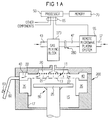
other layers. Fig. 1A is a vertical, cross-sectional view of one embodiment of a
CVD apparatus 10 according to a specific embodiment. In addition to being
capable of depositing dielectric layers, the apparatus according to the present
invention has high temperature heating capabilities useful for performing
reflow of deposited dielectric layers for planarization, or for driving in
dopants from a deposited doped dielectric layer when forming ultra-shallow
doped regions. Further, the apparatus can provide efficient cleaning of
various CVD chamber components and cleaning of wafer surfaces. CVD
apparatus 10 provides these multiple capabilities in situ in a single vacuum
chamber 15. Accordingly, multiple process steps may be performed in a single
chamber without having the wafer transferred out of that chamber into other
external chambers. This results in a lower moisture content on the wafers by
eliminating opportunities to absorb moisture from the ambient air and,
advantageously increases the dopant retention in the deposited dielectric
layer. In addition, performing multiple process steps in a single chamber
saves time, which increases the overall throughput of the process.
Referring to Fig. 1A, CVD apparatus 10 includes an enclosure
assembly 200 housing a vacuum chamber 15 with a gas reaction area 16. A
gas distribution plate 20 is provided above the gas reaction area 16 for
dispersing reactive gases through perforated holes in plate 20 to a wafer (not
shown) that rests on a vertically movable heater 25 (also referred to as a
wafer support pedestal or susceptor). CVD apparatus 10 further includes a
heater/lift assembly 30 for heating the wafer supported on heater 25.
Heater/lift assembly 30 also can be controllably moved between a lower
loading/off-loading position and an upper processing position indicated by
dotted line 13 which is closely adjacent to plate 20, as shown in Fig. 1A. A
center board (not shown) includes sensors for providing information on the
position of the wafer. As discussed in detail below, heater 25 includes
resistively-heated components enclosed in a ceramic, preferably aluminum
nitride. In an exemplary embodiment, all surfaces of heater 25 exposed to
vacuum chamber 15 are made of a ceramic material, such as aluminum oxide
(Al2O3 or alumina) or aluminum nitride. When heater 25 and the wafer are
in processing position 13, they are surrounded by a chamber liner 35 along
the inside walls 17 of apparatus 10 and by an annular pumping channel 40,
formed by chamber liner 35 and a top portion of chamber 15. As discussed in
detail below, the surface of chamber liner 35 preferably comprises a ceramic
material, such as alumina or aluminum nitride, which serves to lower the
temperature gradient between resistively-heated heater 25 (high
temperature) and chamber walls 17, which are at a much lower temperature
relative to heater 25.
Reactive and carrier gases are supplied through supply line 43
into a gas mixing box (or gas mixing block) 273 (Fig. 5), where they are
preferably mixed together and delivered to plate 20. Gas mixing box 273 is
preferably a dual input mixing block coupled to a process gas supply line 43
and to a cleaning gas conduit 47. As will be discussed in detail below, a
processor 50 preferably controllably operates a gate valve 280 (Fig. 5) to
choose which of these two alternate sources of gases are sent to plate 20 for
dispersing into chamber 15. Conduit 47 receives gases from an integral
remote microwave plasma system 55, which has an inlet 57 for receiving
input gases. During deposition processing, gas supplied to plate 20 is vented
toward the wafer surface (as indicated by arrows 21), where it may be
uniformly distributed radially across the wafer surface, typically in a laminar
flow. Purging gas may be delivered into chamber 15 from an inlet port or
tube (not shown) through the bottom wall of enclosure assembly 200. The
purging gas flows upward past heater 25 and to an annular pumping channel
40. An exhaust system then exhausts the gas (as indicated by arrows 22) into
the annular pumping channel 40 and through an exhaust line 60 by a
vacuum pump system (not shown). Exhaust gases and residues are
preferably released from annular pumping channel 40 through exhaust line
60 at a rate controlled by a throttle valve system 63.
In the representative embodiment, the chemical vapor
deposition process performed in CVD apparatus 10 is a thermal, sub-atmospheric
pressure process, often referred to as sub-atmospheric CVD
(SACVD). As discussed earlier, thermal CVD processes supply reactive gases
to the substrate surface where heat-induced chemical reactions
(homogeneous or heterogeneous) take place to produce a desired film. In
CVD apparatus 10, heat is distributed by resistively-heated heater 25, as
discussed in detail below, that is capable of reaching temperatures as high as
about 400-800°C. Such heat distribution provides uniform, rapid thermal
heating of the wafer for effecting deposition, reflow and/or drive-in, cleaning,
and/or seasoning/gettering steps in a multiple-step process in situ in chamber
15. Alternatively, a controlled plasma may be formed adjacent to the wafer by
RF energy applied to gas distribution plate 20 from an RF power supply (not
shown). In embodiments additionally having a lower RF electrode, the RF
power supply can supply either single frequency RF power to plate 20 or
mixed frequency RF power to plate 20 and the lower RF electrode to enhance
the decomposition of reactive species introduced into process chamber 15. In
a plasma process, some of the components of vapor deposition apparatus 10
would have to be modified to accommodate the RF energy, as discussed
below.
Remote microwave plasma system 55 integrally provided in
CVD apparatus 10 is preferably adapted for performing periodic cleaning of
undesired deposition residue from various components of chamber 15,
including walls 17 as well as other components. Further, remote microwave
plasma system 55 can also perform cleaning or etching of native oxides or
residues from the surface of the wafer, depending on the desired application.
Although gases input via line 57 into plasma system 55 are reactive cleaning
gases for creating a plasma to provide fluorine, chlorine, or other radicals,
remote microwave plasma system 55 also may be adapted to deposit plasma
enhanced CVD films by inputting deposition reactive gases into system 55 via
input line 57. Generally, remote microwave plasma system 55 receives gases
via input line 57, which are energized by microwave radiation to create a
plasma with etching radicals which are then sent via conduit 47 for
dispersion through plate 20 to chamber 15. Specific details of plasma system
55 will be discussed further below. Some embodiments of apparatus 10 may
also include a radio frequency (RF) plasma system to provide in situ plasma
capability.
Motors and optical sensors (not shown) are used to move and
determine the position of movable mechanical assemblies such as throttle
valve system 63 and heater 25. The heater/lift assembly 30, motors, gate
valve 280, throttle valve system 63, remote microwave plasma system 55, and
other system components are controlled by processor 50 over control lines
65, of which only some are shown.
Processor 50 controls all of the activities of the CVD machine.
Acting as the system controller, processor 50 executes system control
software, which is a computer program stored in a memory 70 coupled to
processor 50. Preferably, memory 70 may be a hard disk drive, but of course
memory 70 may be other kinds of memory. In addition to a hard disk drive
(e.g., memory 70), CVD apparatus 10 in a preferred embodiment includes a
floppy disk drive and a card rack. Processor 50 operates under the control of
the system control software, which includes sets of instructions that dictate
the timing, mixture of gases, chamber pressure, chamber temperature,
microwave power levels, susceptor position, and other parameters of a
particular process. Other computer programs such as those stored on other
memory including, for example, a floppy disk or other computer program
product inserted in a disk drive or other appropriate drive, may also be used
to operate processor 50. System control software will be discussed in detail
below. The card rack contains a single-board computer, analog and digital
input/output boards, interface boards and stepper motor controller boards.
Various parts of CVD apparatus 10 conform to the Versa Modular European
(VME) standard which defines board, card cage, and connector dimensions
and types. The VME standard also defines the bus structure having a 16-bit
data bus and 24-bit address bus.
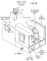
The interface between a user and processor 50 is via a CRT
monitor 73a and light pen 73b, shown in Fig. 1B which is a simplified
diagram of the system monitor and CVD apparatus 10, illustrated as one of
the chambers in a multichamber system. CVD apparatus 10 is preferably
attached to a mainframe unit 75 which contains and provides electrical,
plumbing and other support functions for the apparatus 10. Exemplary
mainframe units compatible with the illustrative embodiment of CVD
apparatus 10 are currently commercially available as the Precision 5000Ô
and the Centura 5200Ô systems from Applied Materials, Inc. of Santa Clara,
California. The multichamber system has the capability to transfer a wafer
between its chambers without breaking the vacuum and without having to
expose the wafer to moisture or other contaminants outside the
multichamber system. An advantage of the multichamber system is that
different chambers in the multichamber system may be used for different
purposes in the entire process. For example, one chamber may be used for
deposition of oxides, another may be used for rapid thermal processing, and
yet another may be used for oxide cleaning. The process may proceed
uninterrupted within the multichamber system, thereby preventing
contamination of wafers that often occurs when transferring wafers between
various separate individual chambers (not in a multichamber system) for
different parts of a process.
In the preferred embodiment two monitors 73a are used, one
mounted in the clean room wall for the operators and the other behind the
wall for the service technicians. Both monitors 73a simultaneously display
the same information, but only one light pen 73b is enabled. The light pen
73b detects light emitted by CRT display with a light sensor in the tip of the
pen. To select a particular screen or function, the operator touches a
designated area of the display screen and pushes the button on the pen 73b.
The touched area changes its highlighted color, or a new menu or screen is
displayed, confirming communication between the light pen and the display
screen. Of course, other devices, such as a keyboard, mouse, or other pointing
or communication device, may be used instead of or in addition to light pen
73b to allow the user to communicate with processor 50.
Fig. 1C illustrates a general overview of CVD apparatus 10 in
relation to a gas supply panel 80 located in a clean room. As discussed above,
CVD apparatus 10 includes chamber 15 with heater 25, gas mixing box 273
with inputs from supply line 43 and conduit 47, and remote microwave
plasma system 55 with input line 57. As mentioned above, gas mixing box
273 is for mixing and injecting deposition gas(es) and clean gas(es) or other
gas(es) through inlet tube 43 to the processing chamber 15. As seen in Fig.
1C, remote microwave plasma system 55 is integrally located and mounted
below chamber 15 with conduit 47 coming up alongside chamber 15 to gate
valve 280 and gas mixing box 273, located above chamber 15. Similarly, gas
supply line 43, which comes up alongside chamber 15 to gas mixing box 273,
is provided with reactive gases via lines 83 and 85 from gas supply panel 80.
Gas supply panel 80 includes lines to gas or liquid supply sources 90,
containing gases or liquids that may vary depending on the desired processes
used for a particular application. Gas supply panel 80 has a mixing system 93
which receives the deposition process and carrier gases (or vaporized liquids)
from sources 90 for mixing and sending to gas mixing box 273 via line 85 to
supply line 43. Generally, supply lines for each of the process gases include (i)
shut-off valves 95 that can be used to automatically or manually shut off the
flow of process gas into line 85 or line 57, and (ii) mass flow controllers 100
that measure the flow of gas or liquid through the supply lines. When toxic
gases (for example, ozone and the clean gas) are used in the process, the
several shut-off valves 95 may be positioned on each gas supply line in
conventional configurations. The rate at which the deposition and carrier
gases including, for example, tetraethylorthosilane (TEOS), helium (He), and
nitrogen (N2), and optionally triethylphosphate (TEPO), triethylborate
(TEB), and/or other dopant sources, are supplied to gas mixing system 93 is
also controlled by liquid or gas mass flow controllers (MFCs) (not shown)
and/or by valves (not shown). In some embodiments, gas mixing system 93
includes a liquid injection system for vaporizing reactant liquids such as
TEOS and TEPO. According to these embodiments, a mixture including
TEPO as the phosphorus source, TEOS as the silicon source, and one or
more gaseous oxygen sources, such as oxygen (O2) or ozone (O3), may be
formed with gas mixing system 93. The TEPO and TEOS are all liquid
sources that also may be vaporized by conventional boiler-type or bubbler-type
hot boxes in other embodiments. A liquid injection system is preferred
as it provides greater control of the volume of reactant liquid introduced into
the gas mixing system. The vaporized gases are then mixed in the gas mixing
system with a carrier gas, such as helium, before being delivered to heated
line 85. Of course, it is recognized that other sources of dopants, silicon, and
oxygen also may be used.
Additionally, gas supply panel 80 includes switching valve 95,
which under the control of processor 50, can selectively send the clean gas
with N2 along process gas line 83 to gas supply line 43 or along clean gas line
57 to remote microwave plasma system 55. When processor 50 causes
switching valve 95 to send the clean gas with N2 via input line 57 to plasma
system 55, a plasma remote from chamber 15 is formed due to application of
microwave energy and cleaning radicals are produced for transfer to gas
conduit 47. Processor 50 can also cause another valve 96 to send ozone
through line 83 to gas supply line 43 and to send the deposition and carrier
gases from gas mixing system 93 through heated line 85 to gas supply line 43.
In alternative embodiments, valve 95 is connected at its output only to line
97 and selectively allows clean gas and N2 to pass through line 97 to a
switching valve 105 (not shown). Located at a point close to inlet 57 and
remote system 55, switching valve 105 in these embodiments would be
connected to inlet 57 to remote microwave system 55 and also to line 83
leading to inlet 43. In specific embodiments, gate valve 280 may be controlled
by processor 50, with instructions from the system software computer
program, to select either the clean gases or the deposition gases to flow into
chamber 15.
Located remote from the clean room where chamber 15 of
apparatus 10 is located are a microwave power supply 110 and ozonator 115.
Power supply 110 provides power to the magnetron in remote plasma system
55. Ozonator 115, applies power to oxygen (O2) which is used as input to
provide ozone (O3) as output for use as at least one of the sources 90. In
other embodiments, power supply 110 and ozonator 115 may be located in
the clean room rather than being remotely located. Further, in multichamber
systems requiring multiple ozone sources and/or multiple remote microwave
plasma systems 55, multiple ozonators 115 and multiple power supplies 110
may be provided.
The processes for depositing the film, performing a clean, and
performing reflow or drive-in steps can be implemented using a computer
program product that is executed by processor 50. The computer program
code can be written in any conventional computer readable programming
language such as, for example, 68000 assembly language, C, C++, Pascal,
Fortran, or other language. Suitable program code is entered into a single
file, or multiple files, using a conventional text editor and is stored or
embodied in a computer-usable medium, such as a memory system of the
computer. If the entered code text is in a high-level language, the code is
compiled, and the resultant compiler code is then linked with an object code
of precompiled Windows library routines. To execute the linked compiled
object code, the system user invokes the object code, causing the computer
system to load the code in memory, from which the CPU reads and executes
the code to perform the tasks identified in the program.
Fig. 1D is an illustrative block diagram of the hierarchical
control structure of the system control software, computer program 150,
according to a specific embodiment. Using a light pen interface, a user enters
a process set number and process chamber number into a process selector
subroutine 153 in response to menus or screens displayed on the CRT
monitor. The process sets, which are predetermined sets of process
parameters necessary to carry out specified processes, are identified by
predefined set numbers. Process selector subroutine 153 identifies (i) the
desired process chamber, and (ii) the desired set of process parameters
needed to operate the process chamber for performing the desired process.
The process parameters for performing a specific process relate to process
conditions such as, for example, process gas composition and flow rates,
temperature, pressure, plasma conditions such as magnetron power levels
(and alternatively to or in addition to high- and low-frequency RF power
levels and the low-frequency RF frequency, for embodiments equipped with
RF plasma systems), cooling gas pressure, and chamber wall temperature.
Process selector subroutine 153 controls what type of process (deposition,
wafer cleaning, chamber cleaning, chamber gettering, reflowing) is
performed at a certain time in chamber 15. In some embodiments, there may
be more than one process selector subroutine. The process parameters are
provided to the user in the form of a recipe and may be entered utilizing the
light pen/CRT monitor interface.
The signals for monitoring the process are provided by the
analog input board and digital input board of the system controller, and the
signals for controlling the process are output on the analog output board and
digital output board of CVD system 10.
A process sequencer subroutine 155 comprises program code for
accepting the identified process chamber and set of process parameters from
process selector subroutine 153, and for controlling operation of the various
process chambers. Multiple users can enter process set numbers and process
chamber numbers, or a single user can enter multiple process set numbers
and process chamber numbers, so sequencer subroutine 155 operates to
schedule the selected processes in the desired sequence. Preferably,
sequencer subroutine 155 includes program code to perform the steps of (i)
monitoring the operation of the process chambers to determine if the
chambers are being used, (ii) determining what processes are being carried
out in the chambers being used, and (iii) executing the desired process based
on availability of a process chamber and the type of process to be carried out.
Conventional methods of monitoring the process chambers can be used, such
as polling. When scheduling which process is to be executed, sequencer
subroutine 155 can be designed to take into consideration the present
condition of the process chamber being used in comparison with the desired
process conditions for a selected process, or the "age" of each particular
user-entered request, or any other relevant factor a system programmer
desires to include for determining scheduling priorities.
Once sequencer subroutine 155 determines which process
chamber and process set combination is going to be executed next, the
sequencer subroutine 155 initiates execution of the process set by passing the
particular process set parameters to a chamber manager subroutine 157a-c
which controls multiple processing tasks in a process chamber 15 according
to the process set determined by sequencer subroutine 155. For example, the
chamber manager subroutine 157a comprises program code for controlling
CVD and cleaning process operations in process chamber 15. Chamber
manager subroutine 157 also controls execution of various chamber
component subroutines which control operation of the chamber components
necessary to carry out the selected process set. Examples of chamber
component subroutines are substrate positioning subroutine 160, process gas
control subroutine 163, pressure control subroutine 165, heater control
subroutine 167, plasma control subroutine 170, endpoint detect control
subroutine 159, and gettering control subroutine 169. Depending on the
specific configuration of the CVD chamber, some embodiments include all of
the above subroutines, while other embodiments may include only some of
the subroutines. Those having ordinary skill in the art would readily
recognize that other chamber control subroutines can be included depending
on what processes are to be performed in process chamber 15. In operation,
chamber manager subroutine 157a selectively schedules or calls the process
component subroutines in accordance with the particular process set being
executed. Chamber manager subroutine 157a schedules the process
component subroutines much like sequencer subroutine 155 schedules which
process chamber 15 and process set are to be executed next. Typically,
chamber manager subroutine 157a includes steps of monitoring the various
chamber components, determining which components need to be operated
based on the process parameters for the process set to be executed, and
initiating execution of a chamber component subroutine responsive to the
monitoring and determining steps.
Operation of particular chamber component subroutines will
now be described with reference to Fig. 1D. Substrate positioning subroutine
160 comprises program code for controlling chamber components that are
used to load the substrate onto heater 25 and, optionally, to lift the substrate
to a desired height in chamber 15 to control the spacing between the
substrate and gas distribution manifold 20. When a substrate is loaded into
process chamber 15, heater 25 is lowered to receive the substrate and then
heater 25 is raised to the desired height. In operation, substrate positioning
subroutine 160 controls movement of heater 25 in response to process set
parameters related to the support height that are transferred from chamber
manager subroutine 157a.
Process gas control subroutine 163 has program code for
controlling process gas composition and flow rates. Process gas control
subroutine 163 controls the open/close position of the safety shut-off valves,
and also ramps up/down the mass flow controllers to obtain the desired gas
flow rate. Process gas control subroutine 163 is invoked by the chamber
manager subroutine 157a, as are all chamber component subroutines, and
receives subroutine process parameters related to the desired gas flow rates
from the chamber manager. Typically, process gas control subroutine 163
operates by opening the gas supply lines and repeatedly (i) reading the
necessary mass flow controllers, (ii) comparing the readings to the desired
flow rates received from chamber manager subroutine 157a, and (iii)
adjusting the flow rates of the gas supply lines as necessary. Furthermore,
process gas control subroutine 163 includes steps for monitoring the gas flow
rates for unsafe rates, and activating the safety shut-off valves when an
unsafe condition is detected. Process gas control subroutine 163 also controls
the gas composition and flow rates for clean gases as well as for deposition
gases, depending on the desired process (clean or deposition or other) that is
selected. Alternative embodiments could have more than one process gas
control subroutine 613, each subroutine 613 controlling a specific type of
process or specific sets of gas lines.
In some processes, an inert gas such as nitrogen or argon is
flowed into chamber 15 to stabilize the pressure in the chamber before
reactive process gases are introduced. For these processes, process gas
control subroutine 163 is programmed to include steps for flowing the inert
gas into chamber 15 for an amount of time necessary to stabilize the pressure
in the chamber, and then the steps described above would be carried out.
Additionally, when a process gas is to be vaporized from a liquid precursor,
for example TEOS, process gas control subroutine 163 would be written to
include steps for bubbling a delivery gas such as helium through the liquid
precursor in a bubbler assembly, or introducing a carrier gas such as helium
to a liquid injection system. When a bubbler is used for this type of process,
process gas control subroutine 163 regulates the flow of the delivery gas, the
pressure in the bubbler, and the bubbler temperature in order to obtain the
desired process gas flow rates. As discussed above, the desired process gas
flow rates are transferred to process gas control subroutine 163 as process
parameters. Furthermore, process gas control subroutine 163 includes steps
for obtaining the necessary delivery gas flow rate, bubbler pressure, and
bubbler temperature for the desired process gas flow rate by accessing a
stored table containing the necessary values for a given process gas flow rate.
Once the necessary values are obtained, the delivery gas flow rate, bubbler
pressure and bubbler temperature are monitored, compared to the necessary
values and adjusted accordingly.
The pressure control subroutine 165 comprises program code
for controlling the pressure in the chamber 15 by regulating the aperture size
of the throttle valve in the exhaust system of the chamber. The aperture size
of the throttle valve is set to control the chamber pressure at a desired level
in relation to the total process gas flow, the size of the process chamber, and
the pumping set-point pressure for the exhaust system. When pressure
control subroutine 165 is invoked, the desired or target pressure level is
received as a parameter from chamber manager subroutine 157a. The
pressure control subroutine 165 measures the pressure in chamber 15 by
reading one or more conventional pressure nanometers connected to the
chamber, compares the measure value(s) to the target pressure, obtains PID
(proportional, integral, and differential) values corresponding to the target
pressure from a stored pressure table, and adjusts the throttle valve
according to the PID values obtained from the pressure table. Alternatively,
pressure control subroutine 165 can be written to open or close the throttle
valve to a particular aperture size to regulate the pressure in chamber 15 to
the desired level.
Heater control subroutine 167 comprises program code for
controlling the temperature of a heater element 473 used to resistively heat
heater 25 (and any substrate thereon). Referring to Fig. 1E, heater control
subroutine 167, which is also invoked by chamber manager subroutine 157a,
receives a desired target/set-point temperature parameter, Tdes, as an input
(step 580). In step 582, heater control subroutine 167 measures the current
temperature of heater 25 by measuring voltage output of a thermocouple
located in heater 25. The current temperature is denoted T(k), where k is the
current time step of heater control subroutine 167. The controller obtains
the temperature T(k) from the thermocouple voltage by looking up the
corresponding temperature in a stored conversion table or by calculating the
temperature using a fourth-order polynomial. In an exemplary embodiment,
heater control subroutine 167 in step 584 calculates the temperature error.
The temperature error, denoted Errtemp, is determined by the equation
Errtemp(k)=Tdes-T(k).
In step 584, heater control subroutine 167 will select one of two
control algorithms based on the absolute value of Errtemp(k). If the absolute
value of the temperature error is smaller than a predetermined boundary
error, the heater control subroutine will select a temperature regulator
algorithm (steps 586 and 588). This algorithm precisely controls the
temperature at the desired temperature, Tdes. If the absolute value of the
temperature error is greater than the boundary error, heater control
subroutine 167 will select a temperature ramp control algorithm (step 590).
This algorithm controls the rate at which the heater temperature will
approach the desired temperature, Tdes, i.e., it controls the rate at which the
temperature changes.
The temperature regulator algorithm (steps 586 and 588) uses
feedback and feedforward control to update the power delivered to the
heating element embedded in heater 25 so as to maintain the current
temperature, T(k), as close to Tdes as possible. The feedforward control in this
algorithm estimates the amount of power necessary to maintain the desired
temperature given the amount and type of gas flow and RF power supplied to
the chamber. The feedback control uses standard
Proportional-Integral-Derivative (PID) control terms to adjust the estimated
feedforward power based on the dynamic behavior of the temperature error,
Errtemp(k). PID control is the type of algorithm used in conventional heater
control systems without regard to the value of the temperature error. If these
routines seek to control the temperature ramp rate, they will define a
time-varying Tdes(k) and then employ the PID controller described above to
track this desired temperature trajectory.
In the present invention, heater control subroutine 167
preferably employs the temperature ramp control algorithm (steps 590) to
control power to heater 25 when the absolute value of temperature error is
greater than the boundary error. This algorithm controls T'(k), which is the
rate of change of the temperature, T(k), at time step k. The rate of change of
temperature should be controlled because the heater 25 can be made of a
ceramic material, which may fracture from thermal shock if the temperature
changes too quickly. The ramp control algorithm uses feedforward and
Proportional feedback control to control T'(k) to a predetermined desired
ramp rate function, T'des(T). The desired ramp rate is mainly a function of
the temperature of the heater and is based on the thermal shock resistance of
the heater 25 at various temperatures. Thus, the desired ramp rate may
continuously change based on the current measured temperature of the
heater, or it may be set at a constant based on a minimum rate that is low
enough to avoid thermal shock within the range of temperatures of a
particular process. The control algorithm also employs a saturation function
on the rate of change of power supplied to the heater to damp the system
response, which reduces oscillations in ramp rate.
Controllers that attempt to regulate ramp rate by tracking a
timed temperature trajectory at best can only guarantee that a desired
temperature, Tdes(K), will be achieved at some time K in the future. The
average ramp rate over the time interval of length K will be T'des. However,
the instantaneous rate of change of temperature T'(k) may vary widely
during that interval. Consider the case in which a disturbance causes the
temperature to remain stable for some interval of time less than K. The
controller will then attempt to as quickly as possible "catch up" to the desired
trajectory Tdes(k). The ramp rate for the time interval during which the
controller is catching up will be greater than T'des. That scenario could result
in thermal shock fracture. By controlling the ramp rate directly, the current
invention avoids this potential scenario.
Referring to Fig. 1E, an exemplary ramp control algorithm will
now be described. After the desired temperature, Tdes is input (step 580), the
current temperature T(k) is measured (step 582), and the temperature error
is determined (step 584), the ramp control algorithm calculates the actual
ramp rate T'(k) using a numerical differentiation technique. It also
determines the desired ramp rate, T'des(T(k)), based on the current value of
T(k), and the error in ramp rate, Errrrate=T'des(T(k))-T'(k) (steps 592 and
594). The actual ramp rate T'(k) is calculated from measured temperature
T(k) over a range of temperature measurement samples. In general,
T'des(T(k)) may be any continuous function of temperature in various
embodiments. In the specific embodiment, T'des(T(k)) is set to be a
predetermined constant value. The calculated ramp rate T'(k) is determined
by sampling (i.e., measuring) the temperature at a predetermined sample
rate (e.g., 10 times in a power update period, 1 second, in the specific
embodiment). Then, an average of the 10 samples is calculated and compared
to the average of the previous 10 samples. The difference between the
averages of the first 10 measured temperatures and the previous 10
measured temperatures is then divided by the power update period to obtain
an average measured temperature. The derivative of the average measured
temperature is then calculated to arrive at the calculated ramp rate T'(k).
The ramp rate error ErrRRate may then determined by taking the difference
between the constant-valued T'des(T(k)) and the calculated ramp rate T'(k) in
the specific embodiment (step 594). The above embodiment is an example of
one numerical differentiation technique that may be used, but other
techniques that may be more sophisticated also can be used in other
embodiments. In other embodiments, other sample rates also may be used.
To elaborate on step 596, an exemplary control function used in
the specific embodiment is given by the following equation:
P(k+1) = Pmodel[T(k),T'des(T(k))] + Kp*[T'des(T(k))-T'(k)]
where k is the current time step and k+1 is the next time step. P(k+1) is the
power that will be supplied to the heater at the next time step. Pmodel[T(k),
T'des(T(k))], which is a function of the desired ramp rate and measured
temperature, is some modeled approximation of the necessary power to give
a ramp rate of T'des(T(k)) at a temperature T(k). Kp is a control gain constant
(in Watts/(°C/second)) that is user-defined and multiplied with the ramp rate
error ErrRRate. In the specific embodiment, Pmodel[T(k),T'des(T(k))] can be
approximated as P(k). This approximation is particularly true for slow
systems such as the resistive heater with large thermal mass of the present
invention. The control function is then approximated by the following
equations:
P(k+1) = P(k) + Kp*[T'des(T(k))-T'(k)] P(k+1) - P(k) = Kp*[T'des(T(k))-T'(k)].
Because the response of the heater is slow, there is a lag
between the time power is adjusted and the time when the adjustment
produces the desired result. For example, if the temperature of the heater is
stable and the desired ramp rate is positive, the control will increase power
to the heater. The temperature will not, however, immediately rise according
to the desired ramp rate. The control will then at the next time step further
increase power. It will continue to increase power until the desired ramp rate
is met. By that time, however, the supplied power could be much greater
than that needed to maintain the desired ramp rate. The ramp rate will
continue to increase beyond its desired value. This is called overshoot. The
controller will react by reducing power, and slowly the ramp rate will
decrease. Once again, the controller can act faster than the heater, so it will
reduce power too much and the ramp rate will decrease beyond its desired
value. This is oscillation. Over time, the magnitude of the oscillations will
decrease and the ramp rate will reach a constant, steady-state value. Because
all real systems undergo small disturbances, there will also be a small steady-state
error.
The value of Kp determines the size of the overshoot and the
steady-state error. If Kp is large, the system will be more oscillatory, but
steady-state error will be small. If Kp is small, the opposite is true. Typically,
Kp can be large because Derivative control can be used to damp the system's
response, i.e. reduce overshoot and oscillation. Steady-state error can be
reduced by using Integral control, but this tends to increase overshoot and
oscillation and is preferably avoided in this control algorithm. In this case,
derivative control is not available. It would require numerically calculating
the second derivative of the temperature. Because the signal-to-noise ratio of
the thermocouple signal is low, its second derivative can not be calculated
reliably. Therefore, the present invention uses a large Kp to reduce
steady-state error and a saturation function (step 598) instead of derivative
control to dampen the system response. The saturation function effectively
schedules the gain Kp such that Kp is inversely proportional to the ramp rate
error, ErrRRate. During the transient portion of the system response, when
errors are larger and overshoot can occur, the effective gain is small. In
steady-state, errors are small, so the effective Kp is large.
The exemplary saturation function used to dampen system
response is given by the following equations (step 598). For these equations,
P(k+1) refers to the power defined by the control equation given above.
P
1(k+1) is the actual power supplied to the heater. P'
max is the predetermined
maximum allowable change in supplied power from one time step to the next.
The exemplary saturation function is as follows:
A new term Kpeff(k) can now be defined as the effective gain of
the controller at time step k. Clearly, if P1(k+1)=P(k+1) the effective gain at
time k equals the gain Kp. But if the saturation function is applied, Kpeff(k) is
defined by substituting P(k+1) for P1( k+1) in the equations above and
combining them with the equation: P(k+1) = Pmodel[T(k),T'des(T(k))] +
Kp*[T'des(T(k))-T'(k)]. The term Kpeff(k) is as follows:
P'max= Kpeff(k)*ErrRRate(k); Kpeff(k) =P'max/ErrRRate(k).
By making the effective gain small when the ramp rate error is large,
overshoot and oscillation in the response are minimized by this saturation
function. This reduces the likelihood of damage to the heater from poor ramp
rate control. Accordingly, the ramp control algorithm of heater control
subroutine 167 dampens the system's response when large ramp rate errors
occur, thereby resulting in more efficient temperature control.
A plasma control subroutine 170 comprises program code for
setting the magnetron power levels and mode (CW or pulsed). In alternative
embodiments having RF plasma systems, plasma control subroutine 170 also
could include program code for setting low- and high-frequency RF power
levels applied to the process electrodes in chamber 15, and for setting the
low-frequency RF frequency employed. Of course, some embodiments may
have one plasma control subroutine 170 used for microwave power levels and
another plasma control subroutine 170 used for RF power levels. Like the
previously described chamber component subroutines, plasma control
subroutine 170 is invoked by chamber manager subroutine 157a.
A plasma control subroutine 170 comprises program code for
setting and adjusting the magnetron power levels and mode (CW or pulsed).
In alternative embodiments having RF plasma systems, plasma control
subroutine 170 also could include program code for setting low- and
high-frequency RF power levels applied to the process electrodes in chamber
15, and for setting the low-frequency RF frequency employed. Of course,
some embodiments may have one plasma control subroutine 170 used for
microwave power levels and another plasma control subroutine 170 used for
RF power levels. Like the previously described chamber component
subroutines, plasma control subroutine 170 is invoked by chamber manager
subroutine 157a. In embodiments having gate valve 280, plasma control
subroutine 170 also includes program code for opening and closing of gate
valve 280 to coordinate with the setting/adjusting of microwave power levels.
Alternatively, the system software may have a separate gate valve control
subroutine in embodiments having gate valve 280.
An endpoint detect control subroutine 159 includes program
code for managing endpoint detection by controlling a light source and a light
detector, receiving data from the light detector for use in comparing light
intensity changes from absorbance, and optionally stopping the cleaning
process upon detecting a predetermined light intensity level or raising a flag
indicating the endpoint of the cleaning process. Endpoint detect control
subroutine 159 also may be invoked by chamber manager subroutine 157a.
Endpoint detect control subroutine 159 is included for those embodiments
using the endpoint detection system described below. It is recognized that
embodiments not having an endpoint detection system would not need to use
or have endpoint detect control subroutine 159.
Optionally, a gettering control subroutine 169 may be included
that can be invoked by chamber manager subroutine 157a. Gettering control
subroutine 169 includes program code for controlling gettering processes
that may be used for chamber seasoning, post-clean fluorine gettering, etc. In
some embodiments, gettering control subroutine 169 can invoke specified
software built into the clean recipe to facilitate gettering control in
combination with the clean recipe used.
The CVD system description presented above is mainly for
general illustrative purposes and should not be considered as limiting the
scope of the present invention. The exemplary CVD system 10 is a
single-wafer vacuum chamber system. However, other CVD systems that are
multiple-wafer chamber systems may be used in other embodiments of the
invention. It should be understood, however, that although certain features
of the invention are shown and described as part of a CVD chamber in a
multichamber processing system, the invention is not necessarily intended to
be limited in this manner. That is, the invention can be used in a variety of
processing chambers, such as etch chambers, diffusion chambers or the like.
Variations of the above described system such as variations in design, heater
design, location of RF power connections, software operation and structure,
specific algorithms used in some software subroutines, configuration of gas
inlet lines and valves, and other modifications are possible. Additionally,
other plasma CVD equipment such as electron cyclotron resonance (ECR)
plasma CVD devices, induction coupled RF high density plasma CVD devices,
or the like may be employed. The dielectric layers and methods for forming
such layers for use in the present invention should not necessarily be limited
to any specific apparatus or to any specific plasma excitation method.
As shown in Figs. 2 and 3, CVD apparatus 10 generally includes
an enclosure assembly 200 having vertically movable heater (wafer support
pedestal or susceptor) 25 for supporting a semiconductor wafer within a
vacuum chamber 15. Process gas(es) are delivered into chamber 15 to
perform various deposition and etching steps on the wafer. A gas distribution
system 205 (Figs. 2-6) distributes process gases from gas sources 90 (Fig. 1C)
onto the wafer, and an exhaust system 210 (Figs. 2-4) discharges the process
gases and other residue from chamber 15. CVD apparatus 10 further includes
a heater/lift assembly 30 (Figs. 1A, 9-15) that includes heater 25 for heating
the wafer and for lifting the wafer upwards into a processing position within
chamber 15. An integral remote microwave plasma system 55 (Figs. 1A and
16) is also provided in CVD apparatus 10 for periodic chamber cleaning,
wafer cleaning, or depositing steps.
As shown in Fig. 2, CVD apparatus 10 further includes a liquid
cooling system 215 for delivering coolant to various components of the
chamber 15 to cool these components during the high temperature
processing. Liquid cooling system 215 acts to decrease the temperature of
these chamber components to minimize undesired deposition onto these
components due to the high temperature processes. Liquid cooling system
215 includes a pair of water connections 217, 219 that supply cooling water
through the heater/lift assembly 30 and a coolant manifold (not shown) for
delivering coolant to the gas distribution system 205 (discussed below). A
waterflow detector 220 detects the waterflow from a heat exchanger (not
shown) to enclosure assembly 200. Preferred embodiments of the individual
systems of apparatus 10 will be described in further detail below.
A. Enclosure Assembly
Referring to Figs. 2 and 6, enclosure assembly 200 is preferably
an integral housing made from a process-compatible material, such as
aluminum or anodized aluminum. Enclosure assembly 200 includes an outer
lid assembly 225 for delivering process and clean gases through an inlet tube
43 to an inner lid assembly 230 within assembly 200. Inner lid assembly 230
functions to disperse the gases throughout chamber 15 onto a wafer (not
shown) supported on heater 25. As shown in Fig. 2, a lid cover 233 provides
access to the components on the top of enclosure assembly 200 (i.e., outer lid
assembly 32), and shields the operator from exposure to high temperatures
during system operation. For SACVD processes, lid cover 233 preferably
includes a cutout 235 to allow clearance for lid clamps 237 that ensure gas
integrity of the chamber 16. Lid cover 233 generally remains closed during
most process steps unless the chamber is opened, for example, to perform a
preventive maintenance chamber cleaning, thereby breaking the vacuum and
bringing the chamber to atmospheric pressure. A lid hinge 239 includes a
locking ratchet mechanism 241 to prevent the lid cover 233 from falling
closed.
As shown in Fig. 2, enclosure assembly 200 defines a vacuum
lock door (not shown) and a slit valve opening 243 through which a wafer
loading assembly (not shown) transports a wafer W into process chamber 16
and loads wafer W onto heater 25. The wafer loading assembly is preferably a
conventional robotic mechanism disposed within a transfer chamber (not
shown) of the multichamber processing system. A suitable robotic transfer
assembly is described in commonly assigned U.S. Patent No. 4,951,601 to
Maydan, the complete disclosure of which is incorporated herein by
reference.
Referring to Figs. 3, 4, 7A and 7B, the inside wall 245 of
enclosure assembly 200 around chamber 15 is covered with a chamber liner
250, which rests on a shelf 252 of enclosure assembly 200. Chamber liner 250
serves to inhibit process gases from flowing to the back side of the wafer. In
addition, since heater 25 has a smaller diameter than enclosure assembly
200, liner 250 inhibits the flow of process gases below heater 25 to the lower
portion of chamber 15. Accordingly, undesired deposition onto the bottom of
heater 25 and the lower portion of chamber 15 is minimized. Further, liner
250 provides thermal insulation between the aluminum walls of enclosure
assembly 200 and the edge of the wafer on heater 25, in order to prevent
wafer edge cooling during high temperature processing. During high
temperature processing, liner 250 prevents excessive heat loss from the
hotter edges of the wafer on heater 25 (e.g., about 550-600°C) to the cooler
surrounding chamber walls (e.g., about 60°C). Without liner 250, the heat
effects at the edge of the wafer may adversely affect temperature uniformity
across the wafer and lead to non-uniform deposition. Liner 250 preferably
comprises an inner portion 253 formed of a process-compatible material that
is well suited for high temperature processes (e.g., greater than about 500°C).
Preferably, inner portion 253 of liner 250 comprises a ceramic material, such
as aluminum nitride, alumina, or the like, with alumina being the preferred
material. Inner portion 253 will usually have a thickness of about 0.1 to 1
inch (2,52 mm) and preferably about 0.2 to 0.3 inch (5 to 7,5 mm).
Liner 250 preferably comprises an outer portion 255 that
comprises a material that is less susceptible to cracking than ceramic, such as
aluminum. Outer portion 255 rests on shelf 252 of enclosure assembly, and
includes an annular lip 254 for supporting inner portion 253 of liner 250. In
a particularly preferred embodiment, outer portion 255 includes a plurality
of circumferentially spaced vertical struts 257 that define inner air gaps 259
therebetween, as shown in Figs. 7A and 7B. Air gaps 259 facilitate insulation
of the inner portion 253 of liner 250 from the outer chamber walls to
increase wafer temperature uniformity (otherwise the outer edge of the
wafer could cool down due to the surrounding chamber wall temperature,
which is cool relative to the heater and wafer temperature). In addition, air
gaps 259 provide thickness to liner 250 so that it can bridge the gap between
the outer chamber walls and heater 25 while minimizing the cracking or
other thermal damage that may occur with a thicker liner 250. Outer portion
255 of liner 250 usually has a thickness of about 0.5 to 2 inches (1,26 to 5 cm)
with an air gap 259 thickness of about 0.2 to 1.5 inches (0,5 to 3,78 cm), and
preferably about 0.9 to 1.1 inch (2,27 to 2,677 cm) with an air gap 259
thickness of about 0.6 to 0.9 inch (1,5 to 2,27 cm). An annular cover 261 is
positioned on the upper surface of outer liner 255 to form the lower wall of a
pumping channel 40 (discussed below). Annular cover 262 preferably
comprises a ceramic material, such as aluminum oxide or aluminum nitride,
to shield the aluminum outer portion 255 of liner 250 from process gases and
the heat within pumping channel 40.
In an alternative embodiment (not shown), liner 250 only
comprises inner ceramic portion 255 resting on shelf 252 of enclosure
assembly and annular cover 261 forming the bottom of pumping channel 40.
In this embodiment, outer portion 255 is replaced with an air gap (not
shown) between ceramic portion 255 and the inside wall of enclosure
assembly. The air gap insulates the high temperature wafer from the cooler
walls of the enclosure assembly, and it provides thickness to liner 250 to
bridge the gap between the chamber walls and heater 25.
B. Gas Distribution System
Referring to Figs. 2 and 6, outer lid assembly 225 generally
includes a lid or base plate 265, a coolant manifold (not shown), a clean gas
manifold 270 that includes conduit 47, gas mixing box 273 for mixing and
injecting process gas(es) and cleaning gas(es) through inlet tube 43 to the
processing chamber 15, and a gate valve 280 for selectively distributing
cleaning and/or process gases to gas mixing box 273. Of course, it should be
clearly understood that gate valve 280 is optional, and that outer lid
assembly 225 can be modified to selectively distribute cleaning and/or
process gases to box 273 without a gate valve. As shown in Fig. 4, gas mixing
box 273, clean gas manifold 277 and gate valve 280 are preferably fastened,
e.g., bolted, to the top surface of base plate 265. First and second gas
passages 83, 85 are mounted to the exterior of plate 265, and extend into gas
mixing box 273. Gas passages 83, 85 each have inlets suitably coupled to
sources 90 of gas (see Fig. 1C), such as ozone, TEOS, TEPO, helium,
nitrogen, clean gas, or the like, and outlets (not shown) in communication
with a mixing area 93 within box 273 for mixing the gases prior to delivering
them through inlet tube 43 into the inner lid assembly 230.
It should be noted that for plasma processes, CVD apparatus 10
will further include a gas feed-through box (not shown) housing gas passages
83, 85 to enable the application of high voltage RF power to the gas box
without gas breakdown, and without gas deposition in the gas distribution
system. A description of an exemplary gas feed-through box can be found in
U.S. Patent No. 4,872,947 to Wang, the complete disclosure of which is
incorporated herein by reference.
As shown in Fig. 6A, clean gas manifold 70 includes conduit 47
for receiving gas(es) from inlet 290, and directing these gas(es) through a
fluid passage 293 into gas mixing box 273. Gate valve 280 includes a valve
plug (not shown) seated within passage 293 for selectively allowing or
preventing the gases from passing through conduit 47 into gas mixing box
273. Gate valve 280 may be manually operated by actuating handle 281, or
gate valve 280 may be controlled by processor 50. During cleaning (discussed
below), gate valve 280 is configured to allow the clean gases from plasma
system 55 to pass into box 273, where they are directed through inlet tube 43
into chamber 15 to etch the wafer or the inner chamber walls and the other
components of apparatus 10.
As shown in Fig. 3, clean gas manifold 270 is constructed
integral to the top part of enclosure assembly 200 of apparatus 10, with
conduit 47 having an appropriate bend or curve from the top toward the side
of chamber 15. Conduit 47 of manifold 270 has an opening into a passage
integrally formed within a side wall of enclosure assembly 200 of apparatus
10, which may become heated due to the high temperatures at which heater
25 operates. This passage is equipped with an internal liner 291 that serves
to protect the inner surfaces of the passage in enclosure assembly 200 from
corrosion and etching from the clean gas radicals entering from an applicator
tube 292. Liner 291 also prevents recombination of radicals in the clean gas.
Clean gases are introduced into applicator tube 292 from an inlet 57.
Radicals are created from clean gases in applicator tube 292 by microwave
energy radiated from a magnetron in plasma system 55, which is
advantageously located toward the bottom of chamber 15 in enclosure
assembly 200. The location of system 55 at the bottom of apparatus 10
facilitates servicing of chamber 15 for preventive maintenance cleanings,
repairs, etc. In particular, opening the lid of apparatus 10 in order to perform
preventive maintenance cleanings is easily done, since the bottom-mounted
remote microwave plasma system 55 is not located on top of the lid of
apparatus 10. Microwave plasma system 55 is discussed in further detail
below. As shown in Figs. 3 and 4, inlet tube 43 preferably includes an inner
passage 295 for delivering process gases into chamber 15, and an outer,
annular passage 297 in communication with passage 293 for directing
cleaning gases into the chamber.
The coolant manifold, which may be fastened to the top or side
surface of base plate 265, receives coolant fluid, such as water or a
glycol\water mixture, from the heat exchanger. The coolant is distributed
from the coolant manifold through an annular coolant channel 93 (Figs. 4
and 5) in base plate 265 to convectively and conductively remove heat from
plate 265 and the components of inner lid assembly 230 during processing
(discussed in further detail below).
As shown in Figs. 2 and 5, inner lid assembly 230 generally
includes base plate 265, a blocker or gas dispersion plate 301 and a
showerhead or gas distribution plate 20 for dispersing process and clean
gases into chamber 15. Plates 301, 20 are preferably formed from a process-compatible
material that is capable of withstanding high temperature
processes. For example, plates 301, 20 may comprise a ceramic material such
as aluminum oxide or aluminum nitride (AlN), or a metal, such as aluminum
or anodized aluminum. Preferably, the plates 301, 20 comprise a metal, such
as aluminum or anodized aluminum, to minimize gas deposition on the
surfaces of plates 301, 20. In a particularly preferred embodiment, gas
dispersion plate 301 comprises anodized aluminum and gas distribution plate
20 comprises aluminum. Gas distribution and gas dispersion plates 301, 20
are each directly fastened to a lower surface of base plate 265. Preferably, gas
distribution and dispersion plates 20, 301 are affixed to lower surface of base
plate 265 with a plurality of threaded mounting screws 303, 305,
respectively. Mounting screws 303, 305 provide a relatively tight, surface-to-surface
contact between contact surfaces of gas distribution and dispersion
plates 20, 301, respectively, and lower surface of base plate 265 to facilitate
conductive heat exchange therebetween (discussed in greater detail below).
The mounting screws 303, 305 comprise a process-compatible material, such
an nickel, HasteloyÔ, HaynesÔ or the like.
Referring to Figs. 4 and 5, gas distribution plate 20 is a
substantially flat plate 311 having an outer flange 313 with a plurality of
holes 315 for receiving mounting screws 305 to provide engagement of the
contact surface of plate 20 with lower surface of base plate 265. Base plate
265 includes an outer annular stand-off 316 that spaces gas distribution plate
20 from the bottom surface of 265 and forms a chamber 317 (see Fig. 4)
between these two plates for dispersing the process gas uniformly through a
plurality of gas distribution holes 315 onto a semiconductor wafer.
Alternatively, gas distribution plate 20 may comprise a dish-shaped device
(not shown) having a centrally disposed cavity defined by a side wall and a
base wall.
The size and arrangement of gas distribution holes 315 will
vary depending on the process characteristics. For example, the holes 315
may be uniformly spaced to provide a uniform distribution of gases onto the
wafer. On the other hand, holes 315 may be non-uniformly spaced and
arranged, if desired. Holes 315 will usually have a diameter in the range of
about 5-100 mil (0,126 to 2,5 mm) and preferably in the range of about 10-50
mil (0,252 to 1,26 mm). Preferably, gas distribution holes 315 are designed to
promote uniformity of deposition on the semiconductor wafer. The holes (as
well as the manifold temperature, discussed above) are also designed to avoid
the formation of deposits on the manifold outer (bottom) surface and, in
particular, to prevent the deposition of soft deposits on that surface which
could flake off and drop onto the wafer during and after processing. In an
exemplary embodiment, the hole array is one of generally concentric rings of
holes 315. The distances between adjacent rings (ring-to-ring spacings) are
approximately equal, and the hole-to-hole spacing within each ring is
approximately equal. A more complete description of a suitable arrangement
for the gas distribution holes is described in commonly assigned U.S. Patent
No. 4,872,947 to Wang, the complete disclosure of which has previously been
incorporated by reference.
Gas dispersion plate 301 is a generally circular disk 321
including a plurality of gas dispersion holes 325 for dispersing the gas
therethrough into the chamber 317 formed between outer stand-off 316 and
gas distribution plate 20. Base plate 265 preferably includes a second, inner
stand-off 318 for spacing dispersion plate 301 from base plate 265 and for
allowing gas passing through base plate 265 to disperse into a chamber 320
(see Fig. 4) formed between stand-off 318 and plate 301. Alternatively, gas
dispersion plate 301 may define a recess (not shown) for forming chamber
320 rather than stand-off 318. Dispersion holes 325 will usually have a
diameter of about 0.02 - 0.04 mm. Of course, it will be recognized by those
skilled in the art that dispersion plate 301 may be included in preferred
embodiments of the invention. However, the process gases may be passed
directly from base plate 265 into chamber 317 of gas distribution plate 20, in
other embodiments.
As shown in Figs. 4 and 5, base plate 265 is an integral, single-piece
element that functions to deliver process gas(es) to gas dispersion plate
301 and to mount the entire inner lid assembly 230 to the mainframe unit of
the processing chamber. In RF plasma processes, inner lid assembly 230 will
also include an isolator (not shown) that electrically insulates the chamber
lid from ground and isolates the chamber body from the RF gas box (not
shown). An exemplary lid assembly for use with RF plasma processes is
described in U.S. Patent No. 4,872,947 to Wang, the disclosure of which has
previously been incorporated by reference.
As shown in Fig. 8, base plate 265 has a lower surface 321 that
defines an annular pumping channel 40 for exhausting the deposition gases
(discussed in detail below). As shown in Figs. 4 and 5, base plate 265 defines
a central hole 327 in communication with inlet tube 43 for receiving the
mixed process gases from gas mixing box 273. Hole 327 is also in
communication with recess 311 of gas dispersion plate 301 for dispersing the
gas across plate 301 to holes 315. Base plate 265 further defines a coolant
passage 93 having an inlet 331 and an outlet 333 coupled to the cooling
system 215 for directing coolant fluid through portions of plate 215 to
convectively cool these portions of plate 265. Preferably, coolant passage 93
is formed within portions of base plate 265 that are relatively close to
mounting screws 303, 305. This facilitates conductive cooling through
contact surfaces of dispersion and distribution plates 301, 20 and lower
surface 326 of base plate 265. A more complete description of exemplary
designs for coolant passage 93 can be found in commonly assigned, co-pending
application Serial No. 08/631,902, filed April 16, 1996 (Attorney
Docket No. 1034), the complete disclosure of which is incorporated herein by
reference, and in commonly assigned U.S. Patent No. 4,872,947 to Wang, the
complete disclosure of which has previously been incorporated by reference.
Referring to Fig. 5, base plate 265 further defines an annular
recess 343 surrounding central hole 327 and an annular cap 345 disposed
within recess 343 fastened to base plate 265 above coolant passage 93.
Preferably, annular cap 345 is welded to upper surface of base plate 265 to
provide a tight seal over passage 93, thereby effectively preventing coolant
leakage from passage 93. With this configuration, passage 93 is formed
relatively close to gas distribution and dispersion plates 20, 301. In addition,
passage 93 is fabricated by forming a groove in the upper surface of base
plate 265, thereby decreasing the cost and complexity of manufacturing
plate.
Referring now to Figs. 6B and 6C, an alternative embodiment of
inner lid assembly 230' will now be described. Similar to the previous
embodiment, lid assembly 230' includes a base plate 265, a gas dispersion
plate 301 and a gas distribution plate 20 for dispersing process and clean
gases into chamber 15. In addition, base plate 265 includes an annular
coolant channel 500 for receiving a coolant liquid, such as water, to cool base
plate 265 and the other components of lid assembly 230'. In this embodiment,
base plate 265 further includes an additional annular fluid channel 502
extending around central hole 295 above gas dispersion plate 301 for
exchanging heat with the portion of base plate 265 immediately above gas
dispersion and gas distribution holes 325, 315.
Inner lid assembly 230' includes a plurality of bypass passages
510 extending from chamber 320 between base plate 265 and gas dispersion
plate 301 to vacuum chamber 15. Bypass passages 510 offer a lower
resistance to fluid flow than gas dispersion and gas distribution holes 325,
315. Accordingly, a large portion of the gas flowing into chamber 320 will
pass through bypass passages 520 directly into the vacuum chamber 15. In
an exemplary embodiment,, bypass passages 510 are preferably spaced
circumferentially around base plate 265 to uniformly deliver gases into the
chamber 15 (see Fig. 6E). In a preferred use of this embodiment, cleaning
gases, such as NF3, pass into chamber 320 and through gas dispersion and
gas distribution holes 325, 315, respectively. In addition, a portion of the
cleaning gases pass through bypass passages 510 directly into chamber 15 to
facilitate the delivery of the cleaning gases into chamber 15.
In this embodiment, vapor deposition apparatus 10 will
preferably include a control system, such as a valve coupled to a controller
(not shown) for preventing (or at least inhibiting) gases from passing
through bypass passages 510. For example, during processing, it is typically
desired that the process gases pass through gas distribution and dispersion
holes 325, 315 to uniformly disperse onto the wafer. Thus, the valve will be
closed to prevent the process gases from passing through bypass passages
510. When the chamber is cleaned, the valve will be opened to quickly deliver
at least a portion of the cleaning gases into the chamber. This increases the
speed and efficiency of the cleaning process, which reduces the down time of
apparatus 10. Of course, it will be recognized that process gases may also be
delivered through bypass passages 510, if desired.
C. The Exhaust System
Referring to Figs. 2-4, a pump (not shown) disposed exterior to
CVD apparatus 10 provides vacuum pressure to draw both the process and
purge gases, as well as residues, out of chamber 15 and through annular
pumping channel 40, where they are discharged from apparatus 10 along a
discharge conduit 60. As shown in Fig. 8, the deposition and clean gases are
exhausted radially outward over the wafer W (shown by arrows 351) through
an annular slot-shaped orifice 355 surrounding the chamber 15 and into
pumping channel 40. The annular slot-shaped orifice 355 and channel 40 are
preferably defined by the gap between the top of the chamber's cylindrical
side wall 17 (including inner portion 253 of the chamber liner 250, see Figs. 3
and 4) and the bottom of base plate 265. From the pumping channel 40, the
gases flow circumferentially around channel 40 (shown by arrows 357) and
through a downwardly extending gas passage 361, past a vacuum shut off
valve 363 (whose body is preferably integrated with the lower chamber body),
and into discharge conduit 60 which connects to an external vacuum pump
(not shown).
Alternatively, CVD apparatus 10 may include a separate
pumping plate (not shown) having a plurality of gas holes that directly
communicate process chamber 15 with pumping channel 40. In this
embodiment, the gas holes are circumferentially spaced around the central
opening of the chamber to facilitate the uniform discharge of process gas
through the holes. To accommodate the relative positions of inlets and
outlets, gas holes may extend in a radially outward direction from inlets to
outlets relative to central opening. This radial orientation of holes also
contributes to a substantially uniform discharge of the process and purge
gases and exhausted residues from the processing chamber 15. A more
complete description of this type of pumping plate can be found in commonly
assigned co-pending application Serial No. 08/606,880, filed February 26,
1996 (Attorney Docket No. 978), the complete disclosure of which is
incorporated herein by reference.
Referring to Figs. 2 and 3, a valve assembly (throttle valve
system) 369 includes an isolation valve 371 and a throttle valve 373 disposed
along discharge line 60 for controlling the flow rate of the gases through
pumping channel 40. The pressure within processing chamber 15 is
monitored with capacitance manometers 381, 383 (see Fig. 2) and controlled
by varying the flow cross-sectional area of conduit 60 with throttle valve 373.
Preferably, processor 50 receives from manometers 381, 383 signals that
indicate the chamber pressure. Processor 50 compares the measured
pressure value with set-point pressure values entered by operators (not
shown), and determines the necessary adjustment of throttle valve 333 that
is required to maintain the desired pressure within chamber 15. Processor 50
relays an adjustment signal through a controller 385 to a drive motor (not
shown), which adjusts throttle valve 373 to a proper setting corresponding to
the set-point pressure value. Suitable throttle valves for use with the present
invention are described in commonly assigned, co-pending application Serial
No. 08/672,891 entitled "Improved Apparatus and Methods for Controlling
Process Chamber Pressure" (Attorney Docket Nos. 891/DCVD-II/MBE), filed
June 28, 1996, the complete disclosure of which is incorporated herein by
reference.
Isolation valve 371 may be used to isolate process chamber 15
from the vacuum pump to minimize the reduction of chamber pressure due
to the pumping action of the pump. Isolation valve 371, together with
throttle valve 373, may also be used to calibrate the mass flow controllers
(not shown) of CVD apparatus 10. In some processes, liquid dopants are
vaporized, and then delivered into process chamber 15 along with a carrier
gas. The mass flow controllers are used to monitor the flow rate of the gas or
liquid dopants into the chamber 15. During calibration of the MFCs, isolation
valve 371 restricts or limits the gas flow to throttle valve 373 to maximize the
pressure increase in chamber 15, which facilitates MFC calibration.
D. Heater/Lift Assembly
Referring to Figs. 9-15, heater/lift assembly 30 will now be
described in detail. The heater/lift assembly 30 functions to lift the wafer into
the processing position within vacuum chamber 15 and to heat the wafer
during processing. At the outset, it should be noted that heater/lift assembly
30 may be modified for use, or directly placed into, a variety of processing
chambers other than the exemplary SACVD chamber described and shown
herein. For example, heater/lift assembly 40 may be used in a similar CVD
chamber that generates plasma with RF or microwave power, a metal CVD
(MCVD) chamber, or other conventional or non-conventional semiconductor
processing chambers.
Referring to Figs. 9 and 13, heater/lift assembly 30 generally
includes a resistively-heated wafer support pedestal or heater 25 attached to
upper and lower support shafts 391, 393, a lift tube 395 circumscribing
support shafts 391, 393 underneath heater 25 and a drive assembly 400 for
vertically moving the heater 25, shafts 200, 201 and lift tube 202 within
chamber 15. As discussed in detail below, heater 25 (and the wafer supported
thereon) can be controllably moved between a lower loading/unloading
position where they are substantially aligned with slot 243 in enclosure
assembly 200 and an upper processing position beneath gas distribution plate
20 (Figs. 3 and 4). As shown in Fig. 7, heater 25 includes an upper wafer
support surface 403 surrounded by an annular raised perimeter flange 405 so
that the wafer is accurately located during processing. Wafer support surface
403 has a diameter approximately equal to the diameter of wafer W at the
deposition temperature, e.g., at a temperature ranging from about 200-800°C.
This diameter will typically be about 6-8 inches (about 15 to 20 cm)
for large size wafers and about 3-5 inches (about 0,75 to 13,0 cm) for small
size wafers. Of course, other wafer sizes such as those with about 12 inch
(about 30 cm) diameters would be within the scope of the invention with
appropriate modification of the chamber, the chamber lining 250, and
support heater 25.
Support heater 25 preferably comprises a disk made from a
process-compatible material that is capable of withstanding relatively high
processing temperatures, i.e., up to 600-800°C or higher. The material should
also be resistant to deposition from the reactive chemistries associated with
the high temperature deposition, as well as resistant to etching by the
radicals in the clean gas. Suitable materials for heater 25 are ceramics, such
as aluminum nitride, aluminum oxide or the like. Aluminum nitride ceramic
is the preferred material for the heater 25 because it has high thermal
conductivity, excellent corrosion resistance, and excellent tolerance of
thermal shock. Thus, in a particularly preferred embodiment, the entire
outer surface of heater 25 comprises aluminum nitride. Aluminum nitride
has high temperature capabilities and high resistance to fluorine and ozone
chemistries used in chamber 15. Use of aluminum nitride, as compared to
stainless steel or aluminum materials, for heater 25 also has less backside
metal contamination in the processed wafer, resulting in more reliable
devices. In addition, aluminum tends to react with the fluorine containing
compounds typically used in cleaning gases to form a layer of an aluminum
fluoride compound that may eventually build-up and flake off into the
chamber or onto the wafer, resulting in contamination (discussed in further
detail below). Constructing the heater 25 of aluminum nitride effectively
eliminates this problematic reaction during cleaning.
Referring again to Fig. 7, drive assembly 400 may include a
variety of driving mechanisms, including a pneumatic cylinder, controllable
motor or the like. Preferably, a stepper motor 407 coupled to the heater via a
suitable gear drive 409 operates to vertically drive heater 25, shafts 391, 393
and lift tube 395 in controlled increments between the loading/unloading and
processing positions. Drive assembly 400 also includes upper and lower
bellows 411, 413 attached between the end of shaft 391 and the bottom of the
processing chamber to allow for substantially free vertical movement of
heater 25. In addition, bellows 411, 413 allow some angular movement to
ensure that the gas distribution faceplate 20 and the heater 25 are
substantially parallel during processing.
Referring to Figs. 4, 9 and 13, lift tube 395 surrounds the lower
portion of upper shaft 391 and assists in insulating upper bellows 411 from
thermal energy radiating from shaft 391, heater 25 and the inside of
processing chamber 15. Lift tube 395 usually comprises an aluminum shaft
418, an annular strike plate 420 resting on the upper surface of shaft 418 and
an annular flange 422 that mounts plate 420 to shaft 418. Flange 422 and
strike plate 420 are preferably formed from a material capable of
withstanding high temperatures, such as aluminum nitride or aluminum
oxide (Al2O3 in its ceramic or alumina form). Flange 422 and strike plate 420
insulate the aluminum shaft 418 from the heater to minimize warping or
fusing of shaft 418 to heater shaft 391 or to the process chamber. In an
exemplary embodiment, lift tube 395 includes a spring (not shown), such as a
wave spring, loaded between flange 422 and strike plate 420 to prevent or at
least inhibit rattling of the strike plate 420.
As shown in Figs. 4 and 13, a plurality of wafer-support/lift
fingers 430, usually at least two and preferably four, are slidably mounted
within guide studs 432 spaced about the periphery of heater 25. Fingers 430
extend downward below heater 25 so that strike plate 420 may engage
fingers 430 and lift them above the upper surface of heater 25 for loading and
unloading wafers. Lift fingers 430 are preferably made of a ceramic material,
such as aluminum oxide, and generally have a double truncated cone shaped
head (not shown) The four lift finger guide studs 432 are preferably not
uniformly distributed about the heater 25, but instead form a rectangle
having at least one side that is wider than the width of the robot blade, which
is typically a thin, flat bar (not shown), around which the lift fingers 430
must lift the wafer. The bottom end of the lift fingers 430 are rounded. The
fingers 430 have a relatively thick diameter of about 100-200 mil (2,52 to
5,04 mm), preferably about 150 mil (3,8 mm), and a relatively short length of
about 1-3 inches (2,52 to 7,56 cm), preferably 2 inches (5 cm), to minimize
finger binding to the heater during processing.
In use, the robot blade (not shown) transfers the wafer to the
chamber 15 when the heater 25 is in position opposite slit 243 (or actually
just below slit 243). The wafer is supported initially by lift fingers 430, which
are lifted above heater 25 with strike plate 420. As lift fingers 430 rise along
with heater 25, they encounter a stop (not shown). As heater 25 continues to
rise to the processing position opposite gas distribution faceplate 20, lift
fingers 430 sink into guide studs 432 within heater 25 and the wafer is
deposited onto wafer support surface 403 within annular flange 405. To
remove the wafer from chamber 15, the above steps are performed in reverse.
Referring again to Fig. 9, a resistive heater coil assembly 440 is
housed within heater 25 for transferring heat to the wafer during processing.
Upper and lower support shafts 391, 393 support the heater 25 and house
the necessary electrical connections to the heater coil assembly 440 within a
hollow core 445 (discussed below). Upper support shaft 391 is made of a
ceramic material capable of withstanding relatively high processing
temperatures. Preferably, shaft 391 will be fabricated from diffusion-bonded
aluminum nitride, which prevents deposition onto, as well as attack by
chemistries used in chamber 15 of, the electrodes and electrical connections
within shaft 391 that might otherwise occur if the aluminum nitride were
not present. Shaft 391 is preferably diffusion-bonded to heater 25 to provide
a gas-tight seal between heater 25 and shaft 391 such that the hollow core
445 of shaft 391 is at ambient temperature and pressure (preferably
atmospheric pressure, i.e., 760 Torr (1 x 10⁵ Pa) or 1 atm). In other
embodiments, hollow core 445 may be at a pressure of about 0.8-1.2 atm and
a temperature of about 10-200°C, while chamber 15 may be at temperatures
of at least about 400°C and pressures of about 20 mTorr (2,66 Pa) to about
600 Torr (8 x 10⁴ Pa) This configuration helps to protect the electrodes and
other electrical connections from corrosion from the process and clean gases
within chamber 15. In addition, maintaining the hollow core 445 of shaft 391
at ambient pressure minimizes arcing from the RF power source through
hollow core 445 to power leads or the aluminum shaft. This arcing that might
otherwise occur in a vacuum is thus avoided.
Referring to Figs. 9 and 10, upper support shaft 391 extends
through an opening 453 in the lower surface of enclosure assembly 200, and
is coupled to a base 455 that provides a gas seal between shaft 391 and
chamber 15. Upper support shaft 391 is fastened, e.g., bolted, to lower
support shaft 393, which comprises a suitable process-compatible material,
such as aluminum or an aluminum alloy. Lower support shaft 393 is
preferably a water-cooled aluminum shaft. However, lower support shaft 393
may also comprise a ceramic material, such as aluminum oxide or aluminum
nitride. One or more sealing members 457, e.g., O-rings, are positioned
between shafts 391, 393 to maintain the gas seal between core 445 and
chamber 15. As shown in Fig. 9, lower support shaft 393 is mounted to a
vertically movable support 461 on drive assembly 400 for moving the shafts
391, 393 and heater 25 between the loading and processing positions. Shaft
393 defines an inner coolant channel 463 passing around the electrical
connections to further insulate these connections from the high temperature
of the shaft. Coolant channel 463 has an inlet 464 and an outlet 466 coupled
to water connections 217, 219, respectively, of liquid cooling system 215.
Coolant channel 463 serves to maintain a relatively low temperature in the
lower chamber area to protect sealing member(s) 457. In an alternative
embodiment, heater assembly 30 comprises a single shaft (not shown) that
supports heater 25 and extends through the lower opening 453 in enclosure
assembly 200. In this alternative embodiment, sealing members 457 would
not be used.
Heater coil assembly 440 is configured to provide a temperature
of at least about 200-800°C in chamber 15 at a rate of about 20°C/min.
Referring to Figs. 11 and 12, heater coil assembly 440 includes a heater coil
471 embedded into the ceramic heater 25. The routing of the heater coil 471
embedded in the heater base 25 preferably provides a single coil 471 that
begins at one electrical contact 472 near the center of heater 25, runs back
and forth along one side of heater 25 towards its perimeter, extends to the
other side of heater 25, and then runs back and forth toward the center of
heater 25 to a second electrical contact 474. This loop pattern provides
heating to maintain a generally uniform temperature across the width of the
plate while allowing for heat losses. Preferably, heater coil 471 will provide a
uniform temperature distribution of at least about +/- 2°C at 400°C and at
least about +/- 8°C at 600°C across wafer support surface 403 of heater 25. In
an exemplary embodiment, heater coil 471 will have a greater power density
near the center of heater 25 to reduce the thermal gradient from heater shaft
391.
As shown in Fig. 14, heater coil assembly 440 preferably
includes an embedded RF mesh ground plane electrode 473 connected to a
plurality of conductor lead wires 475 which extend through shaft 341 to a
suitable electrical energy source. Mesh ground plane element 473 is a
molybdenum mesh electrode which provides the ground path and plasma
resistance in embodiments where plasma processes are used. Lead wires 475
preferably comprise a conductive material that can withstand relatively high
process temperatures, such as nickel, copper or the like. In an exemplary
configuration, lead wires 475 are each nickel wires coupled to electrode 473
by a metal insert 477 that is co-sintered into electrode 473 to avoid brazing
between ceramic and metal. Inserts 477 preferably comprise a material with
a relatively close thermal expansion match to aluminum nitride, such as
molybdenum. As shown, the molybdenum inserts 477 are each fastened, e.g.,
brazed, to a molybdenum plug 481, which is then brazed to lead wire 475. All
of the wires of the heater coil, whether primarily resistive or primarily
conductive, are sheathed in the continuous insulating coating (such as
described above) which tolerate high temperatures so as to withstand casting
of the aluminum nitride heater body.
Referring to Figs. 9, 15A and 15B, heater/lift assembly 30
includes at least one thermocouple 491 for determining the temperature of
heating coil 471. Thermocouple 491 includes an elongate tube 493 having a
sensor 495 (Fig. 9) inserted and held in contact with the underside of heater
25 at a distance of about 0.25 inch (0,63 cm) from the bottom of the wafer. To
that end, heater 25 includes a thermocouple guide 501 (Fig. 15A) brazed to
heater element 473 for connecting sensor 495 of thermocouple 491 to
element 473. The thermocouple 491 is held in place by a slight spring force
from a compression spring 503 (Fig. 15B), and provides a control signal for
the temperature controller (not shown). Sensor 495 is preferably disposed in
a well 505 which is at atmospheric pressure, which enhances the heat
transfer between the heating element 473 and the thermocouple 491 to
provide a more accurate reading. The temperature controller is a recipe-driven
proportional integral differential (PID) controller which anticipates
the recipe steps which are about to occur and alters the response
characteristic of the heater to maintain a uniform temperature profile. A
vacuum seal and ground connection for the lower support shaft 393 is made
along the side surface of shaft 393 (not shown) and connections to heater
wire ends 511 and the thermocouple tube end 513 are made at atmospheric
conditions.
When the present invention is in use, a robot blade (not shown)
transfers the wafer to the chamber 15 when the heater 25 is in position
opposite slit 243 (or actually just below slit 243). The heater 25 and wafer are
lifted into the processing position by drive assembly 400 and lift fingers
430 sink into guide studs 432 within heater 25 so that the wafer is deposited
onto wafer support surface 430 within annular flange 405 of heater 25 (Figs.
4, 9 and 10). Process gases, such as TEOS and O3, are directed through gas
passages 83, 85 and mixed together in mixing area 93 of gas mixing box 273
(see Figs. 3 and 6). The mixed gas is then delivered through inner passage
295 of inlet tube 43 and through central hole 327 of base plate 265 into
chamber 320 above gas dispersion plate 301, where it disperses outward and
flows through holes 325 into chamber 317 above gas distribution plate 20
(see Figs. 4 and 5). Preferably, the gas is uniformly distributed through gas
distribution holes 315 onto the semiconductor wafer (not shown).
The temperature of the wafer on heater 25 is typically held
above a minimum deposition temperature by heater coil assembly 440 so that
the process gases will react together at the wafer surface and deposit a layer
thereon. Specifically, an electric current is directed through conductor wires
457 to resistive coil 473 to heat the wafer to a temperature of about 200-800°C,
according to specific embodiments. In the preferred embodiment, the
temperature is controlled by a feedback control system (described above for
heater control subroutine 167) that maintains the ramp rate based on the
current temperature in the chamber. During this process, inner lid assembly
230 receives heat from various sources including the gases passing
therethrough, the heated semiconductor wafer, and the wafer heating source.
To maintain the components of lid assembly 230 below the minimum
deposition temperature and thereby avoid gas reactions and deposition on
these components, a coolant liquid is introduced into coolant channel 93 to
remove heat from base plate 265 and gas distribution and dispersion plates
20, 301.
During the deposition process, the vacuum pump is activated to
generate vacuum pressure within pumping channel 40, thereby drawing the
process gases and plasma residue out of processing chamber 15 through
channel 40 and exhaust port 361 (Figs. 4 and 8). In addition, purge gas may
be directed generally upward into processing chamber 15 through the gap
between susceptor 25 and inner portion 253 of liner 250. The purge gas
minimizes leakage of process gas into the lower portion of apparatus 10 and
facilitates the removal of the process gas through port 361.
E. Integral remote microwave plasma system
Fig. 16 is a simplified diagram of a remote microwave plasma
system 55 for cleaning the wafer and/or the process chamber, in accordance
with an embodiment of the present invention. Microwave plasma system 55
produces a plasma remote from processing chamber 15 for use in efficiently
etching or cleaning a wafer in chamber 15 and/or components of chamber 15,
and possibly for use in depositions. Microwave plasma system 55 includes
applicator tube 292; a plasma ignition system (described below); a microwave
waveguide system (described below); optimizing elements including an
impedance matching system 701 which may include an optional phase
detector 703 for embodiments requiring feedback for automatic impedance
matching, and a circulator 705 with a load 707; and a magnetron 711.
Magnetron 711 is a typical magnetron source capable of
operating between about 500-2500 Watts for continuous wave (CW) or pulsed
output of microwaves of about 2.45 Gigahertz (GHz) frequency. Magnetron
711 is powered by power supply 110 (shown in Fig. 1C) which may be
remotely located from magnetron 711. Of course, other magnetrons may be
utilized as well. Microwaves from magnetron 711 are transmitted to the
microwave waveguide system, which includes various lengths of straight and
curved waveguide sections 715, 717 which may be connected together at
joints 719. Interspersed within the waveguide system are optimizing
elements that work to provide low loss, maximum microwave transmission
with minimized reflection losses and to protect the magnetron from damage
due to reflected power. The description below follows the desired direction of
microwaves from magnetron 711 toward applicator tube 292.
In a specific embodiment, microwave plasma system 55 has
magnetron 711 connected to circulator 705 with load 707, as shown in Fig.
16. Circulator 705 allows only forward microwave transmission from
magnetron 711 toward applicator tube 292. Load 707 absorbs any power that
might be reflected back from the waveguide system toward magnetron 711.
Circulator 705 and load 707 thereby direct microwaves in the forward
direction and protect magnetron 711 from damage from reflected power.
Circulator 705 connects to waveguide section 715 that is connected to phase
detector 703 connected to another waveguide section 715. Phase detector
703, if utilized, is coupled via curved waveguide section 717 to another
waveguide section 715 having attached tuning or matching system 701.
Tuning system 701, which may use stub tuners or other tuning elements,
provides plasma microwave system 55 with the ability to match the load at
waveguide section 721 to 50 W, the characteristic impedance of the
waveguides. Tuning system 701 may provide fixed tuning, manual tuning, or
automated tuning, according to specific embodiments. For embodiments
using automated tuning, phase detector 703 is a 3-diode array which detects
the phase of microwaves transmitted for feedback to matching system 701,
which intelligently and dynamically matches the load appropriately. In the
specific embodiment, waveguide sections have rectangular cross-sections, but
other types of waveguide also may be used.
As seen in Fig. 16, microwaves directed through the optimized
waveguide system are transmitted from output waveguide section 721 to
applicator tube 292, where a plasma is created. Applicator tube 292 has an
input feed line 57 that receives reactive gases that are energized by
microwaves from magnetron 711 via the waveguide system and other
optimizing elements. Applicator tube 292 is a circular (or other cross-section)
tube made of a composite or ceramic material, preferably alumina, or other
material resistant to etching by radicals in the plasma, according to a specific
embodiment. In the specific embodiment, applicator tube 292 has a length of
about 18-24 inches (45,4 to 60,5 cm) and a cross-sectional diameter of about
3-4 inches (7,56 to 10,08 cm). Applicator tube 292 is disposed through
waveguide section 721, which is open at one end for transmitting microwaves
and is terminated at the other end with a metal wall. Microwaves are then
able to be transmitted through the open end of waveguide section 721 to
reactive gases inside applicator tube 292, which is transparent to
microwaves. Of course, other materials such as sapphire also may be used for
the interior of applicator tube 292. In other embodiments, applicator tube
292 may have a metal exterior and an interior made of a composite or
ceramic material and microwaves in waveguide section 721 enter a window
through the exterior of applicator tube 292 to the exposed interior of tube
292 to energize the reactive gases.
In the specific embodiment, a plasma may be ignited by plasma
ignition system which includes an ultraviolet (UV) lamp 731 and a UV power
supply 733, which may optionally be mounted on the metal wall of waveguide
section 721. Of course, UV power supply 733 may be mounted in various
other locations besides on the metal wall. Powered by UV power supply 733,
UV lamp 731 provides the initial ionization of the plasma within applicator
tube 292. Microwave energy then sustains the ionization of the ignited
plasma to produce the flow of radicals that enter inlet 290 leading to
chamber 15 via gate valve 280. Due to changes in load within applicator tube
292 from the introduction and ionization of reactive gases within tube 292,
use of matching system 701 optimizes the microwave energy coupling for
efficiency. In preferred embodiments, matching system 701 includes at least
one stub tuner under the control of processor 50 or a controller unit for
automated tuning. As mentioned above, other conventional tuning elements
also may be used in matching system 701.
As discussed above, applicator tube 292 is mounted from and
connected to the bottom of the body of chamber 15 such that applicator tube
292 outputs plasma radicals into inlet 290 of enclosure assembly 200, as seen
in Fig. 3. Radicals are input through inlet 290 into the passage in enclosure
assembly 200 which is equipped with liner 291, preferably made of
polytetraflouroethylene (PTFE). PTFE, which is commercially available, for
example, as TeflonÔ PTFE is resistant to etching or deposition from the
reactive chemistry input at inlet 290. Liner 291 prevents fluorine radical
recombination in the passage during clean processes. In addition to PTFE,
liner 291 also may be made of any fluorinated material including fluorinated
polymers such as PFA (which is a polymer combining the carbon-fluorine
backbone of polytetrafluouroethylene resins with a perfluoroalkoxy side
chain), fluorinated ethylene-propylene (TFE), or the like. The passage is
preferably circular in cross-section or other type of cross-section to match the
cross-section of inlet 290 and applicator tube 292. From this lined passage in
enclosure assembly 200, plasma radicals flow into conduit 47 in clean gas
manifold 270 to gate valve 280. Clean gas manifold 270 is also constructed of
PTFE. PTFE is preferred for cleaning applications where fluorine radicals
are produced in the plasma, since PTFE is resistant to etching by fluorine
radicals. Of course, both clean gas manifold 270 and liner 291 may be made
of other materials (such as those mentioned above for liner 291) which are
resistant to the particular chemistry depending on the reactive gases used.
In some embodiments, gate valve 280 isolates the clean
processes from the deposition processes, as discussed above. Gate valve 280
normally remains closed while chamber 15 is being used for deposition,
reflow, or drive-in steps. In the closed position, gate valve 280 prevents
particles in conduit 47 used for clean processes from contaminating the wafer
during deposition processes, as well as reducing the "dead" volume of conduit
47 and passage during deposition. If deposition at pressures of between about
200-760 Torr (2,6 x 10⁴ to 1 x 10⁵ Pa) occurs with gate valve 280 open,
deposition may be caused in applicator tube 292, leading to contamination of
the cleaning processes. Gate valve 280 is preferably made of PTFE (or similar
materials such as those discussed above for liner 291 and manifold 270) to
minimize damage to or deposition onto the closed valve 280 due to the
reactive chemistries from conduit 47. In a preferred embodiment, gate valve
280 is a particle-grade gate valve. In embodiments using gate valve 280, only
when chamber 15 is used for a wafer cleaning step or when a chamber
cleaning is performed does gate valve 280 open, allowing plasma radicals to
flow into fluid passage 293 of gas mixing box 273, as seen in Fig. 3. As
mentioned above, in some embodiments gate valve 280 is not used at all. The
plasma radicals then may flow through annular passage 295 and into
chamber 15 via gas distribution plate 20. Distribution plate 20 as well as
various parts of chamber 15 are thus cleaned. Residues and used cleaning
gases are then exhausted from chamber 15 with the exhaust system
discussed above. The cleaning process of chamber 15 and the cleaning of
wafer surfaces are discussed in detail below.
F. Endpoint Detection System
Figs. 17A-17D illustrate a cleaning endpoint detection system
800 for microwave plasma system 55 according to another aspect of the
present invention. As discussed above, apparatus 10 preferably employs a
thermal cleaning technique using remote microwave technology, instead of a
conventional in situ plasma process, to lower metal contamination. In the
present invention, the gentle cleaning technique using remote microwave
plasma system 55 utilizes only chemical reactions, in contrast to using in situ
plasma processes where physical sputtering effects may react with the
aluminum in the chamber walls and lead to aluminum metal contamination
in the processed wafer.
In the cleaning process using remote plasma system 55, the
plasma is produced remotely from chamber 15 such that the etchant gas,
preferably mostly of fluorine radicals, is directed into the chamber where the
gentle thermal clean occurs, but the plasma remains exterior to the chamber
(i.e., within applicator tube 292, see Fig. 16). While this process has a
number of advantages for cleaning a wafer in chamber 15 and/or components
of chamber 15 (discussed above), the lack of plasma in the chamber can make
it difficult, using conventional endpoint detection systems, to pinpoint the
time at which the cleaning has been completed, i.e., when the last process gas
residue in the chamber has reacted with the cleaning etchant so that it can
be discharged from the chamber. Conventional endpoint detection systems
typically rely on the use of a plasma within the chamber and check emissions
from the in situ plasma to determine the end of a cleaning process.
The endpoint detection system of the present invention,
however, may be used with either an in situ plasma or a remote plasma, such
as provided by microwave plasma system 55. For example, in one exemplary
process, fluorine-based gas is used to react with SiO2 powder residue in the
chamber to form a SiF4 gas, which is drawn out of chamber 15 with the
vacuum pump. When substantially all of the SiO2 in the chamber has been
consumed, the fluorine-based gas cannot react with the SiO2 to form SiF4.
Instead, the fluorine-based gas may begin to contaminate the chamber 15 or
to react with, for example, the aluminum walls of the chamber to form an
aluminum fluoride compound. Consequently, it is important to determine the
approximate endpoint or the point at which the last SiO2 residue has reacted
with the fluorine gas so that gate valve 280 can be closed to prevent further
fluorine radicals from entering chamber 15. As discussed further below,
endpoint detection system 800 of the present invention determines the
endpoint of a cleaning process by detecting changes in light intensity that
occur due to absorbance of light by the exhausted clean gas reactants such as
SiF4.
As shown in Fig. 17A, cleaning endpoint detection system 800
includes a gas detector 802 positioned along discharge conduit 60 between
isolation valve 371 and throttle valve 373. Of course, gas detector 802 may be
positioned in other locations within the exhaust system of apparatus 10. For
example, detector 802 may be positioned downstream of throttle valve 373,
as shown in Fig. 17B. In another embodiment, detector 802 is positioned
along a bypass line 804 that receives a sample stream of gas from conduit 60,
as shown in Fig. 17C. In this embodiment, bypass line 804 may include a
control valve 806 to vary the amount of flow passing through line 804, or to
completely cease gas flow along bypass line 804, for example, during gas
processing of a wafer within the chamber.
Referring to Fig. 17D, a preferred embodiment of gas detector
802 will now be described. As shown, detector 802 includes a housing 804
defining a through-hole 806 in communication with conduit 60 for allowing
the gases and other residue from chamber 15 to pass therethrough. A pair of
flanges 808, 810 preferably attach housing 804 to conduit 60. The side walls
of housing 804 include a pair of infrared (IR) windows 812, 813 that are
configured to allow far-IR light to pass through. Far-IR light has wavelength
starting at about 10 mm. IR windows 812, 813 are spaced by a length L and
preferably comprise a material substantially transparent to far-IR light such
that zero or substantially little of the light is absorbed by windows 812, 813.
In addition, the IR window 812, 813 material should be process-compatible,
inert with respect to the process and clean gas chemistry, and the material
should not contaminate the film. In embodiments where fluorine radicals are
used for the cleaning process, windows 812 and 813 are resistant to fluorine.
Preferred materials for IR windows 812, 813 include germanium, calcium
fluoride, or the like.
As schematically shown in Fig. 17D, detector 802 further
includes a far-IR lamp 814 suitably coupled to housing 804 for generating
far-IR light and transmitting this light through windows 812, 813 so that the
light passes through-hole 806. An IR detector 816 is coupled to housing 804
in position to receive and detect the far-IR light passing through window 813.
Preferably, far-IR lamp 814 may be a tungsten lamp source with an optical
notch filter.
When the present invention is in use, the clean gas reactants
(e.g., SiF4) are directed along conduit 60 and through-hole 806 of detector
802. Far-IR lamp 814 transmits far-IR light through window 812, through-hole
806 and window 813, where it is received by detector 816. As the light
passes through the clean gas SiF4 reactants, these reactants (i.e., the silicon)
absorb a portion of the far-IR light, which reduces the light intensity received
by detector 816. The fluorine does not absorb the far-IR light. Therefore,
when the far-IR light intensity detected increases up to a reference value,
detector 816 sends a signal to a controller (not shown) indicating that the
concentration of SiF4 passing through conduit 60 has substantially
diminished or completely stopped, which indicates that the cleaning endpoint
has arrived. At this point, the controller sends an appropriate signal to
processor 50 to close gate valve 280 and to prevent further etchant gas from
entering chamber. In the above exemplary clean process, endpoint detection
system 880 utilizes source 814 to provide, and detector 816 to detect, far-IR
wavelengths that can be absorbed by clean gas reactants SiF4, which absorb
light with a wavelength of about 10 mm, and fluorine, which absorbs light
with a wavelength of about 5-6 mm. In other embodiments, source 814 and
detector 816 can provide light at different wavelengths, depending on the
light absorbance characteristics of the specific clean gas reactants utilized in
the clean gas process.
By way of example, Io is the intensity of the far-IR light when
no SiF4 is flowing through conduit 60 and the detector 816 receives the full
intensity from lamp 814. As SiF4 flows through through-hole 806 during
cleaning, the far-IR light is absorbed and the intensity received by detector
816 (I) is reduced, given by the expression:
I/Io = exp (-X*L*C)
where X is the extinction coefficient of IR windows 812, 813 or a filter (not
shown), L is the length between windows 812, 813 (see Fig. 17D) and C is the
concentration of SiF4 passing through detector 802. As I/Io approaches the
value 1, the SiF4 concentration is diminishing, which means that the cleaning
endpoint is approaching. The controller continuously monitors I/Io until this
value approaches 1, which indicates that the cleaning endpoint has arrived.
While the description above is in terms of a CVD chamber for a
multichamber processing system, it would be possible to implement certain
features of the present invention with other plasma etching chambers,
physical deposition chambers or the like. Therefore, the above description
and illustrations should not be taken as limiting the scope of the present
invention as defined by the appended claims. It should be noted that the
invention is not limited to a single wafer chamber as described above and
shown in the enclosed drawings. For example, the throttle valve of the
present invention could be installed into a batch chamber that
simultaneously processes a plurality of wafers. In addition, the invention
would be suitable for use in a multiple wafer chamber that sequentially
performs individual processing steps on each of the wafers.
II. High Temperature Multiple-Step Processes Using the CVD Reactor
System
A. Exemplary Structures and Applications
Fig. 18 illustrates a simplified cross-sectional view of an
integrated circuit 900 according to the present invention. As shown,
integrated circuit 900 includes NMOS and PMOS transistors 903 and 906,
which are separated and electrically isolated from each other by a field oxide
region 920 formed by local oxidation of silicon (LOCOS), or other technique.
Alternatively, transistors 903 and 906 may be separated and electrically
isolated from each other by a shallow trench isolation (not shown) when
transistors 903 and 906 are both NMOS or both PMOS. Each transistor 903
and 906 comprises a source region 912, a drain region 915 and a gate region
918.
A premetal dielectric (PMD) layer 921 separates transistors 903
and 906 from metal layer 940 with connections between metal layer 940 and
the transistors made by contacts 924. Metal layer 940 is one of four metal
layers 940, 942, 944, and 946, included in integrated circuit 900. Each metal
layer 940, 942, 944, and 946 is separated from adjacent metal layers by
respective inter-metal dielectric layers 927, 928, and 929. Adjacent metal
layers are connected at selected openings by vias 926. Deposited over metal
layer 946 are planarized passivation layers 930. CVD apparatus 10 may be
used to deposit films used, for example, as PMD layer 921, IMD layers 927,
928 and 929, or passivation layer 930. CVD apparatus 10 also may be used to
deposit oxide filling layers for shallow trench isolation structures used in
place of LOCOS field oxide region 920.
Another example of a use of CVD apparatus 10 described above
is forming ultra-shallow source and drain regions 912 and 915 shown in
exemplary integrated circuit 900 of Fig. 18. Application of the present
method for forming ultra-shallow doped junctions in forming the
source/drain regions for a MOS transistor is discussed, as an example, with
Figs. 19A-19E.
Fig. 19A is a simplified cross-sectional view of a partially
completed MOS transistor. Merely as an example, the MOS transistor 1000 is
a PMOS transistor. Of course, NMOS transistors also may be formed. For
PMOS transistor 1000, a doped dielectric layer 1008 used may be a BSG film
as the P type dopant source. As seen in Fig. 19A, a gate electrode 1002
overlying gate oxide 1003 has already been formed on material 1004. In the
present example, material 1004 may be an N type substrate or an N well
formed in a substrate. Field oxide regions 1006 also have been formed by a
method such as local oxidation of silicon (LOCOS). The regions where
ultra-shallow doped junctions are desired may be defined using a mask. In
the present example, the regions are source/ drain regions 1010 and 1012, but
of course the regions may be defined to form lightly doped drain (LDD)
regions. Using the CVD reactor system described above with process recipes
discussed in detail below, a doped dielectric layer 1008 is formed over
source/ drain regions 1010 and 1012 on a wafer resting on resistively-heated
heater 25.
Prior to forming doped dielectric layer 1008 over source/ drain
regions 1010 and 1012, the surface of source/ drain regions 1010 and 1012
may be cleaned of any gate oxide or native oxide that may exist either by
using a plasma formed by reactive gases such as NF3 from remote microwave
plasma system 55 described above or by using a thermal NF3 vapor. During
the cleaning procedure, gate valve 280 would be opened to allow fluorine
radicals from the NF3 plasma to enter chamber 15 to clean the oxides that
may exist on the surface of source/ drain regions 1010 and 1012. Cleaning
these oxides allows a more consistent drive-in of dopants from doped
dielectric layer 1008 that is formed over source/ drain regions 1010 and 1012.
The fluorine radicals from the remote plasma may be used to clean native
oxides from the wafer in chamber 15. In the cleaning procedure, heater 25
may be adjusted to a position where the fluorine radicals are optimally able
to clean the oxides without damaging the device on the wafer. Preferably,
this native oxide removal/cleaning step and the deposition of doped dielectric
layer 1008 are performed in the same chamber in an in situ manner. Use of
the above described CVD apparatus 10 avoids moisture absorption by the
wafer, since the vacuum of chamber 15 is not broken and the wafer is not
exposed to the environment. Alternatively, undesired oxides may be cleaned
from the wafer by thermally breaking down NF3 vapor in situ. With this
alternative, fluorine radicals are produced in situ in chamber 15 by
introducing NF3 between about 200-1500 standard cubic centimeters per
minute (sccm), preferably about 500 sccm, and optionally O2 at about 0-1000
sccm into chamber 15. At the same time, chamber 15 is heated to between
about 500-650°C, preferably 600°C, and maintained at a pressure of between
about 60-760 Torr (8 x 10³ to 1 x 10⁵ Pa) preferably 400 Torr (5,3 x 10⁴ Pa),
while heater 25 is spaced between about 150-900 mil (3,8 to 22,68 mm),
preferably about 600 mil (15,12 mm), from plate 20. Thus, the surfaces of
source/ drain regions 1010 and 1012 can be cleaned of any native oxide
barrier.
After the cleaning step, gate valve 280 in some embodiments
would be closed to shut out any reactive gases used in the doped dielectric
layer deposition process from entering and depositing onto surfaces in
conduit 47. Heater 25 also would be moved into the appropriate processing
position and heated to the specified temperature in the vacuum of chamber
15, according to the desired process recipe. Doped dielectric layer 1008 is
then formed at high temperatures (about 500-600°C) in the CVD apparatus
10, as described below. Without an native oxide barrier, dopants from the
doped dielectric layer 1008 formed on the wafer may more easily and
uniformly be driven into the substrate to form ultra-shallow source/ drain
regions 1010 and 1012.
After deposition of doped dielectric layer 1008, the wafer
remains in chamber 15. The resistively-heated heater 25 and wafer thereon
are then heated to a higher temperature (about 800°C) for a specified time.
The heating step drives dopants from doped dielectric layer into N type
material 1004. Doped dielectric layer 1008 is used as a P type dopant
diffusion source for the resulting ultra-shallow junctions 1020, as shown in
Fig. 19B. Of course, gate valve 280 remains closed during this drive-in step.
As an alternative to being heated in situ, the wafer may be transferred to an
annealing furnace or a rapid thermal process reactor (preferably within the
multichamber system) to drive-in dopants from doped dielectric layer 1008,
which acts as a dopant diffusion source. Diffusion is performed by annealing
or a rapid thermal process. Preferably, the diffusion is performed using a
rapid thermal process (due to better throughput) at a temperature between
about 950-1100°C for between about 1-3 minutes, and preferably about
1000°C for about 1 minute, in these other embodiments.
After diffusion, doped dielectric layer 1008 is removed by dry or
wet etching techniques or other removal technique from N type material
1004. CVD apparatus 10 may also be used to remove doped dielectric layer
1008 by using remote microwave plasma system 55 with the appropriate
etching chemistry. For this dielectric removal step, gate valve 280 would be
opened to allow the remote plasma to etch the layer 1008 until removal is
completed, whereupon gate valve 280 is closed. The removal step may be
performed in situ without transferring the wafer from heater 25 in chamber
15. Alternatively, the removal step may be performed in another chamber,
dedicated to dielectric removal, within the same multichamber system as
CVD apparatus 10, which also avoids exposure of the wafer to the
environment outside the vacuum of the multichamber system. Fig. 19C
illustrates the partially completed PMOS transistor 1000 after removal of
doped dielectric layer 1008. PMOS transistor 1000 includes gate electrode
1002 and adjacent source/drain regions 1020 which are ultra-shallow P type
doped junctions. Thereafter, remaining process steps for the completion of
the device may be performed on the wafer.
After every wafer (or several wafers) have been processed in
chamber 15 of CVD apparatus 10, a chamber clean may be performed. After
processing of the wafer is completed within chamber 15, the wafer is
transferred through slot 243 which is then vacuum locked. Gate valve 280
may then be opened to allow the chamber clean process to be performed
using remove microwave plasma system 55 until the chamber is cleaned to
specifications, as indicated by the endpoint detector system.
In an alternative embodiment, steps shown in Figs. 19D-19E
are performed after steps described for Fig. 19A. After doped dielectric layer
1008 is formed over source/ drain regions 1010 and 1012 and gate electrode
1002 as seen in Fig. 19A, a capping layer 1030 such as USG is formed
overlying doped dielectric layer 1008, preferably in an in situ process within
chamber 15. During the deposition of layer 1008, gate valve 280 would
remain closed. Then the substrate may be heated for diffusion of dopants
from doped dielectric layer 1008 into semiconductor material 1004 as
discussed above for Fig. 19B.
Alternatively, the wafer may be removed from chamber 15 for transfer to an
annealing furnace or rapid thermal process reactor for diffusion of dopants
from doped dielectric layer 1008 as discussed above for Fig. 19B. Preferably,
the substrate undergoes a rapid thermal process in the same multichamber
system to which chamber 15 (where doped dielectric layer 1008 and capping
layer 1030 were deposited) is a part. As seen in Fig. 19E, dopants from the
doped dielectric layer 1008 with overlying cap layer 1030 have diffused into
semiconductor material 1004 to form ultra-shallow source and drain
junctions 1020. The cap layer 1030 and doped dielectric layer 1008 are then
etched away as discussed above to provide partially completed PMOS
transistor 1000, as shown in Fig. 19C, ready for remaining processing steps.
For about a 0.25 mm device geometry, diffusion of boron atoms form a BSG
film thickness between about 100-200 Å capped with a USG film of between
about 100-200 Å and results in a junction depth ranging from between about
0.05 mm to about 0.1 mm, according to preferred embodiments for PMOS
transistors.
Of course, an NMOS transistor 1000 includes gate electrode
1002 and source/ drain regions 1010 and 1012 where N type, ultra-shallow
junctions may be formed in the P type semiconductor material 1004 using a
doped dielectric film 1008 such as a PSG film or an arsenic-doped silicate
glass film as the dopant source, according to other embodiments of the
present invention. P type material 1004 may be a P type substrate or a P well
formed in a substrate. For about a 0.25 mm device geometry, a PSG film
thickness between about 100-200 Å and a USG film between about 100-200 Å
results in a depth of phosphorus driven into the semiconductor material that
ranges from between about 0.05 mm to about 0.1 mm, according to preferred
embodiments. Of course, it is recognized that other doped silicate glass films
may be used to provide the N type or P type ultra-shallow junctions
depending on the application.
Another example of a use of the present invention is forming an
ultra-shallow doped region as a channel-stop in a shallow trench isolation
structure between devices. Application of the present method for forming an
ultra-shallow channel-stop region is discussed with reference to Figs. 20A-20G.
Fig. 20A is a simplified cross-sectional view of a partially
completed shallow trench isolation structure formed in semiconductor
material 1100. As seen in Fig. 20A, a trench 1102 is formed in semiconductor
material 1100 using anisotropic etching techniques including reactive ion
etching, plasma etching, or other techniques. In the present example, the
semiconductor material 1100 may be a P type substrate or a P well formed in
a substrate. A mask 1104 may be used to define the channel stop region in
the shallow trench isolation. Using process recipes discussed in detail below,
a doped dielectric layer 1106 is formed over trench 1102 using mask 1104.
Doped dielectric layer 1106 provides a source of dopant atoms to diffuse and
form a channel-stop doping region used to prevent a conducting path from
forming between devices in semiconductor material 1100. For P type
material 1100, doped dielectric layer 1106 may be a BSG film as the P type
dopant source.
Prior to forming doped dielectric layer 1106 over trench 1102,
the surface of trench 1102 may be cleaned of any gate oxide or native oxide
that may exist by using remote microwave plasma system 55 to provide a
fluorine radicals in a remote plasma formed using reactive gases such as NF3,
as discussed below. During the cleaning step, gate valve 280 is open to allow
fluorine radicals to flow from conduit 47 through outer annular passage 297
and into chamber 15 via distribution plate 20. Heater 25 with the wafer
thereon is lowered into a position for the cleaning so that the fluorine
radicals can clear the wafer of the unwanted oxides that may exist on the
surface of trench 1102 without damaging the substrate. Cleaning these
oxides allows a more consistent drive-in of dopants from doped dielectric
layer 1106 that is formed over trench 1102. The cleaning step and the
deposition of doped dielectric layer 1106 are performed in chamber 15 in an
in situ process. In alternative embodiments, the cleaning step may be done
by thermally breaking down NF3 in situ , as discussed above. The fluorine
radicals from the NF3 plasma or vapor then clear the oxides that may exist
on the surface of trench 1102. In further alternative embodiments, a separate
chamber of the multichamber system described above may be used for this
cleaning step. Since moisture absorption by the wafer is avoided by not
breaking the vacuum of chamber 15 (or alternatively of the multichamber
system), the surface of trench 1102 is free of native oxide barriers. After the
cleaning step is performed, gate valve 280 is closed. Without the native oxide
barrier, dopants from doped dielectric layer 1106 may more easily and
uniformly be driven into the substrate to form ultra-shallow junctions used
as a channel-stop region to provide shallow trench isolation. Heater 25 with
the wafer thereon is moved into the processing position and heated to high
temperatures (about 500-700°C) for deposition of layer 1106.
After deposition of doped dielectric layer 1106, the wafer
remains in chamber 15 for the drive-in step. Gate valve 280 remains closed,
and heater 25 is heated to a higher temperature (about 800°C). The heating
occurs for a specified time that depends on the desired junction depth needed
for the diffusion. Alternatively, the wafer may then be transferred to an
annealing furnace or a rapid thermal process reactor (preferably within the
multichamber system) to drive dopants from doped dielectric layer into P
type material 1100. Doped dielectric layer 1106 is used as a P type dopant
diffusion source for the resulting ultra-shallow channel-stop region 1108, as
shown in Fig. 20B. Ultra-shallow channel-stop region 1108 is a P+ type
region formed in P type material 1100.
After diffusion, doped dielectric layer 1106 is removed by wet
etching techniques or other removal technique from P type material 1100.
Preferably, the wafer remains in chamber 15 so that gate valve 280 may be
opened and radicals from remote microwave plasma system 55 may etch
away layer 1106. Of course, reactive gases input to plasma system 55 depend
on the type of doped dielectric layer 1106. Fig. 20C illustrates the partially
completed shallow trench isolation structure after removal of doped dielectric
layer 1106. As seen in Fig. 20D, trench 1102 is then filled with an oxide 1110
to form the shallow trench isolation structure. In a preferred embodiment, a
high quality USG film deposited at high temperature may be used as oxide
1110 to fill high aspect ratio trenches. Oxide 1110 also may be formed using
other deposition techniques.
After completing shallow trench isolation structure having
ultra-shallow channel-stop region 1108, devices 1112 and 1114 separated by
shallow trench isolation structure may be formed, as seen in Fig. 20E.
Devices 1112 and 1114 each include a gate electrode 1116 and adjacent
source/ drain regions 1118 and 1120. Thereafter, remaining process steps for
the completion of the device may be performed by transferring the wafer to
another chamber, preferably in multichamber system. After the wafer is
transferred from chamber 15, a chamber clean may be performed using
remote microwave plasma system 55 with resistively-heated heater 25
adjusted to a cleaning position and gate valve 280 being open, as already
described above in connection with Figs. 19A-E.
In an alternative embodiment, steps shown in Figs. 20F-20G
are performed after steps shown in Fig. 20A. After doped dielectric layer
1106 is formed over trench 1102 and mask 1104 as seen in Fig. 20A, a
capping layer 1110 such as USG is formed overlying doped dielectric layer
1106 in chamber 15 in an in situ process. During the deposition of capping
layer 1110, gate valve 280 is closed. Then the substrate is heated in situ in
chamber 15 for dopant drive-in for diffusion of dopants from capped, doped
dielectric layer 1106 into semiconductor material 1100 as discussed above for
Fig. 20B. Alternatively, the wafer may be removed from chamber 15 for
transfer to an annealing furnace or rapid thermal process reactor (preferably
within the multichamber system) for diffusion of dopants from capped, doped
dielectric layer 1106 into semiconductor material 1100 as discussed above for
Fig. 20B. As seen in Fig. 20G, dopants from the doped dielectric layer 1106
with overlying cap layer 1110 have diffused into semiconductor material
1100 to form ultra-shallow channel-stop region 1108. Cap layer 1110
minimizes the outgassing of dopants upward from doped dielectric layer
1106, thereby resulting in more dopants diffusing down into the substrate
material 1100. After the diffusion step is performed, gate valve 280 is opened
and both the cap layer 1110 and doped dielectric layer 1106 may then etched
away using remote microwave plasma system 55 with appropriate etchant
chemistry to provide partially completed shallow trench isolation as shown in
Fig. 20C, ready for the remaining processing steps of Figs. 20D-20E. When
the wafer is transferred out of chamber 15, gate valve 280 is in the closed
position. A chamber clean of chamber 15 can then be performed by operating
the plasma system 55 with gate valve 280 opened.
For shallow trench isolation between NMOS transistors in a P
type substrate, the doped dielectric film 1106 may be a BSG film. For shallow
trench isolation between PMOS transistors in an N type substrate (or in N
wells of CMOS circuits), the doped dielectric film 1106 may be a PSG film or
an arsenic-doped silicate glass film. For smaller device geometries such as
less than 0.35 mm having a trench 1102 with a depth of about 0.5 mm,
channel stop region 1108 of about 0.1 mm junction depth may be formed
using a BSG film 1106 about 200 Å thick and a USG capping about 200 Å
thick, according to preferred embodiments of the present invention.
It should be understood that simplified integrated circuit 900 is
for illustrative purposes only. One of ordinary skill in the art could
implement the present method for fabrication of other integrated circuits
such as microprocessors, application specific integrated circuits (ASICS),
memory devices, and the like. Further, the present invention may be applied
to PMOS, NMOS, CMOS, bipolar, or BiCMOS devices. Although
ultra-shallow source/drain junctions and ultra-shallow trench isolation
applications are discussed above, the present invention also may be used in
other applications where an ultra-shallow doped region is desired. The
present invention also may be used for forming undoped oxides as well as
doped oxides for use as various layers in integrated circuit devices, including
PMD, IMD, passivation, and damascene layers.
Exemplary wafer cleaning, deposition, and chamber cleaning
processes for in situ or individual operation within chamber 15 are further
described below, in accordance to various embodiments of the present
invention.
B. Cleaning Native Oxides Prior to Deposition
In accordance with a specific embodiment of the present
invention, native oxides that may exist on the silicon substrate or region
where an ultra-shallow doped junction is desired may be cleaned prior to
deposition of the doped dielectric layer that may be used, for example, as a
dopant diffusion source or as a PMD layer. In these embodiments, the native
oxides can be cleaned by using fluorine radicals from a plasma formed with
reactive clean gases like NF3 by remote microwave plasma system 55. Use of
in situ processes in one chamber or alternately in chambers of the same
multichamber system permit enhanced quality in the ultra-shallow junctions
formed in accordance with these specific embodiments, as well as providing
for dielectric layers having low moisture content and low shrinkage.
In a specific embodiment, chamber 15 is maintained at the
deposition temperature, a temperature ranging between about 300-650°C,
and preferably at about 550-600°C, for the entire cleaning process. Chamber
15 is maintained at a pressure ranging between about 1-2 Torr (133,3 to
266,6 Pa), preferably at about 1.5 Torr (200 Pa), while maintaining the
temperature. Heater 25 is moved to a position about 600 mil (15,12 mm)
from gas distribution plate 20, while gate valve 280 is opened and the clean
gas NF3 is introduced into applicator tube 292 at a rate of about 600 sccm.
The clean gas is introduced into applicator tube 292 and the pressure is
permitted to stabilize for about 3 seconds before microwave energy is applied
to the NF3 in applicator tube 292. Microwave power of between about 500-2500
Watts, preferably between about 1000-1500 Watts, from magnetron 711
operating in CW mode is then applied for about 5-10 seconds. The
microwaves are transmitted from magnetron 711 through the waveguide and
optimizing system to enter applicator tube 292 through the window, as
discussed above. UV lamp 731 ignites the reactive gases in applicator tube
292 to form a plasma, with ionization sustained by the microwave energy
entering applicator tube 292 at the window. The radicals from the upstream
plasma formed in applicator tube 292 are output to flow into inlet 290. The
radicals flow through the lined passage in enclosure assembly 200 to conduit
47 of clean manifold 270 through the opened gate valve 280 and into outer
annular passage 297 to enter chamber 15 and clean native oxides off the
wafer. Used clean gas reactants and oxide residues are then exhausted out of
chamber 15 via the opened throttle valve. The present description is for
chamber 15 which has a total volume of about 6 liters. It is recognized that
flow values may differ depending on the size and type of chamber used in
other embodiments.
In a specific embodiment, with chamber 15 maintained at
pressures lower than about 1-2 Torr (133,3 to 266,6 Pa), rapid removal of
fluorine species occurred, resulting in poor cleaning results. At chamber
pressures higher than about 1-2 Torr (133,3 to 266,6 Pa), recombination may
occur due to collision losses, as well as causing overheating and damage to
applicator tube 292. Chamber 15 should be maintained at pressure levels
where fluorine species are not rapidly removed, recombination does not
occur, and applicator tube 292 does not break. In some embodiments, the
chamber pressure may be limited by the physical dimensions and material of
applicator tube 292, when microwave power is being applied. In a specific
embodiment, the pressure in applicator tube 292, when microwave power is
applied, may be about 3 times as much as the optimal chamber pressure.
When different applicator tubes are used with different flow rates, the
optimal chamber pressure will vary. Of course, any pressure may be used
when applicator tube 292 is used without microwaves being applied.
Since the plasma is formed upstream of the wafer, only the
reactive fluorine radicals in the plasma are able to reach the wafer to clean
the native oxides from the wafer. As mentioned above, the cleaning step
preferably is done for about 5-10 seconds for a typical native oxide of
thickness of about 90 Å. The above cleaning step etches native oxides at a
rate of about 2 µm/minute. Of course, the total time of the cleaning step
depends on the thickness of the particular oxide to be cleared off the wafer.
With remote microwave plasma system 55 of present invention, native oxides
or other oxides may be etched and plasma damage to the wafer is avoided.
Although the above wafer cleaning process conditions are
exemplary for the present embodiment, other conditions may also be used.
The above description discusses NF3, merely as an example, in a Giga FillÔ
Centura system available from Applied Materials fitted for 200-mm wafers,
as do the various deposition descriptions below. However, other
fluorine-containing or chlorine-containing gases, such as NF3 and N2, NF3
and argon, NF3 and O2, a dilute F2, CF4, C2F6, C3F8, SF6 or Cl2, etc., may be
used as well.
C. Exemplary Silicate Glass Depositions
According to the process of the present invention, dielectric
layers used as the dopant source, PMD layer, IMD layer, oxide filling layer,
capping layer, or other layers may be formed using any of several different
processes. The process recipes of a BSG film, a PSG films, a BPSG film, and a
USG film are set forth below as examples of doped and undoped dielectric
layers used in the present invention. Of course, during the below described
deposition of various dielectric films, gate valve 280 remains closed (unless
remote plasma system 55 is being used for deposition, in accordance with an
alternative embodiment). The exemplary processes may be performed in
CVD apparatus 10, which is a closed, single-wafer, SACVD system in
preferred embodiments.
CVD apparatus 10 also may be adapted with different and/or
additional input gas supply sources to deposit BPSG, arsenic doped silicate
glass (AsSG), or other dielectric layers as well. Of course, those of ordinary
skill in the art will understand that other process recipes and other reaction
systems like plasma enhanced CVD (PECVD) may also be used to deposit the
dielectric films. Examples of boron sources include TEB, trimethylborate
(TMB), diborane (B2H6), and other similar compounds. Examples of
phosphorus sources include triethylphosphate (TEPO), triethylphosphite
(TEPi), trimethylphosphate (TMOP), trimethylphosphite (TMPi), and other
similar compounds. In addition to BSG or PSG films, arsenic doped oxides or
arsenic silicate glass (AsSG) also may be deposited using, for example, a
liquid source with an arsenic compound or an arsenic gas diluted in argon, as
examples. Examples of silicon sources include silane (SiH4), TEOS, or a
similar silicon source, and oxygen sources include O2, O3, microwave-generated
atomic oxygen (O), or the like. In the descriptions below, flow
rates for liquid sources are provided in milligrams per minute (mgm) while
gas flow rates are provided in standard cubic centimeters per minute (sccm).
In these descriptions, liquid sources are vaporized using a Precision Liquid
Injection System, and liquid flow rates in mgm may be converted to gas flow
rates in sccm by multiplying liquid flow rates by a factor of about 1.923 so
that flow ratios may be calculated accordingly. Preferably, stable doped
dielectric films may be formed using the TEOS/O3 chemistry in a SACVD
process to form damage-free, uniformly doped ultra-shallow junctions in
some embodiments. In other embodiments, a low moisture doped dielectric
film may be formed using TEOS/O3 chemistry with a SACVD process
conducted in CVD apparatus 10 to provide a planarized insulating layer with
high aspect ratio gap-fill, low shrinkage, low metal contamination, and low
fluorine incorporation.
1. Exemplary BSG Film Deposition
As merely an example, the BSG film deposition recipe described
below is capable of forming a BSG film that may be useful as a doped
dielectric layer used as a dopant diffusion source. Of course, the recipe may
be varied depending on the particular use for and desired qualities of the
BSG layer. A PSG layer formed as a doped dielectric layer used as a dopant
diffusion source could similarly be formed using the recipe below and
appropriately substituting the dopant source gas employed.
The exemplary BSG bulk film is deposited by heating the wafer
and heater 25 to a temperature of between about 200-650°C, preferably to a
temperature within the range of about 400-650°C and most preferably to
about 500°C, and maintaining this temperature range throughout the
deposition. With gate valve 280 closed, chamber 15 is maintained at a
pressure within a range of about 10-760 Torr (1,33 x 10³ to 1 x 10⁵ Pa).
Preferably, the pressure is maintained within the range of about 400-600
Torr (5,33 x 10⁴ to 8 x 10⁴ Pa), and most preferably it is maintained at about
600 Torr (8 x 10⁴ Pa) Heater 25 is positioned about 150-300 mil (3,8 to 7,56
mm) from gas distribution plate 20 and is preferably positioned about 250
mil (6,3 mm) from plate 20.
A process gas including TEB as the source of boron, TEOS as
the source of silicon, and O3 as a gaseous source of oxygen is formed. Being
liquids, the TEB and TEOS sources are vaporized and then combined with an
inert carrier gas such as helium. The liquids are vaporized either by liquid
injection system in gas mixing system 93, which provides greater control of
the volume of reactant liquid introduced. The flow rate of TEB is between
about 50-550 mgm depending on the desired dopant concentrations, while
the TEOS flow rate is between about 300-1000 mgm and preferably about
500 mgm. The vaporized TEOS and TEB gases then are mixed with a helium
carrier gas flowing at a rate of between 3000-6000 sccm, preferably at a rate
of about 4000 sccm. Oxygen in the form of O3 is introduced at a flow rate of
between about 3000-6000 sccm and is preferably introduced at a flow rate of
about 5000 sccm. The ozone mixture contains between about 5-16 weight
percentage (wt %) oxygen. The gas mixture is introduced into chamber 15
from the distribution plate 20 to supply reactive gases to the substrate
surface where heat-induced chemical reactions take place to produce the
desired film.
The above conditions can result in a BSG film deposited at a
rate of between 500-1000 Å/minute. By controlling the deposition time, BSG
films having a thickness between about 50-500 Å and preferably between
about 100-300 Å may be formed at the process conditions described above in
about 10-60 seconds. The thickness of the BSG film deposited may thus be
easily controlled. Preferably, the wt % of boron in the resulting BSG film
ranges between about 2-8 wt % and preferably is about 6 wt %.
2. Exemplary PSG Film Deposition
As merely an example, the PSG film deposition recipe described
below is capable of forming a PSG film that may be useful as a PMD layer. Of
course, the recipe may be varied depending on the particular use for and
desired qualities of the PSG layer. Other doped dielectric layers besides PSG
films may be used as PMD layers by using similar recipes to the recipe below
and appropriately substituting the dopant(s) source gas(es) employed.
The exemplary PSG bulk film is deposited by heating the wafer
and heater 25 to a temperature of between about 200-650°C, preferably to a
temperature within the range of about 400-650°C and most preferably to
about 600°C, and maintaining this temperature range throughout the
deposition. With gate valve 280 closed, chamber 15 is maintained at a
pressure within a range of about 10-760 Torr (1,33 x 10³ to 1 x 10⁵ Pa).
Preferably, the pressure is maintained within the range of about 400-600
Torr (5,33 x 10⁴ to 8 x 10⁵ Pa), and most preferably it is maintained at about
450 Torr (6 x 10⁴ Pa). Heater 15 is positioned about 250-350 mil (6,3 to 8,8
mm) from gas distribution plate 20 and is preferably positioned about 330
mil (8,3 mm) from plate 20.
A process gas including TEPO as the source of phosphorus,
TEOS as the source of silicon, and O3 as a gaseous source of oxygen is
formed. Being liquids, the TEPO and TEOS sources are vaporized by the
liquid injection system and then combined with an inert carrier gas such as
helium. The flow rate of TEPO is between about 10-100 mgm, preferably
between about 5-30 mgm, most preferably about 24 mgm, depending on the
desired dopant concentration, while the TEOS flow rate is between about
500-1500 mgm, preferably about 1000 mgm. The vaporized TEOS and TEPO
gases then are mixed with a helium carrier gas flowing at a rate of between
2000-6000 sccm, preferably at a rate of about 4000 sccm. Oxygen in the form
of O3 (having between about 5-16 wt % oxygen) is introduced at a flow rate of
between about 2500-6000 sccm and is preferably introduced at a flow rate of
about 4000 sccm. The gas mixture is introduced into chamber 15 from gas
distribution plate 20 to supply reactive gases to the substrate surface where
heat-induced chemical reactions take place to produce the desired film.
The above conditions result in a PSG film deposited at a rate of
about 1780 Å/minute. By controlling the deposition time, the thickness of the
PSG film deposited may thus be easily controlled. Preferably, the wt % of
phosphorus in the resulting PSG film ranges between about 2-8 wt % and
preferably is about 4 wt %.
3. Exemplary BPSG Film Deposition
As merely an example, the BPSG film deposition recipe
described below is capable of forming a BPSG film that may be useful as a
PMD layer. Of course, the recipe may be varied depending on the particular
use for and desired qualities of the BPSG layer.
The exemplary BPSG bulk film is deposited by heating the
wafer and heater 25 to a temperature of between about 100-800°C, preferably
to a temperature within the range of about 400-650°C and most preferably to
about 480°C, and maintaining this temperature range throughout the
deposition. With gate valve 280 closed, chamber 15 is maintained at a
pressure within a range of about 10-760 Torr (1,33 x 10³ to 1 x 10⁵ Pa).
Preferably, the pressure is maintained within the range of about 150-600
Torr (2 x 10⁴ to 8 x 10⁴ Pa), and most preferably it is maintained at about
200 Torr (2,6 x 10⁴ Pa). Heater 15 is positioned about 150-400 mil (3,8 to 10
mm) from gas distribution plate 20 and is preferably positioned about 300
mil (7,56 mm) from plate 20.
A process gas including TEB as the source of boron, TEPO as
the source of phosphorus, TEOS as the source of silicon, and O3 as a gaseous
source of oxygen is formed. Being liquids, the TEB, TEPO and TEOS sources
are vaporized by the liquid injection system and then combined with an inert
carrier gas such as helium. Of course, it is recognized that other sources of
boron, phosphorus, silicon, and oxygen also may be used. The flow rate of
TEB is preferably between about 150-200 mgm. The flow rate of TEPO is
between about 10-100 mgm, preferably between about 35-75 mgm, most
preferably about 24 mgm, depending on the desired dopant concentration,
while the TEOS flow rate is between about 300-700 mgm. The vaporized
TEOS, TEB, and TEPO gases then are mixed with a helium carrier gas
flowing at a rate of between 2000-8000 sccm, preferably at a rate of about
6000 sccm. Oxygen in the form of O3 is introduced at a flow rate of between
about 2000-5000 sccm and is preferably introduced at a flow rate of about
4000 sccm. The ozone mixture contains between about 5-16 wt % oxygen.
The gas mixture is introduced into chamber 15 from gas distribution plate 20
to supply reactive gases to the substrate surface where heat-induced chemical
reactions take place to produce the desired film.
The above conditions result in a BPSG film deposited at a rate
of between 3500-5500 Å/minute. By controlling the deposition time, the
thickness of the BPSG film deposited may thus be easily controlled. The
resulting BPSG film has a boron concentration level of between 2-6 wt % and
a phosphorus concentration level of between 2-9 wt %.
The parameters in the above BSG, PSG, BPSG processes and in
the below USG processes should not be considered limiting to the claims. For
example, the present invention is also applicable to silicon oxide films doped
with other dopants including, for example, arsenic. As another example, the
flow values discussed above apply for a chamber outfitted for 200-mm wafers,
but may differ depending on the type or size of the chamber used. One of
ordinary skill in the art can also use other chemicals, chamber parameters,
and conditions to produce similar films.
It is believed that film stability may be a factor in the
availability of dopant atoms in the doped dielectric films for diffusion into the
semiconductor material. Several methods to improve film stability and
improve the ability to control dopant diffusion from these doped dielectric
films into the semiconductor material were investigated. Each method
described may be performed on a doped dielectric layer, after the layer is
deposited using a recipe such as one of the exemplary deposition recipes
described above. Furthermore, although methods described below are with
respect to treatment of a BSG (or PSG) film, the methods are equally
applicable to any doped silicon oxide film.
4. Exemplary USG Film Depositions
a. Oxide Filling Material Or Insulating Layer
According to one embodiment of the present invention, an
undoped silicate glass (USG) layer can be deposited in CVD apparatus 10 for
use, for example, as an oxide filling material for filling a shallow trench used
for shallow trench isolation. Of course, the USG film also may be used as an
IMD layer, an insulating layer, or other layer. The exemplary USG recipe
discussed below provides a very dense and uniform film which can survive
annealing at temperatures of greater than 800°C with minimal shrinkage.
The USG film, which provides excellent gap fill capability for high aspect
ratio step coverage, can also endure several etch processes at very uniform
etch rate without opening up any voids in the USG. The USG film, also can
endure chemical mechanical polishing (CMP) planarization without opening
up any voids or creases in the USG.
The wafer and heater 25 are heated to a temperature within the
range of about 200-650°C, but preferably between about 550-650°C, and then
maintained at this temperature throughout the deposition. Heater 25 is
positioned about 250-400 mil (6,3 to 10 mm) away from gas distribution plate
20 and preferably at about 350 mil (8,8 mm). With gate valve 280 closed, the
pressure in chamber 15 is maintained at a level of between about 10-760
Torr (1,33 x 10³ to 1 x 10⁵ Pa), preferably about 600 Torr (8 x 10⁴ Pa).
A process gas comprising oxygen and silicon sources is
introduced into the deposition chamber. In a preferred embodiment, the
silicon source is TEOS and the oxygen source is O3, but those skilled in the
art will recognize that additional silicon sources such as SiH4, TMCT or
similar sources, and other oxygen sources such as O2, H2O, N2O, microwave-generated
atomic oxygen, and similar sources and mixtures of the same also
can be employed. When TEOS is used as a silicon source, a carrier gas such
as helium or nitrogen is employed. The ratio of O3 to TEOS may range from
about 2-17:1, but is preferably between about 2-6:1.
The optimal total flow of the gaseous reactants will vary
according to the geometry and design of the deposition chamber. The gas
flow also can be varied to control the deposition rate. Typically, TEOS is
introduced at a flow rate of between about 500-2500 mgm and is preferably
introduced at a flow rate of about 2000 mgm. O3 (between about 5-16 wt %
oxygen) is introduced at a flow rate of between about 2000-10000 sccm,
preferably about 5000 sccm. Helium or nitrogen may be used as a carrier gas
that is introduced at a flow rate of between 2000-10000 sccm and preferably
about 7000 sccm. Usually, the total flow of gases into the deposition chamber
will vary between about 5000-20000 sccm, preferably about 15000 sccm.
Under the above conditions, deposition rates of about 1450 Å/minute or
greater are attainable. The flow values above are for a 200-mm wafer
chamber and will vary depending on size of chamber used and size of wafer.
b. Capping Layer
According to another embodiment of the present invention, the
deposited BSG (or PSG) layer may be capped with a thin, separate USG
layer. The USG capping layer is a stable film that does not readily absorb
moisture. Thus, the USG capping layer provides a hydrophobic surface on
top of the BSG (or PSG) layer that prevents moisture present in the ambient
from being absorbed into the BSG (or PSG) film. Furthermore, the USG
capping layer is a relatively dense film that impedes boron (or phosphorus)
evolution. The USG capping layer thereby facilitates controlled diffusion of
more dopant atoms in the doped dielectric layer downward into the
semiconductor material. Without the USG capping layer, some of the dopant
atoms may diffuse upward away from the semiconductor material during the
subsequent anneal or rapid thermal process. Thus, the use of a capping layer
contributes to controlling the diffusion and the junction depth. The USG
layer can be deposited in a separate processing chamber from the BSG (or
PSG) layer, but preferably is done as an in situ process in chamber 15 where
deposition of the BSG (or PSG) layer also occurred. Of course, many
processes for forming a capping layer are possible.
The following process for forming a USG layer is described as
an example. An undoped silicate glass layer may also be used not only as a
capping layer, as described below, but as an insulating dielectric layer
without use of an underlying doped dielectric layer.
The wafer and heater 25 are heated to a temperature within the
range of about 200-600°C, but preferably about 500°C, and then maintained
at this temperature throughout the deposition. Heater 25 is positioned about
250-350 mil (6,3 to 8,8 mm) away from gas distribution plate 20 and
preferably at about 300 mil (7,56 mm). With gate valve 280 closed, the
pressure in chamber 15 is maintained at a level of between about 50-760
Torr (6,66 x 10³ to 1 x 10⁵ Pa), and is preferably at a pressure of between
about 200-600 Torr (2,66 x 10⁴ to 8 x 10⁴ Pa), most preferably about 400 Torr
(5,33 x 10⁴ Pa).
A process gas comprising oxygen and silicon sources is
introduced into the deposition chamber. In a preferred embodiment, the
silicon source is TEOS and the oxygen source is O3, but those skilled in the
art will recognize that additional silicon sources such as silane, TMCT or
similar sources, and other oxygen sources such as O2, H2O, N2O and similar
sources and mixtures of the same also can be employed. When TEOS is used
as a silicon source, a carrier gas such as helium or nitrogen is employed. The
ratio of O3 to TEOS may range from about 2-17:1, but is preferably between
about 2-6:1.
The optimal total flow of the gaseous reactants will vary
according to the geometry and design of the deposition chamber. The gas
flow also can be varied to control the deposition rate. Typically, TEOS is
introduced at a flow rate of between about 500-1500 mgm and is preferably
introduced at a flow rate of between about 1000-1250 mgm. O3 (between
about 5-16 wt % oxygen) is introduced at a flow rate of between about 2000-10000
sccm, preferably about 7000 sccm. Helium or nitrogen may be used as
a carrier gas that is introduced at a flow rate of between 2000-6000 sccm and
preferably about 4000 sccm. Usually, the total flow of gases into the
deposition chamber will vary between about 5000-20000 sccm, preferably
about 15000 sccm. Under the above conditions, deposition rates of between
about 500 and 1500 Å/minute are attainable. At such deposition rates, a USG
layer of about 100-200 Å can be deposited in approximately 20 seconds. The
flow values above are for a 200-mm wafer chamber and will vary depending
on size of chamber used and size of wafer.
The following processes for forming a USG capping layer are
described as examples. Preferred applications will have USG cap layers of
between about 50-500 Å, and preferably between about 100 and 300 Å. A
person of ordinary skill in the art, however, will realize that capping layers of
different thickness can be employed depending on the specific application
and device geometry size. Depending on the application and gap sizes in
which the deposited film is used, it may be preferable, although not essential,
that the capping and doped dielectric layers be relatively thin. For thin
layers, the time to deposit and the time to etch away are reduced compared
to thicker layers. The USG capping layer is deposited, and both the USG
layer and the doped dielectric layer are etched back. It is also recognized that
different capping layers such as other similar stable oxide films may be
utilized to cap the doped dielectric layer. Further, the USG cap layer may be
formed over doped dielectric films deposited by APCVD, PECVD, or LPCVD,
in place of SACVD. As discussed above, use of chamber 15 for in situ
performance of multiple process steps is most preferred, with use of a
multichamber system in which vacuum is not broken during transfer of
substrates between various chambers in the multichamber system is also
preferred.
According to another embodiment of the present invention, an
in situ USG or similar cap layer is formed on a doped dielectric film by
turning off the boron source or the phosphorus source just before completion
of deposition of the doped layer. In this embodiment, the initial doped
dielectric layer such as BSG (or PSG) is formed as described above. Flow of
the dopant source into chamber 15 then is stopped while the thermal
reaction continues for an additional period of between 1-30 seconds.
Preferably, the thermal reaction continues for about 3-10 seconds. In this
embodiment, the dopant source is stopped by closing a valve on the source's
supply line so that the thermal reaction is maintained without a dopant for
at least 5 seconds.
Of course, stopping the dopant gas source must be coordinated
with the time it takes the gas to travel from the point of the valve to the gas
mixing system 93 and then through the faceplate of plate 20. In most CVD
machines several seconds is required for gas to flow from the injection valve
to the deposition chamber, so the valve should be closed sufficiently in
advance to allow for these delays. Thus, if TEB is the boron source, closing
the valve on the TEB supply line several seconds before completion of
deposition of the BSG layer results in a thin USG cap which prevents
occurrence of the previously described moisture absorption and outgassing
phenomenon.
The in situ deposition of the USG cap formed on the doped
dielectric layer results in improved stability and immunity to moisture
absorption, and contributes to improved control of the diffusion that forms
ultra-shallow doped regions.
Instead of or in addition to the use of a USG capping layer, a
plasma treatment of the doped dielectric layer also may be used to reduce
moisture absorption and improve stability in the doped dielectric layer. In
those embodiments equipped with a RF plasma system, this plasma
densification treatment may be used where plasma damage to the device is
not a significant concern. In some embodiments, the deposition at
temperatures greater than about 500°C may be sufficient to provide a dense
dielectric film. The improved stability of the plasma-treated doped dielectric
layer contributes to improved control of the diffusion that forms the ultra-shallow
doped regions. Chamber 15 is maintained at between about 1-5 Torr
(133,3 to 666,5 Pa) during the plasma densification treatment. With gate
valve 280 closed, a plasma formed using a reactive gas such as, for example,
nitrogen (N2), ammonia (NH3), or argon, is introduced into chamber 15. As
merely one example of the plasma treatment that may be used, a reactive gas
such as N2 is introduced in gas mixing system 93 at a rate of about 1000 sccm
mixed with helium at 1000 sccm. RF plasma system is operated, for example,
at a power level of about 450 Watts at a RF frequency of about 350
Megahertz (MHz) to create a plasma in chamber 15. The plasma serves to
passivate the surface of the doped dielectric layer, which may have some
nitridation on its surface. The plasma treatment thus densifies the doped
dielectric film. More dopants in the densified doped dielectric film, which is
resistant to moisture absorption, are available for forming the ultra-shallow
junctions.
D. Heating Processes For In Situ Deposition And/Or For Reflow
CVD apparatus 10 has high temperature capabilities allowing
an in situ heating step following a deposition process on the same wafer for a
two-step deposition/reflow process, or an in situ heating step concurrent to a
deposition process on the same wafer for a one-step deposition/reflow
process. For use as a PMD layer formed over high aspect ratio transistors or
isolation trenches an undoped or doped dielectric film, such as PSG, often
requires planarization which is important in forming integrated circuit
devices. Planarization of a doped dielectric layer may be performed by
reflowing the layer at high temperatures. Performing reflow also contributes
to improving gap-fill of the deposited film, especially for high aspect ratio
features on the wafer. Of course, heating steps for other purposes and
applications also may be performed in CVD apparatus 10. The following
heating procedure discussed below serves merely as an exemplary heating
step which may be used for reflow, but other heating steps for dopant drive-in
in some applications or for other purposes also can be done.
According to a specific embodiment, two-step deposition/reflow
process is described below. With gate valve 280 closed, chamber 15 may be
maintained at a pressure of about 200-760 Torr (2,66 x 10⁴ to 1 x 10⁵ Pa).
With the wafer and heater 25 in the processing position between about 200-400
mil (10 mm), preferably between about 330-350 mil(8,3 to 8,8 mm), from
distribution plate 20, the wafer and heater 25 are heated to a high
temperature of between about 500-800°C, preferably between about 550-650°C,
in chamber 15, for deposition processing. Stopping reactive gas flows,
the wafer may then be heated at between about 750-950°C, preferably
between about 750-850°C for about 5-30 minutes, preferably about 15-20
minutes, in order to reflow the dielectric layer, according to a specific
embodiment. The reflow temperature may be the same as or higher than the
deposition temperature in the two-step process. Further, for a multiple-step
deposition/reflow process, the temperature may be ramped from the
deposition temperature to an intermediate temperature (or intermediate
temperatures) before being ramped to the reflow temperature. Of course, the
time and temperature for the heating steps may differ depending on the
particular application being performed and on the particular layer being
formed.
According to another specific embodiment, a one-step
deposition/reflow process is described. With gate valve 280 closed, chamber
15 may be maintained at a pressure of about 200-760 (2,66 x 10⁴ to 1 x 10⁵
Pa). With the wafer and heater 25 in the processing position between about
200-400 mil (5 to 10 mm), preferably between about 330-350 mil(8,3 to 8,8
mm), from distribution plate 20, the wafer and heater 25 are heated to a high
enough temperature of between about 750-950°C, preferably between about
750-850°C, in chamber 15, for simultaneous deposition and reflow processing
to occur. Of course, the time and temperature for the deposition/reflow step
may differ depending on the particular layer being formed.
As discussed above, keeping the wafer within the same chamber
15 for multiple in situ processes prevents exposure of the wafer to the
environment, where moisture may be absorbed, and contamination by
impurities. Further, deposition of dielectric films at temperatures greater
than about 550°C can provide dense and high quality films which do not form
voids when heated. Deposition of the deposited films at these temperatures
also reduces shrinkage.
E. Chamber Cleaning/Seasoning/Gettering Processes
After the processing step or multiple processing steps, such as
the exemplary steps discussed above, have been performed on the wafer in
chamber 15, the wafer is transferred out of chamber 15 for subsequent
process steps as needed. When the vacuum lock door is closed, sealing
chamber 15 without a wafer on heater 25, chamber 15 may undergo a
chamber cleaning process to eliminate deposition process residues such as
undesired oxides and/or nitrides from portions of chamber 15, including the
unlined chamber walls in the lower portion of chamber 15, the bottom of
heater 25, as well as other chamber components. To ensure reliable wafer-to-wafer
repeatability, the chamber clean removes any residues built up during
the deposition processes. These residues can be cleaned from chamber
components by using fluorine radicals, for example, from a plasma formed
with reactive clean gases by remote microwave plasma system 55. Due to its
high reactivity with F atoms, residue silicon oxide can be removed by the
formation of a SiF4 gas product which may be pumped away out of chamber
15. The chamber cleaning procedure discussed below may be performed after
processing of every wafer or every several wafers.
In a preferred embodiment of the present invention, NF3 is
used as the clean gas to provide the fluorine radicals. The present invention
preferably uses remote microwave plasma system 55 to decompose NF3 gas
and generate a flow of F atoms into chamber 15. Using a fluorine chemistry
with remote microwave plasma system 55 of the present invention
advantageously has low kinetic energy and does not have physical sputtering
effects or formation of charging species in the subsequently deposited film,
compared to in situ plasma processes. Furthermore, consistent with
environmental requirements to reduce global warming effects, the use of NF3
does not generate any long-lived perflouro-carbon (PFC) products.
To ensure the best clean efficiency, the F flux as well as its
cleaning uniformity should be optimized. At a certain NF3 gas flow, there is a
threshold microwave power setting, above which the generation of F atoms
are compensated by their recombination. Fig. 21 shows the relationship
between NF3 flow and microwave saturation power that gives the highest
clean rate without any excessive hardware costs, in accordance with a specific
embodiment of the present invention. As shown in Fig. 21, the microwave
saturation power ranges from between about 1300-2100 Watts for
corresponding NF3 flows of between about 500-950 sccm, according to the
specific embodiment. For a preferred embodiment discussed below, the
microwave saturation power is about 2100 Watts for a NF3 flow of about 950
sccm. The clean uniformity can be controlled by chamber pressure as well as
heater spacing, both of which can adjust the mean free path of the gas species
and pumping profile. As discussed earlier, since the highest pressure that can
be tolerated by the above-discussed embodiment of applicator tube 292 is
about 2 Torr (266,6 Pa), spacing was used to optimize clean uniformity. In
other embodiments using different embodiments of applicator tube 292, both
pressure and spacing may be used in the clean uniformity optimization.
In an exemplary chamber cleaning process, chamber 15 is
maintained at a temperature ranging between about 300-650°C, more
preferably at about 550-600°C throughout the cleaning procedure, in
preferred embodiments. Most preferably, chamber 15 is maintained at the
same temperature at which the particular process is being run in chamber
15. For example, chamber clean processes would be run at 600°C in those
chambers used, as an example discussed above, for depositing PSG films at
600°C. With the throttle valve opened and gate valve 280 closed, heater 25 is
positioned about 100-250 mil (2,5 to 6,3 mm), preferably about 150 mil (3,8
mm), from gas distribution plate 20 so that gas distribution plate 20 is
heated up. Heating up gas distribution plate 20 allows a faster clean to occur.
This heating step may be done for between about 3-10 seconds, preferably
about 5 seconds.
Then, pressure and clean gas flow are optimally stabilized
before the clean is performed. During the pre-clean stabilization step,
chamber 15 optimally should be maintained at pressure levels, which are also
used during the clean step, where fluorine species are not rapidly removed
and recombination does not occur. In the pre-clean stabilization step,
chamber 15 is brought to a pressure between about 1-2 Torr (133,3 to 266,6
Pa), preferably about 1.5 Torr (200 Pa), with gate valve 280 is open. With
chamber 15 maintained at pressures lower than about 1-2 Torr (133,3 to
266,6 Pa), rapid removal of fluorine species occurred, resulting in poor
chamber cleaning results. At chamber pressures higher than about 1-2 Torr
(133,3 to 266,6 Pa), recombination may occur due to collision losses, as well
as causing overheating and damage to applicator tube 292. Heater 25 is
moved away from gas distribution plate 20 to a distance of between about
450-700 mil (11,3 to 17,6 mm), preferably about 600 mil (15,1 mm). The
clean gas, NF3, is also introduced at a rate of between about 600-1100 sccm,
preferably about 950 sccm, into applicator tube 292. This pre-clean
stabilization step lasts between about 2-6 seconds, preferably about 3 seconds
before microwave power is applied during the chamber clean step. In
the chamber clean step, the pre-clean stabilization conditions in chamber 15
are maintained at a pressure ranging between about 1-2 Torr (133,3 to 266,6
Pa), preferably at about 2 Torr (266,6 Pa). When the cleaning procedure is
performed, microwave power of between about 500-2500 Watts is applied to
applicator tube 292. Preferably, magnetron 711 provides about 2.45 GHz
microwaves and is operated in CW mode at about 2100 Watts for the
preferred clean gas flow of about 950 sccm. The microwaves are transmitted
from magnetron 711 through the waveguide and optimizing system to enter
applicator tube 292 through the window, as discussed above. UV lamp 731
ignites the reactive gases in applicator tube 292 to form a plasma, with
ionization sustained by the microwave energy entering applicator tube 292 at
the window.
During the chamber clean step, fluorine radicals from the
plasma formed in applicator tube 292 to which microwaves are applied may
then flow through opened gate valve 280 and into chamber 15 to clean
surfaces of undesired oxide residues. Since the plasma is formed upstream of
chamber 15, only the reactive fluorine radicals in the plasma are able to
reach and remove the residue built-up portions of chamber 15. Therefore,
various portions of chamber 15 are cleaned of deposition process residues
while minimizing direct plasma damage to the chamber 15. The chamber
clean lasts between about 30 seconds to about 10 minutes, preferably
between about 60-200 seconds, and most preferably for about 160 seconds.
Of course, the chamber clean time may vary depending on the thickness and
type of oxide residue in chamber 15. As mentioned above, it is recognized
that flow values may differ depending on the size and type of the chamber, as
well as the dimensions and material of the applicator tube, used in other
embodiments. The above-described clean process also reduces backside
undesired residue deposition behind both the blocker and gas distribution
plates.
After the chamber clean, additional post-clean steps may be
performed. During the post-clean steps, chamber 15 is preferably maintained
at the above temperatures discussed for the above deposition and clean
processes. At the end of the chamber clean step, clean gas flow is stopped and
microwave power is no longer supplied. Chamber 15 is pumped to remove
most of the F residue atoms. During this post-clean pumping step, heater 25
is moved to a position of between about 1500-2200 (37,8 to 55,4 mm),
preferably about 2000 mil (50 mm), from gas distribution plate 20 while the
throttle valve is opened and gate valve 280 remains open. The pumping step
lasts between about 5-20 seconds, preferably about 10 seconds, depending on
the amount of clean gas reactants and residue exhausted out of chamber 15.
Clean endpoint detection system also may be utilized to assist in determining
the stop time for the post-clean pumping until substantially all deposition
process residues are removed from chamber 15.
After the fluorine-based chamber cleaning procedure, there may
be some adsorption of active fluorine species on the surface of the chamber
walls, close to where the wafer would be located when the next deposition
process occurs. In the next deposition process, the fluorine might then
interact or be incorporated into the deposited film, causing film sensitivity at
the surface. This film sensitivity manifests itself as a rough surface, which
may be problematic with the tolerances required by high integration devices,
resulting in device malfunctions. The present invention provides the ability
to getter any adsorbed fluorine from the surface of chamber walls by several
methods discussed below.
After the post-clean pumping step, a seasoning may be
performed to recombine all free F species by either chemical reaction or
trapping the F to the chamber walls through silicon oxide (SiO2) deposition.
The post-clean pumping and seasoning steps are performed for reducing both
particle formation and F content inside subsequently deposited films.
Optimally, between the post-clean pumping step and seasoning
step is another stabilization step to stabilize chamber pressure and gas flow
and to move heater 25 into position for the seasoning step. In this
stabilization step, gate valve 280 is closed and chamber 15 is maintained at a
pressure of between about 20-70 Torr (2,66 x 10³ to 9,33 x 10³ Pa), preferably
50 Torr (6,66 x 10³ Pa). Heater 25 is also moved to a position of between
about 300-550 mil (7,6 to 13,8 mm), preferably about 500 mil (12,6), from gas
distribution plate 20. In a specific embodiment, the seasoning step presently
described uses ozone and TEOS with helium as the carrier gas to season
chamber 15 for subsequent silicon oxide deposition. Of course, other gases
may be used in the seasoning and pre-seasoning stabilization steps,
depending on the type of silicon oxide deposition desired. In the pre-seasoning
stabilization step, liquid TEOS at a flow rate of between about
200-400 mgm, preferably about 300 mgm, is vaporized and transported with
a helium carrier gas flowing at a rate of between about 4000-8000 sccm,
preferably at about 6000 sccm, into chamber 15. Gas flows may be introduced
into chamber 15 via the normal inlets used for deposition or via applicator
tube 292 without application of microwaves. This stabilization step lasts
between about 5-25 seconds, preferably about 15 seconds, before the
seasoning step begins with the introduction of the oxygen source to begin
deposition of the seasoning oxide onto chamber 15. In the thermal seasoning
step, ozone is introduced at the flow rate used for the particular deposition
process used (e.g., about 5000 sccm for the experimental USG deposition
process at 550°C discussed above, or about 4000 sccm for the experimental
PSG deposition process at 600°C discussed above) for between about 10-20
seconds, preferably about 15 seconds, to deposit a thin layer of silicon oxide
(e.g., the experimental USG deposition process having about 12.5 wt %
oxygen, or the experimental PSG deposition process having about 8 wt %
oxygen) onto surfaces in chamber 15. During the seasoning step, the ozone
flow is optimally consistent with the deposition process to minimize any
fluctuation in ozone flow and concentration. Seasoning chamber 15 thereby
can trap fluorine atoms that may have been adsorbed onto the surfaces of
chamber 15.
Following the thermal seasoning step discussed above, final
stabilization and pumping steps may be performed. Optimally, these final
steps are also performed at the deposition temperatures discussed above. In
the final stabilization step, the throttle valve is opened periodically to allow
the chamber pressure to adjust to atmosphere, while gate valve 280 remains
closed. Heater 25 is moved to a position of between about 800-1000 mil (20,2
to 25,2 mm), preferably about 999 mil (25,17 mm), from gas distribution
plate 20. TEOS flow is stopped, while helium and ozone flows remain the
same as in the seasoning step. The final stabilization step is performed for a
time period of between about 5-20 seconds, preferably about 10 seconds,
before the final pumping step begins. In the final pumping step, gate valve
280 remains closed and heater 25 is not moved. All gas flows are stopped and
the throttle valve is opened. The final pumping step lasts between about 5-20
seconds, preferably about 10 seconds, before another wafer is introduced into
chamber 15, which is now ready for the next deposition process, heating, or
wafer cleaning step. It is recognized that final stabilization and pumping
steps also may be modified and similarly used with the particular seasoning
step or alternative gettering step (examples discussed below) selected.
In embodiments alternative to those discussed above, the pre-clean
stabilization step discussed above may further include a ramping of the
microwave power from a low microwave power to the final clean operating
level of microwave power, allowing pre-clean stabilization of pressure and
microwave plasma generation. In a preferred alternative embodiment, the
pre-clean stabilization step discussed above may be substituted with the
following pre-clean stabilization.
Allowing for simultaneous stabilization of pressure and
microwave power, the step of ramping up the microwave power to generate a
N2 (or other inert gas, depending on the clean gas used) plasma provides a
lower pressure shock profile on applicator tube 292 upon NF3 plasma
generation, in accordance with a specific embodiment. Microwave power
levels applied to magnetron 711 from microwave power supply 110 may be
adjusted under the control of processor 50. For example, the microwave
power may be ramped from zero to a level of about 300 Watts (or some other
power level between 0 and the final clean operating power level) during the
stabilization step, and then to 2100 Watts in the clean step, to provide a more
gradual, optimal stabilization process. Specifically, after the heating step,
heater 25 is moved to a position about 600 mil (15,12 mm) from gas
distribution plate 20 and N2 is introduced at a flow of between about 100-400
sccm, preferably about 300 sccm, into applicator tube 292, while the throttle
valve remains open and gate valve 280 remains closed. After about 5 seconds,
the throttle valve is closed and gate valve 280 is opened, allowing pressure to
stabilize for the next 5 seconds as chamber 15 is brought to the clean process
pressure, about 1.5 Torr (200 Pa) in a specific embodiment. Then, an
intermediate level of microwave power between about 200-400 Watts,
preferably about 300 Watts, is applied to applicator tube 292 to form a N2
plasma during the next 5 seconds. For the next 5 seconds, NF3 is also
introduced into applicator tube 292 while the microwave power level is
ramped to the clean level. Specifically, NF3 may be introduced at a rate
between about 600-1100 sccm, preferably about 950 sccm, into applicator
tube 292, while the microwave power level is ramped up to the final
microwave power clean operating level of about 2100 Watts. Then, N2 flow is
stopped and plasma is generated using only NF3, allowing for stabilization of
the NF3 plasma generation stabilization for about 5 seconds. From this point,
the clean may proceed, as discussed above. In the above discussed alternative
embodiment, both pressure and plasma generation are stabilized prior to
performing the cleaning step with the NF3 cleaning plasma. This alternative
pre-clean pressure/plasma stabilization may last for a total time period
preferably between about 20-30 seconds with each power level ramp-up
allotted an appropriate slice of time from the time period. Accordingly,
pressure shocks from an immediate, one-step application of high microwave
power (for example, from 0 to 2100 Watts) on applicator tube 292 are thus
minimized, resulting in an enhanced lifespan for applicator tube 292.
Although the above described embodiment is a two-step power
level ramp-up, other embodiments may have multiple-step ramp-ups (for
example, from 0 to 300 to 1200 to 2100 Watts). Further, a microwave power
ramp-down step optionally may be performed between the above described
clean step and the post-clean pumping step. Two-step or multiple-step ramp-downs
also are possible for other embodiments. Of course, the ramping may
be continuous, a series of discrete steps, or a combination thereof. For CVD
systems which have a RF plasma system, ramp-up and/or ramp-down of RF
power levels may be performed for pre-clean stabilization steps where an in situ
plasma chamber clean is used, in accordance with further embodiments.
Although specific times are discussed above for each part of the stabilization,
in other embodiments, the specific times may be varied and parts of the
stabilization may be combined or eliminated to reduce time.
As an alternative to the thermal chamber seasoning discussed
above, a chamber seasoning may be employed which uses TEOS and O2.
Vaporized TEOS may be introduced into chamber 15 via inlet 43 and gas
mixing box 273 or using the bypass passage in the lid. The O2 is sent through
applicator tube 292 for radiation (for example, between about 500-2100
Watts, preferably 2100 Watts) by microwaves from magnetron 711 of
microwave plasma system 55, to produce atomic oxygen. O2 may be
introduced into applicator tube 292 at a flow rate of between about 50-200
sccm, preferably about 100 sccm, while gate valve 280 is opened and chamber
15 is maintained at a pressure of between about 1-2 Torr (133,3 to 266,6 Pa),
preferably about 1.5 Torr (200 Pa), and a temperature of between about 300-650°C,
preferably between about 550-600°C. The atomic oxygen is able to
react with the TEOS in chamber 15 to provide a microwave-enhanced
chamber seasoning. Alternatively, for embodiments having a RF plasma
system able to provide an in situ plasma, vaporized TEOS may be introduced
into chamber 15 where the RF plasma system can create a plasma with
which the atomic oxygen may react for a RF-enhanced chamber seasoning.
As another alternative to chamber seasoning to provide
gettering of fluorine atoms from chamber surfaces, SiH4 may be flowed at a
rate of between about 50-200 sccm, preferably about 100 sccm, into chamber
15 to purge chamber 15. Silane may flow into chamber 15 via line 85 into
chamber 15 from one of the other supply sources 90 (Fig. 1C) to gas mixing
system 93 with closed gate valve 280, via other purge inlets to chamber 15
with closed gate valve 280, or via applicator tube 292 with or without
application of microwaves and with opened gate valve 280. During the silane
purge procedure, chamber 15 is maintained at a pressure of about 1-5 Torr
(133,3 to 666,5 Pa) and a temperature of between about 300-650°C,
preferably between about 550-600°C, with gate valve 280 closed. Purging
chamber 15 absorbs the F atoms and results in the formation of SiF4 gas,
which is then pumped out of chamber 15 via the exhaust system. The
endpoint detection system, as described above in detail, then allows the
system to determine when the chamber cleaning process is completely done.
As a further alternative to seasoning or to purging chamber 15
with silane, as described above, gettering may be achieved by providing active
hydrogen into chamber 15. Hydrogen (e.g. H2 or other hydrogen source)
would be used as the "clean gas" supply source at a flow rate of between
about 50-200 sccm, preferably about 100 sccm, and sent via switching valve
105 into applicator tube 292 via inlet 57 (Fig. 1C). Magnetron 711 is operated
at CW mode at a power level of between about 500-2500 Watts, preferably
about 1000 Watts, to provide microwave energy to applicator tube 292,
thereby producing a plasma therein. The active hydrogen from the plasma in
applicator 292 would then flow through the lined passage in enclosure
assembly 200 and into conduit 47 for use in chamber 15. Of course, for
systems which also include RF plasma systems, hydrogen may be introduced
into chamber 15 and RF energy applied in chamber 15 to provide the active
hydrogen. During the gettering procedure, chamber 15 is maintained at a
pressure of about 1-2 Torr (133,3 to 266,6 Pa) and, optimally, at the
deposition temperature of about 300-650°C, preferably between about 550-600°C
with gate valve 280 open. The active hydrogen reacts with the
adsorbed fluorine to produce hydrogen fluoride (HF) vapor which may then
be pumped out of chamber 15. An endpoint detection system, operating on
similar principles as the endpoint system described above but to detect
changes in light intensity due to absorbance by HF, may also be used.
Yet another alternative to seasoning, purging chamber 15 with
silane, or using active hydrogen, is to provide ammonia into chamber 15.
Ammonia (NH3) would be used as the "clean gas" supply source in gas panel
80 at a flow rate of between about 50-200 sccm, preferably about 100 sccm,
and sent via switching valve 105 into applicator tube 292 via inlet 57 (Fig.
1C). Magnetron 711 is operated at CW mode at a power level of between
about 500-2500 Watts, preferably about 1000 Watts to provide microwave
energy to applicator tube 292, thereby producing a plasma therein. The
ammonia from the plasma in applicator 292 would then flow through the
lined passage in enclosure assembly 200 and into conduit 47 for use in
chamber 15. During the gettering procedure, chamber 15 is maintained at a
pressure of about 1-2 Torr (133,3 to 266,6 Pa) and, optimally, at the
deposition temperature of between about 300-650°C, preferably between
about 550-600°C with gate valve 280 open. The ammonia reacts with the
adsorbed fluorine to produce an ammonium fluoride compound and HF
vapor which may then be pumped out of chamber 15. Of course, for systems
which also include RF plasma systems, ammonia may be introduced into
chamber 15 and RF energy applied in chamber 15 to provide the ammonium
fluoride compound and HF. An endpoint detection system, operating on
similar principles as the endpoint system described above but detecting light
intensity changes due to absorbance by ammonium fluoride and HF, may
also be used.
Although the cleaning process conditions described above are
exemplary for the present embodiment, other conditions may also be used.
The above description discusses NF3, merely as an example, in a Giga FillÔ
Centura chamber available from Applied Materials fitted for 200-mm wafers
and having 6 liters total volume, as do the various deposition descriptions
below. However, other fluorine-containing or chlorine-containing gases, such
as NF3 and argon, NF3 and N2, NF3 and O2, NF3 and atomic oxygen
generated by microwave plasma system 55, dilute F2, CF4, C3F8, SF6, C2F6,
Cl2, etc., may be used as well. Other gases besides those described above also
may be used for the gettering procedure. Also, pre-seasoning stabilization
steps would vary depending on the particular type of seasoning/gettering
process selected from the various alternatives to the above discussed thermal
seasoning. The above descriptions for cleaning, gettering, and seasoning are
stated to occur at preferred temperatures (for example, about 550-600°C),
but it is noted that, most preferably, chamber 15 is maintained at the same
temperature at which the particular process is being run in chamber 15. Of
course, different temperatures also may be used in other embodiments.
Further, some embodiments may combine, add, or eliminate some portions of
the cleaning, gettering, and seasoning steps described above.
III. Test Results And Measurements
A. Ultra-shallow Doped Junctions
To demonstrate the operation of the apparatus and method
according to embodiments of the present invention, experiments were
performed measuring the sheet resistivity and junction depths of
ultra-shallow junctions formed using as examples BSG films manufactured
without a USG capping layer and formed using BSG films with a USG
capping layer. The uncapped BSG films were about 150 Å thick, while the
capped BSG films were about 150 Å thick with about a 200 Å USG cap. Both
capped and uncapped BSG films were deposited on a low-resistivity N-type
silicon wafer. Sheet resistivity and junction depths of ultra-shallow junctions
formed using the uncapped and capped BSG films were measured. For films
deposited in chamber 15 of CVD apparatus 10, described in detail above, gate
valve 280 is closed during the film deposition steps according to a specific
embodiment.
Actual process conditions used in the experiments are as follows. Specifically,
the BSG films were deposited at a temperature of about 500°C and at a
pressure of about 600 Torr (8 x 10⁴ Pa). Spacing between the susceptor and
manifold was about 300 mil (7,56 mm). Gas flows in the experiments
included introducing TEB into the chamber at a rate of about 200 mgm,
introducing TEOS at a rate of about 500 mgm, introducing oxygen (O3) at a
rate of about 5000 sccm, and introducing the helium carrier gas at a rate of
about 8000 sccm.
The above conditions resulted in BSG film deposited at a rate of
700 Å/minute. The deposited BSG film had a thickness of about 150 Å for a
process time of about 15 seconds.
In experiments where a USG cap was used, the USG capping
layer was formed in an in situ process immediately after the bulk BSG layer
was deposited. The preferred embodiments use a chamber that is a closed
system which minimizes moisture available to react with the BSG film before
deposition of the USG capping film. The susceptor was heated to a
temperature of about 500°C, the chamber was maintained at a pressure of
about 600 Torr (8 x 10⁴ Pa), and the susceptor was positioned about 300 mil
(7,56 mm) from the gas distribution manifold. TEOS, ozone and helium were
introduced into the deposition chamber at flow rates of about 500 mgm, 5000
and 5000 sccm, respectively. The above conditions resulted in a USG film
deposited at a rate of about 700 Å/minute. A USG film had a thickness of
about 200 Å for a process time of about 15 seconds.
Diffusion of dopants from the uncapped and capped BSG films
is achieved by heating the film using annealing or a rapid thermal process.
For example, a rapid thermal process for 60 seconds in a nitrogen (N2)
ambient may result in a junction depth of about 500-1000 Å depending on
the temperature, time and dopant concentration.
The parameters used in the experiments using BSG films
should not be limiting to the claims as described herein. One of ordinary skill
in the art can also use other chemicals, chamber parameters, dopants, and
conditions to produce BSG films or other films such as PSG, AsSG, and
others.
Experiments were conducted using uncapped BSG films of
about 200 Å thickness having about 6 wt % of boron. These experiments
illustrate the ability to form ultra-shallow junctions using BSG films as the
dopant source for a subsequent diffusion step.
At boron concentrations exceeding 6 wt % boron, uncapped
BSG films deposited at temperatures less than about 500°C tended to become
unstable and to crystallize within hours. As mentioned above, crystallization
reduces the amount of boron atoms available for diffusion into the silicon
substrate. Deposition of BSG at temperatures greater than about 550°C are
believed to provide stable uncapped BSG films with boron concentration of
more than 6 wt %. For applications where boron concentrations greater than
6 wt % boron are needed, BSG films may be optimally capped with a USG
film to prevent crystallization. By preventing outgassing, the USG cap also
provides the ability to control the direction of the diffusion of dopant atoms
into the silicon substrate. The USG cap therefore prevents more boron atoms
from being lost so that more boron atoms are available for diffusion that may
be directed more easily into the silicon substrate.
To demonstrate the further advantages of using a capping layer
over the doped dielectric layer for some applications, further experiments
were conducted using BSG films having about a 150 Å thickness and a 6.131
wt % boron, with about a 200 Å USG cap deposited over the BSG film. These
further experiments illustrate the ability to form ultra-shallow junctions
using capped BSG films as the dopant source for a subsequent diffusion step.
Sheet resistivity and junction depth of the ultra-shallow junctions formed
using uncapped and capped BSG films were measured. These experiments
show that subjecting the BSG film to a 1 minute rapid thermal process at
about 1050°C provides the capability to control the sheet resistivity and
junction depth of ultra-shallow junctions formed with either the BSG film
alone or with the BSG film with USG cap.
Figs. 22A-22C provide information about the effect of the USG
cap on the junction depth and dopant uniformity of the diffused regions.
Measurements for Figs. 22A and 22C were performed using solid state
measurement equipment for the spreading resistance profiles, as is well
known to those skilled in the art. Carrier concentration is shown as a
function of depth. A "p" represents the measured concentration of boron at a
depth measured from the silicon substrate surface, and an "N" represents the
measured concentration of the N type silicon substrate at a depth measured
from the silicon substrate surface. The junction depth is defined as the
position where the dopant concentration equals the substrate concentration.
In the present experiments, the silicon substrate used had a substrate
concentration of about 1.6x10¹⁴ carriers/cm3. Sheet resistivity of the diffused
regions shown in Figs. 22A and 22C was measured using four-point probe
(4pp) techniques, as are well known to those skilled in the art. Fig. 22B
illustrates the total impurity profile of the wafer of Fig. 22A as measured by
the more elaborate method of secondary-ion-mass-spectroscopy (SIMS) which
is useful for providing precision profile measurements in high-concentration
or shallow-junction diffusions, as is well known to those skilled in the art.
Specifically, Fig. 22A is a graph showing the dopant profile of an
ultra-shallow junction formed after a heating step using a 6.131 wt % BSG
layer having a USG capping layer. The BSG film was about 150 Å thick and
the USG capping layer deposited on top of the BSG film was about 200 Å
thick. The heating step was performed by a rapid thermal process for about
60 seconds at about 1050°C. The BSG and USG films were then stripped by
etching. As seen in Fig. 22A, the resulting junction has a depth of about 0.06
mm in the silicon substrate, and the dopant profile appears fairly uniform.
The maximum concentration of boron is about 6x10¹⁹ carriers/cm3. The sheet
resistance of the resulting junction was measured to be about 685 W/cm2.
The 4pp sheet resistance was measured to be about 222 W/cm2, with the
summation of dose ions in the P type layer measured (Sp) being 1.6x10¹⁴
carriers/cm2.
Fig. 22B illustrates the dopant depth profile as measured by
SIMS for an ultra-shallow junction described in Fig. 22A. From the surface of
the silicon substrate to a depth of about 100 Å from the surface, the
concentration of boron ranges between about 2x10¹⁸ carriers/cm3 to about
1x10²¹ carriers/cm3. Between about 100 Å to about 300 Å from the surface of
the silicon substrate, the concentration of boron ranges between about
1x10²¹ carriers/cm3 to about 3x10²¹ carriers/cm3. Below about 300 Å from the
surface of the silicon substrate, the concentration of boron, silicon, and
oxygen diminishes rapidly indicating the bulk substrate. The steep shallow
junction shown in Fig. 22B demonstrates the dopant incorporation possible
according to an embodiment of the present invention.
Fig. 22C is a graph showing the dopant profile of an
ultra-shallow junction formed without the heating step using a 6.131 wt %
BSG layer having a USG capping layer. The BSG film was about 150 Å thick
and the USG capping layer deposited on top of the BSG film was about 200 Å
thick. No heating step was performed. The BSG and USG films were stripped
by an etching technique. As seen in Fig. 22C, it appears a junction with a
depth of about 0.025 mm has formed despite the lack of a heating step.
Apparently, the junction has formed due to the high dopant concentration of
boron in the BSG film diffusing into the silicon substrate even without a
heating drive-in step. The maximum concentration of boron is about 7x10¹⁷
carriers/cm3. The sheet resistance of the resulting junction was measured to
be about 55 W/cm2, with the summation of dose ions in the P type layer (Sp)
being 4.9x10¹¹ carriers/cm2.
Fig. 23A is a graph showing the dopant profile of the junction
formed with a heating step using an 8.084 wt % BSG layer having a USG
capping layer. Fig. 23B is a graph comparing the dopant profiles of the
junctions formed with the same heating step using a 6.131 wt % BSG layer
having a USG capping layer and an 8.084 wt % BSG layer having a USG
capping layer, in order to illustrate the effect of dopant concentration on
junction depth. Figs. 23C and 23D show the effect of the temperature of the
heating step on junction depth and on sheet resistivity, respectively. Figs.
23E and 23F show the effect of the time of the heating step on junction depth
and sheet resistivity, respectively. The spreading resistance profiles and
sheet resistivity measurements of Figs. 23A-23F were performed using solid
state equipment and four-point probe measurements.
Fig. 23A is a graph showing the dopant profile of the junction
formed with a heating step using an 8.084 wt % BSG layer having a USG
capping layer. The BSG film was about 150 Å thick and the USG capping
layer deposited on top of the BSG film was about 200 Å thick. A heating step
was performed using a rapid thermal process for about 60 seconds at about
1000°C. The BSG and USG films were stripped by an etching technique. As
seen in Fig. 23A, an ultra-shallow junction having a depth of about 0.12 mm
was formed with good dopant uniformity. The maximum concentration of
boron is about 1x2030 carriers/cm3. The sheet resistance of the resulting
junction was measured to be about 145 W/cm2, with the summation of dose
ions (Sp) being 7.9x10¹⁴ carriers/cm2. The 4pp sheet resistance was measured
to be about 96 W/cm2.
Fig. 23B shows the dopant profiles of the junctions formed with
a heating step using different boron wt % BSG layers (in particular 6.131 wt
% and 8.084 wt %) having USG capping layers. The BSG films were each
about 150 Å thick and the USG capping layers deposited on top of the BSG
films were each about 200 Å thick. The heating step performed was a rapid
thermal process for about 60 seconds at about 1000°C. As seen in Fig. 23B,
the resulting junction depth for the 8.084 wt % BSG film is almost twice as
much as the resulting junction depth for the 6.131 wt % BSG film.
Figs. 23C and 23D are graphs showing the effect of heating step
temperature on dopant profiles and sheet resistivity, respectively, for 6.131
wt % BSG films having USG capping layers. The BSG films were about 150 Å
thick and the USG capping layers deposited on top of the BSG films were
about 200 Å thick. The heating steps were performed using a rapid thermal
process for about 60 seconds at temperatures of about 900°C, 950°C, 975°C,
and 1000°C. As shown in Fig. 23C, the junction formed after the heating step
at 1000°C is about 0.1 mm, compared to the about 0.06 mm junction formed
after the heating step at the lower temperature 975°C. The sheet resistivity
of the 6.131 wt % BSG film was about 180 W/cm2 for the heating step at
1000°C, and about 600 W/cm2 for the heating step at 975°C, as seen in Fig.
23D. A higher temperature heating step (beyond 950°C) results in a deeper
diffusion depth for the shallow junction formed.
Figs. 23E and 23F are graphs showing the effect of heating step
time on dopant profiles and sheet resistivity, respectively, for 6.131 wt %
BSG film having USG capping layers. The BSG films were about 150 Å thick
and the USG capping layers deposited on top of the BSG films were about
200 Å thick. The heating step was performed using a rapid thermal process
at about 1000°C for about 40 seconds and for about 60 seconds. As shown in
Fig. 23E, the junction formed after about a 40-second heating step is about
0.06 mm, while the junction formed after a 60-second heating step is abut 0.1
mm. The sheet resistivity of the 6.131 wt % BSG films was about 230 W/cm2
after the 40 second heating step and about 150 W/cm2 after the 60 second
heating step. Accordingly, it is seen that the length of time of the heating
step may determine the diffusion depth in forming ultra-shallow junctions.
The above experiments of BSG used for ultra-shallow doped
junction formation are presented merely as examples to illustrate aspects of
the present invention and should not be considered as limiting the scope of
the present invention.
B. PSG For PMD layer
To demonstrate the operation of the apparatus and method
according to embodiments of the present invention, experiments were
performed to deposit a PSG film, for example, as a PMD layer. Prior to the
deposition of PSG film as the PMD layer, the wafer has typically been
subjected to multiple processing steps to form, for example, gate electrodes,
oxide sidewalls, isolation trenches, etc. In the experiments, the PSG films
were deposited in a resistively-heated Giga FillÔ Centura chamber (a closed
system having a total volume of about 6 liters and outfitted for 200-mm
wafers) manufactured by Applied Materials, Inc.
In the experiments, pre-deposition steps were performed to
bring chamber 15 to the desired deposition pressure and to stabilize the
gas/liquid flows before depositing the PSG film as a PMD layer on a wafer. Of
course, it is recognized that pre-deposition steps may be varied from the
below description (which is merely an exemplary specific embodiment), as is
optimal for different deposition recipes. The pre-deposition steps reduce
unnecessary deposition on chamber walls and also contribute to yielding
uniform depth profiles for the deposited films. Before any pre-deposition
steps occur, a wafer is loaded in vacuum chamber 15 onto heater 25 through
the vacuum-lock door, which is then closed. Heater 25 is heated up to the
processing temperature of about 600°C, which is maintained throughout the
pre-deposition steps, the deposition step and the post-deposition steps.
In a first pre-deposition step, heater 25 is at a position about
600 mil (15,12 mm) from gas distribution plate 20. With the throttle valve
open for about 5 seconds, helium at a flow rate of about 4000 sccm, and O2 at
a flow rate of about 2900 sccm are introduced into chamber 15. The neutral
gases, helium and O2, are introduced first into chamber 15 for their flow
rates to stabilize. These flow rates of helium and O2 are maintained
throughout the pre-deposition steps.
In the second pre-deposition step, the throttle valve is closed
and the pressure in chamber 15 is increased to the deposition pressure. The
second pre-deposition step lasts about 30 seconds and allows the pressure,
which may initially fluctuate somewhat around the desired deposition
pressure, to stabilize in chamber 15. Heater 25 is moved to the processing
position of about 330 mil (8,3 mm) from gas distribution plate 20 in second
pre-deposition step.
In the third pre-deposition step, when the pressure in chamber
15 has stabilized to the deposition pressure of about 450 Torr (6 x 10⁴ Pa),
liquid TEOS is introduced to allow stabilization of TEOS and helium flow.
With the TEOS flow rate at about 1000 mgm, the vaporized TEOS gas mixes
with the helium carrier gas for about 3 seconds during the third pre-deposition
step, before the deposition step.
Having stabilized the chamber pressure, temperature, and
TEOS/helium gas flows, and adjusted the position of heater 25, deposition
processing can begin. At the onset of the deposition step, O2 flow is
terminated. Liquid TEPO is introduced at a rate of about 24 mgm, and O3
(about 8 wt % oxygen) is introduced at a rate of about 4000 sccm. Being
liquids, the TEPO and TEOS sources are vaporized by the liquid injection
system and then combined with the inert carrier gas helium. This mixture is
introduced into chamber 15 from gas distribution plate 20 to supply reactive
gases to the wafer surface where heat-induced chemical reactions take place
to produce the desired PSG film. The above conditions result in a PSG film
deposited at a rate of about 1780 Å/minute. By controlling the deposition
time, a PSG film having a thickness of about 5300 Å is formed at the process
conditions described above in about 404 seconds. The wt % of phosphorus in
the resulting PSG film is about 4 wt %.
After deposition, a termination step is performed that is
optimizes the stability of the deposited PSG film to provide moisture and
crystallization resistance. In the termination step, which lasts for about 3
seconds, the deposition conditions are maintained while TEPO flow is
terminated. The termination step therefore deposits a USG capping layer in
an in situ manner in chamber 15, by the gas termination method discussed
above. The USG layer is very thin compared to the thickness of the bulk PSG
film.
After the PSG deposition and USG deposition steps, post-deposition
steps are utilized to control the ramping down of chamber
pressure and to control gas shut-off. By adjusting the pressure and gas shut-off,
the post-deposition steps help reduce particle formation which otherwise
can cause wafer contamination and damage.
In a specific embodiment, three post-deposition steps were used.
In the first post-deposition step immediately following the above termination
step, TEOS flow is terminated while heater 25 is moved into a position about
600 mil (15,12 mm) from gas distribution plate 20. Also, the throttle valve is
opened periodically to allow chamber pressure to gradually ramp down
during the first post-deposition step, which lasts about 15 seconds. In the
second post-deposition step, the throttle valve is opened periodically to ramp
down chamber pressure for the third post-deposition step (the pumping
step), as helium flow into chamber 15 is terminated by pumping it through a
bypass valve. Heater 25 is also moved lower to a position about 999 mil
(25,17 mm) from plate 20 during the second post-deposition step, which lasts
about 15 seconds. In the third post-deposition step, which lasts about 3
seconds, the throttle valve is opened and O3 flow into chamber 15 is
terminated by pumping it through a final valve.
The above experimental conditions for the deposition of PSG
suitable for being used as a PMD layer are optimal to provide the best film
quality with high throughput. By enhancing surface diffusion at increased
surface temperature, the thermal PSG film deposited using the TEOS/O3
chemistry at temperatures of about 600°C exhibited excellent step coverage,
more cross-linked structure, and more stable oxidization structure for P and
Si, which yielded excellent film quality. The deposited PSG film was high
quality in terms of flow-like step coverage, high moisture resistance, high
breakdown voltage, smooth surface, no surface damage (i.e., plasma damage),
and no fixed charge. The deposited PSG film exhibited good film thickness
uniformity. Specifically, film thickness uniformity (49 pt., 1s) at about 1.2
mm thickness of the deposited PSG film was measured to be less than about
1.5.
Fig. 24A is a photomicrograph demonstrating the as-deposited
gap fill capabilities of PSG films deposited at 600°C in accordance with a
specific embodiment of the present invention. In particular, the PSG film
deposited at 600°C was shown to be capable of filling high aspect ratio gaps
having a height (h) and a spacing (w) without the formation of voids, as seen
in Fig. 24A. Fig. 24B is a simplified diagram (not shown to scale) of a section
of the integrated circuit structure shown in Fig. 24A. As seen in Fig. 24B,
substrate 1200 has stacked gate structures, specifically electrodes 1220 with
tungsten silicide (WSi) caps 1240, formed thereon. An oxide layer 1260 is
deposited onto stacked gate structures to form high aspect ratio gaps with h
of about 0.35 mm and w of about 0.08 mm shown by dotted lines, as seen in
Figs. 24A-24B. Fig. 24A therefore demonstrates an exemplary structure with
high aspect ratio (about 4.3:1) gaps that are filled by PSG film 1280, which is
used as a PMD layer. Deposited at about 600°C using the preferred recipe
discussed above, PSG film 1280 exhibits excellent high aspect ratio gap fill
capability without the need for a reflow typically done at about 750-800°C,
which is often inconsistent with increasingly tight thermal budgets.
In addition to having excellent gap fill capability for high aspect
ratios, PSG films deposited at about 600°C advantageously are dense films
that exhibit high resistance to moisture absorption. Moisture absorption of
the deposited PSG film deposited was measured using conventional Fourier
Transform Infrared spectroscopy (FTIR) techniques, as are well known to
one of ordinary skill in the art. Fig. 25 illustrates the FTIR spectra of a PSG
film deposited at about 600°C under the following exemplary process
conditions. According to a specific embodiment, the exemplary process
conditions include TEOS flow of about 1000 mgm, TEPO flow of about 24
mgm, helium flow of about 6000 sccm, and ozone (about 12 wt % oxygen)
flow of about 4000 sccm, at a pressure of about 400 Torr (5,33 x 10⁴ Pa) and
spacing of about 330 mil (8,3 mm) between heater 25 and gas distribution
plate 20. The PSG deposition time was about 600 seconds. As seen in Fig. 25,
the FTIR spectra of the PSG film deposited at about 600°C demonstrated no
water spikes indicating moisture absorption, and no measurable change in
moisture absorption was seen over about 155 hours after deposition,
illustrating the PSG film stability over extended periods.
As demonstrated by Fig. 25, the deposited PSG film is dense,
resistant to absorbing moisture. Deposition of a PSG film at high
temperatures, for example at about 600°C, tends to drive out any moisture
that might be absorbed into the film, resulting in a dense film. As a dense
film, the PSG film deposited at high temperature has the advantage of not
requiring an additional step for further densification of the film. The dense
nature of the deposited PSG film makes it compatible for use as a PMD layer
which can be planarized either by a subsequent anneal at a temperature
greater than about 1000°C, or preferably by a CMP step. In addition to
moisture absorption resistance, the present PSG film deposited at high
temperatures is able to provide good film thickness uniformity, as well as
good gap fill without formation of voids or weak seams that can cause
subsequent device problems. The high temperature PSG film is particularly
useful as a PMD layer as it provides good phosphorus incorporation (between
about 2-8 wt % phosphorus), which is important for gettering or trapping
mobile ions such as sodium (Na+) ions that might otherwise migrate and
cause shorting in the device.
The above description of experiments depositing and measuring
characteristics of the deposited PSG film demonstrates its suitability for use,
for example, as a PMD layer. However, the description should not be
considered as limiting the scope of the invention.
C. USG For Oxide Filling Layer In Shallow Trench Isolation
To demonstrate the operation of the apparatus and method
according to embodiments of the present invention, experiments were
performed to deposit a USG film, for example, as a high quality oxide filling
layer for shallow trench isolation. Prior to the deposition of USG film as the
high quality oxide filling layer, the wafer has typically been subjected to
multiple processing steps to form, for example, gate electrodes, oxide
sidewalls, isolation trenches, etc. In the experiments, the USG films were
deposited in a resistively-heated Giga FillÔ Centura chamber (a closed
system having a total volume of about 6 liters and outfitted for 200-mm
wafers) manufactured by Applied Materials, Inc.
In the experiments, pre-deposition steps were performed to
bring chamber 15 to the desired deposition pressure and to stabilize the
gas/liquid flows before depositing the USG film as a filling layer on a wafer.
Of course, it is recognized that pre-deposition steps may be varied from the
below description (which is merely an exemplary specific embodiment), as is
optimal for different deposition recipes. The pre-deposition steps reduce
unnecessary deposition on chamber walls and also contribute to yielding
uniform depth profiles for the deposited films. Before any pre-deposition
steps occur, a wafer is loaded in vacuum chamber 15 onto heater 25 through
the vacuum-lock door, which is then closed. Heater 25 is heated up to the
processing temperature of about 550°C, which is maintained throughout the
pre-deposition steps, the deposition step and the post-deposition steps.
In a first pre-deposition step, heater 25 at a position about 600
mil (15,12 mm) from gas distribution plate 20. With the throttle valve open
for about 5 seconds, helium at a flow rate of about 7000 sccm, and O2 at a
flow rate of about 2900 sccm are introduced into chamber 15. The neutral
gases, helium and O2, are introduced first into chamber 15 for their flow
rates to stabilize. These flow rates of helium and O2 are maintained
throughout the pre-deposition steps.
In the second pre-deposition step, the throttle valve is closed
and the pressure in chamber 15 is increased to the deposition pressure. The
second pre-deposition step lasts less than about 40 seconds and allows the
pressure, which may initially fluctuate somewhat around the desired
deposition pressure, to stabilize in chamber 15. Heater 25 is moved to the
processing position of about 350 mil (8,8 mm) from gas distribution plate 20
during the second pre-deposition step.
In the third pre-deposition step, when the pressure in chamber
15 has stabilized to the deposition pressure of about 600 Torr (8 x 10⁴ Pa),
liquid TEOS is introduced to allow stabilization of TEOS and helium (or
nitrogen) flow. With the TEOS flow rate at about 2000 mgm, the vaporized
TEOS gas mixes with the helium (or nitrogen) carrier gas for about 5 seconds
during the third pre-deposition step, prior to the deposition step.
Having stabilized the chamber pressure, temperature, and
TEOS/helium gas flows, and adjusted the position of heater 25, deposition
processing can begin. At the onset of the deposition step, O2 flow is
terminated while O3 (about 12.5 wt % oxygen) is introduced at a rate of
about 5000 sccm. Being liquid, the TEOS source is vaporized by the liquid
injection system and then combined with the inert carrier gas helium. This
mixture is introduced into chamber 15 from gas distribution plate 20 to
supply reactive gases to the wafer surface where heat-induced chemical
reactions take place to produce the desired USG film. The above conditions
result in a USG film deposited at a rate of about 1450 Å/minute. By
controlling the deposition time, a USG film having a thickness of about
10000 Å is formed at the process conditions described above in about 414
seconds.
After USG deposition, a purge step is performed that is
optimizes the stability of the deposited USG film to provide moisture
resistance. In the purge step, which lasts for about 3 seconds, the deposition
conditions are maintained while TEOS flow is terminated.
After the USG deposition step and purge step, post-deposition
steps are utilized to control the ramping down of chamber pressure and to
control gas shut-off. By adjusting the pressure and gas shut-off, the post-deposition
steps help reduce particle formation which otherwise can cause
wafer contamination and damage.
In a specific embodiment, three post-deposition steps were used.
In the first post-deposition step immediately following the above termination
step, the carrier gas flow into chamber 15 is terminated by pumping it
through bypass valve. Heater 25 is moved into a position about 600 mil
(15,12 mm) from gas distribution plate 20, as the throttle valve is opened
periodically to gradually ramp down chamber pressure during the first post-deposition
step, which lasts about 15 seconds. In the second post-deposition
step, the throttle valve is opened periodically to continue ramping down
chamber pressure, and O3 flow into chamber 15 is continued. Heater 25 is
also moved lower to a position about 600 mil (15,12 mm) from plate 20
during the second post-deposition step, which lasts about 15 seconds. In the
third post-deposition step, which lasts about 3 seconds, the throttle valve is
opened and O3 flow into chamber 15 is terminated by pumping it through a
final valve.
The above experimental conditions for the deposition of USG
suitable for being used as a high quality oxide filling layer for shallow trench
isolation are optimal to provide the best film quality with high throughput.
In shallow trench isolation applications, the deposited USG film should be
capable of void-free gap fill (typically at a nominal angle of about 85°), in
addition to being a very dense and uniform film. The deposited USG film
exhibited good film thickness uniformity. Specifically, film thickness
uniformity (49 pt., 1s) at about 5000 Å thickness of the deposited USG film
was measured to be less than about 1.5.
Figs. 26A and 26B are photomicrographs demonstrating the
relative gap fill capabilities of TEOS/O3 USG films deposited at about 400°C
and about 550°C, respectively, after reflow at about 1050°C and a 6:1
buffered oxide etch (BOE), in accordance with a specific embodiment of the
present invention. In particular, Fig. 26A illustrates a trench structure
having about 0.35 mm width and about 0.70 mm depth (about 2:1 aspect
ratio gap) with a filling layer that is a USG film deposited at about 400°C
after a reflow at about 1050°C. Fig. 26A shows large voids in the deposited
USG film, indicating that the USG film deposited at about 400°C is not very
dense and appears to have been prone to shrinkage. Even after a reflow at a
temperature above about 1000°C, which can densify a USG film to some
extent, the USG film deposited at the temperature of about 400°C is not very
dense and does not survive the high temperature anneal or a subsequent wet
etch processing without opening up voids. In comparison, Fig. 26B shows a
trench structure having about 0.18 mm width and about 0.45 mm depth
(about 2.5:1 aspect ratio gap) with a void-free filling layer that is a USG film
deposited at about 550°C after a reflow at about 1050°C and a subsequent
wet etch processing. The USG film deposited at about 550°C is capable of
filling high aspect ratio gaps without the formation of voids after reflow
unlike USG films deposited at 400°C, as seen from Figs. 26A and 26B. After
etch processes at very uniform etch rates, USG films deposited at about
550°C retain their superior step coverage without opening up voids.
As further evidence of the high aspect ratio gap filling capability
of USG films deposited at about 550°C, Fig. 27 is a photomicrograph
demonstrating the gap fill capability of the deposited USG film after an
anneal at about 1000°C and a subsequent wet etch processing, in accordance
with a specific embodiment of the present invention. Fig. 27 shows a trench
structure having about 0.16 mm width and about 0.48 mm depth (about 3:1
aspect ratio gap) with a filling layer that is a USG film deposited at about
550°C after a reflow at about 1000°C. The trench structure of Fig. 27 has a
smaller spacing and a higher aspect ratio than the trench structures shown
in Figs. 26A and 26B, illustrating the superior gap filling capability of the
USG film deposited at about 550°C.
In addition to having excellent gap fill capability for high aspect
ratios, USG films deposited at about 550°C advantageously are dense films
that exhibit high resistance to moisture absorption. Moisture absorption of
the deposited USG film deposited was measured using conventional FTIR
techniques. Fig. 28 illustrates the FTIR spectra of a USG film deposited at
about 550°C under the following exemplary process conditions, according to a
specific embodiment. According to the specific embodiment, the exemplary
process conditions include TEOS flow of about 2000 mgm, helium flow of
about 7000 sccm, and ozone (about 12.5 wt % oxygen) flow of about 5000
sccm, at a pressure of about 600 Torr (8 x 10⁴ Pa) and spacing of about 350
mil (8,8 mm) between heater 25 and gas distribution plate 20. As seen in Fig.
28, the FTIR spectra of the USG film deposited at about 550°C demonstrated
low moisture absorption (less than about 1 wt % moisture). Further, Fig. 28
also illustrates that a moisture increase of less than about 0.5 wt % moisture
in the USG film was seen over about 160 hours after deposition, indicating
the stability of the USG film over extended periods.
Accordingly, as supported by Fig. 28, the deposited USG film is
dense, resistant to absorbing moisture. Deposition of a USG film at high
temperatures, for example at about 550°C, tends to drive out most moisture
that might be absorbed into the film, resulting in a dense film. As a dense
film, the USG film deposited at high temperatures of at least about 550°C has
the advantage of being less prone to shrinkage that might result in void
formation after an annealing step and a subsequent wet etch processing,
compared to USG films deposited at lower temperatures. The dense nature of
the deposited USG film makes it compatible for use as a high quality oxide
layer for filling trenches used in shallow trench isolation applications. Due to
its high density, USG films deposited at high temperatures and used as oxide
filling layers can be planarized by either a subsequent anneal or a CMP step,
with minimized likelihood of opening up voids. In addition to moisture
absorption resistance and good film thickness uniformity, the present USG
film deposited at high temperatures provides excellent high aspect ratio gap
fill without formation of voids or weak seams that can cause subsequent
device problems.
In general, high pressure O3/TEOS USG films may exhibit
pattern or surface sensitivity effects, resulting in uneven deposition, which is
undesirable. It has been seen that problems with uneven deposition are
worsened with higher O3/TEOS ratios. Advantageously, deposition of USG
films at high temperatures such as at least about 550°C requires use of more
TEOS in order to achieve adequate deposition rates. Accordingly, the
O3/TEOS ratio of USG films deposited at high temperatures is low (less than
about 5:1), thereby eliminating any pattern or surface sensitivity effects.
Moreover, the film quality (e.g., density, shrinkage, etc.) is high for USG
films deposited at high temperatures. Because of the high density of these
high temperature deposition USG films, plasma densification treatments or
plasma oxide caps are not needed, thereby avoiding any plasma damage to
the wafer. The lack of a plasma from such treatments in the chamber thus
reduces possibility of metal contamination and potential shorting of devices
in the wafer. Compared to low temperature thermal USG films, which often
require a plasma densification treatment or plasma oxide cap and may shrink
to open voids after an anneal, thermal USG films deposited at temperatures
of about 550°C exhibit excellent gap fill capability, minimal shrinkage, and
uniform film density, and low metal contamination, without plasma damage,
in accordance with the present invention.
The above description of experiments demonstrates the
suitability of the deposited USG film for use, by way of example, as a high
quality oxide layer for filling high aspect ratio trenches for shallow trench
isolation. The same CVD apparatus also may be used to deposit USG films at
temperatures lower than 500°C for IMD applications. Of course, the above
description should not be considered as limiting the scope of the invention.
It is to be understood that the above description is intended to
be illustrative and not restrictive. Many embodiments will be apparent to
those of skill in the art upon reviewing the above description. By way of
example, the inventions herein have been illustrated primarily with regard to
a USG, BSG, PSG, and BPSG process recipes, but they are not so limited.
For example, the dielectric film formed according to other embodiments may
be an arsenic doped silicon oxide film, or other doped film. As another
example, the deposition of dielectric films has been described using carrier
gas such as helium, but other carrier gases like argon or nitrogen, may be
used as well. As a further example, dielectric layers have been described for
particular applications, including doped junction formation, PMD layers,
IMD layers, oxide filling layers, capping layers, etc. Of course, it is recognized
that the same CVD apparatus discussed above may be used to deposit
dielectric layers at temperatures lower than about 400°C, as well as
temperatures above 500°C. Additionally, various aspects of the present
invention may also be used for other applications. Those skilled in the art
will recognize other equivalent or alternative methods of depositing the
dielectric layer while remaining within the scope of the claims of the present
invention. The scope of the invention should, therefore, be determined not
with reference to the above description, but should instead be determined
with reference to the appended claims, along with the full scope of
equivalents to which such claims are entitled.