EP0840971B1 - Crossbar switch and method with reduced voltage swing and no internal blocking data path - Google Patents
Crossbar switch and method with reduced voltage swing and no internal blocking data path Download PDFInfo
- Publication number
- EP0840971B1 EP0840971B1 EP97908726A EP97908726A EP0840971B1 EP 0840971 B1 EP0840971 B1 EP 0840971B1 EP 97908726 A EP97908726 A EP 97908726A EP 97908726 A EP97908726 A EP 97908726A EP 0840971 B1 EP0840971 B1 EP 0840971B1
- Authority
- EP
- European Patent Office
- Prior art keywords
- data
- coupled
- line
- circuit
- voltage
- Prior art date
- Legal status (The legal status is an assumption and is not a legal conclusion. Google has not performed a legal analysis and makes no representation as to the accuracy of the status listed.)
- Expired - Lifetime
Links
Images


Classifications
-
- H—ELECTRICITY
- H04—ELECTRIC COMMUNICATION TECHNIQUE
- H04Q—SELECTING
- H04Q3/00—Selecting arrangements
- H04Q3/42—Circuit arrangements for indirect selecting controlled by common circuits, e.g. register controller, marker
- H04Q3/52—Circuit arrangements for indirect selecting controlled by common circuits, e.g. register controller, marker using static devices in switching stages, e.g. electronic switching arrangements
- H04Q3/521—Circuit arrangements for indirect selecting controlled by common circuits, e.g. register controller, marker using static devices in switching stages, e.g. electronic switching arrangements using semiconductors in the switching stages
- H04Q3/523—Details
-
- H—ELECTRICITY
- H04—ELECTRIC COMMUNICATION TECHNIQUE
- H04L—TRANSMISSION OF DIGITAL INFORMATION, e.g. TELEGRAPHIC COMMUNICATION
- H04L49/00—Packet switching elements
- H04L49/25—Routing or path finding in a switch fabric
-
- H—ELECTRICITY
- H04—ELECTRIC COMMUNICATION TECHNIQUE
- H04L—TRANSMISSION OF DIGITAL INFORMATION, e.g. TELEGRAPHIC COMMUNICATION
- H04L49/00—Packet switching elements
- H04L49/10—Packet switching elements characterised by the switching fabric construction
- H04L49/101—Packet switching elements characterised by the switching fabric construction using crossbar or matrix
-
- H—ELECTRICITY
- H04—ELECTRIC COMMUNICATION TECHNIQUE
- H04L—TRANSMISSION OF DIGITAL INFORMATION, e.g. TELEGRAPHIC COMMUNICATION
- H04L49/00—Packet switching elements
- H04L49/20—Support for services
- H04L49/205—Quality of Service based
-
- H—ELECTRICITY
- H04—ELECTRIC COMMUNICATION TECHNIQUE
- H04L—TRANSMISSION OF DIGITAL INFORMATION, e.g. TELEGRAPHIC COMMUNICATION
- H04L49/00—Packet switching elements
- H04L49/25—Routing or path finding in a switch fabric
- H04L49/253—Routing or path finding in a switch fabric using establishment or release of connections between ports
- H04L49/254—Centralised controller, i.e. arbitration or scheduling
-
- H—ELECTRICITY
- H04—ELECTRIC COMMUNICATION TECHNIQUE
- H04L—TRANSMISSION OF DIGITAL INFORMATION, e.g. TELEGRAPHIC COMMUNICATION
- H04L49/00—Packet switching elements
- H04L49/30—Peripheral units, e.g. input or output ports
- H04L49/3018—Input queuing
Definitions
- This invention generally relates to the field of electronic routing systems, and in particular, to a switch system and method for routing data packets between data ports.
- a crossbar switch system is a relay operated device or the equivalent that makes a connection between a one-bit signal line in one set of signal lines and a one-bit signal line in another set of signal lines that are essentially orthogonally oriented relative to the signal lines in the one set.
- a crossbar switch is used to route data from one data port to another data port.
- Traditional cell-based, full logic swing crossbar switches involved many switching elements that caused long time delays and high power consumption due to the capacitance of the switching elements and the resistance and, capacitance of the metal.
- conventional systems routed data by moving the data to be transmitted from a transmitting data port to an input buffer associated with that data port, along a single data line, to an input of a crossbar switch, to an intersection at which a second data line that is also connected to the crossbar switch connects, to an output of the crossbar switch, and to the receiving data port.
- a crossbar switch system has six bi-directional data lines, so that there is only one data line for each data port that is numbered for simplicity 1 through 6.
- Each data port has a data buffer and each data buffer includes block units that each hold a portion of a packet of data. Typically, there are six to eight block units in each data buffer.
- Each data buffer is coupled to the data line associated with that particular data port.
- each data line is coupled to each other data line at an intersection point.
- data lines 1, 2, and 3 are positioned horizontally, while data lines 4, 5, and 6 are positioned vertically, so that the lines form a grid or orthogonally oriented data lines. Where two lines intersect and couple together is an intersection point for connecting two data ports.
- a data port loads its associated buffer with the packets of data it seeks to transmit, along with information on the priority of the data in the blocks and on which output port to transmit the data.
- An arbitration process is also employed to determine the order in which the block units are to transmit over the data line to the crossbar switch.
- a second arbitration process at the output end determines whether the destination data port is available to receive the data from the data blocks. In conventional systems the arbitration processes occur to provide a priority of transmission. Once a block of data successfully gets access to both the transmitting data line and the receiving data line, the data is transmitted to the crossbar switch and to the destination data port by switching from the transmitting line to the receiving line at the intersection point where the two lines couple together.
- another data port may undertake a similar operation to transmit data from its buffer, along its data line to the crossbar switch, to the intersection point where the data line coupled to the destination port couples to the transmitting data line, and out to the destination data port.
- the data port 1 seeks to transmit its data packets to the data port 6.
- the data port 1 loads the data packets into the blocks, for example 8 data packets into 8 blocks, of the data port 1 buffer.
- Each data packet in the data port 1 buffer also includes priority information such as low, medium, or high, as well as address information to direct transmission of the data to the data port 6.
- the system begins using a first arbitration process to determine the order of transmitting the data packets in the blocks across data line 1 to the crossbar switch.
- a second arbitration process determines whether the data port 6 is available to receive the data packets.
- both the data port 1 and the data port 3 seek to transmit their respective data packets to the data port 6.
- each source data port undergoes a first arbitration process to determine the order to transmit the data packets in the data blocks of their own data buffer across their data line and to the crossbar switch.
- a second arbitration process is also applied to determine whether the data port 6 is available to receive the data packets, and if so, from where it may receive the data packets, that is either from the data port 1 buffer or the data port 3 buffer.
- the data block that won both arbitration processes begins transmitting through its data line, to the crossbar switch, to the data line 6 and onto the data port 6. All other data packets in the data blocks of the data port 1 and the data port 3 must wait to transmit.
- the problem with this approach is that the two arbitration processes require significant system time and resources resulting in decreased overall system performance for routing data.
- the data port 1 seeks to transmit a data packet to the data port 6.
- the data port 1 has already undergone the first arbitration process and begins transmission of the data packets from its data input buffer to the data port 6.
- the data port 3 seeks to transmit its data packets from the data blocks of its data input buffer, with the data packets from some blocks destined for the data port 6 and the data packets from other blocks destined for the data port 5.
- the data blocks holding the data packets to be transmitted to the data port 6 are designated high priority while the data blocks holding the data packets to be transmitted to the data port 5 are designated medium priority.
- the data packets in the data blocks destined for the data port 6 are ordered in terms of their priority for transmission across the data line 3.
- the second arbitration process will not permit transmission to the data port 6 because the data port 6 is unable to receive a data transmission as it is busy receiving data from the data port 1.
- the data in the data blocks destined for the data port 5 are also unable to transmit because it lost the first arbitration process to the high priority blocks that are waiting to transmit across the data line 6 and onto the data port 6.
- the data packets in the data blocks destined for the data port 6 have been given priority and control of the data line 3, by virtue of prevailing in the first arbitration process, until its transmission is completed. This problem described and associated with the conventional systems is another example of internal blocking.
- Internal blocking also occurs where multiple data packets having the same priority reside in the same data input buffer. Internal blocking decreases system performance because of the greater time required to transmit the data packets when a higher priority data block is unable to transmit forcing lower priority data blocks to remain idle and wait until the higher priority data block completes its transmission.
- Another problem associated with conventional crossbar switch systems involves using a full-swing operational implementation to switch logic states.
- a drop in the voltage level signal results in an inability to switch states because the proper voltage level necessary to trigger the switch cannot be reached. For example, if the voltage required to switch a state is 2.5 volts ("V") for ON and 0.8 V for OFF and the system voltage level only reaches 2.3 V, a switch may not switch ON.
- V 2.5 volts
- the full-swing bus implementation of the prior art systems results in greater power dissipation on the chip. Thus, there is a decrease in the performance and power ratio on the chip.
- US 5 285 445 discloses several measures for the arrangement of switching networks and switching network controls in order to avoid bottle-necks in the switching network. These measures include among others the rearrangement of input buffers to have several data sections. According to another embodiment, the data blocks to be transmitted are segmented into sub-blocks of a corresponding number of bits and are transferred in a bit-parallel mode.
- US 5 412 380 discloses a crosspoint switching LSI adapted to an exchanger in ISDN, for transmission of asynchronous transfer mode cells in communication.
- the crosspoint switching LSI includes many unit switching cells arranged in rows and columns. According to that document, the data can be transferred via a switching system having input ports comprising a buffer, a switching network with a plurality of crosspoints and output ports.
- the present invention relates to a switch system within a routing device that is designed to route data from one data port to another data port through the use of a crossbar switch.
- the present invention is designed to increase the data throughput of a crossbar switch system by coupling multiple input data buses, or paths, from a source data port to a reduced-swing differential output data bus, or path, in the crossbar switch to produce the data at a destination data port coupled to the output data bus.
- the system and method of the present invention satisfies the need for faster and more efficient data throughput in a switching system to improve overall system performance.
- the system of the present invention comprises a source data port input buffer, a first source data input path, a second source data input path, a first data output path, a second data output path, and at least one crosspoint circuit.
- the source data port input buffer further comprises a first data section and a second data section.
- Each crosspoint circuit is a differential, reduced voltage swing circuit.
- the first data section of the source data port input buffer is coupled to the first data input path and the second data section of the source data port input buffer is coupled to the second data input path.
- the first and the second data input paths each couple to the first data output path and the second data output path through the crosspoint circuit located at each intersection of the input paths and the output paths.
- the system of the present invention has the advantage of transferring data in each data section simultaneously to different data output paths, without delaying transmission due to an initial arbitration process for transferring across a singular data input path, an internal blocking problem, or an overloaded bus. Therefore, the present invention significantly increases data throughput in the system.
- the method of the present invention comprises the steps of loading each of a data packets or frames into data sections of an input buffer, coupling an input path for each data section to a switch, transmitting each data packet to the switch from the data section through the coupled input path, and switching each data packet from the input path to an output path.
- the method of the claimed invention allows for transferring multiple data packets from the input buffer to a switch simultaneously and then forwarding the data packets to one or more destination data ports. Therefore, the method of the claimed invention improves overall system performance by increasing the rate and efficiency of data throughput in the system.
- the system and method of the present invention includes a differential, reduced voltage swing circuit crosspoint circuit for a switch system.
- the crosspoint circuit comprises a first reduced voltage swing line and a second reduced voltage swing line, along with a first transistor circuit and a second transistor circuit for each data input path and a sense amplifier for a data port.
- the first reduced voltage swing line is coupled to the first transistor circuit and the sense amplifier.
- the second reduced voltage swing line is coupled to the second transistor circuit and the sense amplifier.
- the sense amplifier produces an output signal for the data port.
- the crosspoint circuit has the advantage of coupling multiple data input paths on a bus within a switch without decreasing system performance because of overloading the bus.
- the crosspoint circuit allows for changes in a state of a data signal based on a clock signal and a voltage differential rather than a particular voltage level, thereby increasing system performance because immunity from common mode noise allows lower voltage swings to be used.
- on-chip power dissipation is reduced because the voltage swing on the bus is reduced.
- the method of operation of the crosspoint circuit comprises the steps of charging a first voltage line and a second voltage line to a preset voltage level, discharging the preset voltage level from the first voltage line, maintaining the preset voltage level in the second voltage line, receiving a clock signal at the sense amplifier to place the sense amplifier in an on state, triggering the sense amplifier based on the voltage differential in the first voltage line and the second voltage line, and outputting a full-swing output signal from the sense amplifier.
- the method of operation of the crosspoint circuit provides the benefit of changing output states based on a differential voltage measurement rather than a voltage level measurement. The advantage of this approach is to increase overall system performance because the common mode rejection allows a lower voltage signal swing to be used. In addition, because the method has an excellent common mode noise rejection, full-swing output signals can be generated.
- FIG. 1 the block diagram illustrates one embodiment of a crossbar switch switching system of the present invention that comprises a crossbar switch 105, source data port input buffers 110, 120, 130, 140, 150, 160, a corresponding set of data input paths 115a-f, 125a-f, 135a-f, 145a-f, 155a-f, 165a-f, data output paths 118, 128, 138, 148, 158, 168, destination data ports 10, 20, 30, 40, 50, 60, and an arbitration unit 170 for each data port 10, 20, 30, 40, 50, 60 (for a total of six (6) arbitration units).
- the data port input buffers 2 through 5 120, 130, 140, 150 and their associated data input paths 125a-f, 135a-f, 145a-f, 155a-f are not shown, but should be understood to be structurally equivalent to the source data port 1 input buffer 110 and the source data port 6 input buffer 160 and their respective data input paths 115a-f, 165a-f.
- each data port may be a router device, a network device, a computer device, a peripheral device, or the like.
- Each source data port input buffer 110, 120, 130, 140, 150, 160 is coupled to the corresponding set of data input paths 115a-f, 125a-f, 135a-f, 145a-f, 155a-f, 165a-f.
- Each set of data input paths 115a-f, 125a-f, 135a-f, 145-a-f, 155a-f, 165a-f is coupled to the crossbar switch 105 at an associated input for each data input path.
- the data output paths 118, 128, 138, 148, 158, 168 are also coupled to the crossbar switch 105.
- Each data output path 118, 128, 138, 148, 158, 168 is also coupled to its respective destination data port 10, 20, 30, 40, 50, 60.
- the associated arbitration unit 170 is coupled to each source data port input buffer 115, 125, 135, 145, 155, 165 and the crossbar switch 105. Both the crossbar switch 105 and the arbitration unit 170 include a clock signal input.
- Operation of the system generally involves moving data from a source data port, to one or more destination data ports.
- the source data port 1 input buffer 110 is first loaded with data packets or frames that are to be transmitted.
- a data frame comprises a data packet that may include other bit information such as address or priority information, as is discussed below.
- the each data packet is loaded into its own data section of the source data input buffer 110 and transmitted across the data input path associated with the each data section.
- the associated arbitration unit 170 determines whether the destination data port 6 60 is available to receive data.
- the arbitration unit enables a crosspoint circuit 210 to electrically couple the data input path and the data output path so that the data packets are switched, or routed, to the destination data port 6 output path 168 that is coupled to destination data port 6 60.
- FIG. 2 a block diagram illustrates one embodiment of internal circuitry of the crossbar switch 105.
- the block diagram shows a crosspoint matrix comprising horizontal and vertical buses that are coupled together at each intersection by a crosspoint circuit 210.
- the data input paths 115a-f, 125a-f, 135a-f, 145a-f, 155a-f, 165a-f comprise the horizontal buses and the data output paths 118, 128, 138, 148, 158, 168 comprise the vertical buses.
- the system includes the destination data ports 10, 20, 30, 40, 50, 60 and each destination data port 10, 20, 30, 40, 50, 60 has an associated arbitration unit 170.
- Each data input path 115a-f, 125a-f, 135a-f, 145a-f, 155a-f, 165a-f is coupled to a data section 310a-f of each source data port input buffer 110, 120, 130, 140, 150, 160 to provide dedicated access to the crossbar switch 105.
- each data input path 115a-f, 125a-f, 135a-f, 145a-f, 155a-f, 165a-f electrically couples to each data output path 118, 128, 138, 148, 158, 168 through a crosspoint circuit 210 at an intersection where any two paths cross.
- each arbitration unit 170 associated with each destination data port is coupled to each source data port input buffer 110, 120, 130, 140, 150, 160 and the crossbar switch 105.
- the arbitration unit 170 includes arbitration logic to generate a grant signal that is combined with a clock signal to provide an enable signal for the crosspoint circuit 210, as described below with respect to Figure 6.
- One embodiment of the arbitration unit 170 is further described in the above-referenced U.S. Patent Application, Serial No. 081603880 , titled “METHOD AND APPARATUS FOR COORDINATING ACCESS TO AN OUTPUT OF A ROUTING DEVICE IN A PACKET SWITCHING NETWORK", filed on February 22. 1996, by Jeffrey D. Larson, Albert Mu, and Thomas M. Wicki.
- each data input path 115a-f, 125a-f, 135a-f, 145a-f, 155a-f, 165a-f, and each data output path 118, 128, 138, 148, 158, 168 is a 70-bit data path.
- the bit width of each data path may be more or less than 70 bits.
- each data path may include a 10 millimeter ("mm") long conduction element.
- One advantage of providing the dedicated input path 115a-f, 125a-f, 135a-f, 145a-f, 155a-f, 165a-f from each data section of each input buffer 110, 120, 130, 140, 150, 160 to the crossbar switch 105 according to the present invention is the elimination of an arbitration for obtaining access to the crossbar switch through a single non-dedicated input path, thereby increasing data throughput within the system.
- Another advantage of the present invention is the elimination of internal blocking, as is further described below, thereby also increasing data throughput within the system.
- Figure 3 illustrates one embodiment of a source data port loading a data packet into a source data port input buffer.
- the figure is described with respect to the source data port 1 input buffer 110, but the general principles discussed should be understood to apply to the remaining source data port input buffers 120, 130, 140, 150, 160.
- This embodiment includes the source data port 1, the source data port 1 input buffer 110 having six data sections 310a-f, and six data port 1 input paths 115a-f. Each data section 310a-f is coupled to its own, respective data input path 115a-f. Generally, each data packet is loaded into its own data section 310a-f. Also, associated with each data packet is a header that provides priority and destination address information for that particular data packet.
- the data packet with the associated address and priority information may be referred to as the data frame.
- Each data packet may be destined for the same destination data port, or to different destination data ports. In alternative embodiments of the present invention, there may be a fewer or a greater number of data sections in an input buffer.
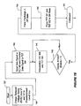
- a flow diagram illustrates a general method of operation of one embodiment of the present invention using as an example transmission of data packets from the source data port 1 to the destination data port 6 60.
- the each data packet is loaded 355 into its own data section 310a-f of the source data port 1 input buffer 110.
- Each data packet also includes a header that provides destination information indicating transmission to the destination data port 6 60 as well as priority information indicating the level of priority associated with each data packet.
- the system determines 360, through an arbitration process, whether the destination data port 6 is available to receive the data.
- the system transfers 365 the data packet in each data section 310a-f to the crossbar switch 105.
- Each data packet is transferred 365 from its respective data section 310a-f across its own dedicated data port 1 input path 115a-f that is coupled to the respective data section 310a-f.
- the data packet is then switched, or routed, 370 from the data port 1 input paths 115a-f to the data port 6 output path 168 and sent onto the destination data port 6 60. Because each data section has its own data path, the system does not require a separate arbitration process to transmit from the data input buffer 110 to the crossbar switch 105.
- the present invention demonstrates a benefit of each data packet and respective data section having its own dedicated input path directly coupled to the crossbar switch 105.
- One advantage of this implementation is having one arbitration process rather than two arbitration processes so that contention to gain access to the crossbar switch 105 is eliminated and the system now completes the arbitration process in one clock cycle. By eliminating the time and the system resources that were previously necessary for two arbitrations to transmit data packets across a single data port 1 input path to the crossbar switch 105, the speed of data signal transmission in the system is vastly improved.
- FIG. 5 a block diagram illustrates one embodiment of an internal portion of the present invention in which multiple source data ports attempt to transmit to at least one common destination data port.
- the system includes a crossbar switch 105, destination data ports 10, 20, 30, 40, 50, 60, source data port input buffers 110, 120, 130, 140, 150, 160, data input paths 115a-f, 125a-f, 135a-f, 145a-f, 155a-f, 165a-f, data output paths 118, 128, 138, 148, 158, 168, and crosspoint circuits 210.
- Each crosspoint circuit 210 is coupled to the data input paths 115a-f, 125a-f, 135a-f, 145a-f, 155a-f, 165a-f and the data output paths 118, 128, 138, 148, 158, 168 at an intersection of each of the two paths.
- a set of flow lines (dashed lines along the data paths) illustrate one example of the flow and potential flow of data packets from a source data port input buffer to a destination data port, as is further discussed below.
- a data packet from the source data port 1 being loaded and transmitted to the destination data port 6 60, similar to the process discussed above with respect to Figure 4.
- a data packet from the source data port 4 seeks to have data packets transmitted to the destination data port 2 20 through the data port 2 output path 128, to the destination data port 3 30 through the data port 3 output path 138, and to the destination data port 6 60 through the data port 6 output path 168.
- the data packets from the source data port 4 are loaded into the data sections of the source data port 4 input buffer 140 along with a header that provides destination information indicating whether that particular data packet is to be transmitted to the destination data port 2 20, the destination data port 3 30, or the destination data port 6 60.
- the header also includes priority information indicating the relative priority of that data packet compared to other data packets.
- the data packet in the first data section of the source data port 4 input buffer 140 is high priority and destined for the destination data port 6 60.
- the data packet in the second data section is medium priority and destined for the destination data port 3 30.
- the data packet in the fourth data section is low priority and destined for the destination data port 2 20.
- the arbitration unit 170 associated with the destination data port 6 60 does not grant access to the destination data port 6 60 because the source data port 1 is currently transmitting to the destination data port 6 60. However, the arbitration units 170 associated with the destination data port 2 20 and the destination data port 3 30 find that these data ports are available to receive the data packets.
- the present invention transmits the data packets destined for the destination data port 2 20 and the data packets destined for the destination data port 3 30 from the respective data sections, despite these data packets having lower priority than the data packet in the first data section.
- the present invention can transmit the lower priority data packets destined for the destination data port 2 20 and the destination data port 3 30 when the higher priority data packet destined for the destination data port 6 60 is unable to transmit due to the current transmission to the destination data port 6 60 from the data port 1.
- the dedicated data input path 140a-f for each data section of the source data port 4 input buffer eliminates the requirement that lower priority data packets wait for higher priority data packets to transmit to the crossbar switch 105.
- One embodiment of the present invention uses conventional arbitration, including conventional hardware, software, or a combination of hardware and software, to determine the availability of a particular data port or data ports.
- the present invention may use an arbitration device and method as is disclosed in the above-referenced U.S. Patent Application, Serial No. 081603880 , titled “METHOD AND APPARATUS FOR COORDINATING ACCESS TO AN OUTPUT OF A ROUTING DEVICE IN A PACKET SWITCHING NETWORK", filed on February 22. 1996, by Jeffrey D. Larson, Albert Mu, and Thomas M. Wicki.
- This embodiment of the present invention illustrates a benefit of a dedicated data input path 115a-f, 125a-f, 135a-f, 145a-f, 155a-f, 165a-f from each data section of a data input buffer 110, 120, 130, 140, 150, 160 to each data output path 110, 120, 130, 140, 150, 160 within the crossbar switch 105.
- the presence of each dedicated data input path 115a-f, 125a-f, 135a-f, 145a-f, 155a-f, 165a-f eliminates the initial arbitration previously required to first access a data input path leading to the crossbar switch 105.
- each dedicated data input path 115a-f, 125a-f, 135a-f, 145a-f, 155a-f, 165a-f also eliminates internal blocking problems because transmission of lower priority data packets to the crossbar switch 105 are permitted despite the presence of higher priority data packets that are waiting to be transmitted from other data sections of a source data port input buffer. Therefore, because there is no internal blocking occurring the present invention provides an advantage of faster data transmission through the crossbar switch 105.
- the crosspoint circuit 210 is a differential, reduced voltage swing circuit structure.
- the swing for switching states is typically 500 millivolts ("mV") due to the possibly large differential mode noise from the crossing and the adjacent conductors.
- the circuit includes a precharge circuit 401, a reduced voltage swing line V 1 402, and a reduced voltage swing line V2 403.
- the circuit For each data input path 115a-f, 125a-f, 135a-f, 145a-f, 155a-f 165a-f, the circuit includes a data line 410, an inverter 415, a set of field-effect transistors ("FETs"), such as FETs M 1 420, M2 430, M3 440, M4 450, and an enable line 405, so that in one embodiment of the present invention there are thirty-six (36) sets of such components along each data output path 118, 128, 138, 148, 158, 168.
- FETs field-effect transistors
- the crosspoint circuit includes a connection to a sense amplifier 480, sense amplifier lines A 460 and B 470, and a sense amplifier output line 490, so that in one embodiment of the present invention there are six (6) sets of such components, one along each data output path 118, 128, 138, 148, 158, 168.
- the precharge circuit 401 is coupled to the reduced voltage swing lines V1 402 and V2 403. Then, for each data input path 115a-f, 125a-f, 135a-f, 145a-f, 155a-f 165a-f, the enable line 405 is coupled to a gate of the FETs M1 420 and M2 430.
- the data line 410 is coupled to a gate of the FET M3 440, and to the inverter 415 that is coupled to a gate of the FET M4 450. For each data input path 115a-f, 125a-f, 135a-f, 145a-f, 155a-f 165a-f the data line 410 is coupled to the data input path.
- the data input path is the data line 410.
- the FET M 1 420 is coupled to the reduced voltage swing line V 1 402 and the FET M2 is coupled to the reduced voltage swing line V2 403.
- the FETs M1 420 and M3 440 form a transistor circuit as do the FETs M2 430 and M4 450.
- FETs M1 420 and M2 430 form a differential pair, as do FETs M3 440 and M4 450.
- the reduced voltage swing line V1 402 is coupled to the sense amplifier line A 460 while the reduced voltage swing line V2 403 is coupled to the sense amplifier line B 470.
- the sense amplifier lines A 460 and B 470 are coupled to the sense amplifier 480 which is coupled to the sense amplifier output line 490.
- the sense amplifier output line 490 is coupled to its respective data output path 118, 128, 138, 148, 158, 168.
- the data output path is the sense amplifier output line 490.
- Figure 7A is a flow diagram illustrating the general operation of one embodiment of the crosspoint circuit 210.
- a first reduced voltage swing line and a second reduced voltage swing line are charged 705 to a predetermined voltage level.
- the predetermined voltage level in the first reduced voltage swing line is discharged 710 while the predetermined voltage level in the second reduced voltage swing line is maintained 710.
- a clock signal is received 715 at the sense amplifier to turn it on, or place it in an on state.
- the sense amplifier Based upon a voltage differential between the first reduced voltage swing line V1 402 and the second reduced voltage swing line V2 403, the sense amplifier triggers 720 an output signal that produces 725 a full-swing output that is ultimately sent to the destination data port.
- FIG. 7B and 7C a flow diagram illustrates one embodiment of the operation of the crosspoint circuit 210 shown in Figure 6.
- the precharge circuit 401 turns on and an enable signal is inactive.
- the reduced voltage swing line V1 402 and the reduced voltage swing line V2 403 are charged 730 by the precharge circuit 401 so that both lines are charged to a predetermined voltage level such as Vcc volts of the power supply.
- a data signal is transmitted 735 along the data line 410 to the FET M3 440.
- the data signal is also inverted by inverter 415 and transmitted 735 to the FET M4 450.
- the data signal is loaded by preconditioning 740 the gates of both the FET M3 440 and the FET M4 450 so that the appropriate state of the data signal is reached.
- the system checks whether the enable signal has arrived 745. If there is no enable signal, the system continues to precondition the FET M3 440 and the FET M4 450.
- the precharge circuit 401 is placed 750 in an off state and the FET M1 420 and the FET M2 430 both are placed 755 in an on state.
- the enable signal is derived from the arbitration circuit 170 grant signal that is gated with a clock signal.
- the system determines 760 whether the data signal along data line 410 is a logic high, e.g., 1, at the time the enable signal arrives. If the data signal is high, the FET M1 420 and the FET M3 440 transistor circuit is placed 765 in an on state and the reduced voltage swing line V1 402 begins to discharge 770 to ground through this transistor circuit. Conversely, the FET M2 430 and the FET M4 450 transistor circuit is placed 770 in an off state because the inverted data line is a logic low. e.g., 0, thus turning off the FET M4 450.
- a logic high e.g., 1
- the voltage in the reduced voltage swing line V2 403 is maintained 770 at the Vcc level.
- the voltage level along the reduced voltage swing line V1 402 is transmitted 785 along sense amplifier line A 460 and the voltage level along the reduced voltage swing line V2 403 is transmitted 785 along sense amplifier line B 470, and the signals in both sense amplifier lines A 460 and B 470 are used to drive the sense amplifier 480.
- the sense amplifier 480 receives 790 a clock signal and turns on when the clock signal is high.
- the sense amplifier 480 When the sense amplifier 480 turns on, it generates 795 an output signal based on the voltage differential at that instant, that is at least 500 mV at an operating frequency of 200 megahertz ("Mhz"), between the reduced voltage swing line V1 402 and the reduced voltage swing line V2 403.
- the output signal that is produced 800 is a full-swing output of either 3.3 volts or ground (0 volts) depending upon the particular characteristics of the sense amplifier 480.
- the FET M3 is placed 775 in an off state and the FET M4 450 is placed 775 in an on state so that the FET M1 420, FET M3 440 circuit is in an off state and the FET M2 430, FET M4 450 circuit is in an on state.
- the voltage level in the reduced voltage swing line V1 402 is maintained 780 at Vcc volts.
- the voltage level in the reduced voltage swing line V2 is discharged 780 through the FET M2 430, FET M4 450 circuit that is in the on state.
- the voltage level in both the first reduced voltage swing line V1 402 and the second reduced voltage swing line V2 403 is transmitted 785 to the sense amplifier.
- the sense amplifier measures 790 the voltage differential between the voltage levels in the reduced voltage swing line V1 402 and the reduced voltage swing line V2 403.
- the sense amplifier 480 receives 790 a clock signal and turns on at the high clock signal.
- the sense amplifier 480 turns on and generates 795 an output signal based on the voltage differential at that instant between the voltage in the reduced voltage swing line V1 402 and the voltage in the reduced voltage swing line V2 403.
- the output signal that is produced 800 is a full-swing output of either 3.3 volts or ground (0 volts) depending upon the particular characteristics of the sense amplifier 480.
- the sense amplifier 480 is a conventional sense amplifier.
- the sense amplifier 480 may be a sense amplifier as described in the above-referenced U.S. Patent Application, Serial No.0 81603882 , titled "CLOCKED SENSE AMPLIFIER WITH POSITIVE SOURCE FEEDBACK", filed on February 22, 1996, by Albert Mu.
- the present invention permits the sense amplifier 480 to operate at a reduced voltage signal swing by generating a signal based upon the clock signal and the differential voltage rather than a full-swing voltage level.
- the system also produces a full-swing output signal by the sense amplifier 480 of either 3.3 volts or ground (0 volts) despite triggering or generating the output signal on a reduced swing differential.
- the full-swing signal is sent from the sense amplifier output line 490 to the data output path that is coupled to it.
- the reduced voltage swing crosspoint circuit allows multiple data input paths to connect to a bus of a crossbar switch without overburdening the bus.
- One advantage of this implementation is an increase in system speed because multiple data packets can transmit to and from the data port simultaneously over the bus of the crossbar switch, thereby providing an approach to eliminate internal blocking.
- the crosspoint circuit 210 may use a reduced differential swing operation to switch from one state to another state with a sufficient voltage differential rather than having to attain a particular voltage level. This increases system speed because the system does not need to wait for a particular voltage level in the reduced voltage swing lines before switching a state.
- Another advantage of this design is reduced power dissipation because of a reduced voltage swing on the data bus so that the overall power consumption of the chip is reduced. Moreover, generating or triggering an output signal based on the differential voltage reduces on-chip power drops that could adversely affect the system operation.
- FIG 8 is a graph of waveforms present during operation of one embodiment of the present invention.
- the waveforms include a clock signal, an enable signal, a data signal, a Vcc1 signal, and a Vcc2 signal.
- the enable signal is inactive and the precharge circuit 410 turns on so that the Vcc1 and the Vcc2 signal are at a voltage level of Vcc.
- the data signal into the system is at a high, or 1, state.
- the enable signal becomes active, the precharge circuit turns off or goes to an off state.
- the Vcc1 signal begins to discharge toward ground through FETs M1 and M3 because the data signal is at the high state.
- the Vcc2 signal remains at the Vcc voltage level.
- the sense amplifier turns on and generates or triggers an output signal based on the voltage differential between Vcc1 and Vcc2.
- the precharge circuit When another rising edge of the clock signal arrives, the precharge circuit turns on again or goes to an on state and the enable signal soon becomes inactive.
- the voltage signals Vcc1 and Vcc2 once again go to the voltage level of Vcc.
- the data signal may toggle to a low, or 0, state.
- the enable signal again becomes active, the precharge circuit turns off.
- the Vcc2 signal begins to discharge toward ground through FETs M2 and M4 because the data signal is at the low state.
- the Vcc1 signal remains at the Vcc voltage level.
- the sense amplifier On the rising edge of the clock signal the sense amplifier is again triggered in response to the differential between Vcc1 and Vcc2.
- the present invention has been described in a packet switching environment, the system and method of the present invention may apply to other switching environments, such as a circuit switching environment.
- a circuit switching environment In a circuit switching environment there is no buffering because there is no contention for the switch circuit.
Description
Claims (7)
- A switching system for selectively transferring data packets and including a switch, an input buffer (110) having a first data section (310a) and a second data section (310b), and a plurality of destination data ports, the system comprising:and the system further comprising:a first dedicated input path (115a) coupled to the first data section (310a) and a second dedicated input path (115b) coupled to the second data section (310b), for transferring data packets from the first data section and the second data section, respectively, to the switch;a plurality of output paths coupled to the destination data ports for transmitting the data packets to the destination data ports;wherein each reduced voltage swing crosspoint circuit generates a differential signal, and includes a precharge circuit (410) that is switchable to an off state prior to a discharging of the reduced voltage swing crosspoint circuit.a plurality of first reduced voltage swing crosspoint circuits (210) disposed in the switch each to couple the first dedicated input path and a respective one of the plurality of output paths, and a plurality of second reduced voltage swing crosspoint circuits (210) disposed in the switch each to couple the second input path and a respective one of the plurality of output paths, for switching the data packets from the first dedicated input path and the second dedicated input path, respectively, to the output paths,
- The switching system as to claim 1, wherein each reduced voltage swing circuit (210) further comprises a sense amplifier (480) for producing a full-swing output signal, the sense amplifier having a differential input for receiving the differential signal generated by the reduced voltage swing crosspoint circuit.
- The switching system as in claim 1, further comprising an arbitration unit for determining whether the destination data ports are available to receive the data packets, the arbitration unit coupled to the switch.
- The switching system as in claim 1, further comprising a circuit switching system.
- The switching system as in claim 1, the crosspoint circuit comprising:a first voltage line and a second voltage line, each voltage line coupled to the precharge unit (410) for carrying a predetermined voltage charge;a first transistor circuit coupled to the first voltage line for discharging the voltage charge in the first voltage line when a first transistor circuit is in an on state;a second transistor circuit coupled to the second voltage line for discharging the voltage charge in the second voltage line when a second transistor circuit is in an on state; ana sense amplifier, having an input for receiving a clock signal, a first input line, a second input line, and an output, the first input line coupled to the first voltage line and the second input line coupled to the second voltage line, for producing the full-swing output signal at the output when the clock signal is high and there is a differential voltage level between the voltage in an first voltage line and the voltage in the second voltage line.
- A method for transferring data in a switching system for selectively transferring data packets and including a switch, a plurality of output paths coupled to destination data ports, and an input buffer having a plurality of data sections, each data section coupled to a dedicated input path, the method comprising the steps of:wherein:loading a plurality of data packets into the plurality of data sections (310a, 310b, ... 310f);transferring each data packet to the switch over each dedicated input path coupled to each data section holding each data packet; andswitching each data packet from each dedicated input path to an output path (115a, 115b, ... 115f),the switching of each data packet from each dedicated input path to an output path is performed through reduced voltage swing crosspoint circuits (210), each such circuit arranged to couple a respective dedicated input path to a respective output path, andeach reduced voltage swing crosspoint circuit generates a differential signal, and includes a precharge circuit (480) that is switchable to an off state prior to a discharging of the reduced voltage swing crosspoint circuit.
- The method as in claim 6, further comprising the step of determining whether a destination data port is available to receive a data packet.
Applications Claiming Priority (3)
| Application Number | Priority Date | Filing Date | Title |
|---|---|---|---|
| US604920 | 1996-02-22 | ||
| US08/604,920 US5991296A (en) | 1996-02-22 | 1996-02-22 | Crossbar switch and method with reduced voltage swing and no internal blocking data path |
| PCT/US1997/002941 WO1997031463A2 (en) | 1996-02-22 | 1997-02-20 | Crossbar switch and method with reduced voltage swing and no internal blocking data path |
Publications (2)
| Publication Number | Publication Date |
|---|---|
| EP0840971A2 EP0840971A2 (en) | 1998-05-13 |
| EP0840971B1 true EP0840971B1 (en) | 2005-08-10 |
Family
ID=24421573
Family Applications (1)
| Application Number | Title | Priority Date | Filing Date |
|---|---|---|---|
| EP97908726A Expired - Lifetime EP0840971B1 (en) | 1996-02-22 | 1997-02-20 | Crossbar switch and method with reduced voltage swing and no internal blocking data path |
Country Status (5)
| Country | Link |
|---|---|
| US (2) | US5991296A (en) |
| EP (1) | EP0840971B1 (en) |
| JP (1) | JP3742112B2 (en) |
| DE (1) | DE69733931T2 (en) |
| WO (1) | WO1997031463A2 (en) |
Families Citing this family (71)
| Publication number | Priority date | Publication date | Assignee | Title |
|---|---|---|---|---|
| US5815681A (en) * | 1996-05-21 | 1998-09-29 | Elonex Plc Ltd. | Integrated network switching hub and bus structure |
| US6192048B1 (en) * | 1997-10-02 | 2001-02-20 | Mcdata Corporation | Method and apparatus for implementing hunt group support for a crosspoint controller |
| US6301637B1 (en) * | 1998-06-08 | 2001-10-09 | Storage Technology Corporation | High performance data paths |
| US7102999B1 (en) | 1999-11-24 | 2006-09-05 | Juniper Networks, Inc. | Switching device |
| GB0008195D0 (en) | 2000-04-05 | 2000-05-24 | Power X Limited | Data switching arbitration arrangements |
| US6965299B1 (en) * | 2000-04-19 | 2005-11-15 | Lsi Logic Corporation | High-speed, low-power crossbar switch |
| DE60129316D1 (en) | 2000-05-18 | 2007-08-23 | Xyratex Tech Ltd | DEVICE AND METHOD FOR FUNCTIONALIZATION OF THE AGENT |
| US6839795B1 (en) * | 2000-05-31 | 2005-01-04 | Silicon Labs Cp, Inc. | Priority cross-bar decoder |
| US7171542B1 (en) * | 2000-06-19 | 2007-01-30 | Silicon Labs Cp, Inc. | Reconfigurable interface for coupling functional input/output blocks to limited number of i/o pins |
| US8176296B2 (en) | 2000-10-26 | 2012-05-08 | Cypress Semiconductor Corporation | Programmable microcontroller architecture |
| US6724220B1 (en) | 2000-10-26 | 2004-04-20 | Cyress Semiconductor Corporation | Programmable microcontroller architecture (mixed analog/digital) |
| US8149048B1 (en) | 2000-10-26 | 2012-04-03 | Cypress Semiconductor Corporation | Apparatus and method for programmable power management in a programmable analog circuit block |
| US8103496B1 (en) | 2000-10-26 | 2012-01-24 | Cypress Semicondutor Corporation | Breakpoint control in an in-circuit emulation system |
| US7765095B1 (en) | 2000-10-26 | 2010-07-27 | Cypress Semiconductor Corporation | Conditional branching in an in-circuit emulation system |
| US8160864B1 (en) | 2000-10-26 | 2012-04-17 | Cypress Semiconductor Corporation | In-circuit emulator and pod synchronized boot |
| AU2002323268A1 (en) * | 2001-08-22 | 2003-03-10 | Avocent Corporation | Self-synchronizing half duplex matrix switch |
| US7237016B1 (en) | 2001-09-07 | 2007-06-26 | Palau Acquisition Corporation (Delaware) | Method and system to manage resource requests utilizing link-list queues within an arbiter associated with an interconnect device |
| US6950394B1 (en) | 2001-09-07 | 2005-09-27 | Agilent Technologies, Inc. | Methods and systems to transfer information using an alternative routing associated with a communication network |
| US7054330B1 (en) | 2001-09-07 | 2006-05-30 | Chou Norman C | Mask-based round robin arbitration |
| US6763418B1 (en) | 2001-09-07 | 2004-07-13 | Agilent Technologies, Inc. | Request bus arbitration |
| US6920106B1 (en) | 2001-09-07 | 2005-07-19 | Agilent Technologies, Inc. | Speculative loading of buffers within a port of a network device |
| US7136379B2 (en) * | 2001-10-10 | 2006-11-14 | Qualcomm Incorporated | Multiple-interface port multiplexer |
| US7209476B1 (en) | 2001-10-12 | 2007-04-24 | Avago Technologies General Ip (Singapore) Pte. Ltd. | Method and apparatus for input/output port mirroring for networking system bring-up and debug |
| US6839794B1 (en) | 2001-10-12 | 2005-01-04 | Agilent Technologies, Inc. | Method and system to map a service level associated with a packet to one of a number of data streams at an interconnect device |
| US6922749B1 (en) | 2001-10-12 | 2005-07-26 | Agilent Technologies, Inc. | Apparatus and methodology for an input port of a switch that supports cut-through operation within the switch |
| US7406674B1 (en) | 2001-10-24 | 2008-07-29 | Cypress Semiconductor Corporation | Method and apparatus for generating microcontroller configuration information |
| US8078970B1 (en) | 2001-11-09 | 2011-12-13 | Cypress Semiconductor Corporation | Graphical user interface with user-selectable list-box |
| US8042093B1 (en) | 2001-11-15 | 2011-10-18 | Cypress Semiconductor Corporation | System providing automatic source code generation for personalization and parameterization of user modules |
| US7774190B1 (en) | 2001-11-19 | 2010-08-10 | Cypress Semiconductor Corporation | Sleep and stall in an in-circuit emulation system |
| US7770113B1 (en) | 2001-11-19 | 2010-08-03 | Cypress Semiconductor Corporation | System and method for dynamically generating a configuration datasheet |
| US8069405B1 (en) | 2001-11-19 | 2011-11-29 | Cypress Semiconductor Corporation | User interface for efficiently browsing an electronic document using data-driven tabs |
| US6971004B1 (en) | 2001-11-19 | 2005-11-29 | Cypress Semiconductor Corp. | System and method of dynamically reconfiguring a programmable integrated circuit |
| US7844437B1 (en) | 2001-11-19 | 2010-11-30 | Cypress Semiconductor Corporation | System and method for performing next placements and pruning of disallowed placements for programming an integrated circuit |
| FR2833441A1 (en) * | 2001-12-11 | 2003-06-13 | Koninkl Philips Electronics Nv | Optical transmission rate packet switching mechanism having matrix function control system and decoder finding switching states with local decoder interconnection point level signal control providing. |
| FR2833449A1 (en) * | 2001-12-11 | 2003-06-13 | Koninkl Philips Electronics Nv | High digital transmission rate switching circuit, for optical communication, having interconnection matrix controlled signal and reference transmissions and two distinct lines having common voltage reference channel |
| US8103497B1 (en) | 2002-03-28 | 2012-01-24 | Cypress Semiconductor Corporation | External interface for event architecture |
| US7016996B1 (en) | 2002-04-15 | 2006-03-21 | Schober Richard L | Method and apparatus to detect a timeout condition for a data item within a process |
| US7308608B1 (en) | 2002-05-01 | 2007-12-11 | Cypress Semiconductor Corporation | Reconfigurable testing system and method |
| US7761845B1 (en) | 2002-09-09 | 2010-07-20 | Cypress Semiconductor Corporation | Method for parameterizing a user module |
| JP2005267502A (en) * | 2004-03-22 | 2005-09-29 | Hitachi Ltd | Switch for data transfer |
| US7295049B1 (en) | 2004-03-25 | 2007-11-13 | Cypress Semiconductor Corporation | Method and circuit for rapid alignment of signals |
| US8069436B2 (en) | 2004-08-13 | 2011-11-29 | Cypress Semiconductor Corporation | Providing hardware independence to automate code generation of processing device firmware |
| US8286125B2 (en) | 2004-08-13 | 2012-10-09 | Cypress Semiconductor Corporation | Model for a hardware device-independent method of defining embedded firmware for programmable systems |
| US7332976B1 (en) | 2005-02-04 | 2008-02-19 | Cypress Semiconductor Corporation | Poly-phase frequency synthesis oscillator |
| US7400183B1 (en) | 2005-05-05 | 2008-07-15 | Cypress Semiconductor Corporation | Voltage controlled oscillator delay cell and method |
| US8089461B2 (en) | 2005-06-23 | 2012-01-03 | Cypress Semiconductor Corporation | Touch wake for electronic devices |
| US20070097858A1 (en) * | 2005-11-01 | 2007-05-03 | Lesartre Gregg B | Method and computer system for employing an interconnection fabric providing multiple communication paths |
| US8085067B1 (en) | 2005-12-21 | 2011-12-27 | Cypress Semiconductor Corporation | Differential-to-single ended signal converter circuit and method |
| US9098641B1 (en) * | 2006-01-30 | 2015-08-04 | Cypress Semiconductor Corporation | Configurable bus |
| US8067948B2 (en) | 2006-03-27 | 2011-11-29 | Cypress Semiconductor Corporation | Input/output multiplexer bus |
| US20070268895A1 (en) * | 2006-05-19 | 2007-11-22 | Motorola, Inc. | Method and apparatus for switching data |
| US9564902B2 (en) | 2007-04-17 | 2017-02-07 | Cypress Semiconductor Corporation | Dynamically configurable and re-configurable data path |
| US8130025B2 (en) | 2007-04-17 | 2012-03-06 | Cypress Semiconductor Corporation | Numerical band gap |
| US8026739B2 (en) | 2007-04-17 | 2011-09-27 | Cypress Semiconductor Corporation | System level interconnect with programmable switching |
| US7737724B2 (en) | 2007-04-17 | 2010-06-15 | Cypress Semiconductor Corporation | Universal digital block interconnection and channel routing |
| US8040266B2 (en) | 2007-04-17 | 2011-10-18 | Cypress Semiconductor Corporation | Programmable sigma-delta analog-to-digital converter |
| US8516025B2 (en) | 2007-04-17 | 2013-08-20 | Cypress Semiconductor Corporation | Clock driven dynamic datapath chaining |
| US8092083B2 (en) | 2007-04-17 | 2012-01-10 | Cypress Semiconductor Corporation | Temperature sensor with digital bandgap |
| US8065653B1 (en) | 2007-04-25 | 2011-11-22 | Cypress Semiconductor Corporation | Configuration of programmable IC design elements |
| US9720805B1 (en) | 2007-04-25 | 2017-08-01 | Cypress Semiconductor Corporation | System and method for controlling a target device |
| US8266575B1 (en) | 2007-04-25 | 2012-09-11 | Cypress Semiconductor Corporation | Systems and methods for dynamically reconfiguring a programmable system on a chip |
| US8049569B1 (en) | 2007-09-05 | 2011-11-01 | Cypress Semiconductor Corporation | Circuit and method for improving the accuracy of a crystal-less oscillator having dual-frequency modes |
| US8230152B2 (en) * | 2009-02-13 | 2012-07-24 | The Regents Of The University Of Michigan | Crossbar circuitry and method of operation of such crossbar circuitry |
| US8255610B2 (en) | 2009-02-13 | 2012-08-28 | The Regents Of The University Of Michigan | Crossbar circuitry for applying a pre-selection prior to arbitration between transmission requests and method of operation of such crossbar circuitry |
| US8108585B2 (en) | 2009-02-13 | 2012-01-31 | The Regents Of The Universtiy Of Michigan | Crossbar circuitry and method of operation of such crossbar circuitry |
| US8549207B2 (en) * | 2009-02-13 | 2013-10-01 | The Regents Of The University Of Michigan | Crossbar circuitry for applying an adaptive priority scheme and method of operation of such crossbar circuitry |
| US8868817B2 (en) | 2009-02-13 | 2014-10-21 | The Regents Of The University Of Michigan | Crossbar circuitry for applying an adaptive priority scheme and method of operation of such crossbar circuitry |
| US9514074B2 (en) | 2009-02-13 | 2016-12-06 | The Regents Of The University Of Michigan | Single cycle arbitration within an interconnect |
| US9448964B2 (en) | 2009-05-04 | 2016-09-20 | Cypress Semiconductor Corporation | Autonomous control in a programmable system |
| US8583850B2 (en) * | 2011-02-14 | 2013-11-12 | Oracle America, Inc. | Micro crossbar switch and on-die data network using the same |
| CN104123261B (en) * | 2014-07-01 | 2017-06-27 | 联想(北京)有限公司 | A kind of electronic equipment and information transferring method |
Family Cites Families (45)
| Publication number | Priority date | Publication date | Assignee | Title |
|---|---|---|---|---|
| US35483A (en) * | 1862-06-03 | Improvement in cooking-stoves | ||
| US4058838A (en) * | 1976-11-10 | 1977-11-15 | International Telephone And Telegraph Corporation | Packet-switched facsimile communications system |
| GB2032736B (en) * | 1978-10-24 | 1982-09-08 | Standard Telephones Cables Ltd | Data transfer system |
| US4412380A (en) * | 1981-09-02 | 1983-11-01 | Murray Corporation | Hose cutoff device or tool |
| US4434381A (en) * | 1981-12-07 | 1984-02-28 | Rca Corporation | Sense amplifiers |
| LU86787A1 (en) * | 1986-06-19 | 1987-07-24 | Siemens Ag | BROADBAND SIGNAL DEVICE |
| LU87147A1 (en) * | 1987-10-14 | 1988-07-14 | Siemens Ag | BROADBAND SIGNAL DEVICE |
| US5285445A (en) * | 1987-12-17 | 1994-02-08 | U.S. Philips Corporation | Switching network and switching network control for a switching node in a wideband transmission system |
| JPH01177239A (en) * | 1988-01-06 | 1989-07-13 | Nec Corp | Packet concentrator and packet switching device |
| US4995056A (en) * | 1989-01-13 | 1991-02-19 | International Business Machines Corporation | System and method for data communications |
| US4965793A (en) * | 1989-02-03 | 1990-10-23 | Digital Equipment Corporation | Method and apparatus for interfacing a system control unit for a multi-processor |
| US5091879A (en) * | 1989-02-14 | 1992-02-25 | Texas Instruments Incorporated | BiCMOS static memory with improved performance stability |
| US5138615A (en) * | 1989-06-22 | 1992-08-11 | Digital Equipment Corporation | Reconfiguration system and method for high-speed mesh connected local area network |
| GB8915137D0 (en) * | 1989-06-30 | 1989-08-23 | Inmos Ltd | Message routing |
| GB8915135D0 (en) * | 1989-06-30 | 1989-08-23 | Inmos Ltd | Message routing |
| CA2015514C (en) * | 1989-08-22 | 1996-08-06 | Mitsuru Tsuboi | Packet switching system having bus matrix switch |
| JP2531275B2 (en) * | 1989-09-29 | 1996-09-04 | 日本電気株式会社 | ATM cell transfer method |
| US4999829A (en) * | 1989-11-06 | 1991-03-12 | At&T Bell Laboratories | Automatic fault recovery in a packet network |
| US5166926A (en) * | 1990-12-18 | 1992-11-24 | Bell Communications Research, Inc. | Packet address look-ahead technique for use in implementing a high speed packet switch |
| US5226014A (en) * | 1990-12-24 | 1993-07-06 | Ncr Corporation | Low power pseudo-static ROM |
| US5384773A (en) * | 1991-03-29 | 1995-01-24 | International Business Machines Corp. | Multi-media analog/digital/optical switching apparatus |
| US5257236A (en) * | 1991-08-01 | 1993-10-26 | Silicon Engineering, Inc. | Static RAM |
| US5241536A (en) * | 1991-10-03 | 1993-08-31 | Northern Telecom Limited | Broadband input buffered atm switch |
| US5345228A (en) * | 1991-10-31 | 1994-09-06 | International Business Machines Corporation | Very large scale modular switch |
| JPH05199255A (en) * | 1992-01-18 | 1993-08-06 | Mitsubishi Electric Corp | Electronic cross point switch device |
| SE515178C2 (en) * | 1992-03-20 | 2001-06-25 | Ericsson Telefon Ab L M | Procedures and devices for prioritizing buffer management in packet networks |
| US5255265A (en) * | 1992-05-05 | 1993-10-19 | At&T Bell Laboratories | Controller for input-queued packet switch |
| US5267235A (en) * | 1992-05-21 | 1993-11-30 | Digital Equipment Corporation | Method and apparatus for resource arbitration |
| US5473755A (en) * | 1992-06-01 | 1995-12-05 | Intel Corporation | System for controlling data stream by changing fall through FIFO last cell state of first component whenever data read out of second component last latch |
| JP3384838B2 (en) * | 1992-06-29 | 2003-03-10 | シャープ株式会社 | Interface device |
| DE4226599C2 (en) * | 1992-08-11 | 1994-08-04 | Siemens Ag | Error detection method in digital communication systems |
| MX9306994A (en) * | 1992-12-15 | 1994-06-30 | Ericsson Telefon Ab L M | FLOW CONTROL SYSTEM FOR PACKAGE SWITCHES. |
| EP0602693B1 (en) * | 1992-12-18 | 2001-11-21 | Alcatel | ATM switching node and ATM switching element having routing logic means |
| US5406554A (en) * | 1993-10-05 | 1995-04-11 | Music Semiconductors, Corp. | Synchronous FIFO having an alterable buffer store |
| US5613067A (en) * | 1993-12-30 | 1997-03-18 | International Business Machines Corporation | Method and apparatus for assuring that multiple messages in a multi-node network are assured fair access to an outgoing data stream |
| JPH07235939A (en) * | 1994-02-22 | 1995-09-05 | Fujitsu Ltd | Traffic scattering device/method, and repeating installation and terminal equipment |
| US5508644A (en) * | 1994-09-28 | 1996-04-16 | Motorola, Inc. | Sense amplifier for differential voltage detection with low input capacitance |
| US5517495A (en) * | 1994-12-06 | 1996-05-14 | At&T Corp. | Fair prioritized scheduling in an input-buffered switch |
| US5541919A (en) * | 1994-12-19 | 1996-07-30 | Motorola, Inc. | Multimedia multiplexing device and method using dynamic packet segmentation |
| US5619497A (en) * | 1994-12-22 | 1997-04-08 | Emc Corporation | Method and apparatus for reordering frames |
| US5502680A (en) * | 1995-02-16 | 1996-03-26 | Cirrus Logic Inc | Sense amplifier with pull-up circuit for accelerated latching of logic level output data |
| US5544161A (en) * | 1995-03-28 | 1996-08-06 | Bell Atlantic Network Services, Inc. | ATM packet demultiplexer for use in full service network having distributed architecture |
| US5689500A (en) * | 1996-01-16 | 1997-11-18 | Lucent Technologies, Inc. | Multistage network having multicast routing congestion feedback |
| US6028801A (en) * | 1998-06-29 | 2000-02-22 | Conexant Systems, Inc. | High speed sensing of dual port static RAM cell |
| US6240026B1 (en) * | 2000-03-07 | 2001-05-29 | Stmicroelectronics, Inc. | Bit line sense circuit and method for dynamic random access memories |
-
1996
- 1996-02-22 US US08/604,920 patent/US5991296A/en not_active Expired - Lifetime
-
1997
- 1997-02-20 EP EP97908726A patent/EP0840971B1/en not_active Expired - Lifetime
- 1997-02-20 JP JP53040597A patent/JP3742112B2/en not_active Expired - Fee Related
- 1997-02-20 WO PCT/US1997/002941 patent/WO1997031463A2/en active IP Right Grant
- 1997-02-20 DE DE69733931T patent/DE69733931T2/en not_active Expired - Lifetime
-
1999
- 1999-10-14 US US09/419,702 patent/US6490213B1/en not_active Expired - Fee Related
Also Published As
| Publication number | Publication date |
|---|---|
| WO1997031463A2 (en) | 1997-08-28 |
| US6490213B1 (en) | 2002-12-03 |
| JPH11511633A (en) | 1999-10-05 |
| DE69733931D1 (en) | 2005-09-15 |
| US5991296A (en) | 1999-11-23 |
| EP0840971A2 (en) | 1998-05-13 |
| JP3742112B2 (en) | 2006-02-01 |
| DE69733931T2 (en) | 2006-05-11 |
| WO1997031463A3 (en) | 1997-12-04 |
Similar Documents
| Publication | Publication Date | Title |
|---|---|---|
| EP0840971B1 (en) | Crossbar switch and method with reduced voltage swing and no internal blocking data path | |
| Wielage et al. | Networks on silicon: blessing or nightmare? | |
| EP1744497B1 (en) | Method for managing a plurality of virtual links shared on a communication line and network implementing said method | |
| EP0405208B1 (en) | Multistage network with distributed pipelined control | |
| JP3383846B2 (en) | SAM with expandable data width for multiport RAM | |
| US4929940A (en) | Collision crossbar switch | |
| WO1997012494A1 (en) | An asymmetric switch architecture for use in a network switch node | |
| US6697362B1 (en) | Distributed switch memory architecture | |
| JP2644134B2 (en) | Parallel processor system and switch queuing structure used in the system | |
| US7535898B2 (en) | Distributed switch memory architecture | |
| JPH09247204A (en) | Lan switch | |
| US6005863A (en) | Frame switch with serial data processing | |
| US5130976A (en) | Batcher and banyan switching elements | |
| Akata et al. | A 250-Mb/s 32* 32 CMOS crosspoint LSI for ATM switching systems | |
| US6993018B1 (en) | Priority signaling for cell switching | |
| US20100002581A1 (en) | Method for Inter-Router Dual-Function Energy- and Area-Efficient Links for Network-on-Chips | |
| WO2006089559A1 (en) | A network, a system and a node for use in the network or system | |
| US5774653A (en) | High-throughput data buffer | |
| US5039986A (en) | High speed dynamic allocator for various length time slots | |
| EP0369116B1 (en) | TDM switching matrix controller | |
| Yorozu et al. | Single flux quantum packet switch circuits for large-scale communication systems | |
| Luo et al. | A low power and delay multi-protocol switch with IO and network virtualization | |
| KR100371139B1 (en) | Crosspoint Element for ATM Switching Apparatus | |
| JP2024514888A (en) | Localized NOC switching interconnect for high bandwidth interfaces | |
| Weeks et al. | A prototype chipset for a large scaleable ATM switching node |
Legal Events
| Date | Code | Title | Description |
|---|---|---|---|
| PUAI | Public reference made under article 153(3) epc to a published international application that has entered the european phase |
Free format text: ORIGINAL CODE: 0009012 |
|
| 17P | Request for examination filed |
Effective date: 19971114 |
|
| AK | Designated contracting states |
Kind code of ref document: A2 Designated state(s): DE FR GB |
|
| 17Q | First examination report despatched |
Effective date: 20030620 |
|
| GRAP | Despatch of communication of intention to grant a patent |
Free format text: ORIGINAL CODE: EPIDOSNIGR1 |
|
| GRAS | Grant fee paid |
Free format text: ORIGINAL CODE: EPIDOSNIGR3 |
|
| GRAA | (expected) grant |
Free format text: ORIGINAL CODE: 0009210 |
|
| AK | Designated contracting states |
Kind code of ref document: B1 Designated state(s): DE FR GB |
|
| RAP1 | Party data changed (applicant data changed or rights of an application transferred) |
Owner name: FUJITSU LIMITED |
|
| REG | Reference to a national code |
Ref country code: GB Ref legal event code: FG4D |
|
| REF | Corresponds to: |
Ref document number: 69733931 Country of ref document: DE Date of ref document: 20050915 Kind code of ref document: P |
|
| ET | Fr: translation filed | ||
| PLBE | No opposition filed within time limit |
Free format text: ORIGINAL CODE: 0009261 |
|
| STAA | Information on the status of an ep patent application or granted ep patent |
Free format text: STATUS: NO OPPOSITION FILED WITHIN TIME LIMIT |
|
| 26N | No opposition filed |
Effective date: 20060511 |
|
| PGFP | Annual fee paid to national office [announced via postgrant information from national office to epo] |
Ref country code: DE Payment date: 20130213 Year of fee payment: 17 Ref country code: GB Payment date: 20130220 Year of fee payment: 17 Ref country code: FR Payment date: 20130301 Year of fee payment: 17 |
|
| REG | Reference to a national code |
Ref country code: DE Ref legal event code: R119 Ref document number: 69733931 Country of ref document: DE |
|
| REG | Reference to a national code |
Ref country code: DE Ref legal event code: R079 Ref document number: 69733931 Country of ref document: DE Free format text: PREVIOUS MAIN CLASS: H04L0012560000 Ipc: H04L0012933000 |
|
| GBPC | Gb: european patent ceased through non-payment of renewal fee |
Effective date: 20140220 |
|
| REG | Reference to a national code |
Ref country code: FR Ref legal event code: ST Effective date: 20141031 |
|
| REG | Reference to a national code |
Ref country code: DE Ref legal event code: R119 Ref document number: 69733931 Country of ref document: DE Effective date: 20140902 Ref country code: DE Ref legal event code: R079 Ref document number: 69733931 Country of ref document: DE Free format text: PREVIOUS MAIN CLASS: H04L0012560000 Ipc: H04L0012933000 Effective date: 20141020 |
|
| PG25 | Lapsed in a contracting state [announced via postgrant information from national office to epo] |
Ref country code: GB Free format text: LAPSE BECAUSE OF NON-PAYMENT OF DUE FEES Effective date: 20140220 Ref country code: DE Free format text: LAPSE BECAUSE OF NON-PAYMENT OF DUE FEES Effective date: 20140902 Ref country code: FR Free format text: LAPSE BECAUSE OF NON-PAYMENT OF DUE FEES Effective date: 20140228 |