EP0834773A2 - Focusing and tilting adjustment system for lithography aligner, manufacturing apparatus or inspection apparatus - Google Patents
Focusing and tilting adjustment system for lithography aligner, manufacturing apparatus or inspection apparatus Download PDFInfo
- Publication number
- EP0834773A2 EP0834773A2 EP97307868A EP97307868A EP0834773A2 EP 0834773 A2 EP0834773 A2 EP 0834773A2 EP 97307868 A EP97307868 A EP 97307868A EP 97307868 A EP97307868 A EP 97307868A EP 0834773 A2 EP0834773 A2 EP 0834773A2
- Authority
- EP
- European Patent Office
- Prior art keywords
- detection
- substrate
- focus
- projection
- detection system
- Prior art date
- Legal status (The legal status is an assumption and is not a legal conclusion. Google has not performed a legal analysis and makes no representation as to the accuracy of the status listed.)
- Withdrawn
Links
Images


Classifications
-
- H—ELECTRICITY
- H01—ELECTRIC ELEMENTS
- H01L—SEMICONDUCTOR DEVICES NOT COVERED BY CLASS H10
- H01L21/00—Processes or apparatus adapted for the manufacture or treatment of semiconductor or solid state devices or of parts thereof
- H01L21/02—Manufacture or treatment of semiconductor devices or of parts thereof
- H01L21/027—Making masks on semiconductor bodies for further photolithographic processing not provided for in group H01L21/18 or H01L21/34
-
- G—PHYSICS
- G03—PHOTOGRAPHY; CINEMATOGRAPHY; ANALOGOUS TECHNIQUES USING WAVES OTHER THAN OPTICAL WAVES; ELECTROGRAPHY; HOLOGRAPHY
- G03F—PHOTOMECHANICAL PRODUCTION OF TEXTURED OR PATTERNED SURFACES, e.g. FOR PRINTING, FOR PROCESSING OF SEMICONDUCTOR DEVICES; MATERIALS THEREFOR; ORIGINALS THEREFOR; APPARATUS SPECIALLY ADAPTED THEREFOR
- G03F7/00—Photomechanical, e.g. photolithographic, production of textured or patterned surfaces, e.g. printing surfaces; Materials therefor, e.g. comprising photoresists; Apparatus specially adapted therefor
- G03F7/70—Microphotolithographic exposure; Apparatus therefor
- G03F7/70483—Information management; Active and passive control; Testing; Wafer monitoring, e.g. pattern monitoring
- G03F7/70605—Workpiece metrology
- G03F7/70616—Monitoring the printed patterns
- G03F7/70641—Focus
-
- G—PHYSICS
- G03—PHOTOGRAPHY; CINEMATOGRAPHY; ANALOGOUS TECHNIQUES USING WAVES OTHER THAN OPTICAL WAVES; ELECTROGRAPHY; HOLOGRAPHY
- G03F—PHOTOMECHANICAL PRODUCTION OF TEXTURED OR PATTERNED SURFACES, e.g. FOR PRINTING, FOR PROCESSING OF SEMICONDUCTOR DEVICES; MATERIALS THEREFOR; ORIGINALS THEREFOR; APPARATUS SPECIALLY ADAPTED THEREFOR
- G03F7/00—Photomechanical, e.g. photolithographic, production of textured or patterned surfaces, e.g. printing surfaces; Materials therefor, e.g. comprising photoresists; Apparatus specially adapted therefor
- G03F7/70—Microphotolithographic exposure; Apparatus therefor
- G03F7/70216—Mask projection systems
- G03F7/70275—Multiple projection paths, e.g. array of projection systems, microlens projection systems or tandem projection systems
-
- G—PHYSICS
- G03—PHOTOGRAPHY; CINEMATOGRAPHY; ANALOGOUS TECHNIQUES USING WAVES OTHER THAN OPTICAL WAVES; ELECTROGRAPHY; HOLOGRAPHY
- G03F—PHOTOMECHANICAL PRODUCTION OF TEXTURED OR PATTERNED SURFACES, e.g. FOR PRINTING, FOR PROCESSING OF SEMICONDUCTOR DEVICES; MATERIALS THEREFOR; ORIGINALS THEREFOR; APPARATUS SPECIALLY ADAPTED THEREFOR
- G03F7/00—Photomechanical, e.g. photolithographic, production of textured or patterned surfaces, e.g. printing surfaces; Materials therefor, e.g. comprising photoresists; Apparatus specially adapted therefor
- G03F7/70—Microphotolithographic exposure; Apparatus therefor
- G03F7/70216—Mask projection systems
- G03F7/70341—Details of immersion lithography aspects, e.g. exposure media or control of immersion liquid supply
-
- G—PHYSICS
- G03—PHOTOGRAPHY; CINEMATOGRAPHY; ANALOGOUS TECHNIQUES USING WAVES OTHER THAN OPTICAL WAVES; ELECTROGRAPHY; HOLOGRAPHY
- G03F—PHOTOMECHANICAL PRODUCTION OF TEXTURED OR PATTERNED SURFACES, e.g. FOR PRINTING, FOR PROCESSING OF SEMICONDUCTOR DEVICES; MATERIALS THEREFOR; ORIGINALS THEREFOR; APPARATUS SPECIALLY ADAPTED THEREFOR
- G03F7/00—Photomechanical, e.g. photolithographic, production of textured or patterned surfaces, e.g. printing surfaces; Materials therefor, e.g. comprising photoresists; Apparatus specially adapted therefor
- G03F7/70—Microphotolithographic exposure; Apparatus therefor
- G03F7/70216—Mask projection systems
- G03F7/70358—Scanning exposure, i.e. relative movement of patterned beam and workpiece during imaging
-
- G—PHYSICS
- G03—PHOTOGRAPHY; CINEMATOGRAPHY; ANALOGOUS TECHNIQUES USING WAVES OTHER THAN OPTICAL WAVES; ELECTROGRAPHY; HOLOGRAPHY
- G03F—PHOTOMECHANICAL PRODUCTION OF TEXTURED OR PATTERNED SURFACES, e.g. FOR PRINTING, FOR PROCESSING OF SEMICONDUCTOR DEVICES; MATERIALS THEREFOR; ORIGINALS THEREFOR; APPARATUS SPECIALLY ADAPTED THEREFOR
- G03F7/00—Photomechanical, e.g. photolithographic, production of textured or patterned surfaces, e.g. printing surfaces; Materials therefor, e.g. comprising photoresists; Apparatus specially adapted therefor
- G03F7/70—Microphotolithographic exposure; Apparatus therefor
- G03F7/70691—Handling of masks or workpieces
- G03F7/70716—Stages
-
- G—PHYSICS
- G03—PHOTOGRAPHY; CINEMATOGRAPHY; ANALOGOUS TECHNIQUES USING WAVES OTHER THAN OPTICAL WAVES; ELECTROGRAPHY; HOLOGRAPHY
- G03F—PHOTOMECHANICAL PRODUCTION OF TEXTURED OR PATTERNED SURFACES, e.g. FOR PRINTING, FOR PROCESSING OF SEMICONDUCTOR DEVICES; MATERIALS THEREFOR; ORIGINALS THEREFOR; APPARATUS SPECIALLY ADAPTED THEREFOR
- G03F7/00—Photomechanical, e.g. photolithographic, production of textured or patterned surfaces, e.g. printing surfaces; Materials therefor, e.g. comprising photoresists; Apparatus specially adapted therefor
- G03F7/70—Microphotolithographic exposure; Apparatus therefor
- G03F7/708—Construction of apparatus, e.g. environment aspects, hygiene aspects or materials
- G03F7/70808—Construction details, e.g. housing, load-lock, seals or windows for passing light in or out of apparatus
-
- G—PHYSICS
- G03—PHOTOGRAPHY; CINEMATOGRAPHY; ANALOGOUS TECHNIQUES USING WAVES OTHER THAN OPTICAL WAVES; ELECTROGRAPHY; HOLOGRAPHY
- G03F—PHOTOMECHANICAL PRODUCTION OF TEXTURED OR PATTERNED SURFACES, e.g. FOR PRINTING, FOR PROCESSING OF SEMICONDUCTOR DEVICES; MATERIALS THEREFOR; ORIGINALS THEREFOR; APPARATUS SPECIALLY ADAPTED THEREFOR
- G03F7/00—Photomechanical, e.g. photolithographic, production of textured or patterned surfaces, e.g. printing surfaces; Materials therefor, e.g. comprising photoresists; Apparatus specially adapted therefor
- G03F7/70—Microphotolithographic exposure; Apparatus therefor
- G03F7/708—Construction of apparatus, e.g. environment aspects, hygiene aspects or materials
- G03F7/70858—Environment aspects, e.g. pressure of beam-path gas, temperature
- G03F7/70866—Environment aspects, e.g. pressure of beam-path gas, temperature of mask or workpiece
- G03F7/70875—Temperature, e.g. temperature control of masks or workpieces via control of stage temperature
-
- G—PHYSICS
- G03—PHOTOGRAPHY; CINEMATOGRAPHY; ANALOGOUS TECHNIQUES USING WAVES OTHER THAN OPTICAL WAVES; ELECTROGRAPHY; HOLOGRAPHY
- G03F—PHOTOMECHANICAL PRODUCTION OF TEXTURED OR PATTERNED SURFACES, e.g. FOR PRINTING, FOR PROCESSING OF SEMICONDUCTOR DEVICES; MATERIALS THEREFOR; ORIGINALS THEREFOR; APPARATUS SPECIALLY ADAPTED THEREFOR
- G03F7/00—Photomechanical, e.g. photolithographic, production of textured or patterned surfaces, e.g. printing surfaces; Materials therefor, e.g. comprising photoresists; Apparatus specially adapted therefor
- G03F7/70—Microphotolithographic exposure; Apparatus therefor
- G03F7/708—Construction of apparatus, e.g. environment aspects, hygiene aspects or materials
- G03F7/70858—Environment aspects, e.g. pressure of beam-path gas, temperature
- G03F7/70883—Environment aspects, e.g. pressure of beam-path gas, temperature of optical system
- G03F7/70891—Temperature
-
- G—PHYSICS
- G03—PHOTOGRAPHY; CINEMATOGRAPHY; ANALOGOUS TECHNIQUES USING WAVES OTHER THAN OPTICAL WAVES; ELECTROGRAPHY; HOLOGRAPHY
- G03F—PHOTOMECHANICAL PRODUCTION OF TEXTURED OR PATTERNED SURFACES, e.g. FOR PRINTING, FOR PROCESSING OF SEMICONDUCTOR DEVICES; MATERIALS THEREFOR; ORIGINALS THEREFOR; APPARATUS SPECIALLY ADAPTED THEREFOR
- G03F9/00—Registration or positioning of originals, masks, frames, photographic sheets or textured or patterned surfaces, e.g. automatically
- G03F9/70—Registration or positioning of originals, masks, frames, photographic sheets or textured or patterned surfaces, e.g. automatically for microlithography
- G03F9/7003—Alignment type or strategy, e.g. leveling, global alignment
- G03F9/7023—Aligning or positioning in direction perpendicular to substrate surface
- G03F9/7026—Focusing
Definitions
- the present invention relates to semiconductor fabrication and more particularly to a lithography exposure apparatus (aligner) for transferring a circuit pattern from a mask or a reticle onto a sensitive substrate.
- a lithography exposure apparatus for transferring a circuit pattern from a mask or a reticle onto a sensitive substrate.
- the present invention also relates to a system for detecting a focal point on a workpiece (wafer,substrate or plate etc.) and for detecting a tilt of the workpiece, which is applicable to certain kinds of apparatus such as an apparatus for manufacturing a workpiece or imaging a desired pattern in a surface of a workpiece using a laser or electron beam and an apparatus for optically inspecting the state of a surface of a workpiece.
- DRAMs dynamic random access memory semiconductor chips having an integration density of 64 Mbits
- Such chips are manufactured by exposing a semiconductor wafer to images of circuit patterns to form e.g. ten or more layers of circuit patterns in a superposition manner.
- lithography apparatuses used for such chip fabrication are projection aligners in which a circuit pattern drawn in a chromium layer on a reticle (mask plate) is transferred onto a resist layer on a wafer surface through a 1/4 or 1/5 reduction optical imaging system by irradiating the reticle with i-line radiation (wavelength: 365 nm) of a mercury discharge lamp or pulse light having a wavelength of 248 nm from a KrF excimer laser.
- i-line radiation wavelength: 365 nm
- Projection exposure apparatuses used for this purpose are generally grouped, according to the types of imaging optical system, into those using a step-and-repeat system, i.e., so-called steppers, and those using a step-and-scan system which has attracted attention in recent years.
- a process is repeated in which, each time a wafer is moved to a certain extent in a stepping manner, a pattern image on a reticle is projected on a part of the wafer by using a reduction projection lens system formed only of a refractive optical material (lens element) and having a circular image field or an unit magnification projection lens system formed of a refractive optical material (lens element), a prism mirror and a concave mirror and having a noncircular image field to expose a shot area on the wafer or plate to the pattern image.
- a reduction projection lens system formed only of a refractive optical material (lens element) and having a circular image field or an unit magnification projection lens system formed of a refractive optical material (lens element), a prism mirror and a concave mirror and having a noncircular image field to expose a shot area on the wafer or plate to the pattern image.
- a wafer is exposed to an image of a portion of a circuit pattern on a reticle (for example, in the form of a circular-arc slit) which is projected on the wafer through a projection optical system.
- the reticle and the wafer are continuously moved at constant speeds at a speed ratio according to the projection magnification, thus exposing one shot area on the wafer to the image of the entire circuit pattern on the reticle in a scanning manner.
- the step-and-scan system is arranged so that, after one shot area on the wafer has been scanned and exposed, the wafer is moved one step for exposure of an adjacent shot area, and so that the effective image field of the projection optical system is limited to a circular-arc slit.
- the projection optical system is considered to be a combination of a plurality of refractive optical elements and a plurality of reflecting optical elements, such as one disclosed in U.S. Patent 4,747,678 (to Shafer).
- U.S. Patent 5,194,839 discloses an example of an aligner in which a step-and-scan system is realized by mounting a stepper reduction projection lens having a circular image field.
- This publication also discloses a method in which a pattern image projected at the time of scanning exposure is transferred onto a wafer by increasing the depth of focus (DOF) by a predetermined amount on the wafer.
- DOE depth of focus
- quartz As optical vitreous materials having a suitable transmittance with respect to far ultraviolet rays (having a wave-length of 400 nm or shorter), quartz (S i O 2 ), fluorite CaF 2 , lithium fluoride (L i F 2 ), magnesium fluoride (MgF 2 ) and so on are generally known. Quartz and fluorite are optical vitreous materials indispensable for forming a projection optical system having high resolution in the range of far ultraviolet rays.
- NA numerical aperture
- the depth of focus (DOF) ⁇ F is inevitably reduced.
- the depth of focus ⁇ F in the atmosphere (air) is about 0.240 ⁇ m if the wavelength is 193 nm, that is, equal to that of ArF excimer laser light, the numerical aperture NA is set to about 0.75 and the process coefficient Kf is 0.7.
- the resolution ⁇ R is about 0.154 ⁇ m if the process coefficient Kr is 0.6.
- the numerical aperture is increased without increasing the field size.
- the numerical aperture is set to a substantially larger value, the diameter of lens elements is so large that it is difficult to form and work the optical vitreous material (e.g. quartz and fluorite).
- an immersion projection method may be used in which the space between the wafer and the projection optical system is filled with a liquid, see U.S. Patent 4,346,164 (to Tabarelli).
- the air space between the wafer and the optical element constituting the projection optical system on the projection end side (image plane side) is filled with a liquid having a refractive index close to the refractive index of the photoresist layer, to increase the effective numerical aperture of the projection optical system seen from the wafer side, i.e. improving the resolution.
- This immersion projection method is expected to attain good imaging performance by selecting the liquid used.
- Projection aligners as presently known generally are provided with an automatic focusing (AF) system for precisely controlling the relative positions of the wafer and the projection optical system so that the wafer surface coincides with the optimum imaging plane (reticle conjugate plane) of the projection optical system.
- This AF system includes a surface position detection sensor for detecting a change in the height position (Z-direction position) of the wafer surface in a non-contact manner, and a Z-adjustment mechanism for adjusting the spacing between the projection optical system and the wafer on the basis of the detected change.
- an optical type or air micrometer type sensor is used as the surface position detection sensor, and a holder (and a Z- stage) for supporting the wafer, provided as the Z-adjustment mechanism, is moved vertically to sub-micron accuracy.
- an optical focus sensor such as one disclosed in U.S. Patent 4,650,983 (to Suwa), for example, is constructed so that a measuring beam (an imaging beam of a slit image) is obliquely projected into the projection field on the wafer and so that the beam reflected by the wafer surface is received by a photoelectric detector through a light receiving slit.
- the change in the height position of the wafer surface i.e., the amount of focus error, is detected from a change in the position of the reflected beam occurring at the light receiving slit.
- the beam of the focus sensor travels through a long distance in the liquid, so that unless the temperature distribution in the liquid is stabilized with high accuracy, the projected beam and the received beam fluctuate by a change in refractive index due to a temperature nonuniformity, resulting in deterioration in the accuracy of focus detection(detection of the height position of the wafer surface).
- aligners having an unit magnification type (hereinafter described as "1X") projection optical systems are being used in the field of manufacturing liquid crystal display devices (flat panel displays) as well as in the field of manufacturing semiconductor devices.
- 1X unit magnification type
- a system has been proposed in which a plurality of 1X projection optical systems of a certain type are arranged and in which a mask and a photosensitive plate are moved integrally with each other for scanning. It is desirable that, ideally, the working distance of the 1X projection optical systems used is extremely small.
- Each 1X projection optical system is of a single Dyson type such as that disclosed in U.S. Patent 4,391,494 (to Hershel) or a double Dyson type such as that disclosed in U.S. Patent 5,298,939 (to Swanson et al.).
- the working distance spacing between the exit surface of a prism mirror and the image plane
- the working distance can be sufficiently reduced to limit various aberrations or distortions of the projected image to such small values that there is practically no problem due to the aberrations or distortions.
- a detection area on the photosensitive substrate of focus detection by the focus sensor e.g., the irradiation position of the projected beam in the oblique incident light system or the air-exhaust position in the air micrometer system
- a detection area on the photosensitive substrate of focus detection by the focus sensor e.g., the irradiation position of the projected beam in the oblique incident light system or the air-exhaust position in the air micrometer system
- the detection point of the AF sensor is only placed outside the field of the objective lens system to detect a focusing error, and it does not detect whether a focusing error occurs actually at the processing position or writing position in the field of the objective lens system.
- the present invention provides a projection aligner (exposure apparatus) and an exposure method which enable high-precision focusing control and high- precision tilt control even if a projection optical system to reduce the working distance in comparison with the conventional projection optical system is incorporated.
- the invention is directed to a step-and-repeat aligner in which a surface of a sensitive substrate is exposed to a pattern image projected through an imaging system or a scanning exposure apparatus (scanning aligner) in which a mask (or a reticle) and a sensitive substrate are moved relative to an imaging system while a pattern image is being projected, and to a system suitable for detecting a focal point and a tilt in these kinds of exposure apparatus (aligners).
- focusing control and tilt control are performed with respect to a shot area at a peripheral position on a sensitive substrate.
- the present scanning exposure apparatus and scanning exposure method enable high-precision focusing control and high- precision tilt control with respect to an exposed area of a sensitive substrate, without setting a focus detection area in the projection field of a projection optical system.
- the present focus sensor and focus detection method stably detect an error in focusing or tilting of a surface of a sensitive substrate immersed in a liquid in an immersion type projection aligner or scanning aligner designed to improve the depth of focus.
- the present focus sensor and focus detection method are suitable for a manufacturing (processing) apparatus, a drawing apparatus or an inspection apparatus having an objective optical system of a small working distance.
- the present invention is applicable to a scanning exposure apparatus having an imaging system (a projection lens system) for projecting an image of a pattern of a mask (a reticle) on a substrate (a wafer) through an imaging field, a scanning mechanism (a reticle stage or wafer XY stage) for moving the mask and the substrate in a scanning direction relative to the imaging system, and a Z-drive system (a Z stage and Z-actuators) for driving the substrate and the imaging system relative to each other in a Z-direction to focus the projected image, or to a projection aligner (i.e, stepper) having an imaging system for projecting an image of a pattern of a mask on a substrate through a projection field, a movable stage mechanism which moves in X and Y directions in order to position the substrate with respect to the image of the pattern to be projected, and a Z-drive mechanism for driving the substrate and the imaging system relative to each other in a Z-direction to focus the image to be projected.
- an imaging system a projection lens system
- the scanning mechanism or the movable stage mechanism of the exposure apparatus or aligner may be a mechanism for horizontally maintaining a mask or substrate. Alternatively, it may be a mechanism for maintaining a mask or substrate at a certain angle from a horizontal plane, for example, a vertical stage mechanism for moving a mask or substrate in a horizontal or vertical direction while maintaining the mask or substrate in a vertical attitude.
- a plane along which the mask or substrate is moved corresponds to X- and Y-directions, and Z- direction, perpendicular to each of X- and Y- directions, is also referred to (for example, in correspondence with the direction of the optical axis of a laterally-arranged projection optical system or the direction of principal rays).
- the aligner is provided with a first detection system having a detection area at a first position located outside the imaging field of the imaging system and spaced apart from same in the scanning direction (Y-direction), the first detection system detecting the position of an obverse (upper) surface of the substrate in the Z-direction, a second detection system having a detection area at a second position located outside the imaging field of the imaging system and spaced apart from the first position in a direction (X) perpendicular to the scanning direction (Y), the second detection system detecting the position of the obverse surface of the substrate in the Z-direction, a third detection system having a detection area at a third position located outside the imaging field of the imaging system, spaced apart from the same in a direction (X) perpendicular to the scanning direction (Y) and also spaced apart from the second position in the scanning direction (Y), and the third detection system detecting the position of the obverse surface of the substrate in the Z-direction.
- a first detection system having a detection area at
- the aligner is further provided with a calculator for calculating a deviation between the first Z-position detected by the first detection system and a target Z- position, and for temporarily storing the second Z-position detected by the second detection system at the time of detection made by the first detection system, and a controller for controlling the Z-drive system on the basis of the calculated deviation the stored second Z-position and the third Z-position detected by the third detection system when the area on the substrate corresponding to the detection area of the first detection system is positioned in the imaging field of the imaging system by a movement caused by the scanning mechanism or the movable stage mechanism.
- the present invention is applicable to a scanning exposure method in which all of a pattern of a mask (a reticle) is transferred onto a sensitive substrate (a wafer) by projecting a part of the mask pattern on the sensitive substrate through a projection optical system and by simultaneously moving the mask and the sensitive substrate relative to a projection field of the projection optical system.
- the present method includes the steps of mounting the sensitive substrate on a holder having an auxiliary plate portion formed so as to surround the sensitive substrate at a height substantially equal to the height of an obverse surface of the sensitive substrate, previously reading a focus error of an exposure area on the sensitive substrate on which area a part of the pattern of the mask is to be projected, the focus error of the exposure area being read before the exposure area reaches the projection field of the projection optical system during scanning movement of the holder and the sensitive substrate, detecting a focus error of the obverse surface of a part of the sensitive substrate or the auxiliary plate portion by an exposure position focus detection system disposed apart from the projection field of the projection optical system in a direction (X) perpendicular to the direction (Y) of the scanning movement when the exposure area on the sensitive substrate reaches the projection field, adjusting the distance between the projection optical system and the sensitive substrate on the basis of the detected focus errors so that the focus error of the exposure area on the sensitive substrate is corrected in the projection field of the projection optical system.
- a focus detection sensor or a focus detection method suitable for manufacturing (processing) apparatuses, imaging apparatuses and inspection apparatuses is achieved similarly by replacing the projecting optical system used for the above-described exposure apparatus (aligner) or the exposure method with an objective optical system for manufacturing, writing, imaging or inspection.
- Fig. 1 shows the entire construction of a projection exposure apparatus in a first embodiment of the present invention, and which is a lens-scan type projection aligner in which a circuit pattern on a reticle is projected onto a semiconductor wafer through a reduction projection lens system having circular image fields telecentrically formed on the object side and the image side while the reticle and the wafer are being moved relative to the projection lens system to be scanned.
- a lens-scan type projection aligner in which a circuit pattern on a reticle is projected onto a semiconductor wafer through a reduction projection lens system having circular image fields telecentrically formed on the object side and the image side while the reticle and the wafer are being moved relative to the projection lens system to be scanned.
- An illumination system shown in Fig. 1 includes an ArF excimer laser light source for emitting pulse light having a wavelength of 193 nm, a beam expander for 'shaping a cross section of the pulse light from the light source into a predetermined shape, an optical integrator.
- a fly's- eye lens for forming a secondary light source image (a set of a plurality of point light sources) by receiving the shaped pulse light
- a condenser lens system for condensing the pulse light from the secondary light source image into pulse illumination light having a uniform illuminance distribution
- a reticle blind for shaping the pulse illumination light into a rectangular shape elongated in a direction perpendicular to the scanning direction at the time of scanning exposure
- a relay optical system for imaging the rectangular opening of the reticle blind on a reticle R in cooperation with a mirror 11 and a condenser lens system 12 shown in Fig. 1.
- the reticle R is supported on a reticle stage 14 by vacuum suction attraction.
- the reticle stage 14 can move at a constant speed in one dimension with a large stroke during scanning exposure.
- the reticle stage 14 is guided on a column structure 13 of an aligner body laterally as viewed in Fig. 1 to move for scanning.
- the reticle stage 14 is also guided so as to move in a direction perpendicular to the plane of the figure.
- the coordinate position and the fine rotational deviation of the reticle stage 14 in an XY-plane are successively measured by a laser interferometer system (IFM) 17 which projects a laser beam onto a moving mirror (plane mirror or corner mirror) 16 attached to a portion of the reticle stage 14 and which receives the beam reflected by the mirror 16.
- a reticle stage controller 20 controls motors 15 (such as a linear motor or a voice coil) for driving the reticle stage 14 on the basis of the XY-coordinate position measured by the interferometer system 17, thereby controlling the scanning movement and the stepping movement of the reticle stage 14.
- the projection lens system PL includes a plurality of lens elements made e.g. of two different materials, such as quartz and fluorite having high transmittance with respect to ultra- violet rays having a wavelength of 193 nm. Fluorite is used mainly to form lens elements having a positive power.
- the air in the lens barrel in which the lens elements of the projection lens system PL are fixed is replaced with nitrogen gas so as to avoid absorption of the pulse illumination light having a wavelength of 193 nm by oxygen. Similar nitrogen gas replacement is performed with respect to the optical path from the interior of the illumination system 10 to the condenser optical system 12.
- the wafer W is held on a wafer holder (chuck) WH which attracts the reverse (backside) surface of the wafer by vacuum suction.
- An annular auxiliary plate portion HRS is provided on a peripheral portion of the wafer holder WH so as to surround the circumference of the wafer W.
- the height of the surface of the auxiliary plate portion HRS is so as to be substantially flush with the upper surface of the wafer W attracted to the upper surface of the holder WH.
- This auxiliary plate portion HRS is used as an alternative focus detection surface if a detection point of a focus sensor is positioned outside the contour edge of the wafer W when a shot area at a peripheral position on the wafer W is scanned and exposed, as described below in detail.
- auxiliary plate portion HRS can also serve as a flat reference plate (fiducial plate) for calibration of a system offset of the focus sensor in the same manner as disclosed in U.S. Patent 4,650,983 (to Suwa) mentioned above. Needless to say, a special reference plate may be separately provided for calibration of the focus sensor.
- the wafer holder WH is mounted on a ZL stage 30 which can translate in the Z-direction along the optical axis AX of the projection lens PL, and which can move in a direction perpendicular to the optical axis AX while tilting with respect to an XY-plane.
- the ZL stage 30 is mounted on an XY stage 34 through three Z-actuators 32A, 323, and 32C.
- the XY stage 34 is movable two dimensionally in X- and Y-directions on a base.
- Each of the Z-actuators 32A, 32B, and 32C is e.g. a piezoelectric expansion element, a voice coil motor, or a combination of a DC motor and a lift cam mechanism.
- the ZL stage 30 moves translationally in the Z-direction (focusing direction) while being maintained parallel to the XY stage 34. If the three Z-actuators are each driven in the Z-direction different amounts, an amount and a direction of the tilting of the ZL stage 30 is thereby adjusted.
- the two-dimensional movement of the XY stage 34 is caused by several drive motors 36 which are e.g. a DC motor for rotating a feed screw or a linear motor or the like capable of producing a driving force in a non-contact manner.
- the drive motors 36 are controlled by a wafer stage controller 35 which is supplied with a measuring coordinate position from a laser interferometer (IFM) 33 for measuring changes in the position of a reflecting surface of a moving mirror 31 in the X- and Y-directions.
- IFM laser interferometer
- the entire construction of the XY stage 34 using a linear motor as drive motor 36 may be as disclosed in Japanese Laid-Open Patent Application No.(Sho) 61-209831 (Tateishi Electronics Co.) laid open on September 18, 1986.
- the working distance of the projection lens PL is so small that a projected beam of an oblique incident light type focus sensor cannot be led to the wafer surface through the space between the surface of the optical element of the projection lens system PL closest to the image plane and the upper surface of the wafer W.
- three focus detection systems GDL, GDC, and GDR of an off-axis type are disposed around a lower end portion of the barrel of the projection lens PL.
- the detection systems GDL and GDR are set so as to have focus detection points positioned on the front and rear sides of the projection field with respect to the direction of scanning movement of the wafer W at the time of scanning exposure.
- one of the detection systems GDL ad GDR selected according to the direction of scanning movement (plus direction or minus direction) is operated so as to previously read the change in the surface height position in the shot area before exposure of the wafer to the rectangular projected image.
- the focus detection systems GDL and GDR function, for example, as the same pre-read sensors as those of a focus detection system disclosed in U.S. Patent 5,448,332 (to Sakakibara et al.) .
- a focus adjustment (or tilt adjustment) sequence different from that of U.S. Patent 5,448,332 is used and a special focus detection system is therefore added to the focus detection systems GDL and GDR. This arrangement is described below in more detail.
- the focus detection system GDC shown in Fig. 1 has a detection point in a non-scanning direction perpendicular to the scanning direction of the projection field of the projection lens PL as seen on the surface of the wafer W (i.e., in an XY plane) in accordance with the off-axis method.
- the focus detection system GDC has another detection point on the back side of the projection lens PL as viewed in Fig. 1 in addition to its detection point on the front side.
- the focus detection method in accordance with the present invention is characterized in that the off-axis focus detection system GDC and one of the pre-reading focus detection systems GDL and GDR are operated in cooperation with each other. Details of these focus detection systems are described below.
- Information on the height position of a portion of the wafer surface detected by each of the above-described focus detection systems GDL, GDR, and GDC (e.g., an error signal or the like representing the amount of deviation from the best focus position) is input to an automatic focusing (AF) control unit 38.
- the AF control unit 38 determines an optimal amount of driving of each of the Z-drive motors 32A, 32B, and 32C on the basis of the detection information supplied from the detection systems, and drives the Z-drive motors 32A, 32b, and 32C to perform focussing and tilt adjustment with respect to the area of the wafer W on which the projected image is to be actually imaged.
- each of the focus detection systems GDL and GDR is a multi-point focus sensor having detection points at a plurality of positions (e.g., at least two positions) in the rectangular projection area on the wafer W formed by the projection lens PL, and the AF control unit 38 is capable of tilt adjustment of the wafer W at least in the non-scanning direction (X-direction) as well as focusing.
- the aligner shown in Fig. 1 is arranged to perform scanning exposure by moving the XY stage 34 at a constant speed in the Y-direction.
- the relation of the scanning movement and the stepping movement of the reticle R and the wafer W during scanning exposure will now be described with reference to Fig. 2.
- a fore-group lens system LGa and a rear-group lens system LGb represent the projection lens system PL shown in Fig. 1, and an exit pupil Ep exists between the fore-group lens system LGa and the rear-group lens system LGb.
- a circuit pattern area Pa having a diagonal length larger than the diameter of the circular image field on the object side of the projection lens PL is formed in a frame defined by a shield band SB.
- a corresponding shot area SAa on the wafer W is exposed in a scanning manner by moving the reticle R at a constant speed Vr in the minus direction along the Y-axis while moving the wafer W at a constant speed Vw in the plus direction along the Y-axis, for example.
- the shape of pulse illumination light IA for illuminating the reticle R is set in the form of a parallel strip or a rectangle elongated in the X-direction in the area Pa of the reticle, as shown in Fig. 2.
- the ends of the shape of pulse illumination light IA opposite from each other in the X-direction are positioned on the shield band SB.
- a partial pattern contained in the rectangular area in the area Pa of the reticle R irradiated with the pulse illumination light IA is imaged as an image SI at the corresponding position in the shot area SAa on the wafer W by the projection lens system PL (lens systems LGa and LGb).
- the wafer W is moved one step, for example, to a certain distance in the Y-direction such that the scanning start position is set with respect to a shot area SAb adjacent to the short area SAa.
- the illumination with pulse illumination light IA is stopped.
- the reticle R is moved at the constant speed Vr in the plus direction of the Y-axis relative to pulse illumination light IA and the wafer W is simultaneously moved at the constant speed Vw in the minus direction of the Y-axis relative to the projected image SI.
- the speed ratio Vw/Vr is set to the reduction ratio 1/4 of the projection lens system PL.
- the projection aligner shown in Figs. 1 and 2 can be used as a step-and-repeat aligner in such a manner that, if the diagonal length of the circuit pattern area on the reticle R is smaller than the diameter of the circuit image field of the projection lens system PL, the shape and size of the opening of the reticle blind in the illumination system 10 are changed so that the shape of illumination light IA conforms to the circuit pattern area.
- the reticle stage 14 and the XY stage 34 are maintained in a relatively-stationary state during exposure of each of shot areas on the wafer W.
- the slight movement of the wafer W may be measured by the laser interferometer system 33 and the reticle stage 14 may be slightly moved under control so that the corresponding small error in the position of the wafer W relative to the projection lens system PL is canceled by follow-up correction on the reticle R side.
- systems for such reticle follow-up correction are disclosed in Japanese Laid-Open Patent Application Nos. (Hei)6-204115 and (Hei)7-220998. Techniques disclosed in these publications may be used according to one's need.
- a zoom lens system may be provided to enable the pulse light reaching the reticle blind from the light source to be concentrated within the range matching with the adjust- ed opening according to the change in the shape or size of the opening.
- tilt adjustment during scanning exposure may be effected only along the direction of rotation about the Y-axis, that is, the rolling direction with respect to the scanning exposure direction in this embodiment.
- the width of the projected image SI area in the scanning direction is so large that there is a need to consider the influence of flatness of the wafer surface with respect to the scanning direction, tilt adjustment in the pitching direction is performed during scanning exposure. This operation will be described in more detail with respect to another embodiment of the invention.
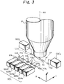
- Fig. 1 The focus detection systems GDL, GDR, and GDC shown in Fig. 1 are disposed as illustrated in Fig. 3, for example.
- Fig. 3 is a perspective view showing the disposition of detection points of the focus detection systems on the plane on which the circular image field CP of the projection lens PL on the image side is formed.
- Fig. 3 shows only the disposition of the focus detection systems GDL and GDC.
- the focus detection system GDR is omitted since it has the same configuration as the detection system GDL.
- the focus detection system GDC has two detectors GDC1 and GDC2 which are set so that detection points (detection areas) FC1 and FC2 are positioned on an extension line LLc of the axis of the strip-like of rectangular projected image SI extending in the circular field CP of the projection lens PL in a diametrical direction (X- direction).
- These detectors GDC1 and GDC2 detect the height position of the upper surface of the wafer W (or auxiliary plate portion HRS) or a positioning error amount in the Z-direction with respect to the best focus plane position.
- the focus detection system GDL includes in the embodiment five detectors GDA1, GDA2, GDB1, GBD2, and GDB3 having respective detection points (detection areas) FA1, FA2, FB1, FB2, and FB3 positioned on a straight line LLa parallel to the extension line LLc.
- Each of these five detectors independently detects the height position of a point on the upper surface of the wafer W (or auxiliary plate portion HRS) or a positioning error amount in the Z-direction with respect to the best focus plane position.
- the extension line LLc and the straight line LLa are set at a certain distance from each other in the scanning direction (Y-direction). Also, the detection point FA1 of the detector GDA1 and the detection point FC1 of the detector GDC1 are set at substantially the same coordinate positions in the X-direction while the detection point FA2 of the detector GDA2 and the detection point FC2 of the detector GDC2 are set at substantially the same coordinate positions in the X-direction.
- the detection points FB1, FB2, and FB3 of three detectors GDB1, GDB2, and GDB3 are disposed so as to cover the area of the strip-like or rectangular projected image SI in the X- direction. That is, the detection point FB2 is disposed at a X-coordinate position corresponding to the center (the point at which the optical axis AX passes) of the area of the projected image SI in the X-direction while the detection points FB1 and FB3 are disposed at X-coordinate positions corresponding to positions in the vicinity of the opposite ends of the projected image SI area in the X-direction. Therefore, the three detection points FB1, FB2, and FB3 are used for focus error pre-reading of the surface portion of the wafer W corresponding to the projected image SI area.
- the focus detection system GDR also has three pre-reading detectors GDE1, GDE2, GDE3 and other two detectors GDD1 and GDD2 disposed opposite sides of these pre-reading detectors in the X-direction.
- pre-reading detectors GDE1, GDE2, GDE3 and other two detectors GDD1 and GDD2 disposed opposite sides of these pre-reading detectors in the X-direction.
- the planes recognized as best focus positions by the twelve detectors GDA1, GDA2; GDB1, GDB2, GDB3; GDC1, GDC2; GDD1, GDD2; GDE1, GDE2, GDE3 are adjusted to one XY-plane.
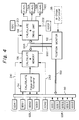
- Fig. 4 is a block diagram of an example of the AF control unit 38 for processing detection signals (error signals) from the focus detection systems GDL, GDR, and GDC shown in Figs. 1 and 3.
- one of the group of detection signals from the five detectors GDA1, GDA2, GDB1, GDB2, and GDB3 of the pre-reading focus detection systems GDL and the group of detection signals from the five detectors GDD1, GDD2, GDEI, GDE2, and GDE3 of the focus detection systems GDR are selected by a changeover circuit 50 to be supplied to subsequent processing circuits.
- the changeover circuit 50 selects the signals from one of the focus detection systems GDL and GDR in response to a changeover signal SST (representing a direction discrimination result) supplied from a position monitor circuit 52 which discriminates one scanning movement direction of the wafer stage 34 from the other on the basis of stage control information from the wafer stage controller 35, and which monitors changes in the moved position of the wafer W from the pre- read position to the exposure position.
- SST a changeover signal supplied from a position monitor circuit 52 which discriminates one scanning movement direction of the wafer stage 34 from the other on the basis of stage control information from the wafer stage controller 35, and which monitors changes in the moved position of the wafer W from the pre- read position to the exposure position.
- the changeover circuit 50 is selecting the five detection signals from the focus detection system GDL.
- the detectors GDA1 and GDA2 supplies the second calculation and memory circuit 56 with information ZA1 and information ZA2 representing the surface height positions (or focus deviations) at the detection points FA1 and FA2 simultaneously with the detection of the wafer surface by the three detectors GDB1, GBD2, and GDB3.
- the second calculation and memory circuit 56 calculates, on the basis of error data DT1, DT2, information ZA1, ZA2 and the relative positional relationship between the detectors, target values ⁇ Z1 and ⁇ Z2 of the height position of the wafer W which should be detected at the detection points FC1 and FC2 of the detectors GDC1 and GDC2 set at the projection exposure position with respect to the Y-direction (scanning direction).
- the second calculation and memory circuit 56 temporarily stores the calculated target values ⁇ Z1 and ⁇ Z2.
- the meaning of the target values ⁇ Z1 and ⁇ Z2 is that, if information ZC1 and information ZC2 detected by the detectors GDC1 and GDC2 when the surface portions of the wafer W (or auxiliary plate portion HRS) previously read at the pre- reading detection points FA1 and FA2 reach the detection points FC1 and FC2 corresponding to the exposure position are equal to the target values ⁇ Z1 and ⁇ Z2, respectively, both the focus error amount ⁇ Zf and tilt error amount ⁇ Tx determined by pre-reading become zero at the exposure position.
- the second calculation and memory circuit 56 outputs the stored target values ⁇ Z1 and ⁇ Z2 to a third calculation and drive circuit 58 immediately before the pre-read area on the wafer with respect to the Y-direction arrives at the exposure position at which the projected image SI is exposed.
- the second calculation and memory circuit 56 outputs signals representing target values ⁇ Z1 and ⁇ Z2 temporarily stored to the third calculation and drive circuit 58 after delaying the signals by an amount of time determined by the distance between the straight line LLa and the extension line LLc in the Y-direction and the speed of movement of the wafer W.
- a certain number of sets of target values ⁇ Z1 and ⁇ Z2 e.g., five sets
- a certain number of sets of target values ⁇ Z1 and ⁇ Z2 e.g., five sets
- a certain number of sets of target values ⁇ Z1 and ⁇ Z2 e.g., five sets
- a number obtained by dividing the distance between the straight line LLa and the extension line LLc in the Y-direction e.g., about 40 mm
- the width of the projected image SI e.g., about 8 mm
- the second calculation and memory circuit 56 functions as a memory for storing target values ⁇ Z1 and ⁇ Z2 in a first in-first out (FIFO) manner.
- the third calculation and drive circuit 58 reads, in response to a signal SS3 from the position monitor circuit 52, detection information ZC1 and ZC2 on the height position of the surface of the wafer W (or auxiliary plate portion HRS) detected by the detectors GDC1 and GDC2 immediately before the area on the wafer W detected at the pre-read position reaches the exposure position (the position of the projected image SI).
- the third calculation and drive circuit 58 reads the data of target values ⁇ Z1 and ⁇ Z2 (corresponding to the exposure position) output from the second calculation and memory circuit 56, determines, by calculation, drive amounts (amounts of position adjustment or amounts of speed adjustment) corresponding to the Z-drive motors 32A, 32B, and 32C shown in Fig. 1 on the basis of information ZC1 and ZC2 and target values ⁇ Z1 and ⁇ Z2, and outputs determined drive amount data to the Z-drive motors 32A, 32B, and 32C.
- Fig. 4 may be embodied in a programmed microcontroller or microprocessor, executing a suitable program which could be written by one of ordinary skill in the art in light of Fig. 4.
- Fig. 5 is a plan view explaining the function of the auxiliary plate portion HRS formed at the peripheral portion of the wafer holder WH as shown in Fig. 1.
- Fig. 5 is a plan view explaining the function of the auxiliary plate portion HRS formed at the peripheral portion of the wafer holder WH as shown in Fig. 1.
- all the detection points of the focus detection systems are positioned outside the projection field CP of the projection lens PL as described above, there is a possibility of some of the focus detection points being located outside the perimeter of wafer W at the time of scanning exposure of some of a plurality of shot areas SAn on the wafer arranged at the peripheral portion of the wafer W.
- the end focus detection point FA1 (or FD1) of the pre-reading focus detection system GDL (or GDR) and the detection point FC1 of the exposure position focus detection system GDC are located outside the wafer W. In this state, it is difficult to normally perform focusing and tilt adjustment.
- a main function of the auxiliary plate portion HRS is enabling normal focusing and tiling in such a situation.
- the detection point FA1 (or FD1) and the detection point FC1 located outside the of the wafer W are set so as to be positioned on the surface of the auxiliary plate portion HRS. Accordingly, it is desirable that the height of the surface of the auxiliary plate portion HRS is substantially equal to that of the surface of the wafer W.
- the surface of the wafer W and the surface of the auxiliary plate portion HRS are made flush with each other within the detection ranges which correspond to the detection points FA1 (FA2), FC1 (FC2), and FD1 (FD2) and in which the desired linearity of the focus detectors corresponding to the detection points are ensured.
- the surface of the auxiliary plate portion HRS is used as an alternative to the surface of the wafer W, its reflectivity is set on the same order or to the same value as the reflectivity of a standard (silicon) wafer.
- a mirror-finished surface is preferred as the auxiliary plate portion HRS.
- the detection points FA1, FA2; FB1, FB2, FB3 of the focus detection system GDL are selected as pre-reading sensors with respect to the shot area SA1.
- the distance between the extension line LLc corresponding to the center of the projected image SI in the Y-direction and the straight line LLa on which the detection points of the focus detection system GDL are disposed is DLa and if the distance between the extension line LLc and the straight line LLb on which the detection points of the other focus detection system GDR are disposed is DLb, DLa and Dlb are set so that DLa is approximately equal to DLb in this embodiment.
- Fig. 6A schematically shows a state of the upper surfaces of the wafer W and the auxiliary plate portion HRS detected by the pre-reading focus detection system GDL at an instant during scanning exposure of the peripheral shot area SA1 of the wafer W as shown in Fig. 5.
- a horizontal line BFP represents the optimum focus plane of the projection lens PL.
- the detector GDB1 that detects the position of the wafer surface in the Z-direction at the focus detection point FB1 in the shot area SA1 outputs a detection signal representing ⁇ ZB1 as a Z- position error (amount of defocusing) of the wafer surface with respect to the plane BFP.
- the detectors GDB2 and GDB3 that detect errors of the position of the wafer surface in the Z-direction at the focus detection points FB2 and FB3 output detection signals representing errors ⁇ ZB2 and ⁇ ZB3.
- Each of these Z-position errors has a negative value if the wafer surface is lower than the best focus plane BFP, or has a positive value if the wafer surface is higher than the best focus plane BFP.
- the detectors GDA1 and GDA2 simultaneously detect Z-position errors ⁇ ZA1 and ⁇ ZA2 of the wafer surface or the surface of the auxiliary plate portion HRS with respect to the best focus plane at the detection points FA1 and FA2. These errors ⁇ ZA1, ⁇ ZA2 are temporarily stored in the second calculation and memory circuit 56.
- the second calculation and memory circuit 56 calculates the Z-position target value ⁇ Z1 to be detected at the detection point FA1 and the Z-position target value ⁇ Z2 to be detected at the detection point FA2 on the basis of data DT1 and DT2 (error amount ⁇ Zf and ⁇ Tx), Z-position errors ⁇ ZA1, ⁇ ZA2 actually measured at the detection points FA1 and FA2 and the distance DS between the middle point of the shot area and each of the detection points FA1 and FA2 in the X-direction.
- the calculated Z-position target values ⁇ Z1 and ⁇ Z2 are temporarily stored in the second calculation and memory circuit 56 until the pre-read area on the wafer W reaches
- the third calculation and drive circuit 58 shown in Fig. 4 reads the detection signals from the focus detectors GDC1 and GDC2 for detecting Z-position errors at the detection points FC1 and FC2. If, for example, the pre-read area on the wafer W is in a state such as shown in Fig. 6D immediately before it reaches the exposure position, the detector GDC1 outputs detection signal ZC1 representing a Z-position error at the detection point FC1 while the detector GDC2 outputs detection signal ZC2 representing a Z-position error at the detection point FC2.
- the third calculation and drive circuit 58 calculates the drive amounts for the three Z-actuators 32A, 32B, and 32C necessary for tilting the wafer holder WH and/or translating the wafer holder WH in the Z-direction so that the values of detection signals ZC1 and ZC2 supplied from the detectors GDC1 and GDC2 become respectively equal to the Z-position target values ⁇ Z1 and ⁇ Z2 which are supplied from the second calculation and memory circuit 56 by being delayed.
- the third calculation and drive circuit 58 supplies the Z-actuators 32A, 32B, 32C with signals corresponding to the calculated drive amounts.
- the shot area SA1 of the upper surface of wafer W is thereby precisely adjusted to coincide with the best focus plane BFP at the exposure position.
- the projected image SI of the pattern of the reticle R to be maintained in an optimal imaged state is exposed in the scanning mode of the shot area.
- each detector in the pre-reading focus detection system GDL and each detector in the exposure position focus detection system GDC are set (calibrated) so as to output a detection signal indicating that there is no focus error when the surfaces of the wafer W or the auxiliary plate portion HRS coincide with the best focus plane BFP.
- a detection offset between the detectors GDA1 and GDA2 (GDD1 and GDD2) in the pre-reading focus detection system GDL (GDR) and the exposure position focus detectors GDC1 and GDC2 steadily defocuses the pattern image formed on the wafer W for exposure.
- an offset value between the height position in the Z-direction at which the detector GDC1 detects the zero focus error and the height position in the Z-direction at which the detector GDA1 (GDD1) detects the zero focus error may be measured and stored by simultaneously performing focus detection by these detectors on the extremely high flatness surface of a reflective glass plate (or fiducial plate) provided on the wafer holder WH.
- This surface may be structure HRS or another structure separate from structure HRS.
- the correction by the stored offset value may be made when the Z-actuators 32A, 32B, and 32C are drive on the basis of the Z-position errors detected by the exposure position focus detectors GDC1 and GDC2.
- a focus and tilt sensor in accordance with a second embodiment of the present invention is next described with reference to Figs. 7A and 7B.
- the second embodiment a situation is supposed in which the projected image SI contained in the circular field of the projection lens PL has a comparatively large maximum width in the Y-direction (scanning direction) such that the influence of a tilt of the surface of wafer W in the Y-direction, i.e., pitching, is considerable.
- an exposure position focus detector GDC1 (not illustrated) is provided which has two detection points FCla and FClb disposed symmetrically about extension line LLc in the Y-direction above the projected image SI
- another exposure position focus detector GDC2 (not illustrated) is provided which has two detection points FC2a and FC2b disposed symmetrically about extension line LLc in the Y-direction below the projected image SI.
- a pre-reading focus detector GDA1 having two detection points FAla and FAlb disposed symmetrically about straight line LLa in the Y-direction and a pre-reading focus detector GDA2 (not illustrated) having two detection points FA2a and FA2b disposed symmetrically about straight line LLa in the Y- direction are provided.
- a pre-reading focus detector GDD1 (not illustrated) having two detection points FD1a and FD1b disposed symmetrically about straight line LLb in the Y-direction and a pre-reading focus detector GDD2 having two detection points FD2a and FD2b disposed symmetrically about straight line LLb in the Y-direction are provided.
- the focus detection system shown in Fig. 7A reproduces adjustment amounts (i.e., target values ⁇ Z1 and ⁇ Z2) necessary for correcting the pre-read surface configuration (i.e., error amount ⁇ Zf and ⁇ Tx) of each shot area at the detection points of the off-axis detectors GDC1 and GDC2 in the same manner as the above-described first embodiment, thereby enabling focus adjustment in the Z-direction and tilt adjustment in the X-direction (rolling direction) of the exposure area.
- adjustment amounts i.e., target values ⁇ Z1 and ⁇ Z2
- the pre-reading focus detection system GDL (GDR) and the exposure position focus detection system GDC have pairs of detection points (FAna and FAnb; FBna and FBnb; FCna and FCnb; FDna and FDnb; FEna and FEnb) spaced apart by a certain distance in the Y-direction, a tilt error amount ⁇ Ty of the pre-read shot area in the pitching direction can be detected from the differences between Z-position errors at the detection points (... na, ...
- nb forming pairs in the Y-direction, and adjustment amounts (i.e., target values ⁇ ZA1, ⁇ ZA2) necessary for correcting the surface configuration of the shot area including of the tilt error amount ⁇ Ty, can be reproduced at the detection points (FCna and FCnb) of the off-axis detectors GDC1 and GDC2.
- adjustment amounts i.e., target values ⁇ ZA1, ⁇ ZA2 necessary for correcting the surface configuration of the shot area including of the tilt error amount ⁇ Ty
- the detectors GDB1, GDB2, and GDB3 for detecting the focus positions at the detection positions FB1, FB2, and FB3 shown in Fig. 3 are disposed as systems independent of each other by being fixed to a lower portion of the projection lens PL. However, at least these three detectors GDB1, GDB2, and GDB3 may be arranged to detect the focus positions at the detection points FB1, FB2, and FB3 through a common objective lens system. The same can also be said with respect to the group of three detectors GDE1, GDE2, and GDE3 for detecting the focus positions at the detection points FE1, FE2, and FE3 shown in Fig. 5.
- An arrangement of using a common objective lens system for detectors for detecting the focus positions at a plurality of detection points is therefore described briefly with reference to Fig. 7B.
- the focus positions at these ten points are detected through the objective lens system.
- illumination light ILF from an illumination optical system 80A including a light source e.g. a light emitting diode, a laser diode, a halogen lamp or the like
- a light source e.g. a light emitting diode, a laser diode, a halogen lamp or the like
- Light transmitted through the small slits is incident upon an objective lens 84A of a projection system via a lens system 82A and a reflecting mirror 83A and is deflected by a prism 85A by a desired angle to form a slit image at each detection point.
- the illumination optical system 80A, the multi-slit plate 81A, the lens system 82A, the reflecting mirror 83A, the objective lens 84A and the prism 85A constitute a projection system of an oblique incident light type focus detection unit.
- the solid lines in the optical path from the multi-slit.plate 81A to the wafer W shown in Fig. 7B represent principal rays of transmitted light from the small slits, and the broken lines in the optical path represent typical imaging rays SLf of the small slit imaging light imaged at the detection point FB2a (or FB2b).
- the reflected light of the small slit imaging light reflected at each detection point on the wafer W is again imaged on a receiving slit plate 81B via a prism 85B, an objective lens 84B, a reflecting mirror 83B and a lens system 82B disposed generally symmetrically with respect to the projection system.
- Ten small receiving slits disposed in correspondence with the small slits in the projection multi- slit plate 81A are formed in the receiving slit plate 81B.
- Light transmitted through these receiving slits is received by a light receiving device 80B which is a plurality of photoelectric detection elements.
- the photoelectric detection elements of the light receiving device 80B As the photoelectric detection elements of the light receiving device 80B, ten photoelectric detection elements are provided in correspondence with the positions of the small slits of the receiving slit plate 81B to separately detect the focus positions at the detection points on the wafer.
- the light receiving device 80B, the receiving slit plate 81B, the lens system 82B, the reflecting mirror 83B, the objective lens 84B and the prism 85B constitute a light receiving system of the oblique incident light type focus detection unit.
- the projection system and the receiving system shown in Fig. 7B are mounted on an integrally-formed metal member so that the positions of the components are accurately maintain- ed relative to each other.
- the metal member is rigidly fixed on the lens barrel of the projection lens PL.
- oblique incident light type focus detection units each having a projection system and a receiving system arranged in the Y-direction of Fig. 7A (direction perpendicular to paper in Fig. 7B) may be provided on the opposite sides of the projection lens PL in the X-direction. Also in the case where the focus position detection points are disposed as shown in Fig. 5, the oblique incident light type focus detection unit shown in Fig. 7B can also be applied in the same manner.
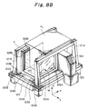
- a scanning aligner to which the present automatic focusing/tilt control system is applied is next described in accordance with a third embodiment of the present invention with reference to Fig. 8A.
- This embodiment is applicable to a scanning aligner for a large substrate e.g. 300 mm diameter or greater having a 1X projection optical system formed of a tandem combination of a first-stage Dyson type (catadioptric) projection imaging system consisting of a pair of prism mirrors PM1 and PM2, a lens system PL1 and a concave mirror MR1 and a second-stage Dyson type projection imaging system consisting of a pair of prism mirrors PM3 and PM4, a lens system PL2 and a concave mirror MR2.
- a first-stage Dyson type (catadioptric) projection imaging system consisting of a pair of prism mirrors PM1 and PM2, a lens system PL1 and a concave mirror MR1 and a second-stage Dyson type projection imaging system consisting of a
- a mask M provided as an original plate and a plate P provided as a photosensitive substrate are integrally supported on a carriage 100, and a pattern on the mask M is transferred onto the plate P as a 1X (unit magnification) erect image by moving the carriage 100 to the left or right as viewed in Fig. 8A relative to the projection field of the 1X projection optical system and illumination light IL so as to scan the mask M and plate P.
- a 1X unit magnification
- the projection optical system for this type of aligner it is desirable to minimize the spacing between the incidence plane of the prism mirror PM1 and the surface of the mask M and the spacing between the exit plane of the prism mirror PM4 and the upper surface of the plate P for reducing deteriorations in imaging performance (various aberrations and image distortion) .
- these spacings can be sufficiently reduced, the design of the lens systems PL1 and PL2 disposed on the optical axes AX1 and AX2 becomes easier. Therefore, to achieve the desired imaging performance, it is necessary to reduce the spacing between the prism mirror PM1 and the mask M and the spacing between the prism mirrors PM4 and the plate P.
- prereading focus detection systems GDL and GDR and an exposure position off-axis type focus detection system GDC such as those of the first embodiment (Fig. 3) or the second embodiment (Figs. 7A, 7B) are provided around the prism mirror PM4 as shown in Fig. 8A to precisely coincide the surface of the plate P and the best focus plane BFP at the exposure position immediately below the prism mirror PM4, by slightly moving the plate P in the Z-direction and the tilting direction.
- pre-reading focus detection systems GDL' and GDR' and an exposure position off-axis type focus detection system GDC' may be disposed around the prism mirror PM1 on the mask M side so as to face the mask M, as shown in Fig. 8A.
- These focus detection systems make it possible to detect a focus error and a tilt error of the area of the mask M irradiated with illumination light IL with respect to the prism mirror PM1 and to measure, in real time, a small deviation in the Z-direction (a focus shift of the image plane) and a tilt deviation (inclination of the image plane) of the best focus plane (i.e., a conjugate plane of reticle R) formed at a predetermined working distance from the prism mirror PM4.
- the image plane on which the pattern of the mask M is projected and imaged in an optimal condition by the projection optical system and the surface of the plate P can be adjusted to coincide with each other highly accurately during scanning exposure.
- FIG. 8A may be constructed so that mask M and plate P stand vertically.
- FIG. 8B is a perspective view of an exemplary structure of a scanning aligner having a vertical carriage for vertically holding mask M and plate P and for integrally moving mask M and plate P with respect to a projection optical system for scanning.
- a scanning aligner having mask M and plate P held vertically in this manner is disclosed in Japanese Laid-Open Patent Application No. (Hei) 8-162401, for example.
- the entirety of the vertical type scanning aligner is constructed on a fixed base 120A which is placed on a floor with vibration isolators interposed between four corner portions of the fixed base 120A and the floor.
- Side frame portions 121A and 121B are provided on opposite side portions of the fixed base 120A so as to stand vertically (in the X-direction).
- a mask M is placed inside the side frame portion 121A while a plate P is placed inside the side frame portion 121B.
- an opening is formed in which an end portion of an illumination unit 122 having optical systems for illuminating mask M with exposure illumination light and for mask-plate alignment is inserted, as illustrated.
- a guide base portion 123 is provided on the fixed base 120A so as to extend in the scanning direction (Y-direction). Between the side frame portions 121A and 121B. Two straight guide rails 123A and 123B are formed on the guide base portion 123 so as to extend in the Y-direction parallel to each other.
- a vertical carriage 125 is supported by fluid bearings or magnetic floating bearings on the guide rails 123A and 123B reciprocatingly movably in the Y-direction. The vertical carriage 125 is driven in the Y-direction in a non-contact manner by two parallel linear motors 124A and 124B having stators fixed on the guide base portion 123.
- the vertical carriage 125 has a mask-side carriage portion 125A vertically formed inside the side frame portion 121A to hold mask M and a plate-side carriage portion 125B vertically formed inside the side frame portion 121B to hold plate P.
- a mask table 126A for slightly moving mask M in the X- or Y- direction in an XY-plane or in a rotational ( ⁇ ) direction and for slightly moving mask M in the Z-direction while holding mask M is provided on the mask-side carriage portion 125A.
- a plate stage 126B for slightly moving plate P in the X- or Y-direction in an XY-plane or in a rotational ( ⁇ ) direction and for slightly moving plate P in the Z-direction while holding plate P is provided on the plate-side carriage portion 125B.
- a projection optical system PL such as one disclosed in Japanese Laid-Open Patent Application No. (Hei)8-162401 mentioned above is used in this embodiment.
- the projection optical system PL is constructed by arranging a plurality of sets (e.g., seven sets) of "1X" erect type double Dyson systems in the direction perpendicular to the X-direction.
- the plurality of sets of double Dyson systems are integrally combined and housed in a casing which is generally T-shaped as viewed in an XZ-plane.
- the projection optical system PL thus constructed is mounted by being suspended from upper end portions of the opposite side frame portions 121A and 121B so that predetermined working distances from mask M and plate P are maintained.
- mask M-side focus detection systems GDC', GDL', and GDR' on the mask M side and plate P-side focus detection systems GDC, GDL, and GDR on the plate P side are provided so as to face mask M and plate P, respectively, as shown in Fig. 8A.
- the detection points defined by the pre-reading focus detection systems GDL, GDL', GDR, and GDR' may be set in correspondence with the projection fields of the plurality of sets of double Dyson systems or may be arranged at predetermined intervals irrespective of the placement of the projection fields.
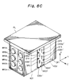
- Fig. 8C is a perspective view of an example of a layout of detectors in mask M-side focus detection systems GDC', GDL', and GDR' provided in the casing of the projection optical system PL shown in Fig. 8B.
- the effective projection fields DF1, DF2, DF3, DF4, DF5, ... of the plurality of sets of double Dyson systems are set as trapezoidal areas elongated in the X-direction perpendicular to the scanning direction.
- the projection fields DFn on the mask M side are illustrated in Fig. 8C, the projection fields on the plate P side are also arranged in the same manner.
- the projection field DF2 shown in Fig. 8C is defined by a double Dyson system such as that shown in Fig. 8A including two concave mirrors MR2a and MR2b
- the projection field DF4 is defined by a double Dyson system including two concave mirrors MR4a and MR4b.
- detectors GDA1', GDB1', GDB2' ..., GDA2' (detectors GDA2' not being seen in Fig. 8C) for the pre-reading focus detection system GDL' and detectors GDD1', GDE1', GDE2' ..., GDD2' (detectors GDD2' not being seen in Fig. 8C) for the pre-reading focus detection system GDR' are disposed on the opposite sides (on the front and rear sides with respect to the scanning direction) of the plurality of projection fields DFn. Also, exposure position focus detectors GDC1' and GDC2' (detector GDC2' not being seen in Fig. 8C) are disposed at the opposite ends of the entire array of the plurality of projection fields DFn in the X-direction perpendicular to the scanning direction.
- Each of the focus detectors described above is e.g. an air micrometer type electrostatic gap sensor. They may alternatively be oblique incident light type focus detectors. While only the focus detectors for detection on the mask M side are illustrated in Fig. 8C, a plurality of detectors are also arranged in the same manner in the focus detection systems GDC, GDL, and GDR for detection of the plate P.
- Adjustment portions KD1 and KD2 for adjusting various optical characteristics of the plurality of sets of double Dyson systems are provided on side portions of the casing of the projection optical system PL shown in Fig. 8C. Therefore, a mechanism is provided to adjust the Z-direction position, i.e., to set a mechanical (optical) focus offset detected as a best focus plane by each focus detector, if the position of the best focus plane on the mask M side or plate P side is changed in the Z-direction in Fig. 8C by the optical characteristic adjustment.
- This mechanism may be e.g. a mechanism which mechanically adjusts the position of a focus detector in the Z direction, or a mechanism which optically adjusts the position recognized as the best focus position by the focus detector in the Z direction, so that the optical path length is changed optically.
- the mask or plate are automatically adjusted for focusing in the Z direction according to detection signals which represent a focus error, and an offset is added to its moved position in the Z direction.
- FIG. 9 is a cross-sectional view of a portion of the apparatus from the end of the projection lens system PL and to a wafer holder WH.
- a positive lens element LE1 having a flat lower surface Pe and a convex upper surface is fixed on the end of the projection lens system PL inside the lens barrel.
- the lower surface Pe of this lens element LE1 is finished so as to be flush with the end surface of the extreme end of the lens barrel, so that a flow of a liquid LQ is disturbed only to a minimal extent.
- detectors of pre-reading focus detection systems GDL and GDR and an exposure position focus detection system GDC which are similar to those shown in Fig. 1 are attached so that their extreme end portions are immersed in liquid LQ.
- a plurality of attraction surfaces 113 for attracting the reverse surface of wafer W by vacuum suction are formed in a central inner bottom portion of the wafer holder WH. More specifically, the attraction surfaces, 113 have a plurality of circular-band-like land portions which have a height of about 1 mm and which are formed concentrically with each other with a predetermined pitch in the diametrical direction of the wafer W. Each of the grooves formed in central portions of the circular land portions communicates with a tubing 112 in the wafer holder WH. The piping 112 is connected to a vacuum source for vacuum suction.
- the spacing (substantial working distance) between the lower surface Pe of the lens element LE1 at the end of the projection lens system PL and the upper surface of the wafer W (or auxiliary plate portion HRS) in an optimum focus state i.e., the thickness of liquid LQ in which a projection optical path is formed, is set to be 5 mm or less. Accordingly, the depth Hq of liquid LQ filling the wafer holder WH may be two to several times larger than this thickness (5mm or less), and the height of a wall portion LB vertically formed at the peripheral end of the wafer holder WH is about 10 to 25 mm.
- the thickness of liquid LQ in the imaging optical path corresponding to the working distance of the projection lens system PL is reduced, so that the total volume of liquid LQ filling the wafer holder WH is smaller and hence temperature control of the liquid [LQ] is easier.
- Fig. 10 shows the construction of a focus detection system GDL disposed in the vicinity of a projection lens system PL.
- Other detection systems GDR and GDC are constructed in the same manner as the detection system GDL.
- the same components as those shown in Fig. 9 are indicated by the same reference characters or numerals.
- a prism mirror 200 formed of a glass block and having a lower portion immersed in liquid LQ is fixed in the vicinity of a peripheral portion of the projection lens system PL.
- the prism mirror 200 has reflecting surfaces 200a and 200b partially immersed in liquid LQ, and flat surfaces 200c and 200d through which the projected beam or reflected beam travels out of the glass of the prism mirror 200 into liquid LQ or out of liquid LQ into the glass. Also the prism mirror 200 has a flat upper surface.
- a multi-slit plate 205 is illuminated through a condenser lens or a cylindrical lens 203 with light LK (having a non-actinic wavelength relative the resist on wafer W) from a light source 202 such as a light emitting diode (LED) or a laser diode (LD) for forming a projected beam for focus/tilt detection.
- a light source 202 such as a light emitting diode (LED) or a laser diode (LD) for forming a projected beam for focus/tilt detection.
- a plurality of transmission slits corresponding to detection points (areas) FAn and F3n of the focus detection system GDL are formed in the slit plate 205.
- the light from each transmission slit is reflected by a beam splitter 207 and is incident upon an objective lens 209 to be converged as an imaging beam forming a slit image on the upper surface of wafer W.
- the imaging beam emergent from the objective lens 209 enters the prism mirror 200 through the upper end surface of the same, is normally reflected by the reflecting surface 200a, and enters liquid LQ through the flat surface 200c to be obliquely incident upon the surface of wafer W to irradiate the same.
- the beam reflected by wafer W enters the prism mirror 200 through the opposite flat surface 200d, is normally reflected by the reflecting surface 200b and travels out of the prism mirror 200 through the upper end surface.
- This reflected light beam passes through an objective lens 211 and is reflected by a reflecting mirror 213 disposed at a pupil position of the objective lens 211.
- the beam reflected by the mirror 213 travels reversely through the objective lens 211 and again travels via the reflecting surface 200 and the flat surface 200d of the prism mirror 200 to again irradiate wafer W.
- the light beam again reflected by wafer W travels via the flat surface 200c and the reflecting surface 200a of the prism mirror 200, passes the beam splitter 207 and is incident on a photoelectric detector 215.
- the photoelectric detector 215 is a plurality of light receiving elements corresponding to the slits of the slit plate 205.
- the photoelectric detector 215 separately outputs detection signals with respect to the detection points FAn and FBn, respectively.
- the focus/tilt detection system shown in Fig. 10 is arranged as a double-path system in which the projected beam reflected by wafer W is again reflected by wafer W, and can therefore have higher sensitivity for detection of an error in the wafer W surface position in the Z-direction in comparison with a single-path system.
- a glass block (prism mirror 200) is provided at the extreme end of the focus/tilt detection system and is positioned so as to be partially immersed in liquid LQ, so that the projected beam and the reflected beam do not pass any interface between liquid LQ and air, thus providing a stable beam path.
- the effective length of the path in liquid LQ through which the projected beam or reflected beam travels is reduced by virtue of the prism mirror 200, thereby avoiding any reduction in accuracy due to temperature variation of liquid LQ at the time of Z-position measurement.
- this Z-drive unit 220 is used to correct the height of surface of the auxiliary plate HRS so that the difference is reduced to a value smaller than the allowable value.
- the surface of the auxiliary plate HRS functions as an alternative detection surface for the focus detection points FA1 (or FA2), FC1 (or FC2), and FD1 (or FD2) located outside wafer W when shot area SA1 at the peripheral portion of wafer W is exposed.
- the focus detectors GDA1, GDA2, GDC1, GDC2, GDD1, and GDD2 having detection points each of which is not exclusively positioned on one of the surface of the auxiliary plate HRS and the surface of wafer W must accurately measure the Z-position on each of these surfaces. That is, it is necessary for the positions in the Z-direction of the surfaces of the auxiliary plate HRS and wafer W to be within the linear focus measuring range of the each focus detectors GDAn, GDCn and GDDn.
- the linear focus measuring range of the focus detectors is ⁇ 10 micrometers
- the Z positional deviations of the surfaces of the auxiliary plate HRS and wafer W are limited within the range of several micrometers.
- the thickness of wafers varies in a tolerance determined by the SEMI standard, and it is difficult to limit the thicknesses of all usable wafers within the range of several micro-meters.
- the difference between the Z-position of a suitable portion of the wafer W surface (e.g., a central portion of a peripheral shot area) and the Z-position of the surface of the auxiliary plate HRS is measured by using one of the focus detection systems (GDL, GRD, GDC) before exposure. If the difference exceeds the allowable range (e.g., several micro-meters), the height of the auxiliary plate HRS is adjusted so that the difference is within the allowable range by controlling the fine Z-drive units 220 shown in Fig. 11A. Since the wafer holder WH shown in Fig. 11A is filled with liquid LQ, the fine Z-drive units 220 are "waterproofed" to prevent the liquid from entering the units.
- the allowable range e.g., several micro-meters
- Fig. 11B is a cross-sectional view of a modified example of the structure including a wafer holder WH and a ZL stage 30, which is suitable for exposure of a wafer in air.
- the components corresponding to those shown in Fig. 11A are indicated by the same reference characters or numerals.
- the wafer holder WH is constructed as a chuck on which only an attraction surface 113 for supporting wafer W is formed, and which is fixed on a ZL stage 30.
- An auxiliary plate HRS is mounted on the ZL stage 30 with fine Z-drive units 220 interposed therebetween.
- Each function point PV of three Z-actuators 32A, 32C, and 32B (32B not being seen in Fig. 11B) for driving the ZL state 30 in the Z- direction and a tilting direction are set to points at a peripheral portion of the ZL stage 30 substantially at the same height as the wafer mount surface (attraction surface 113) of the wafer holder WH.
- the height of the auxiliary plate HRS is adjusted to that of the upper surface of wafer W by using fine Z-drive units 220 in the same manner as shown in Fig. 11A.
- This structure of the ZL stage 30 and the Z-actuators 32A, 32C, and 32B shown in Fig. 11B, in which the height of the function points PV are set to the same level as the wafer surface, may also be applied to the aligner shown in Fig. 1.
- the wafer holder WH of Fig. 11A may be mounted on the ZL stage 30 of Fig. 11B to form a focusing and tilting stage suitable for immersion projection exposure apparatus or its method.
- the focus detection systems GDL, GDR, and GDC may include electrostatic capacity type gap sensors or air micrometer type gap sensors in the case of an aligner for performing projection exposure in air.
- the present invention is applicable e.g. to any of the step-and-repeat type, step-and-scan type and "1X" scanning type projection aligners using, as exposure light, g-line (463 nm) or i-line (365 nm) from a mercury discharge lamp or pulse light (248 nm) from KrF excimer laser.
- precise focusing and tilt control at the exposure position can be realized while the working distance of the projection optical system mounted in the projection aligner is set to an extremely small value, so that correction of various aberrations and distortion correction in optical design of the projection optical system become easier and the transparent optical element positioned near the image plane, in particular, can be reduced in size.
- Each of the focusing/tilt control systems in accordance with the above-described embodiments of the present invention is applicable to a certain type of projection exposure apparatus.
- the present invention is also applicable to focus/tilt detection systems for beam processing (manufacturing) apparatuses, writing apparatuses, inspection apparatuses and the like and is not limited to semiconductor fabrication.
- These beam processing apparatuses, writing apparatuses and inspection apparatuses are provided with an optical or electrooptical objective system to which the present invention can be applied as a focus detection system for detecting a focus on a substrate, specimen or workpiece.
- Fig. 12A shows the construction of a focus detection system applied to an objective optical system of an apparatus for processing a workpiece with a laser or electron beam or for writing a pattern on a workpiece
- Fig. 12B shows a planar layout of detection points of the focus detection system shown in Fig. 12A.
- a processing or writing beam LBW is deflected unidimentionally or two-dimensionally by a scanning mirror 300 and travels via a lens system 301, a fixed mirror 302 and a lens system 303 to be incident upon a beam splitter 304.
- the beam LBW is reflected by the beam splitter 304 to be incident upon a high-resolution objective system 305 having a small working distance.
- the beam LBW is condensed into a small spot having a predetermined shape (e.g., a variable rectangular shape) on a workpiece WP by the objective system 305.
- the workpiece WP is attracted to and fixed on the same holder WH as that shown in Fig. 11A or 11B.
- An auxiliary plate HRS is attached integrally to the holder WH around the workpiece WP.
- the holder WH is fixed on an unillustrated XYZ- stage to be moved two-dimensionally in a horizontal direction and in a direction perpendicular to paper as viewed in Fig. 12A.
- the holder WH is also moved slightly in the vertical direction (Z-direction) for focusing.
- the apparatus shown in Fig. 12A is also provided with an optical fiber 310 for emitting illumination light for observation, alignment or aiming, a beam splitter 311 and a lens system 312 for leading the illumination light to the above-mentioned beam splitter 304, and a light receiving device (e.g. or photomultiplier, image pickup tube, CCD or the like) 314 for photoelectrically detecting reflected light, scattered and diffracted light or the like from the workpiece WP obtained through the objective system 305.
- a light receiving device e.g. or photomultiplier, image pickup tube, CCD or the like
- Pre-reading focus detection systems GDL and GDR and a processing position focus detection system GDC are provided around the objective system 305.
- Fig. 12B shows a field 305A of the objective system 305 and a planar layout of detection points of the focus detection systems disposed around the field 305A.
- the center of the field 305A is set at the origin of an XY coordinate system.
- a rectangular area in the field 305A indicates the range through which the spot of the beam LBW scans by the deflection of the beam caused by the scanning mirror 300.
- Focus detectors GDA1, GDBn, and GDA2 on the left-hand side of the field 305A of the objective system are disposed so that detection points FA1, FB1, FB2, FB3, and FA2 is set in a row parallel to the Y-axis. Also, focus detectors GDD1, GDEn, and GDD2 on the right-hand side of the field 305A are disposed so that detection points FD1, FE1, FE2, FE3, and FD2 is set in a row parallel to the Y-axis.
- a focus detector GDC1 provided above the field 305A is set so that three detection points FD1a, FD1b, and FD1c are placed on a line passing the two detection point FA1 and FD1 and parallel to the X-axis while a focus detector GDC2 provided below the field 305A is set so that three detection points FD2a, FD2b, and FD2c are placed on a line passing the two detection point FA2 and FD2 and parallel to the X-axis.
- a set of the focus detectors GDA1, GDBn and GDA2 and a set of the focus detectors GDD1, GDEn and GDD2 are selected as the focus pre-reading function while the workpiece WP moves in the X-direction.
- the focus pre-reading function is achieved by selecting a set of the focus detectors GDA1, GDC1 and GDD1 and a set of the focus detectors GDA2, GDC2 and GDD2 while the workpiece WP moves in the Y-direction.
- This embodiment is arranged so that the detection points of the focus detectors GDBn, GDC1, GDC2, and GDEn can be changed for detecting a focus of the processing position.
- one of three pairs of detection points FD1a and FD2a, detection points FD1b and FD2b, and detection points FD1c and FD2c may be selected for focus detection of the processing position while the detection points FA1, FB1, FB2, FB3, and FA2 are being used for pre-reading.
- the position of the spot of the processing or drawing light beam LBW changes in the scanning range 305B. Therefore, when for example, the light spot is positioned at the leftmost end of the scanning range 305B as seen in Fig. 12B, the two detection points FD1a and FD2a are selected for processing position focus detection. When the light spot is positioned at the rightmost end of the scanning range 305B, the two detection points FD1c and FD2c are selected for processing position focus detection.
- the holder WH shown in Fig. 12A is slightly moved in the focusing (Z) direction and in a tilting directions on the XY stage. As is a drive system and a control system for this movement, those shown in Fig. 4 can be used without being substantially modified.
- the focus detection system shown in Fig. 12A and 12B is arranged to enable pre-reading detection of the focus in each of the directions of the two-dimensional movement of workpiece WP and to enable the focus detection point for the processing position to be selected according to the position of the beam spot in the field 305A.
- the focus detection system shown in Fig. 12A and 12B is arranged to enable pre-reading detection of the focus in each of the directions of the two-dimensional movement of workpiece WP and to enable the focus detection point for the processing position to be selected according to the position of the beam spot in the field 305A.
- Fig. 13 shows an example of an apparatus for optically inspecting defects in patterns drawn on a mask or reticle for photolithography or defects in circuit patterns of a semiconductor device or liquid crystal display device formed on a substrate.
- TTL optical focus detection system entails a problem of limiting the detection sensitivity (the amount of change in detection signal with respect to an error in focusing a specimen) because of a restriction due to the numerical aperture (NA) of the objective system.
- a TTL focus detection system is formed so as to use light having a wavelength different from that of illumination light for inspection, aberration correction must be taken into consideration with respect to the wavelength ranges of inspection illumination light and focus detection illumination light in the optical design of the objective system. In such a case, the lens cannot always be designed optimally with respect to inspection illumination light.
- a specimen WP to be inspected is e.g. a mask having a pattern Pa formed on its lower surface.
- the specimen WP is supported at its peripheral end on a frame-like two-dimensionally-movable stage 331 having an opening.
- the objective lens 330 is mounted in an upward-facing state on a base member 332 for guiding movement of the stage 331.
- An enlarged image of a local area in pattern Pa is imaged on an imaging plane of an image pickup device 336 through a beam splitter 334 and a lens system 335.
- a condenser lens 338 of an illumination optical system is disposed coaxial with the axis AX of the objective lens 330. Illumination light from an optical fiber 340 travels through a condenser lens 341, an illumination field stop 342 and a lens system 343 to be incident upon the condenser lens 338, thereby irradiating the area on the specimen WP corresponding to the field of the objective 330 with a uniform illuminance.
- the focus detection systems GDC, GDL and GDR are mounted on the base member 332 together with the objective 330 so as to upwardly face the pattern Pa.
- a plurality of focus detectors (a plurality of detection points) are provided in the focus detection systems GDL and GDR provided for pre-reading, while at least one pair of focus detectors is provided in the focus detection system GDC for detection at the inspection position.
- the specimen WP on the stage 331 may be moved vertically along the optical axis AX or tilted on the basis of focus position information detected by the focus detectors by using a control circuit such as that shown in Fig. 4.
- a focus adjuster 352A or 352B for slightly moving the objective lens 330 or the lens system 335 along the optical axis AX may be provided instead of the means for vertically moving the specimen WP.
- the illumination system may be changed so that coaxial reflection illumination light is introduced through the beam splitter 334 in the direction of the arrow 350 in Fig. 13.
- the enlarged image received by the image pickup device 336 is formed by imaging reflected light from the pattern Pa.
- a spatial filter with a transmission portion having a desired shape is removably placed at the position of a Fourier transform plane formed in the optical path of the illumination optical system or in the imaging optical system to enable a bright field image or a dark field image of pattern Pa to be selectively imaged on the image pickup device 336.
Abstract
Description
Claims (27)
- A scanning exposure apparatus comprising:(a) an imaging system for projecting an image of a pattern of a mask onto a substrate at an Imaging field;(b) a scanning mechanism for moving the mask and the substrate in a scanning direction relative to said imaging system;(c) an adjusting system for adjusting a focus of the projected image on the substrate;(d) a first detection system having a detection area at a first position located outside the imaging field of said imaging system and spaced apart from the imaging field in the scanning direction, said first detection system detecting the position of a principal surface of the substrate in a Z-direction;(e) a second detection system having a detection area at a second position located outside the imaging field of said imaging system and spaced apart from said first position in a direction intersecting the scanning direction, said second detection system detecting the position of the principal surface of the substrate in the Z-direction;(f) a third detection system having a detection area at a third position located outside the imaging field of said imaging system, spaced apart from the imaging field in a direction intersecting the scanning direction and also spaced apart from said second position in the scanning direction, said third detection system detecting the position of the principal surface of the substrate in the Z-direction;(g) a calculator coupled to said first and second detection systems and calculating a deviation between the first Z-position detected by said first detection system and a target Z-position and storing the second Z-position detected by said second detection system at the time of detection by said first detection system; and(h) a controller coupled to said adjusting system and to said calculator and to said third detection system and controlling said adjusting system on the basis of the calculated deviation, the stored second Z-position and the third Z-position detected by said third detection system when the area on the substrate corresponding to the detection area of said first detection system is positioned in the imaging field of said imaging system by movement of said scanning mechanism.
- An exposure apparatus according to Claim 1, wherein said scanning mechanism includes a mask stage for holding the mask, a substrate stage for holding the substrate, and a synchronizing drive system for moving said mask stage and said substrate stage at a speed ratio corresponding to a projection magnification of said imaging system.
- An exposure apparatus according to Claim 2, wherein said substrate stage includes an attraction portion for attracting a reverse surface of the substrate, and an auxiliary plate portion surrounding the substrate at a height approximately equal to the principal surface of the substrate when the substrate is supported on said attraction portion.
- An exposure apparatus according to Claim 3, wherein said second detection system and said third detection system are arranged to detect the position of a surface of said auxiliary plate portion in the Z-direction by at least one of the detection areas when a shot area of the substrate to be exposed by the pattern of the mask is at a peripheral portion of the substrate.
- An exposure apparatus according to Claim 4, wherein each of said first, second and third detection systems generates a Z-direction positional error value of one of the principal surface of the substrate and the auxiliary plate portion relative to predetermined reference Z-positions with respect to said first, second and third detection systems.
- An exposure apparatus according to Claim 5, wherein, if the predetermined reference Z-positions with respect to said first, second and third detection systems differ from each other, the differences between the reference Z-positions are detected by a calibration.
- An exposure apparatus according to Claim 4, wherein, if the scanning direction of the substrate is a Y-direction and if a direction perpendicular to each of the Y-direction and the Z-direction is an X-direction, said first detection system includes a first focus detector of a multi-point type having a plurality of detection areas in a row along the X-direction on the substrate over a range of a size of the imaging field of said imaging system in the X-direction.
- An exposure apparatus according to Claim 7, wherein said second detection system includes a plurality of second focus detectors having detection areas on opposite sides of the row of the plurality of detection areas of said multi-point focus detector in the X-direction, each of said second focus detectors separately detecting the Z-direction position of the principal surface of one of the substrate and the auxiliary plate portion at each of the detection areas.
- An exposure apparatus according to Claim 8, wherein said third detection system includes a plurality of third focus detectors on the opposite sides of the imaging field of said imaging system in the X-direction, each of said third focus detectors separately detecting the Z-direction position of the principal surface of one of the substrate and the auxiliary plate portion at each of the detection areas.
- A projection exposure apparatus comprising:(a) an imaging system for projecting an image of a mask pattern onto a substrate at a projection field;(b) a movable stage mechanism for moving in intersecting X and Y directions to position the substrate with respect to the image of the projected mask pattern;(c) an adjusting mechanism for adjusting a focus of the projected mask pattern image on the substrate;d) a first detection system having a detection area at a first position located outside the projection field of said imaging system and spaced apart from the projection field in the Y direction, said first detection system detecting the position of a principal surface of the substrate in a Z direction;(e) a second detection system having a detection area at a second position located outside the projection field of said imaging system and spaced apart from said first position in the X direction, said second detection system detecting the position of the principal surface of the substrate in the Z direction;(f) a third detection system having a detection area at a third position located outside the projection field of said imaging system, spaced apart from the projection field in the X direction and also spaced apart from said second position in the Y direction, said third detection system detecting the position of the principal surface of the substrate in the Z direction;(g) a calculator coupled to said first and second detection systems, and calculating a deviation between the first Z-position detected by said first detection system and a target Z-position and for storing the second Z-position detected by said second detection system at the time of detection made by said first detection system; and(h) a controller coupled to said adjusting mechanism and said calculator and said third detection system, and controlling said adjusting mechanism on the basis of the calculated deviation, the stored second Z-position and the third Z-position detected by said third detection system when the area on the substrate corresponding to the detection area of said first detection system is positioned in the projection field of said imaging system by said movable stage mechanism.
- An exposure apparatus according to Claim 10, wherein said first detection system includes a plurality of first focus detectors having a plurality of detection areas in a row along the X direction in a range according to a size of the projection field of said imaging system in the X direction, each of said first focus detectors separately detecting the Z-position of the principal surface of the substrate at each of the detection areas.
- An exposure apparatus according to Claim 11, wherein said second detection system includes two second focus detectors having two detection areas placed on opposite sides of the row of the plurality of detection areas of said first detection system, each of said second focus detectors separately detecting the Z-position of the principal surface of the substrate at each of the two detection areas.
- An exposure apparatus according to Claim 12, wherein said third detection system includes two third focus detectors placed on opposite sides of the projection field of said imaging system in the X direction, each of said third focus detectors separately detecting the Z-position of the principal surface of the substrate at each of the two detection areas.
- An exposure apparatus according to Claim 13, wherein said movable stage mechanism includes a mount portion for attracting a reverse surface of the substrate and an auxiliary plate portion which surrounds the substrate at a height substantially equal to the principal surface of the substrate when the substrate is supported on said mount portion, a surface of said auxiliary plate being detected by one of said two second focus detectors and one of said two third focus detectors.
- A scanning exposure method in which a pattern of a mask is transferred onto a sensitive substrate by projecting a part of the mask pattern on the sensitive substrate through a projection system and by moving the mask and the sensitive substrate relative to a projection field of the projection system, the method comprising the steps of:(a) mounting the sensitive substrate on a holder having an auxiliary plate portion surrounding the sensitive substrate at a height substantially equal to a height of a principal surface of the sensitive substrate;(b) reading a focus error of an exposure area of the sensitive substrate on which area a part of the mask pattern is to be projected, the focus error of the exposure area being read before the exposure area reaches the projection field of the projection system during scanning movement of the holder and the sensitive substrate;(c) detecting a focus error of the principal surface of a part of one of the sensitive substrate and the auxiliary plate portion by an exposure position focus detection system disposed apart from the projection field of the projection system in a direction perpendicular to the direction of said scanning movement when the exposure area on the sensitive substrate reaches the projection field; and(d) adjusting the focus between the projection system and the sensitive substrate on the basis of the focus errors detected by said steps (b) and (c) so that the focus error of the exposure area on the sensitive substrate is corrected in the projection field of the projection system.
- A method according to Claim 15, applied to a projection aligner having a projection system having an effective working distance to the principal surface of the substrate of 20 mm or less.
- A method according to Claim 15, applied to an immersion projection exposure apparatus in which a space containing a projection optical path between the sensitive substrate and a transparent optical element disposed at an image plane side of the projection optical system is liquid filled.
- A method according to Claim 17, wherein the projection optical system has a working distance such that the thickness of the liquid between the sensitive substrate and the transparent optical element of said projection optical system is 2 mm or less.
- A method according to Claim 15, applied to a scanning exposure apparatus having a catadioptric projection system having a refractive optical material and a reflecting optical material, and in which a transparent optical element is disposed at an image plane side.
- A method according to Claim 19, wherein the transparent optical element disposed at the image plane side is a prism mirror having an emergent surface substantially parallel to the principal surface of the sensitive substrate.
- A focusing apparatus provided in an apparatus having an objective optical system to control focusing between a surface of a workpiece and the objective optical system, said focusing apparatus comprising:(a) a first detection system having a detection area at a first position located outside a field of said objective optical system, said first detection system detecting a position of the surface of the workpiece in the focusing direction;(b) a second detection system having a detection area at a second position located outside the field of said objective optical system and spaced apart from said first position, said second detection system detecting the position of the surface of the workpiece in the focusing direction;(c) a third detection system having a detection area at a third position located outside the field of said objective optical system and spaced apart from each of said first and second positions, said third detection system detecting the position of the surface of the workpiece in the focusing direction;(d) a calculator coupled to said first and second detection systems, and calculating a deviation between the first focus position detected by said first detection system and a target focus position and for storing the second focus position detected by said second detection system at the time of detection made by said first detection system; and(e) a controller coupled to said calculator and to said third detection system, and controlling focusing of the objective optical system on the surface of the workpiece on the basis of the calculated deviation, the stored second focus position and the third focus position detected by said third detection system when the area on the workpiece corresponding to the detection area of said first detection system is positioned in the field of said objective optical system by relative movement of the workpiece and the objective optical system.
- A method of controlling focusing of an objective optical system onto a surface of a workpiece when the workpiece and a field of the objective optical system are moved relative to each other in X and Y directions, said method comprising the steps of:(a) mounting the workpiece on a holder having an auxiliary plate portion surrounding the workpiece at a height substantially equal to a height of the surface of the workpiece;(b) reading a focus error of a predetermined local portion of the surface of the workpiece before the local portion of the workpiece reaches the field of the objective optical system during movement of said holder and the workpiece in a predetermined moving direction;(c) detecting a focus error of the surface of a part of one of the workpiece and the auxiliary plate portion by a first focus detection system disposed apart from the field of the objective optical system in a direction perpendicular to the moving direction when the local portion of the workpiece reaches the field; and(d) controlling the focusing between the objective optical system and the workpiece on the basis of the focus errors detected by said steps (b) and (c) so that the focus error of the local portion of the workpiece is corrected in the field of the objective optical system.
- A method according to Claim 22, applied to at least one of a manufacturing instrument, a lithography exposure apparatus, a writing apparatus and an inspection apparatus having a small effective working distance such that a detecting beam of an oblique incident light type focus detector cannot be obliquely led to the surface of the workpiece immediately below the objective optical system.
- A projection exposure apparatus for projecting a mask pattern image onto a sensitive substrate through an optical imaging system and a liquid in a space between the substrate and the imaging system, said apparatus comprising:an assembly holding a plurality of optical elements of said imaging system, wherein at least an end portion of said assembly is immersed in said liquid; anda distal optical element mounted at the end portion of said assembly and having a distal surface which confronts the substrate and contacts said liquid;wherein the distal surface of said distal optical element and a surface of the end portion of said assembly are substantially flush to each other, thereby suppressing disturbance of flowing of said liquid.
- A method for fabricating a feature on a semiconductor wafer, employing a projection system, comprising the steps of:(a) mounting the semiconductor wafer on a holder having a wall portion vertically provided at a peripheral portion to form a liquid layer on the wafer for achieving an immersed condition between a surface of the wafer and said projection system;(b) scanning said holder along an image plane of said projection system to perform a scan-exposure by projecting a feature pattern image onto the wafer through said projection system and said liquid layer; and(c) correcting, during said scanning step, at least one of focus and tilt error between the surface of the wafer and the image plane of said projection system by using a focus detecting system which has a plurality of focus detection points disposed outside an image field of said projection system.
- The method of Claim 25, wherein the projection system has a resolution less than 0.5 micrometers
- A scanning exposure method to transfer a pattern of a mask onto a substrate through a imaging system, the method comprising the steps of:providing a first detection system having a first detection area located outside a imaging field of the imaging system and spaced apart from the imaging field in a scanning direction, said first detection system detecting the position of a surface of the substrate in a optical axis direction of the imaging system;providing a second detection system having a second detection area located outside a imaging field of the imaging system and spaced apart from the first detection area in a direction intersecting the scanning direction, said second detection system detecting the position of the surface of the substrate in the optical axis direction;providing a third detection system having a third detection area located outside a imaging field of the imaging system and spaced apart from the imaging field in a direction intersecting the scanning direction and also spaced apart from the second detection area in the scanning direction. said third detection system detecting a deviation between the position of the surface of the substrate and a target position in the optical axis direction;determining the target position of the third detection system based on the result of detection of the first and second detection system during an exposure of the substrate ; andadjusting a positional relationship between the surface of the substrate and a imaging plane of the imaging system based on the result of detection of the first, second and third detection system during the exposure of the substrate.
Applications Claiming Priority (2)
| Application Number | Priority Date | Filing Date | Title |
|---|---|---|---|
| US727695 | 1996-10-07 | ||
| US08/727,695 US5825043A (en) | 1996-10-07 | 1996-10-07 | Focusing and tilting adjustment system for lithography aligner, manufacturing apparatus or inspection apparatus |
Publications (2)
| Publication Number | Publication Date |
|---|---|
| EP0834773A2 true EP0834773A2 (en) | 1998-04-08 |
| EP0834773A3 EP0834773A3 (en) | 1999-07-28 |
Family
ID=24923638
Family Applications (1)
| Application Number | Title | Priority Date | Filing Date |
|---|---|---|---|
| EP97307868A Withdrawn EP0834773A3 (en) | 1996-10-07 | 1997-10-06 | Focusing and tilting adjustment system for lithography aligner, manufacturing apparatus or inspection apparatus |
Country Status (4)
| Country | Link |
|---|---|
| US (2) | US5825043A (en) |
| EP (1) | EP0834773A3 (en) |
| JP (1) | JP4131341B2 (en) |
| KR (1) | KR100567968B1 (en) |
Cited By (83)
| Publication number | Priority date | Publication date | Assignee | Title |
|---|---|---|---|---|
| WO2002014955A1 (en) * | 2000-08-15 | 2002-02-21 | Lyons Joseph H | Virtual gauging system and method for lithography |
| US6633050B1 (en) | 2000-08-15 | 2003-10-14 | Asml Holding Nv. | Virtual gauging system for use in lithographic processing |
| WO2004053955A1 (en) | 2002-12-10 | 2004-06-24 | Nikon Corporation | Exposure system and device producing method |
| WO2004053958A1 (en) | 2002-12-10 | 2004-06-24 | Nikon Corporation | Exposure apparatus and method for manufacturing device |
| WO2004053954A1 (en) | 2002-12-10 | 2004-06-24 | Nikon Corporation | Exposure apparatus and method for manufacturing device |
| WO2004053959A1 (en) * | 2002-12-10 | 2004-06-24 | Nikon Corporation | Optical device and projection exposure apparatus using such optical device |
| WO2004053956A1 (en) * | 2002-12-10 | 2004-06-24 | Nikon Corporation | Exposure apparatus, exposure method and method for manufacturing device |
| WO2004053953A1 (en) * | 2002-12-10 | 2004-06-24 | Nikon Corporation | Exposure apparatus and method for manufacturing device |
| WO2004053957A1 (en) * | 2002-12-10 | 2004-06-24 | Nikon Corporation | Surface position detection apparatus, exposure method, and device porducing method |
| WO2004095135A2 (en) | 2003-04-17 | 2004-11-04 | Nikon Corporation | Optical arrangement of autofocus elements for use with immersion lithography |
| EP1477856A1 (en) * | 2003-05-13 | 2004-11-17 | ASML Netherlands B.V. | Lithographic apparatus and device manufacturing method |
| EP1486828A2 (en) | 2003-06-09 | 2004-12-15 | ASML Netherlands B.V. | Lithographic apparatus and device manufacturing method |
| EP1494074A1 (en) * | 2003-06-30 | 2005-01-05 | ASML Netherlands B.V. | Lithographic apparatus and device manufacturing method |
| EP1500982A1 (en) * | 2003-07-24 | 2005-01-26 | ASML Netherlands B.V. | Lithographic apparatus and device manufacturing method |
| JP2005101488A (en) * | 2002-12-10 | 2005-04-14 | Nikon Corp | Aligner, exposure method, and manufacturing method of device |
| EP1528433A3 (en) * | 2003-10-28 | 2005-05-18 | ASML Netherlands B.V. | Lithographic apparatus |
| EP1562080A1 (en) * | 2004-02-09 | 2005-08-10 | Koninklijke Philips Electronics N.V. | Lithographic apparatus and device manufacturing method |
| EP1582929A1 (en) * | 2004-04-02 | 2005-10-05 | ASML Netherlands B.V. | Lithographic apparatus and device manufacturing method |
| EP1598706A1 (en) * | 2004-05-21 | 2005-11-23 | ASML Netherlands B.V. | Lithographic appartus and device manufacturing method |
| EP1622191A1 (en) * | 2003-05-01 | 2006-02-01 | Nikon Corporation | Projection optical system, exposure apparatus, and exposure method |
| EP1624481A1 (en) * | 2003-05-15 | 2006-02-08 | Nikon Corporation | Exposure apparatus and method for manufacturing device |
| EP1628329A1 (en) * | 2003-05-23 | 2006-02-22 | Nikon Corporation | Exposure device and device manufacturing method |
| EP1628330A1 (en) * | 2003-05-28 | 2006-02-22 | Nikon Corporation | Exposure method, exposure device, and device manufacturing method |
| EP1489462A3 (en) * | 2003-06-19 | 2006-06-07 | ASML Holding N.V. | Immersion photolithography system comprising microchannel nozzles |
| EP1677156A1 (en) * | 2004-12-30 | 2006-07-05 | ASML Netherlands BV | Lithographic apparatus and device manufacturing method |
| EP1679737A1 (en) * | 2003-10-31 | 2006-07-12 | Nikon Corporation | Exposure apparatus and device producing method |
| EP1705695A1 (en) * | 2004-01-15 | 2006-09-27 | Nikon Corporation | Exposure apparatus and device producing method |
| EP1708029A1 (en) * | 2005-03-28 | 2006-10-04 | ASML Netherlands BV | Lithographic apparatus and device manufacturing method |
| EP1713115A1 (en) * | 2004-02-04 | 2006-10-18 | Nikon Corporation | Exposure apparatus, exposure method, and device producing method |
| EP1717845A1 (en) * | 2004-02-19 | 2006-11-02 | Nikon Corporation | Exposure apparatus and exposure method, and device producing method |
| US7242455B2 (en) | 2002-12-10 | 2007-07-10 | Nikon Corporation | Exposure apparatus and method for producing device |
| US7292309B2 (en) | 2003-12-19 | 2007-11-06 | Canon Kabushiki Kaisha | Exposure apparatus and device manufacturing method |
| US7317504B2 (en) | 2004-04-08 | 2008-01-08 | Asml Netherlands B.V. | Lithographic apparatus and device manufacturing method |
| US7326522B2 (en) | 2004-02-11 | 2008-02-05 | Asml Netherlands B.V. | Device manufacturing method and a substrate |
| US7352433B2 (en) | 2003-10-28 | 2008-04-01 | Asml Netherlands B.V. | Lithographic apparatus and device manufacturing method |
| US7352434B2 (en) | 2003-05-13 | 2008-04-01 | Asml Netherlands B.V. | Lithographic apparatus and device manufacturing method |
| US7394521B2 (en) | 2003-12-23 | 2008-07-01 | Asml Netherlands B.V. | Lithographic apparatus and device manufacturing method |
| CN100444315C (en) * | 2002-12-10 | 2008-12-17 | 株式会社尼康 | Exposure apparatus and method for producing device |
| EP1715380A3 (en) * | 2005-04-20 | 2009-01-21 | Canon Kabushiki Kaisha | Exposure apparatus, method applied to the apparatus, and device manufacturing method |
| WO2009028694A1 (en) * | 2007-08-24 | 2009-03-05 | Nikon Corporation | Movable body drive system |
| WO2009028698A1 (en) * | 2007-08-24 | 2009-03-05 | Nikon Corporation | Drive method and drive system for movably body |
| WO2009028696A1 (en) * | 2007-08-24 | 2009-03-05 | Nikon Corporation | Movable body drive method and movable body drive system |
| US7551362B2 (en) | 2002-08-23 | 2009-06-23 | Nikon Corporation | Projection optical system and method for photolithography and exposure apparatus and method using same |
| WO2009050675A3 (en) * | 2007-10-19 | 2009-06-25 | Koninkl Philips Electronics Nv | Displacement device with precision position measurement |
| US7684008B2 (en) | 2003-06-11 | 2010-03-23 | Asml Netherlands B.V. | Lithographic apparatus and device manufacturing method |
| US7701553B2 (en) | 2006-09-12 | 2010-04-20 | Canon Kabuhsiki Kaisha | Surface level detection method, exposure apparatus, and device manufacturing method |
| US7746445B2 (en) | 2003-07-28 | 2010-06-29 | Asml Netherlands B.V. | Lithographic apparatus, device manufacturing method and a substrate |
| US7812925B2 (en) | 2003-06-19 | 2010-10-12 | Nikon Corporation | Exposure apparatus, and device manufacturing method |
| US7880860B2 (en) | 2004-12-20 | 2011-02-01 | Asml Netherlands B.V. | Lithographic apparatus and device manufacturing method |
| US7898642B2 (en) | 2004-04-14 | 2011-03-01 | Asml Netherlands B.V. | Lithographic apparatus and device manufacturing method |
| US7924403B2 (en) | 2005-01-14 | 2011-04-12 | Asml Netherlands B.V. | Lithographic apparatus and device and device manufacturing method |
| EP2264534A3 (en) * | 2003-07-28 | 2011-04-20 | Nikon Corporation | Exposure apparatus, method for producing device, and method for controlling exposure apparatus |
| US7993008B2 (en) | 2003-08-26 | 2011-08-09 | Nikon Corporation | Optical element and exposure apparatus |
| US8035795B2 (en) | 2003-04-11 | 2011-10-11 | Nikon Corporation | Apparatus and method for maintaining immersion fluid in the gap under the protection lens during wafer exchange in an immersion lithography machine |
| US8045136B2 (en) | 2004-02-02 | 2011-10-25 | Nikon Corporation | Stage drive method and stage unit, exposure apparatus, and device manufacturing method |
| US8085381B2 (en) | 2003-04-11 | 2011-12-27 | Nikon Corporation | Cleanup method for optics in immersion lithography using sonic device |
| US8089608B2 (en) | 2005-04-18 | 2012-01-03 | Nikon Corporation | Exposure apparatus, exposure method, and device manufacturing method |
| US8149381B2 (en) | 2003-08-26 | 2012-04-03 | Nikon Corporation | Optical element and exposure apparatus |
| US8154708B2 (en) | 2003-06-09 | 2012-04-10 | Asml Netherlands B.V. | Lithographic apparatus and device manufacturing method |
| US8208123B2 (en) | 2003-08-29 | 2012-06-26 | Asml Netherlands B.V. | Lithographic apparatus and device manufacturing method |
| US8384874B2 (en) | 2004-07-12 | 2013-02-26 | Nikon Corporation | Immersion exposure apparatus and device manufacturing method to detect if liquid on base member |
| US8472002B2 (en) | 2002-11-12 | 2013-06-25 | Asml Netherlands B.V. | Lithographic apparatus and device manufacturing method |
| US8520184B2 (en) | 2004-06-09 | 2013-08-27 | Nikon Corporation | Immersion exposure apparatus and device manufacturing method with measuring device |
| US8570486B2 (en) | 2003-10-15 | 2013-10-29 | Asml Netherlands B.V. | Lithographic apparatus and device manufacturing method |
| TWI420248B (en) * | 2006-02-21 | 2013-12-21 | 尼康股份有限公司 | Pattern forming apparatus, mark detecting apparatus, exposure apparatus, pattern forming method, exposure method, and element manufacturing method |
| US8654305B2 (en) | 2007-02-15 | 2014-02-18 | Asml Holding N.V. | Systems and methods for insitu lens cleaning in immersion lithography |
| US8767171B2 (en) | 2003-12-23 | 2014-07-01 | Asml Netherlands B.V. | Lithographic apparatus and device manufacturing method |
| US8817226B2 (en) | 2007-02-15 | 2014-08-26 | Asml Holding N.V. | Systems and methods for insitu lens cleaning using ozone in immersion lithography |
| US8859188B2 (en) | 2005-02-10 | 2014-10-14 | Asml Netherlands B.V. | Immersion liquid, exposure apparatus, and exposure process |
| US8941810B2 (en) | 2005-12-30 | 2015-01-27 | Asml Netherlands B.V. | Lithographic apparatus and device manufacturing method |
| EP2466621B1 (en) * | 2003-02-26 | 2015-04-01 | Nikon Corporation | Exposure apparatus, exposure method, and method for producing device |
| US9081295B2 (en) | 2003-05-06 | 2015-07-14 | Nikon Corporation | Catadioptric projection optical system, exposure apparatus, and exposure method |
| EP2937893A1 (en) * | 2003-06-13 | 2015-10-28 | Nikon Corporation | Exposure method, substrate stage, exposure apparatus, and device manufacturing method |
| EP2950148A1 (en) * | 2003-04-10 | 2015-12-02 | Nikon Corporation | Environmental system including vaccum scavenge for an immersion lithography apparatus |
| US9244363B2 (en) | 2003-04-10 | 2016-01-26 | Nikon Corporation | Environmental system including a transport region for an immersion lithography apparatus |
| US9316917B2 (en) | 2007-07-18 | 2016-04-19 | Nikon Corporation | Measuring method, stage apparatus, and exposure apparatus |
| US9411248B2 (en) | 2004-03-25 | 2016-08-09 | Nikon Corporation | Exposure apparatus and device fabrication method |
| TWI547771B (en) * | 2006-08-31 | 2016-09-01 | 尼康股份有限公司 | Mobile body drive system and moving body driving method, pattern forming apparatus and method, exposure apparatus and method, component manufacturing method, and method of determining |
| US9482966B2 (en) | 2002-11-12 | 2016-11-01 | Asml Netherlands B.V. | Lithographic apparatus and device manufacturing method |
| US9482962B2 (en) | 2003-10-28 | 2016-11-01 | Asml Netherlands B.V. | Lithographic apparatus and device manufacturing method |
| US9500943B2 (en) | 2003-05-06 | 2016-11-22 | Nikon Corporation | Projection optical system, exposure apparatus, and exposure method |
| EP3410216A1 (en) * | 2003-10-09 | 2018-12-05 | Nikon Corporation | Exposure apparatus, exposure method, and method for producing device |
| US10503084B2 (en) | 2002-11-12 | 2019-12-10 | Asml Netherlands B.V. | Lithographic apparatus and device manufacturing method |
Families Citing this family (409)
| Publication number | Priority date | Publication date | Assignee | Title |
|---|---|---|---|---|
| KR980005334A (en) | 1996-06-04 | 1998-03-30 | 고노 시게오 | Exposure method and exposure apparatus |
| KR19980019031A (en) | 1996-08-27 | 1998-06-05 | 고노 시게오 | A stage device (A STAGE APPARATUS) |
| US5825043A (en) * | 1996-10-07 | 1998-10-20 | Nikon Precision Inc. | Focusing and tilting adjustment system for lithography aligner, manufacturing apparatus or inspection apparatus |
| US6240219B1 (en) * | 1996-12-11 | 2001-05-29 | Itt Industries Inc. | Apparatus and method for providing optical sensors with super resolution |
| US6252662B1 (en) * | 1997-10-14 | 2001-06-26 | Canon Kabushiki Kaisha | Projection exposure apparatus and device manufacturing method using the same |
| AU1053199A (en) * | 1997-11-14 | 1999-06-07 | Nikon Corporation | Exposure apparatus and method of manufacturing the same, and exposure method |
| JP3587343B2 (en) * | 1997-12-09 | 2004-11-10 | キヤノン株式会社 | Surface position detection method, exposure apparatus and device manufacturing method |
| US5978070A (en) * | 1998-02-19 | 1999-11-02 | Nikon Corporation | Projection exposure apparatus |
| JPH11251229A (en) * | 1998-02-27 | 1999-09-17 | Canon Inc | Aligner and manufacture of device |
| US6137570A (en) * | 1998-06-30 | 2000-10-24 | Kla-Tencor Corporation | System and method for analyzing topological features on a surface |
| US6819799B1 (en) * | 1998-07-17 | 2004-11-16 | Fuji Photo Film Co., Ltd. | Image reading apparatus, original reading method and original conveyance apparatus |
| JP2000124122A (en) | 1998-10-19 | 2000-04-28 | Canon Inc | Semiconductor aligner and manufacture of device, using the same |
| US6348943B1 (en) * | 1998-10-30 | 2002-02-19 | Industrial Technology Research Institute | Digital non-contact blade position detection apparatus |
| US6034771A (en) * | 1998-11-04 | 2000-03-07 | Advanced Micro Devices, Inc. | System for uniformly heating photoresist |
| TW468090B (en) * | 1998-12-17 | 2001-12-11 | Asm Lithography Bv | Servo control method, and its application in a lithographic projection apparatus |
| TW490596B (en) * | 1999-03-08 | 2002-06-11 | Asm Lithography Bv | Lithographic projection apparatus, method of manufacturing a device using the lithographic projection apparatus, device manufactured according to the method and method of calibrating the lithographic projection apparatus |
| JP4434372B2 (en) * | 1999-09-09 | 2010-03-17 | キヤノン株式会社 | Projection exposure apparatus and device manufacturing method |
| US6441349B1 (en) | 2000-04-26 | 2002-08-27 | Advanced Micro Devices | System for facilitating uniform heating temperature of photoresist |
| US6278515B1 (en) | 2000-08-29 | 2001-08-21 | International Business Machines Corporation | Method and apparatus for adjusting a tilt of a lithography tool |
| DE10044199B9 (en) | 2000-09-07 | 2005-07-28 | Carl Zeiss Smt Ag | Deflection arrangement and projection system for charged particles |
| US6763140B1 (en) * | 2000-09-07 | 2004-07-13 | Chipworks | Method and apparatus for focusing a micro-imaging system onto a tilted or uneven sample to acquire images of the sample |
| JP2002163005A (en) * | 2000-11-29 | 2002-06-07 | Nikon Corp | Method of designing control system, control system, method of regulating control system, and method for exposure |
| US20020170887A1 (en) * | 2001-03-01 | 2002-11-21 | Konica Corporation | Optical element producing method, base material drawing method and base material drawing apparatus |
| DE10109965A1 (en) | 2001-03-01 | 2002-09-12 | Zeiss Carl | Particle optical lens arrangement and method using such a lens arrangement |
| WO2002091078A1 (en) * | 2001-05-07 | 2002-11-14 | Massachusetts Institute Of Technology | Methods and apparatus employing an index matching medium |
| EP1411375A4 (en) * | 2001-07-18 | 2007-03-21 | Nikon Corp | Optical element having lanthanum fluoride film |
| US7499200B2 (en) * | 2001-08-29 | 2009-03-03 | Hewlett-Packard Development Company, L.P. | Acquisition and organization of digital images |
| DE10229818A1 (en) * | 2002-06-28 | 2004-01-15 | Carl Zeiss Smt Ag | Focus detection method and imaging system with focus detection system |
| DE10210899A1 (en) * | 2002-03-08 | 2003-09-18 | Zeiss Carl Smt Ag | Refractive projection lens for immersion lithography |
| JP3652329B2 (en) * | 2002-06-28 | 2005-05-25 | キヤノン株式会社 | Scanning exposure apparatus, scanning exposure method, device manufacturing method, and device |
| US6788477B2 (en) * | 2002-10-22 | 2004-09-07 | Taiwan Semiconductor Manufacturing Co., Ltd. | Apparatus for method for immersion lithography |
| KR100916656B1 (en) * | 2002-10-22 | 2009-09-08 | 삼성전자주식회사 | laser irradiation apparatus and manufacturing method for polysilicon thin film transistor using the apparatus |
| US7372541B2 (en) * | 2002-11-12 | 2008-05-13 | Asml Netherlands B.V. | Lithographic apparatus and device manufacturing method |
| US7110081B2 (en) * | 2002-11-12 | 2006-09-19 | Asml Netherlands B.V. | Lithographic apparatus and device manufacturing method |
| SG121822A1 (en) * | 2002-11-12 | 2006-05-26 | Asml Netherlands Bv | Lithographic apparatus and device manufacturing method |
| SG121818A1 (en) | 2002-11-12 | 2006-05-26 | Asml Netherlands Bv | Lithographic apparatus and device manufacturing method |
| DE60335595D1 (en) * | 2002-11-12 | 2011-02-17 | Asml Netherlands Bv | Immersion lithographic apparatus and method of making a device |
| EP1420300B1 (en) * | 2002-11-12 | 2015-07-29 | ASML Netherlands B.V. | Lithographic apparatus and device manufacturing method |
| CN101470360B (en) * | 2002-11-12 | 2013-07-24 | Asml荷兰有限公司 | Immersion lithographic apparatus and device manufacturing method |
| SG131766A1 (en) * | 2002-11-18 | 2007-05-28 | Asml Netherlands Bv | Lithographic apparatus and device manufacturing method |
| DE60319658T2 (en) * | 2002-11-29 | 2009-04-02 | Asml Netherlands B.V. | Lithographic apparatus and method of making a device |
| DE10258718A1 (en) * | 2002-12-09 | 2004-06-24 | Carl Zeiss Smt Ag | Projection lens, in particular for microlithography, and method for tuning a projection lens |
| US7948604B2 (en) * | 2002-12-10 | 2011-05-24 | Nikon Corporation | Exposure apparatus and method for producing device |
| SG171468A1 (en) * | 2002-12-10 | 2011-06-29 | Nikon Corp | Exposure apparatus and method for producing device |
| DE10257766A1 (en) * | 2002-12-10 | 2004-07-15 | Carl Zeiss Smt Ag | Method for setting a desired optical property of a projection lens and microlithographic projection exposure system |
| JP4645027B2 (en) * | 2002-12-10 | 2011-03-09 | 株式会社ニコン | Exposure apparatus, exposure method, and device manufacturing method |
| US7514699B2 (en) | 2002-12-19 | 2009-04-07 | Koninklijke Philips Electronics N.V. | Method and device for irradiating spots on a layer |
| DE10261775A1 (en) | 2002-12-20 | 2004-07-01 | Carl Zeiss Smt Ag | Device for the optical measurement of an imaging system |
| US7130037B1 (en) | 2003-01-09 | 2006-10-31 | Kla-Tencor Technologies Corp. | Systems for inspecting wafers and reticles with increased resolution |
| SG125101A1 (en) * | 2003-01-14 | 2006-09-29 | Asml Netherlands Bv | Level sensor for lithographic apparatus |
| US8675276B2 (en) * | 2003-02-21 | 2014-03-18 | Kla-Tencor Corporation | Catadioptric imaging system for broad band microscopy |
| US7307783B2 (en) * | 2003-02-21 | 2007-12-11 | Kla-Tencor Technologies Corporation | Catadioptric imaging system employing immersion liquid for use in broad band microscopy |
| JP4662411B2 (en) * | 2003-03-14 | 2011-03-30 | 日立ビアメカニクス株式会社 | Laser processing equipment |
| KR20050110033A (en) * | 2003-03-25 | 2005-11-22 | 가부시키가이샤 니콘 | Exposure system and device production method |
| KR101176817B1 (en) * | 2003-04-07 | 2012-08-24 | 가부시키가이샤 니콘 | Exposure apparatus and method for manufacturing device |
| KR20110104084A (en) * | 2003-04-09 | 2011-09-21 | 가부시키가이샤 니콘 | Immersion lithography fluid control system |
| CN1771463A (en) * | 2003-04-10 | 2006-05-10 | 株式会社尼康 | Run-off path to collect liquid for an immersion lithography apparatus |
| WO2004090633A2 (en) * | 2003-04-10 | 2004-10-21 | Nikon Corporation | An electro-osmotic element for an immersion lithography apparatus |
| JP4582089B2 (en) * | 2003-04-11 | 2010-11-17 | 株式会社ニコン | Liquid jet recovery system for immersion lithography |
| TWI463533B (en) * | 2003-05-23 | 2014-12-01 | 尼康股份有限公司 | An exposure method, an exposure apparatus, and an element manufacturing method |
| JP5143331B2 (en) * | 2003-05-28 | 2013-02-13 | 株式会社ニコン | Exposure method, exposure apparatus, and device manufacturing method |
| TWI347741B (en) * | 2003-05-30 | 2011-08-21 | Asml Netherlands Bv | Lithographic apparatus and device manufacturing method |
| JP4343597B2 (en) * | 2003-06-25 | 2009-10-14 | キヤノン株式会社 | Exposure apparatus and device manufacturing method |
| JP2005019616A (en) * | 2003-06-25 | 2005-01-20 | Canon Inc | Immersion type exposure apparatus |
| US6809794B1 (en) * | 2003-06-27 | 2004-10-26 | Asml Holding N.V. | Immersion photolithography system and method using inverted wafer-projection optics interface |
| EP1491956B1 (en) | 2003-06-27 | 2006-09-06 | ASML Netherlands B.V. | Lithographic apparatus and device manufacturing method |
| EP1498778A1 (en) * | 2003-06-27 | 2005-01-19 | ASML Netherlands B.V. | Lithographic apparatus and device manufacturing method |
| DE60321779D1 (en) * | 2003-06-30 | 2008-08-07 | Asml Netherlands Bv | Lithographic apparatus and method for making an article |
| EP1639391A4 (en) * | 2003-07-01 | 2009-04-29 | Nikon Corp | Using isotopically specified fluids as optical elements |
| JP4697138B2 (en) * | 2003-07-08 | 2011-06-08 | 株式会社ニコン | Immersion lithography apparatus, immersion lithography method, and device manufacturing method |
| ATE489724T1 (en) * | 2003-07-09 | 2010-12-15 | Nikon Corp | EXPOSURE DEVICE AND METHOD FOR PRODUCING COMPONENTS |
| ATE513309T1 (en) * | 2003-07-09 | 2011-07-15 | Nikon Corp | EXPOSURE DEVICE AND METHOD FOR PRODUCING COMPONENTS |
| KR101209539B1 (en) * | 2003-07-09 | 2012-12-07 | 가부시키가이샤 니콘 | Exposure apparatus and method for manufacturing device |
| WO2005006418A1 (en) | 2003-07-09 | 2005-01-20 | Nikon Corporation | Exposure apparatus and method for manufacturing device |
| US7738074B2 (en) | 2003-07-16 | 2010-06-15 | Asml Netherlands B.V. | Lithographic apparatus and device manufacturing method |
| EP1500976A1 (en) * | 2003-07-23 | 2005-01-26 | DSM IP Assets B.V. | Dissolution inhibitors in photoresist compositions for microlithography |
| JP2006528835A (en) * | 2003-07-24 | 2006-12-21 | カール・ツアイス・エスエムテイ・アーゲー | Microlithography projection exposure apparatus and method for introducing immersion liquid into immersion space |
| US7006209B2 (en) * | 2003-07-25 | 2006-02-28 | Advanced Micro Devices, Inc. | Method and apparatus for monitoring and controlling imaging in immersion lithography systems |
| WO2005010960A1 (en) * | 2003-07-25 | 2005-02-03 | Nikon Corporation | Inspection method and inspection device for projection optical system, and production method for projection optical system |
| EP1503244A1 (en) | 2003-07-28 | 2005-02-02 | ASML Netherlands B.V. | Lithographic projection apparatus and device manufacturing method |
| US7779781B2 (en) | 2003-07-31 | 2010-08-24 | Asml Netherlands B.V. | Lithographic apparatus and device manufacturing method |
| US7061578B2 (en) * | 2003-08-11 | 2006-06-13 | Advanced Micro Devices, Inc. | Method and apparatus for monitoring and controlling imaging in immersion lithography systems |
| KR101288632B1 (en) | 2003-08-21 | 2013-07-22 | 가부시키가이샤 니콘 | Exposure apparatus, exposure method, and device producing method |
| TWI245163B (en) | 2003-08-29 | 2005-12-11 | Asml Netherlands Bv | Lithographic apparatus and device manufacturing method |
| TWI263859B (en) | 2003-08-29 | 2006-10-11 | Asml Netherlands Bv | Lithographic apparatus and device manufacturing method |
| EP2261740B1 (en) | 2003-08-29 | 2014-07-09 | ASML Netherlands BV | Lithographic apparatus |
| KR101477850B1 (en) * | 2003-08-29 | 2014-12-30 | 가부시키가이샤 니콘 | Liquid recovery apparatus, exposure apparatus, exposure method, and device production method |
| WO2005022616A1 (en) * | 2003-08-29 | 2005-03-10 | Nikon Corporation | Exposure apparatus and device producing method |
| US7014966B2 (en) * | 2003-09-02 | 2006-03-21 | Advanced Micro Devices, Inc. | Method and apparatus for elimination of bubbles in immersion medium in immersion lithography systems |
| EP1660925B1 (en) * | 2003-09-03 | 2015-04-29 | Nikon Corporation | Apparatus and method for providing fluid for immersion lithography |
| KR101162527B1 (en) * | 2003-09-03 | 2012-07-09 | 가부시키가이샤 니콘 | Exposure apparatus and device producing method |
| JP4378136B2 (en) * | 2003-09-04 | 2009-12-02 | キヤノン株式会社 | Exposure apparatus and device manufacturing method |
| JP2005083800A (en) | 2003-09-05 | 2005-03-31 | Hitachi Ltd | Flaw inspection method and flaw inspection device |
| WO2005029559A1 (en) * | 2003-09-19 | 2005-03-31 | Nikon Corporation | Exposure apparatus and device producing method |
| US8208198B2 (en) | 2004-01-14 | 2012-06-26 | Carl Zeiss Smt Gmbh | Catadioptric projection objective |
| WO2005031465A2 (en) * | 2003-09-25 | 2005-04-07 | Infineon Technologies Ag | Immersion lithography method and device for illuminating a substrate |
| JP4438747B2 (en) * | 2003-09-26 | 2010-03-24 | 株式会社ニコン | Projection exposure apparatus, projection exposure apparatus cleaning method, maintenance method, and device manufacturing method |
| EP1519230A1 (en) * | 2003-09-29 | 2005-03-30 | ASML Netherlands B.V. | Lithographic apparatus and device manufacturing method |
| TW200513809A (en) * | 2003-09-29 | 2005-04-16 | Nippon Kogaku Kk | Liquid-soaked lens system and projecting exposure apparatus as well as component manufacturing method |
| US7158211B2 (en) * | 2003-09-29 | 2007-01-02 | Asml Netherlands B.V. | Lithographic apparatus and device manufacturing method |
| EP1519231B1 (en) * | 2003-09-29 | 2005-12-21 | ASML Netherlands B.V. | Lithographic apparatus and device manufacturing method |
| EP1670040B1 (en) * | 2003-09-29 | 2012-08-08 | Nikon Corporation | Projection exposure apparatus, projection exposure method, and device manufacturing method |
| KR101441840B1 (en) | 2003-09-29 | 2014-11-04 | 가부시키가이샤 니콘 | Exposure apparatus, exposure method, and device manufacturing method |
| KR20060126949A (en) | 2003-10-08 | 2006-12-11 | 가부시키가이샤 니콘 | Substrate transporting apparatus and method, exposure apparatus and method, and device producing method |
| JP2005136364A (en) * | 2003-10-08 | 2005-05-26 | Zao Nikon Co Ltd | Substrate carrying device, exposure device and device manufacturing method |
| JP4319188B2 (en) | 2003-10-08 | 2009-08-26 | 株式会社蔵王ニコン | Substrate transport apparatus and substrate transport method, exposure apparatus and exposure method, device manufacturing apparatus and device manufacturing method |
| JP4524601B2 (en) * | 2003-10-09 | 2010-08-18 | 株式会社ニコン | Exposure apparatus, exposure method, and device manufacturing method |
| EP1524557A1 (en) * | 2003-10-15 | 2005-04-20 | ASML Netherlands B.V. | Lithographic apparatus and device manufacturing method |
| WO2005038888A1 (en) * | 2003-10-22 | 2005-04-28 | Nikon Corporation | Exposure apparatus, exposure method, and method for manufacturing device |
| WO2005041276A1 (en) * | 2003-10-28 | 2005-05-06 | Nikon Corporation | Exposure apparatus, exposure method, and device producing method |
| TWI361450B (en) * | 2003-10-31 | 2012-04-01 | Nikon Corp | Platen, stage device, exposure device and exposure method |
| US7113259B2 (en) * | 2003-10-31 | 2006-09-26 | Asml Netherlands B.V. | Lithographic apparatus and device manufacturing method |
| US7924397B2 (en) * | 2003-11-06 | 2011-04-12 | Taiwan Semiconductor Manufacturing Company, Ltd. | Anti-corrosion layer on objective lens for liquid immersion lithography applications |
| US7528929B2 (en) | 2003-11-14 | 2009-05-05 | Asml Netherlands B.V. | Lithographic apparatus and device manufacturing method |
| TWI385414B (en) * | 2003-11-20 | 2013-02-11 | 尼康股份有限公司 | Optical illuminating apparatus, illuminating method, exposure apparatus, exposure method and device fabricating method |
| US7545481B2 (en) * | 2003-11-24 | 2009-06-09 | Asml Netherlands B.V. | Lithographic apparatus and device manufacturing method |
| TWI605315B (en) | 2003-12-03 | 2017-11-11 | Nippon Kogaku Kk | Exposure device, exposure method, and device manufacturing method |
| CN1890779B (en) * | 2003-12-03 | 2011-06-08 | 株式会社尼康 | Exposure apparatus, exposure method, device producing method |
| JP2005175034A (en) * | 2003-12-09 | 2005-06-30 | Canon Inc | Aligner |
| JPWO2005057635A1 (en) * | 2003-12-15 | 2007-07-05 | 株式会社ニコン | Projection exposure apparatus, stage apparatus, and exposure method |
| US20070081133A1 (en) * | 2004-12-14 | 2007-04-12 | Niikon Corporation | Projection exposure apparatus and stage unit, and exposure method |
| JP4720506B2 (en) | 2003-12-15 | 2011-07-13 | 株式会社ニコン | Stage apparatus, exposure apparatus, and exposure method |
| US7460206B2 (en) * | 2003-12-19 | 2008-12-02 | Carl Zeiss Smt Ag | Projection objective for immersion lithography |
| US7589818B2 (en) * | 2003-12-23 | 2009-09-15 | Asml Netherlands B.V. | Lithographic apparatus, alignment apparatus, device manufacturing method, and a method of converting an apparatus |
| JP2005208626A (en) * | 2003-12-24 | 2005-08-04 | Nikon Corp | Microscope and immersion objective lens |
| US7088422B2 (en) * | 2003-12-31 | 2006-08-08 | International Business Machines Corporation | Moving lens for immersion optical lithography |
| WO2005067013A1 (en) * | 2004-01-05 | 2005-07-21 | Nikon Corporation | Exposure apparatus, exposure method, and device producing method |
| US20080151365A1 (en) | 2004-01-14 | 2008-06-26 | Carl Zeiss Smt Ag | Catadioptric projection objective |
| JP5420821B2 (en) * | 2004-01-14 | 2014-02-19 | カール・ツァイス・エスエムティー・ゲーエムベーハー | Catadioptric projection objective |
| JP4572539B2 (en) * | 2004-01-19 | 2010-11-04 | 株式会社ニコン | Exposure apparatus, exposure method, and device manufacturing method |
| ATE459898T1 (en) * | 2004-01-20 | 2010-03-15 | Zeiss Carl Smt Ag | EXPOSURE DEVICE AND MEASURING DEVICE FOR A PROJECTION LENS |
| JP4319189B2 (en) * | 2004-01-26 | 2009-08-26 | 株式会社ニコン | Exposure apparatus and device manufacturing method |
| US7423722B2 (en) * | 2004-01-29 | 2008-09-09 | Asml Netherlands B.V. | Lithographic apparatus and device manufacturing method |
| KR101377815B1 (en) * | 2004-02-03 | 2014-03-26 | 가부시키가이샤 니콘 | Exposure apparatus and method of producing device |
| US20070058146A1 (en) * | 2004-02-04 | 2007-03-15 | Nikon Corporation | Exposure apparatus, exposure method, position control method, and method for producing device |
| JP5167572B2 (en) * | 2004-02-04 | 2013-03-21 | 株式会社ニコン | Exposure apparatus, exposure method, and device manufacturing method |
| EP1716454A1 (en) * | 2004-02-09 | 2006-11-02 | Carl Zeiss SMT AG | Projection objective for a microlithographic projection exposure apparatus |
| KR101166007B1 (en) * | 2004-02-10 | 2012-07-17 | 가부시키가이샤 니콘 | Aligner, device manufacturing method, maintenance method and aligning method |
| US20080151200A1 (en) * | 2004-02-19 | 2008-06-26 | Nikon Corporation | Exposure Apparatus and Device Manufacturing Method |
| US20070030467A1 (en) * | 2004-02-19 | 2007-02-08 | Nikon Corporation | Exposure apparatus, exposure method, and device fabricating method |
| JP4974049B2 (en) * | 2004-02-20 | 2012-07-11 | 株式会社ニコン | Exposure method, exposure apparatus, and device manufacturing method |
| KR101106497B1 (en) * | 2004-02-20 | 2012-01-20 | 가부시키가이샤 니콘 | Exposure apparatus, supply method and recovery method, exposure method, and device producing method |
| DE102004013886A1 (en) | 2004-03-16 | 2005-10-06 | Carl Zeiss Smt Ag | Multiple Exposure Method, Microlithography Projection Exposure System and Projection System |
| JP4342992B2 (en) * | 2004-03-17 | 2009-10-14 | 株式会社ディスコ | Laser processing machine chuck table |
| JP4220423B2 (en) | 2004-03-24 | 2009-02-04 | 株式会社東芝 | Resist pattern forming method |
| JP4671051B2 (en) * | 2004-03-25 | 2011-04-13 | 株式会社ニコン | Exposure apparatus, exposure method, and device manufacturing method |
| WO2005096354A1 (en) * | 2004-03-30 | 2005-10-13 | Nikon Corporation | Exposure apparatus, exposure method, device manufacturing method, and surface shape detecting device |
| US7034917B2 (en) * | 2004-04-01 | 2006-04-25 | Asml Netherlands B.V. | Lithographic apparatus, device manufacturing method and device manufactured thereby |
| US7227619B2 (en) * | 2004-04-01 | 2007-06-05 | Asml Netherlands B.V. | Lithographic apparatus and device manufacturing method |
| WO2005098504A1 (en) | 2004-04-08 | 2005-10-20 | Carl Zeiss Smt Ag | Imaging system with mirror group |
| WO2005104195A1 (en) * | 2004-04-19 | 2005-11-03 | Nikon Corporation | Exposure apparatus and device producing method |
| US7379159B2 (en) * | 2004-05-03 | 2008-05-27 | Asml Netherlands B.V. | Lithographic apparatus and device manufacturing method |
| EP1747499A2 (en) * | 2004-05-04 | 2007-01-31 | Nikon Corporation | Apparatus and method for providing fluid for immersion lithography |
| KR101639964B1 (en) | 2004-05-17 | 2016-07-14 | 칼 짜이스 에스엠티 게엠베하 | Projection exposure system comprising a catadioptric projection objective with intermediate images |
| US7616383B2 (en) | 2004-05-18 | 2009-11-10 | Asml Netherlands B.V. | Lithographic apparatus and device manufacturing method |
| US20070103661A1 (en) * | 2004-06-04 | 2007-05-10 | Nikon Corporation | Exposure apparatus, exposure method, and method for producing device |
| EP1768169B9 (en) * | 2004-06-04 | 2013-03-06 | Nikon Corporation | Exposure apparatus, exposure method, and device producing method |
| US7796274B2 (en) | 2004-06-04 | 2010-09-14 | Carl Zeiss Smt Ag | System for measuring the image quality of an optical imaging system |
| JP4655039B2 (en) * | 2004-06-07 | 2011-03-23 | 株式会社ニコン | Stage apparatus, exposure apparatus, and exposure method |
| CN102290365B (en) * | 2004-06-09 | 2015-01-21 | 尼康股份有限公司 | Substrate holding device, exposure apparatus having same, exposure method and method for producing device |
| KR101556454B1 (en) * | 2004-06-10 | 2015-10-13 | 가부시키가이샤 니콘 | Exposure equipment, exposure method and device manufacturing method |
| US8717533B2 (en) * | 2004-06-10 | 2014-05-06 | Nikon Corporation | Exposure apparatus, exposure method, and method for producing device |
| US8508713B2 (en) * | 2004-06-10 | 2013-08-13 | Nikon Corporation | Exposure apparatus, exposure method, and method for producing device |
| US20070139628A1 (en) * | 2004-06-10 | 2007-06-21 | Nikon Corporation | Exposure apparatus, exposure method, and method for producing device |
| US8373843B2 (en) * | 2004-06-10 | 2013-02-12 | Nikon Corporation | Exposure apparatus, exposure method, and method for producing device |
| KR101505756B1 (en) * | 2004-06-10 | 2015-03-26 | 가부시키가이샤 니콘 | Exposure apparatus, exposure method, and device producing method |
| US20070222959A1 (en) * | 2004-06-10 | 2007-09-27 | Nikon Corporation | Exposure apparatus, exposure method, and method for producing device |
| JP4543767B2 (en) * | 2004-06-10 | 2010-09-15 | 株式会社ニコン | Exposure apparatus and device manufacturing method |
| US7481867B2 (en) | 2004-06-16 | 2009-01-27 | Edwards Limited | Vacuum system for immersion photolithography |
| EP3462241A1 (en) | 2004-06-21 | 2019-04-03 | Nikon Corporation | Exposure apparatus, exposure method and method for producing a device |
| KR101378688B1 (en) * | 2004-06-21 | 2014-03-27 | 가부시키가이샤 니콘 | Exposure equipment and device manufacturing method |
| US8698998B2 (en) * | 2004-06-21 | 2014-04-15 | Nikon Corporation | Exposure apparatus, method for cleaning member thereof, maintenance method for exposure apparatus, maintenance device, and method for producing device |
| JPWO2006001282A1 (en) * | 2004-06-25 | 2008-04-17 | 株式会社ニコン | Positioning apparatus, positioning method, exposure apparatus, exposure method, and device manufacturing method |
| US7463330B2 (en) | 2004-07-07 | 2008-12-09 | Asml Netherlands B.V. | Lithographic apparatus and device manufacturing method |
| CN100533661C (en) * | 2004-07-12 | 2009-08-26 | 株式会社尼康 | Determination method of exposure conditions, exposure method, exposure device and components manufacturing method |
| US20080012511A1 (en) * | 2004-07-15 | 2008-01-17 | Nikon Corporation | Planar Motor Device, Stage Device, Exposure Device and Device Manufacturing Method |
| EP1801852A4 (en) * | 2004-07-16 | 2008-04-09 | Nikon Corp | Support method and support structure for optical member, optical apparatus, exposure apparatus, and device production method |
| KR101202231B1 (en) * | 2004-07-21 | 2012-11-16 | 가부시키가이샤 니콘 | Exposure method and method for producing device |
| US7161663B2 (en) * | 2004-07-22 | 2007-01-09 | Asml Netherlands B.V. | Lithographic apparatus |
| JPWO2006009254A1 (en) * | 2004-07-23 | 2008-05-01 | 株式会社ニコン | Support apparatus, stage apparatus, exposure apparatus, and device manufacturing method |
| ATE470235T1 (en) | 2004-08-03 | 2010-06-15 | Nikon Corp | EXPOSURE DEVICES, EXPOSURE PROCESSES AND COMPONENT PRODUCTION PROCESSES |
| TW200615716A (en) * | 2004-08-05 | 2006-05-16 | Nikon Corp | Stage device and exposure device |
| US7304715B2 (en) * | 2004-08-13 | 2007-12-04 | Asml Netherlands B.V. | Lithographic apparatus and device manufacturing method |
| JP4983257B2 (en) * | 2004-08-18 | 2012-07-25 | 株式会社ニコン | Exposure apparatus, device manufacturing method, measuring member, and measuring method |
| US7701550B2 (en) | 2004-08-19 | 2010-04-20 | Asml Netherlands B.V. | Lithographic apparatus and device manufacturing method |
| US20060044533A1 (en) * | 2004-08-27 | 2006-03-02 | Asmlholding N.V. | System and method for reducing disturbances caused by movement in an immersion lithography system |
| JP2006080150A (en) * | 2004-09-07 | 2006-03-23 | Sony Corp | Exposure device |
| US7706074B2 (en) * | 2004-09-13 | 2010-04-27 | Nikon Corporation | Projection optical system, method of manufacturing projection optical system, exposure apparatus, and exposure method |
| EP1804279A4 (en) * | 2004-09-17 | 2008-04-09 | Nikon Corp | Substrate for exposure, exposure method and device manufacturing method |
| KR101618493B1 (en) * | 2004-09-17 | 2016-05-04 | 가부시키가이샤 니콘 | Exposure apparatus, exposure method, and method for manufacturing device |
| SG10201801998TA (en) | 2004-09-17 | 2018-04-27 | Nikon Corp | Substrate holding device, exposure apparatus, and device manufacturing method |
| US7133114B2 (en) * | 2004-09-20 | 2006-11-07 | Asml Netherlands B.V. | Lithographic apparatus and device manufacturing method |
| US20060060653A1 (en) * | 2004-09-23 | 2006-03-23 | Carl Wittenberg | Scanner system and method for simultaneously acquiring data images from multiple object planes |
| US7522261B2 (en) * | 2004-09-24 | 2009-04-21 | Asml Netherlands B.V. | Lithographic apparatus and device manufacturing method |
| US7355674B2 (en) * | 2004-09-28 | 2008-04-08 | Asml Netherlands B.V. | Lithographic apparatus, device manufacturing method and computer program product |
| JP4747545B2 (en) * | 2004-09-30 | 2011-08-17 | 株式会社ニコン | Stage apparatus, exposure apparatus, and device manufacturing method |
| US7894040B2 (en) * | 2004-10-05 | 2011-02-22 | Asml Netherlands B.V. | Lithographic apparatus and device manufacturing method |
| US7209213B2 (en) * | 2004-10-07 | 2007-04-24 | Asml Netherlands B.V. | Lithographic apparatus and device manufacturing method |
| JP4613910B2 (en) * | 2004-10-08 | 2011-01-19 | 株式会社ニコン | Exposure apparatus and device manufacturing method |
| WO2006041083A1 (en) * | 2004-10-13 | 2006-04-20 | Nikon Corporation | Exposure apparatus, exposure method and device manufacturing method |
| TW200628995A (en) * | 2004-10-13 | 2006-08-16 | Nikon Corp | Exposure device, exposure method, and device manufacturing method |
| US7456929B2 (en) * | 2004-10-15 | 2008-11-25 | Nikon Corporation | Exposure apparatus and device manufacturing method |
| DE102004050642B4 (en) * | 2004-10-18 | 2007-04-12 | Infineon Technologies Ag | Method for monitoring parameters of an immersion lithography exposure apparatus and immersion lithography exposure apparatus |
| US7379155B2 (en) | 2004-10-18 | 2008-05-27 | Asml Netherlands B.V. | Lithographic apparatus and device manufacturing method |
| US7119876B2 (en) * | 2004-10-18 | 2006-10-10 | Asml Netherlands B.V. | Lithographic apparatus and device manufacturing method |
| CN101044594B (en) * | 2004-10-26 | 2010-05-12 | 株式会社尼康 | Substrate processing method, exposure apparatus, and method for producing device |
| US20070242248A1 (en) * | 2004-10-26 | 2007-10-18 | Nikon Corporation | Substrate processing method, exposure apparatus, and method for producing device |
| WO2006049134A1 (en) * | 2004-11-01 | 2006-05-11 | Nikon Corporation | Exposure apparatus and device producing method |
| KR20070085214A (en) | 2004-11-11 | 2007-08-27 | 가부시키가이샤 니콘 | Exposure method, device manufacturing method, and substrate |
| US7583357B2 (en) * | 2004-11-12 | 2009-09-01 | Asml Netherlands B.V. | Lithographic apparatus and device manufacturing method |
| US7423720B2 (en) * | 2004-11-12 | 2008-09-09 | Asml Netherlands B.V. | Lithographic apparatus and device manufacturing method |
| US7414699B2 (en) * | 2004-11-12 | 2008-08-19 | Asml Netherlands B.V. | Lithographic apparatus and device manufacturing method |
| US7251013B2 (en) | 2004-11-12 | 2007-07-31 | Asml Netherlands B.V. | Lithographic apparatus and device manufacturing method |
| KR100593751B1 (en) * | 2004-11-16 | 2006-06-28 | 삼성전자주식회사 | Auto focus system, auto focus method and exposure device using the same |
| US7411657B2 (en) * | 2004-11-17 | 2008-08-12 | Asml Netherlands B.V. | Lithographic apparatus and device manufacturing method |
| TWI654661B (en) | 2004-11-18 | 2019-03-21 | 日商尼康股份有限公司 | Position measurement method, position control method, measurement method, loading method, exposure method and exposure device, and element manufacturing method |
| WO2006054719A1 (en) * | 2004-11-19 | 2006-05-26 | Nikon Corporation | Maintenance method, exposure method, exposure apparatus, and device producing method |
| US7145630B2 (en) * | 2004-11-23 | 2006-12-05 | Asml Netherlands B.V. | Lithographic apparatus and device manufacturing method |
| KR101280166B1 (en) * | 2004-11-25 | 2013-06-28 | 가부시키가이샤 니콘 | Mobile body system, exposure apparatus, and method of producing device |
| US7256121B2 (en) * | 2004-12-02 | 2007-08-14 | Texas Instruments Incorporated | Contact resistance reduction by new barrier stack process |
| WO2006059636A1 (en) * | 2004-12-02 | 2006-06-08 | Nikon Corporation | Exposure device and device manufacturing method |
| US7161654B2 (en) * | 2004-12-02 | 2007-01-09 | Asml Netherlands B.V. | Lithographic apparatus and device manufacturing method |
| WO2006059720A1 (en) * | 2004-12-02 | 2006-06-08 | Nikon Corporation | Exposure apparatus, exposure method and device manufacturing method |
| US7446850B2 (en) * | 2004-12-03 | 2008-11-04 | Asml Netherlands B.V. | Lithographic apparatus and device manufacturing method |
| JP4784513B2 (en) | 2004-12-06 | 2011-10-05 | 株式会社ニコン | Maintenance method, maintenance equipment, exposure apparatus, and device manufacturing method |
| TW200625026A (en) * | 2004-12-06 | 2006-07-16 | Nikon Corp | Substrate processing method, method of exposure, exposure device and device manufacturing method |
| US7196770B2 (en) * | 2004-12-07 | 2007-03-27 | Asml Netherlands B.V. | Prewetting of substrate before immersion exposure |
| US7397533B2 (en) | 2004-12-07 | 2008-07-08 | Asml Netherlands B.V. | Lithographic apparatus and device manufacturing method |
| WO2006062096A1 (en) * | 2004-12-07 | 2006-06-15 | Nikon Corporation | Exposure apparatus and method for manufacturing device |
| US7248334B2 (en) * | 2004-12-07 | 2007-07-24 | Asml Netherlands B.V. | Sensor shield |
| US7365827B2 (en) | 2004-12-08 | 2008-04-29 | Asml Netherlands B.V. | Lithographic apparatus and device manufacturing method |
| JP4752473B2 (en) * | 2004-12-09 | 2011-08-17 | 株式会社ニコン | Exposure apparatus, exposure method, and device manufacturing method |
| US7352440B2 (en) | 2004-12-10 | 2008-04-01 | Asml Netherlands B.V. | Substrate placement in immersion lithography |
| EP2995997B1 (en) * | 2004-12-15 | 2017-08-30 | Nikon Corporation | Exposure apparatus, exposure method, and device fabricating method |
| US7403261B2 (en) * | 2004-12-15 | 2008-07-22 | Asml Netherlands B.V. | Lithographic apparatus and device manufacturing method |
| US7528931B2 (en) | 2004-12-20 | 2009-05-05 | Asml Netherlands B.V. | Lithographic apparatus and device manufacturing method |
| US20060134535A1 (en) * | 2004-12-22 | 2006-06-22 | 3M Innovative Properties Company | Lensed fiber array for sub-micron optical lithography patterning |
| US20060139595A1 (en) * | 2004-12-27 | 2006-06-29 | Asml Netherlands B.V. | Lithographic apparatus and method for determining Z position errors/variations and substrate table flatness |
| US7626701B2 (en) * | 2004-12-27 | 2009-12-01 | Asml Netherlands B.V. | Lithographic apparatus with multiple alignment arrangements and alignment measuring method |
| US7405805B2 (en) * | 2004-12-28 | 2008-07-29 | Asml Netherlands B.V. | Lithographic apparatus and device manufacturing method |
| US7491661B2 (en) * | 2004-12-28 | 2009-02-17 | Asml Netherlands B.V. | Device manufacturing method, top coat material and substrate |
| US7450217B2 (en) * | 2005-01-12 | 2008-11-11 | Asml Netherlands B.V. | Exposure apparatus, coatings for exposure apparatus, lithographic apparatus, device manufacturing method, and device manufactured thereby |
| JP4760019B2 (en) * | 2005-01-17 | 2011-08-31 | 株式会社ニコン | Exposure apparatus and device manufacturing method |
| KR100678469B1 (en) * | 2005-01-17 | 2007-02-02 | 삼성전자주식회사 | Wafer Stage for Exposure Apparatus and Wafer Parallel Control Method |
| JPWO2006077859A1 (en) * | 2005-01-18 | 2008-06-19 | 株式会社ニコン | Liquid removal apparatus, exposure apparatus, and device manufacturing method |
| KR101427056B1 (en) | 2005-01-31 | 2014-08-05 | 가부시키가이샤 니콘 | Exposure apparatus and method for manufacturing device |
| US8692973B2 (en) | 2005-01-31 | 2014-04-08 | Nikon Corporation | Exposure apparatus and method for producing device |
| WO2006080427A1 (en) * | 2005-01-31 | 2006-08-03 | Nikon Corporation | Exposure method, exposure apparatus and method for manufacturing device |
| US20070258068A1 (en) * | 2005-02-17 | 2007-11-08 | Hiroto Horikawa | Exposure Apparatus, Exposure Method, and Device Fabricating Method |
| US7378025B2 (en) | 2005-02-22 | 2008-05-27 | Asml Netherlands B.V. | Fluid filtration method, fluid filtered thereby, lithographic apparatus and device manufacturing method |
| US7224431B2 (en) * | 2005-02-22 | 2007-05-29 | Asml Netherlands B.V. | Lithographic apparatus and device manufacturing method |
| US7342641B2 (en) * | 2005-02-22 | 2008-03-11 | Nikon Corporation | Autofocus methods and devices for lithography |
| US8018573B2 (en) | 2005-02-22 | 2011-09-13 | Asml Netherlands B.V. | Lithographic apparatus and device manufacturing method |
| US7282701B2 (en) | 2005-02-28 | 2007-10-16 | Asml Netherlands B.V. | Sensor for use in a lithographic apparatus |
| US7428038B2 (en) * | 2005-02-28 | 2008-09-23 | Asml Netherlands B.V. | Lithographic apparatus, device manufacturing method and apparatus for de-gassing a liquid |
| US7324185B2 (en) * | 2005-03-04 | 2008-01-29 | Asml Netherlands B.V. | Lithographic apparatus and device manufacturing method |
| US7684010B2 (en) * | 2005-03-09 | 2010-03-23 | Asml Netherlands B.V. | Lithographic apparatus, device manufacturing method, seal structure, method of removing an object and a method of sealing |
| JP4946109B2 (en) * | 2005-03-18 | 2012-06-06 | 株式会社ニコン | Exposure method, exposure apparatus, and device manufacturing method |
| JP4844186B2 (en) * | 2005-03-18 | 2011-12-28 | 株式会社ニコン | Plate member, substrate holding apparatus, exposure apparatus and exposure method, and device manufacturing method |
| JP4605219B2 (en) * | 2005-03-30 | 2011-01-05 | 株式会社ニコン | Exposure condition determination method, exposure method and exposure apparatus, and device manufacturing method |
| JP4544303B2 (en) * | 2005-03-30 | 2010-09-15 | 株式会社ニコン | Exposure apparatus, exposure method, and device manufacturing method |
| US20090047607A1 (en) * | 2005-03-31 | 2009-02-19 | Hiroyuki Nagasaka | Exposure method, exposure apparatus and device fabricating methods |
| TW200644079A (en) * | 2005-03-31 | 2006-12-16 | Nikon Corp | Exposure apparatus, exposure method, and device production method |
| US7411654B2 (en) | 2005-04-05 | 2008-08-12 | Asml Netherlands B.V. | Lithographic apparatus and device manufacturing method |
| US7291850B2 (en) * | 2005-04-08 | 2007-11-06 | Asml Netherlands B.V. | Lithographic apparatus and device manufacturing method |
| USRE43576E1 (en) | 2005-04-08 | 2012-08-14 | Asml Netherlands B.V. | Dual stage lithographic apparatus and device manufacturing method |
| US20060232753A1 (en) * | 2005-04-19 | 2006-10-19 | Asml Holding N.V. | Liquid immersion lithography system with tilted liquid flow |
| KR100916884B1 (en) * | 2005-04-25 | 2009-09-09 | 마이크로닉 레이저 시스템즈 에이비 | A method for measuring the position of a mark in a micro lithographic deflector system |
| KR101466533B1 (en) | 2005-04-25 | 2014-11-27 | 가부시키가이샤 니콘 | Exposure method, exposure apparatus and liquid supplying method |
| CN101156226B (en) * | 2005-04-27 | 2012-03-14 | 株式会社尼康 | Exposure method, exposure apparatus, method for manufacturing device, and film evaluation method |
| EP1876636A1 (en) * | 2005-04-28 | 2008-01-09 | Nikon Corporation | Exposure method, exposure apparatus, and device producing method |
| US8236467B2 (en) * | 2005-04-28 | 2012-08-07 | Nikon Corporation | Exposure method, exposure apparatus, and device manufacturing method |
| US8248577B2 (en) | 2005-05-03 | 2012-08-21 | Asml Netherlands B.V. | Lithographic apparatus and device manufacturing method |
| US7317507B2 (en) * | 2005-05-03 | 2008-01-08 | Asml Netherlands B.V. | Lithographic apparatus and device manufacturing method |
| US7433016B2 (en) | 2005-05-03 | 2008-10-07 | Asml Netherlands B.V. | Lithographic apparatus and device manufacturing method |
| JP4596191B2 (en) * | 2005-05-24 | 2010-12-08 | 株式会社ニコン | Exposure method, exposure apparatus, and device manufacturing method |
| KR100638107B1 (en) * | 2005-06-09 | 2006-10-24 | 연세대학교 산학협력단 | Light-modulating nano/micro scale aperture array device having immersion layer and high speed nano scale pattern recording system using the same |
| WO2006133800A1 (en) | 2005-06-14 | 2006-12-21 | Carl Zeiss Smt Ag | Lithography projection objective, and a method for correcting image defects of the same |
| US7652746B2 (en) * | 2005-06-21 | 2010-01-26 | Asml Netherlands B.V. | Lithographic apparatus and device manufacturing method |
| US20070085989A1 (en) * | 2005-06-21 | 2007-04-19 | Nikon Corporation | Exposure apparatus and exposure method, maintenance method, and device manufacturing method |
| US7751027B2 (en) | 2005-06-21 | 2010-07-06 | Asml Netherlands B.V. | Lithographic apparatus and device manufacturing method |
| EP1895571A4 (en) | 2005-06-21 | 2011-04-27 | Nikon Corp | Exposure apparatus, exposure method, maintenance method and device manufacturing method |
| US7924416B2 (en) * | 2005-06-22 | 2011-04-12 | Nikon Corporation | Measurement apparatus, exposure apparatus, and device manufacturing method |
| US7474379B2 (en) | 2005-06-28 | 2009-01-06 | Asml Netherlands B.V. | Lithographic apparatus and device manufacturing method |
| US20080204682A1 (en) * | 2005-06-28 | 2008-08-28 | Nikon Corporation | Exposure method and exposure apparatus, and device manufacturing method |
| JPWO2007000995A1 (en) * | 2005-06-28 | 2009-01-22 | 株式会社ニコン | Exposure apparatus and method, and device manufacturing method |
| US7834974B2 (en) | 2005-06-28 | 2010-11-16 | Asml Netherlands B.V. | Lithographic apparatus and device manufacturing method |
| US7468779B2 (en) * | 2005-06-28 | 2008-12-23 | Asml Netherlands B.V. | Lithographic apparatus and device manufacturing method |
| TW200707124A (en) * | 2005-06-29 | 2007-02-16 | Nikon Corp | Exposure apparatus, substrate processing method, and device producing method |
| JP2007012375A (en) * | 2005-06-29 | 2007-01-18 | Toyota Motor Corp | Fuel cell, method of manufacturing electrode catalyst layer, and operation method thereof |
| KR20080026082A (en) * | 2005-06-30 | 2008-03-24 | 가부시키가이샤 니콘 | Exposure apparatus and method, exposure apparatus maintenance method, and device manufacturing method |
| JP5104305B2 (en) | 2005-07-01 | 2012-12-19 | 株式会社ニコン | Exposure apparatus, exposure method, and device manufacturing method |
| JP2007048794A (en) * | 2005-08-08 | 2007-02-22 | Japan Steel Works Ltd:The | Laser projection apparatus |
| US7369214B2 (en) * | 2005-08-11 | 2008-05-06 | Asml Holding N.V. | Lithographic apparatus and device manufacturing method utilizing a metrology system with sensors |
| US7535644B2 (en) * | 2005-08-12 | 2009-05-19 | Asml Netherlands B.V. | Lens element, lithographic apparatus, device manufacturing method, and device manufactured thereby |
| US8054445B2 (en) * | 2005-08-16 | 2011-11-08 | Asml Netherlands B.V. | Lithographic apparatus and device manufacturing method |
| US7446320B1 (en) | 2005-08-17 | 2008-11-04 | Kla-Tencor Technologies Corproation | Electronically-variable immersion electrostatic lens |
| WO2007023813A1 (en) | 2005-08-23 | 2007-03-01 | Nikon Corporation | Exposure apparatus, exposure method, and device manufacturing method |
| US8070145B2 (en) * | 2005-08-26 | 2011-12-06 | Nikon Corporation | Holding unit, assembly system, sputtering unit, and processing method and processing unit |
| EP1944122A4 (en) * | 2005-08-26 | 2014-07-30 | Nikon Corp | Holding apparatus, assembly system, sputtering apparatus, machining method and machining apparatus |
| US7812926B2 (en) * | 2005-08-31 | 2010-10-12 | Nikon Corporation | Optical element, exposure apparatus based on the use of the same, exposure method, and method for producing microdevice |
| TWI450044B (en) | 2005-08-31 | 2014-08-21 | 尼康股份有限公司 | An optical element, an exposure apparatus using the same, an exposure method, and a manufacturing method of the micro-element |
| US8111374B2 (en) * | 2005-09-09 | 2012-02-07 | Nikon Corporation | Analysis method, exposure method, and device manufacturing method |
| WO2007029829A1 (en) * | 2005-09-09 | 2007-03-15 | Nikon Corporation | Exposure apparatus, exposure method, and device production method |
| US20070070323A1 (en) * | 2005-09-21 | 2007-03-29 | Nikon Corporation | Exposure apparatus, exposure method, and device fabricating method |
| JPWO2007034838A1 (en) | 2005-09-21 | 2009-03-26 | 株式会社ニコン | Exposure apparatus, exposure method, and device manufacturing method |
| US7357768B2 (en) * | 2005-09-22 | 2008-04-15 | William Marshall | Recliner exerciser |
| US7411658B2 (en) | 2005-10-06 | 2008-08-12 | Asml Netherlands B.V. | Lithographic apparatus and device manufacturing method |
| US8681314B2 (en) * | 2005-10-24 | 2014-03-25 | Nikon Corporation | Stage device and coordinate correction method for the same, exposure apparatus, and device manufacturing method |
| US20070095739A1 (en) * | 2005-10-24 | 2007-05-03 | Nikon Corporation | Utility transfer apparatus, stage apparatus, exposure apparatus, and device manufacturing method |
| US7723014B2 (en) | 2005-10-26 | 2010-05-25 | Taiwan Semiconductor Manufacturing Company, Ltd. | System and method for photolithography in semiconductor manufacturing |
| US20070127135A1 (en) * | 2005-11-01 | 2007-06-07 | Nikon Corporation | Exposure apparatus, exposure method and device manufacturing method |
| WO2007055199A1 (en) | 2005-11-09 | 2007-05-18 | Nikon Corporation | Exposure apparatus and method, and method for manufacturing device |
| US20070127002A1 (en) * | 2005-11-09 | 2007-06-07 | Nikon Corporation | Exposure apparatus and method, and device manufacturing method |
| JP4514225B2 (en) * | 2005-11-16 | 2010-07-28 | キヤノン株式会社 | Exposure apparatus and device manufacturing method |
| US7656501B2 (en) * | 2005-11-16 | 2010-02-02 | Asml Netherlands B.V. | Lithographic apparatus |
| US7864292B2 (en) * | 2005-11-16 | 2011-01-04 | Asml Netherlands B.V. | Lithographic apparatus and device manufacturing method |
| US7804577B2 (en) | 2005-11-16 | 2010-09-28 | Asml Netherlands B.V. | Lithographic apparatus |
| JP2007165869A (en) | 2005-11-21 | 2007-06-28 | Nikon Corp | Exposure method and method for manufacturing device using same, exposure device, and method and device of processing substrate |
| US7803516B2 (en) * | 2005-11-21 | 2010-09-28 | Nikon Corporation | Exposure method, device manufacturing method using the same, exposure apparatus, and substrate processing method and apparatus |
| US7633073B2 (en) * | 2005-11-23 | 2009-12-15 | Asml Netherlands B.V. | Lithographic apparatus and device manufacturing method |
| US7773195B2 (en) * | 2005-11-29 | 2010-08-10 | Asml Holding N.V. | System and method to increase surface tension and contact angle in immersion lithography |
| US8125610B2 (en) | 2005-12-02 | 2012-02-28 | ASML Metherlands B.V. | Method for preventing or reducing contamination of an immersion type projection apparatus and an immersion type lithographic apparatus |
| US20070124987A1 (en) * | 2005-12-05 | 2007-06-07 | Brown Jeffrey K | Electronic pest control apparatus |
| KR100768849B1 (en) * | 2005-12-06 | 2007-10-22 | 엘지전자 주식회사 | Power supply apparatus and method for line conection type fuel cell system |
| US7782442B2 (en) * | 2005-12-06 | 2010-08-24 | Nikon Corporation | Exposure apparatus, exposure method, projection optical system and device producing method |
| KR20080071555A (en) | 2005-12-06 | 2008-08-04 | 가부시키가이샤 니콘 | Exposure apparatus, exposure method, projection optical system and device manufacturing method |
| US7420194B2 (en) * | 2005-12-27 | 2008-09-02 | Asml Netherlands B.V. | Lithographic apparatus and substrate edge seal |
| WO2007077875A1 (en) | 2005-12-28 | 2007-07-12 | Nikon Corporation | Exposure apparatus, exposure method, and device production method |
| US7839483B2 (en) * | 2005-12-28 | 2010-11-23 | Asml Netherlands B.V. | Lithographic apparatus, device manufacturing method and a control system |
| US8411271B2 (en) * | 2005-12-28 | 2013-04-02 | Nikon Corporation | Pattern forming method, pattern forming apparatus, and device manufacturing method |
| US7538858B2 (en) * | 2006-01-11 | 2009-05-26 | Micron Technology, Inc. | Photolithographic systems and methods for producing sub-diffraction-limited features |
| CN101356623B (en) * | 2006-01-19 | 2012-05-09 | 株式会社尼康 | Moving body drive method, moving body drive system, pattern formation method, pattern formation device, exposure method, exposure device, and device fabrication method |
| US7848516B2 (en) * | 2006-01-20 | 2010-12-07 | Chiou-Haun Lee | Diffused symmetric encryption/decryption method with asymmetric keys |
| EP1986222A4 (en) | 2006-02-16 | 2010-09-01 | Nikon Corp | Exposure apparatus, exposing method, and device manufacturing method |
| EP1986223A4 (en) | 2006-02-16 | 2010-08-25 | Nikon Corp | Exposure apparatus, exposing method, and device manufacturing method |
| US8134681B2 (en) * | 2006-02-17 | 2012-03-13 | Nikon Corporation | Adjustment method, substrate processing method, substrate processing apparatus, exposure apparatus, inspection apparatus, measurement and/or inspection system, processing apparatus, computer system, program and information recording medium |
| US8908145B2 (en) | 2006-02-21 | 2014-12-09 | Nikon Corporation | Pattern forming apparatus and pattern forming method, movable body drive system and movable body drive method, exposure apparatus and exposure method, and device manufacturing method |
| EP3267259A1 (en) | 2006-02-21 | 2018-01-10 | Nikon Corporation | Exposure apparatus, exposure method, and device manufacturing method |
| US7893047B2 (en) * | 2006-03-03 | 2011-02-22 | Arch Chemicals, Inc. | Biocide composition comprising pyrithione and pyrrole derivatives |
| US8045134B2 (en) | 2006-03-13 | 2011-10-25 | Asml Netherlands B.V. | Lithographic apparatus, control system and device manufacturing method |
| KR20080114691A (en) * | 2006-03-13 | 2008-12-31 | 가부시키가이샤 니콘 | Exposure apparatus, maintenance method, exposure method and device manufacturing method |
| US7767570B2 (en) * | 2006-03-22 | 2010-08-03 | Taiwan Semiconductor Manufacturing Company, Ltd. | Dummy vias for damascene process |
| US9477158B2 (en) * | 2006-04-14 | 2016-10-25 | Asml Netherlands B.V. | Lithographic apparatus and device manufacturing method |
| TW200746259A (en) * | 2006-04-27 | 2007-12-16 | Nikon Corp | Measuring and/or inspecting method, measuring and/or inspecting apparatus, exposure method, device manufacturing method, and device manufacturing apparatus |
| DE102006021797A1 (en) | 2006-05-09 | 2007-11-15 | Carl Zeiss Smt Ag | Optical imaging device with thermal damping |
| KR101486086B1 (en) * | 2006-05-10 | 2015-01-23 | 가부시키가이샤 니콘 | Exposure apparatus and device manufacturing method |
| US7969548B2 (en) * | 2006-05-22 | 2011-06-28 | Asml Netherlands B.V. | Lithographic apparatus and lithographic apparatus cleaning method |
| US7351966B1 (en) * | 2006-05-23 | 2008-04-01 | International Business Machines Corporation | High-resolution optical channel for non-destructive navigation and processing of integrated circuits |
| WO2007139017A1 (en) * | 2006-05-29 | 2007-12-06 | Nikon Corporation | Liquid recovery member, substrate holding member, exposure apparatus and device manufacturing method |
| EP2023379A4 (en) | 2006-05-31 | 2009-07-08 | Nikon Corp | Exposure apparatus and exposure method |
| JP4908948B2 (en) * | 2006-06-30 | 2012-04-04 | キヤノン株式会社 | Exposure apparatus and device manufacturing method |
| US8570484B2 (en) * | 2006-08-30 | 2013-10-29 | Nikon Corporation | Immersion exposure apparatus, device manufacturing method, cleaning method, and cleaning member to remove foreign substance using liquid |
| TWI653511B (en) | 2006-08-31 | 2019-03-11 | 日商尼康股份有限公司 | Exposure apparatus, exposure method, and component manufacturing method |
| US8013982B2 (en) | 2006-08-31 | 2011-09-06 | Nikon Corporation | Movable body drive method and system, pattern formation method and apparatus, exposure method and apparatus for driving movable body based on measurement value of encoder and information on flatness of scale, and device manufacturing method |
| KR101452524B1 (en) | 2006-09-01 | 2014-10-21 | 가부시키가이샤 니콘 | Mobile body driving method, mobile body driving system, pattern forming method and apparatus, exposure method and apparatus and device manufacturing method |
| TWI596656B (en) | 2006-09-01 | 2017-08-21 | 尼康股份有限公司 | Moving body driving method and moving body driving system, pattern forming method and apparatus, exposure method and apparatus, element manufacturing method, and correction method |
| JP4905455B2 (en) * | 2006-09-08 | 2012-03-28 | 株式会社ニコン | Mask, exposure apparatus, and device manufacturing method |
| US7872730B2 (en) * | 2006-09-15 | 2011-01-18 | Nikon Corporation | Immersion exposure apparatus and immersion exposure method, and device manufacturing method |
| US20080100909A1 (en) * | 2006-10-30 | 2008-05-01 | Nikon Corporation | Optical element, liquid immersion exposure apparatus, liquid immersion exposure method, and method for producing microdevice |
| JP5055971B2 (en) | 2006-11-16 | 2012-10-24 | 株式会社ニコン | Surface treatment method, surface treatment apparatus, exposure method, exposure apparatus, and device manufacturing method |
| US7973910B2 (en) * | 2006-11-17 | 2011-07-05 | Nikon Corporation | Stage apparatus and exposure apparatus |
| US8045135B2 (en) * | 2006-11-22 | 2011-10-25 | Asml Netherlands B.V. | Lithographic apparatus with a fluid combining unit and related device manufacturing method |
| US8013975B2 (en) * | 2006-12-01 | 2011-09-06 | Nikon Corporation | Exposure apparatus, exposure method, and method for producing device |
| US8040490B2 (en) * | 2006-12-01 | 2011-10-18 | Nikon Corporation | Liquid immersion exposure apparatus, exposure method, and method for producing device |
| US20080156356A1 (en) | 2006-12-05 | 2008-07-03 | Nikon Corporation | Cleaning liquid, cleaning method, liquid generating apparatus, exposure apparatus, and device fabricating method |
| US8634053B2 (en) | 2006-12-07 | 2014-01-21 | Asml Netherlands B.V. | Lithographic apparatus and device manufacturing method |
| US9632425B2 (en) | 2006-12-07 | 2017-04-25 | Asml Holding N.V. | Lithographic apparatus, a dryer and a method of removing liquid from a surface |
| US7791709B2 (en) * | 2006-12-08 | 2010-09-07 | Asml Netherlands B.V. | Substrate support and lithographic process |
| EP2109133A4 (en) * | 2006-12-27 | 2011-12-28 | Nikon Corp | Stage apparatus, exposure apparatus and device manufacturing method |
| US8698093B1 (en) | 2007-01-19 | 2014-04-15 | Kla-Tencor Corporation | Objective lens with deflector plates immersed in electrostatic lens field |
| JP2010519722A (en) * | 2007-02-23 | 2010-06-03 | 株式会社ニコン | Exposure method, exposure apparatus, device manufacturing method, and immersion exposure substrate |
| KR101531426B1 (en) * | 2007-03-01 | 2015-06-24 | 가부시키가이샤 니콘 | Pellicle frame apparatus, mask, exposure method, exposure apparatus, and device manufacturing method |
| US8237911B2 (en) | 2007-03-15 | 2012-08-07 | Nikon Corporation | Apparatus and methods for keeping immersion fluid adjacent to an optical assembly during wafer exchange in an immersion lithography machine |
| US8947629B2 (en) * | 2007-05-04 | 2015-02-03 | Asml Netherlands B.V. | Cleaning device, a lithographic apparatus and a lithographic apparatus cleaning method |
| US8011377B2 (en) | 2007-05-04 | 2011-09-06 | Asml Netherlands B.V. | Cleaning device and a lithographic apparatus cleaning method |
| US7866330B2 (en) * | 2007-05-04 | 2011-01-11 | Asml Netherlands B.V. | Cleaning device, a lithographic apparatus and a lithographic apparatus cleaning method |
| US9013672B2 (en) * | 2007-05-04 | 2015-04-21 | Asml Netherlands B.V. | Cleaning device, a lithographic apparatus and a lithographic apparatus cleaning method |
| JP2008283052A (en) * | 2007-05-11 | 2008-11-20 | Toshiba Corp | Liquid immersion exposure device, and manufacturing method of semiconductor device |
| KR20100031694A (en) * | 2007-05-28 | 2010-03-24 | 가부시키가이샤 니콘 | Exposure apparatus, device manufacturing method, cleaning device, cleaning method and exposure method |
| US8164736B2 (en) * | 2007-05-29 | 2012-04-24 | Nikon Corporation | Exposure method, exposure apparatus, and method for producing device |
| KR100866447B1 (en) * | 2007-06-19 | 2008-10-31 | 주식회사 동부하이텍 | Exposure apparatus for semiconductor device fabrication |
| US9025126B2 (en) * | 2007-07-31 | 2015-05-05 | Nikon Corporation | Exposure apparatus adjusting method, exposure apparatus, and device fabricating method |
| TWI478272B (en) * | 2007-08-15 | 2015-03-21 | 尼康股份有限公司 | A positioning device, a bonding device, a laminated substrate manufacturing device, an exposure device, and a positioning method |
| JP5125318B2 (en) * | 2007-08-24 | 2013-01-23 | 株式会社ニコン | Exposure apparatus and device manufacturing method |
| JP5120691B2 (en) * | 2007-08-24 | 2013-01-16 | 株式会社ニコン | Mark detection method and apparatus, exposure method and apparatus, and device manufacturing method |
| TW200912560A (en) * | 2007-09-07 | 2009-03-16 | Nikon Corp | Suspending apparatus and exposure apparatus |
| US20090201484A1 (en) * | 2007-10-29 | 2009-08-13 | Nikon Corporation | Utilities supply member connection apparatus, stage apparatus, projection optical system support apparatus and exposure apparatus |
| KR101448152B1 (en) * | 2008-03-26 | 2014-10-07 | 삼성전자주식회사 | Distance measuring sensor having vertical photogate and three dimensional color image sensor having the same |
| DE102008017645A1 (en) * | 2008-04-04 | 2009-10-08 | Carl Zeiss Smt Ag | Apparatus for microlithographic projection exposure and apparatus for inspecting a surface of a substrate |
| JP5266855B2 (en) * | 2008-04-21 | 2013-08-21 | 日本電気株式会社 | Optical visual inspection device |
| JP5097166B2 (en) | 2008-05-28 | 2012-12-12 | エーエスエムエル ネザーランズ ビー.ブイ. | Lithographic apparatus and method of operating the apparatus |
| NL2003266A1 (en) * | 2008-08-11 | 2010-02-15 | Asml Holding Nv | Multi nozzle proximity sensor employing common sensing and nozzle shaping. |
| NL2003363A (en) * | 2008-09-10 | 2010-03-15 | Asml Netherlands Bv | Lithographic apparatus, method of manufacturing an article for a lithographic apparatus and device manufacturing method. |
| US20100302526A1 (en) * | 2008-11-13 | 2010-12-02 | Nikon Corporation | Drive control method for moving body, exposure method, robot control method, drive control apparatus, exposure apparatus and robot apparatus |
| NL2005207A (en) * | 2009-09-28 | 2011-03-29 | Asml Netherlands Bv | Heat pipe, lithographic apparatus and device manufacturing method. |
| NL2005424A (en) * | 2009-10-30 | 2011-05-02 | Asml Netherlands Bv | Lithographic method and apparatus. |
| MX2012007581A (en) * | 2009-12-28 | 2012-07-30 | Pioneer Hi Bred Int | Sorghum fertility restorer genotypes and methods of marker-assisted selection. |
| EP2381310B1 (en) | 2010-04-22 | 2015-05-06 | ASML Netherlands BV | Fluid handling structure and lithographic apparatus |
| JP5223888B2 (en) * | 2010-06-21 | 2013-06-26 | 株式会社ニコン | Stage apparatus, exposure apparatus, and device manufacturing method |
| JP5684168B2 (en) * | 2012-02-15 | 2015-03-11 | 株式会社東芝 | Flare measuring method, reflective mask, and exposure apparatus |
| JP6066610B2 (en) * | 2012-07-31 | 2017-01-25 | キヤノン株式会社 | Exposure method, exposure apparatus, and device manufacturing method |
| JP5459629B2 (en) * | 2012-10-19 | 2014-04-02 | 株式会社ニコン | Exposure apparatus and device manufacturing method |
| TWM550415U (en) * | 2016-01-28 | 2017-10-11 | 應用材料股份有限公司 | Image projection apparatus and system |
| WO2017150512A1 (en) * | 2016-03-01 | 2017-09-08 | 三菱電機株式会社 | Image reading device |
| CN108121179A (en) * | 2016-11-30 | 2018-06-05 | 上海微电子装备(集团)股份有限公司 | A kind of focusing leveling device |
| JP2018138990A (en) | 2016-12-08 | 2018-09-06 | ウルトラテック インク | Scanning methods for focus control for lithographic processing of reconstituted wafers |
| JP2020046581A (en) * | 2018-09-20 | 2020-03-26 | 株式会社Screenホールディングス | Drawing apparatus and drawing method |
| CN111694221A (en) * | 2019-03-12 | 2020-09-22 | 京东方科技集团股份有限公司 | Exposure machine and focal length detection method thereof |
Citations (4)
| Publication number | Priority date | Publication date | Assignee | Title |
|---|---|---|---|---|
| US5118957A (en) * | 1988-10-11 | 1992-06-02 | Canon Kabushiki Kaisha | Method and apparatus for precisely detecting surface position of a patterned wafer |
| EP0585041A1 (en) * | 1992-08-19 | 1994-03-02 | Canon Kabushiki Kaisha | Surface position detecting method |
| US5448332A (en) * | 1992-12-25 | 1995-09-05 | Nikon Corporation | Exposure method and apparatus |
| JPH08124842A (en) * | 1994-10-21 | 1996-05-17 | Nikon Corp | Aligner |
Family Cites Families (25)
| Publication number | Priority date | Publication date | Assignee | Title |
|---|---|---|---|---|
| US4346164A (en) * | 1980-10-06 | 1982-08-24 | Werner Tabarelli | Photolithographic method for the manufacture of integrated circuits |
| US4391494A (en) * | 1981-05-15 | 1983-07-05 | General Signal Corporation | Apparatus for projecting a series of images onto dies of a semiconductor wafer |
| US4650983A (en) * | 1983-11-07 | 1987-03-17 | Nippon Kogaku K. K. | Focusing apparatus for projection optical system |
| JPS61209831A (en) * | 1985-03-11 | 1986-09-18 | Omron Tateisi Electronics Co | Moving table device |
| US4747678A (en) * | 1986-12-17 | 1988-05-31 | The Perkin-Elmer Corporation | Optical relay system with magnification |
| JP2830492B2 (en) * | 1991-03-06 | 1998-12-02 | 株式会社ニコン | Projection exposure apparatus and projection exposure method |
| US5298939A (en) * | 1991-11-04 | 1994-03-29 | Swanson Paul A | Method and apparatus for transfer of a reticle pattern onto a substrate by scanning |
| JP2753930B2 (en) | 1992-11-27 | 1998-05-20 | キヤノン株式会社 | Immersion type projection exposure equipment |
| JP3265665B2 (en) * | 1993-01-07 | 2002-03-11 | 株式会社ニコン | Projection exposure apparatus, exposure method, and element manufacturing method |
| JP3636330B2 (en) * | 1994-02-03 | 2005-04-06 | 株式会社ニコン | Exposure method and apparatus |
| JP3412704B2 (en) | 1993-02-26 | 2003-06-03 | 株式会社ニコン | Projection exposure method and apparatus, and exposure apparatus |
| JP3531227B2 (en) * | 1994-09-14 | 2004-05-24 | 株式会社ニコン | Exposure method and exposure apparatus |
| JP3305448B2 (en) | 1993-09-14 | 2002-07-22 | 株式会社ニコン | Surface position setting device, exposure device, and exposure method |
| JP3303463B2 (en) | 1993-09-14 | 2002-07-22 | 株式会社ニコン | Surface position setting device and exposure device |
| JP3265504B2 (en) * | 1993-10-12 | 2002-03-11 | 株式会社ニコン | Exposure method and apparatus, and method for manufacturing semiconductor element |
| US5448322A (en) | 1993-11-05 | 1995-09-05 | Vision Iii Imaging, Inc. | Autostereoscopic imaging apparatus and method using a parallax scanning lens aperture |
| JP3401769B2 (en) * | 1993-12-28 | 2003-04-28 | 株式会社ニコン | Exposure method, stage device, and exposure device |
| JPH0864518A (en) | 1994-06-14 | 1996-03-08 | Canon Inc | Exposure method |
| JP3491346B2 (en) * | 1994-08-22 | 2004-01-26 | 株式会社ニコン | Alignment method, exposure method using the same, alignment apparatus and exposure apparatus using the same |
| JPH0883753A (en) * | 1994-09-13 | 1996-03-26 | Nikon Corp | Focal point detecting method |
| JP3448991B2 (en) * | 1994-11-29 | 2003-09-22 | 株式会社ニコン | Stage movement control device, projection exposure apparatus, stage driving method, and exposure method. |
| JP3572430B2 (en) | 1994-11-29 | 2004-10-06 | 株式会社ニコン | Exposure method and apparatus |
| JPH08162401A (en) * | 1994-12-01 | 1996-06-21 | Nikon Corp | Aligner |
| JPH08316124A (en) | 1995-05-19 | 1996-11-29 | Hitachi Ltd | Method and apparatus for projection exposing |
| US5825043A (en) * | 1996-10-07 | 1998-10-20 | Nikon Precision Inc. | Focusing and tilting adjustment system for lithography aligner, manufacturing apparatus or inspection apparatus |
-
1996
- 1996-10-07 US US08/727,695 patent/US5825043A/en not_active Expired - Fee Related
-
1997
- 1997-10-06 EP EP97307868A patent/EP0834773A3/en not_active Withdrawn
- 1997-10-07 KR KR1019970051297A patent/KR100567968B1/en not_active IP Right Cessation
- 1997-10-07 JP JP27481297A patent/JP4131341B2/en not_active Expired - Fee Related
-
1999
- 1999-04-06 US US09/287,702 patent/US6191429B1/en not_active Expired - Lifetime
Patent Citations (4)
| Publication number | Priority date | Publication date | Assignee | Title |
|---|---|---|---|---|
| US5118957A (en) * | 1988-10-11 | 1992-06-02 | Canon Kabushiki Kaisha | Method and apparatus for precisely detecting surface position of a patterned wafer |
| EP0585041A1 (en) * | 1992-08-19 | 1994-03-02 | Canon Kabushiki Kaisha | Surface position detecting method |
| US5448332A (en) * | 1992-12-25 | 1995-09-05 | Nikon Corporation | Exposure method and apparatus |
| JPH08124842A (en) * | 1994-10-21 | 1996-05-17 | Nikon Corp | Aligner |
Non-Patent Citations (1)
| Title |
|---|
| PATENT ABSTRACTS OF JAPAN vol. 096, no. 009, 30 September 1996 -& JP 08 124842 A (NIKON CORP), 17 May 1996 -& US 5 798 822 A (SAIKI KAZUAKI ET AL) 25 August 1998 * |
Cited By (357)
| Publication number | Priority date | Publication date | Assignee | Title |
|---|---|---|---|---|
| US6979833B2 (en) | 2000-08-15 | 2005-12-27 | Asml Holding N.V. | System for monitoring the topography of a wafer surface during lithographic processing |
| US6633050B1 (en) | 2000-08-15 | 2003-10-14 | Asml Holding Nv. | Virtual gauging system for use in lithographic processing |
| US6984836B2 (en) | 2000-08-15 | 2006-01-10 | Asml Holding N.V. | System and method for monitoring the topography of a wafer surface during lithographic processing |
| WO2002014955A1 (en) * | 2000-08-15 | 2002-02-21 | Lyons Joseph H | Virtual gauging system and method for lithography |
| US7609455B2 (en) | 2002-08-23 | 2009-10-27 | Nikon Corporation | Projection optical system and method for photolithography and exposure apparatus and method using same |
| US7619827B2 (en) | 2002-08-23 | 2009-11-17 | Nikon Corporation | Projection optical system and method for photolithography and exposure apparatus and method using same |
| US7580197B2 (en) | 2002-08-23 | 2009-08-25 | Nikon Corporation | Projection optical system and method for photolithography and exposure apparatus and method using same |
| US7551362B2 (en) | 2002-08-23 | 2009-06-23 | Nikon Corporation | Projection optical system and method for photolithography and exposure apparatus and method using same |
| US7701640B2 (en) | 2002-08-23 | 2010-04-20 | Nikon Corporation | Projection optical system and method for photolithography and exposure apparatus and method using same |
| US7688517B2 (en) | 2002-08-23 | 2010-03-30 | Nikon Corporation | Projection optical system and method for photolithography and exposure apparatus and method using same |
| US10191389B2 (en) | 2002-11-12 | 2019-01-29 | Asml Netherlands B.V. | Lithographic apparatus and device manufacturing method |
| US10503084B2 (en) | 2002-11-12 | 2019-12-10 | Asml Netherlands B.V. | Lithographic apparatus and device manufacturing method |
| US10261428B2 (en) | 2002-11-12 | 2019-04-16 | Asml Netherlands B.V. | Lithographic apparatus and device manufacturing method |
| US10788755B2 (en) | 2002-11-12 | 2020-09-29 | Asml Netherlands B.V. | Lithographic apparatus and device manufacturing method |
| US8558989B2 (en) | 2002-11-12 | 2013-10-15 | Asml Netherlands B.V. | Lithographic apparatus and device manufacturing method |
| US10962891B2 (en) | 2002-11-12 | 2021-03-30 | Asml Netherlands B.V. | Lithographic apparatus and device manufacturing method |
| US9057967B2 (en) | 2002-11-12 | 2015-06-16 | Asml Netherlands B.V. | Lithographic apparatus and device manufacturing method |
| US9366972B2 (en) | 2002-11-12 | 2016-06-14 | Asml Netherlands B.V. | Lithographic apparatus and device manufacturing method |
| US9482966B2 (en) | 2002-11-12 | 2016-11-01 | Asml Netherlands B.V. | Lithographic apparatus and device manufacturing method |
| US9740107B2 (en) | 2002-11-12 | 2017-08-22 | Asml Netherlands B.V. | Lithographic apparatus and device manufacturing method |
| US8472002B2 (en) | 2002-11-12 | 2013-06-25 | Asml Netherlands B.V. | Lithographic apparatus and device manufacturing method |
| TWI394006B (en) * | 2002-12-10 | 2013-04-21 | 尼康股份有限公司 | A method of manufacturing an exposure apparatus and an element |
| JP2009105472A (en) * | 2002-12-10 | 2009-05-14 | Nikon Corp | Vacuum system, immersion exposure device and method for exposure, and method for manufacturing device |
| SG165169A1 (en) * | 2002-12-10 | 2010-10-28 | Nikon Corp | Liquid immersion exposure apparatus |
| EP1571697A1 (en) * | 2002-12-10 | 2005-09-07 | Nikon Corporation | Exposure system and device producing method |
| WO2004053955A1 (en) | 2002-12-10 | 2004-06-24 | Nikon Corporation | Exposure system and device producing method |
| EP1571696A1 (en) * | 2002-12-10 | 2005-09-07 | Nikon Corporation | Exposure apparatus and method for manufacturing device |
| US7834976B2 (en) | 2002-12-10 | 2010-11-16 | Nikon Corporation | Exposure apparatus and method for producing device |
| WO2004053958A1 (en) | 2002-12-10 | 2004-06-24 | Nikon Corporation | Exposure apparatus and method for manufacturing device |
| US7876418B2 (en) | 2002-12-10 | 2011-01-25 | Nikon Corporation | Optical element and projection exposure apparatus based on use of the optical element |
| US7911582B2 (en) | 2002-12-10 | 2011-03-22 | Nikon Corporation | Exposure apparatus and device manufacturing method |
| US8004650B2 (en) | 2002-12-10 | 2011-08-23 | Nikon Corporation | Exposure apparatus and device manufacturing method |
| US7639343B2 (en) | 2002-12-10 | 2009-12-29 | Nikon Corporation | Exposure apparatus and device manufacturing method |
| WO2004053954A1 (en) | 2002-12-10 | 2004-06-24 | Nikon Corporation | Exposure apparatus and method for manufacturing device |
| WO2004053959A1 (en) * | 2002-12-10 | 2004-06-24 | Nikon Corporation | Optical device and projection exposure apparatus using such optical device |
| US7589820B2 (en) | 2002-12-10 | 2009-09-15 | Nikon Corporation | Exposure apparatus and method for producing device |
| US7589821B2 (en) | 2002-12-10 | 2009-09-15 | Nikon Corporation | Exposure apparatus and device manufacturing method |
| WO2004053956A1 (en) * | 2002-12-10 | 2004-06-24 | Nikon Corporation | Exposure apparatus, exposure method and method for manufacturing device |
| US8089611B2 (en) | 2002-12-10 | 2012-01-03 | Nikon Corporation | Exposure apparatus and method for producing device |
| WO2004053953A1 (en) * | 2002-12-10 | 2004-06-24 | Nikon Corporation | Exposure apparatus and method for manufacturing device |
| US7436487B2 (en) | 2002-12-10 | 2008-10-14 | Nikon Corporation | Exposure apparatus and method for producing device |
| EP1571697A4 (en) * | 2002-12-10 | 2007-07-04 | Nikon Corp | Exposure system and device producing method |
| US7242455B2 (en) | 2002-12-10 | 2007-07-10 | Nikon Corporation | Exposure apparatus and method for producing device |
| US7515246B2 (en) | 2002-12-10 | 2009-04-07 | Nikon Corporation | Exposure apparatus, exposure method, and method for producing device |
| EP1571699A4 (en) * | 2002-12-10 | 2007-10-31 | Nikon Corp | Exposure apparatus and method for manufacturing device |
| US7505111B2 (en) | 2002-12-10 | 2009-03-17 | Nikon Corporation | Exposure apparatus and device manufacturing method |
| US8294876B2 (en) | 2002-12-10 | 2012-10-23 | Nikon Corporation | Exposure apparatus and device manufacturing method |
| US7817244B2 (en) | 2002-12-10 | 2010-10-19 | Nikon Corporation | Exposure apparatus and method for producing device |
| CN101424883B (en) * | 2002-12-10 | 2013-05-15 | 株式会社尼康 | Exposure system and device producing method |
| WO2004053957A1 (en) * | 2002-12-10 | 2004-06-24 | Nikon Corporation | Surface position detection apparatus, exposure method, and device porducing method |
| US8767173B2 (en) | 2002-12-10 | 2014-07-01 | Nikon Corporation | Optical element and projection exposure apparatus based on use of the optical element |
| CN100446179C (en) * | 2002-12-10 | 2008-12-24 | 株式会社尼康 | Exposure apparatus and device manufacturing method |
| CN100444315C (en) * | 2002-12-10 | 2008-12-17 | 株式会社尼康 | Exposure apparatus and method for producing device |
| EP1571696A4 (en) * | 2002-12-10 | 2008-03-26 | Nikon Corp | Exposure apparatus and method for manufacturing device |
| US7466392B2 (en) | 2002-12-10 | 2008-12-16 | Nikon Corporation | Exposure apparatus, exposure method, and method for producing device |
| US7460207B2 (en) | 2002-12-10 | 2008-12-02 | Nikon Corporation | Exposure apparatus and method for producing device |
| JP2005101488A (en) * | 2002-12-10 | 2005-04-14 | Nikon Corp | Aligner, exposure method, and manufacturing method of device |
| US7379158B2 (en) | 2002-12-10 | 2008-05-27 | Nikon Corporation | Exposure apparatus and method for producing device |
| US7446851B2 (en) | 2002-12-10 | 2008-11-04 | Nikon Corporation | Exposure apparatus and device manufacturing method |
| US7436486B2 (en) | 2002-12-10 | 2008-10-14 | Nikon Corporation | Exposure apparatus and device manufacturing method |
| CN101872135B (en) * | 2002-12-10 | 2013-07-31 | 株式会社尼康 | Exposure system and device producing method |
| US9182684B2 (en) | 2003-02-26 | 2015-11-10 | Nikon Corporation | Exposure apparatus, exposure method, and method for producing device |
| US9348239B2 (en) | 2003-02-26 | 2016-05-24 | Nikon Corporation | Exposure apparatus, exposure method, and method for producing device |
| US10180632B2 (en) | 2003-02-26 | 2019-01-15 | Nikon Corporation | Exposure apparatus, exposure method, and method for producing device |
| US9766555B2 (en) | 2003-02-26 | 2017-09-19 | Nikon Corporation | Exposure apparatus, exposure method, and method for producing device |
| EP2466623B1 (en) * | 2003-02-26 | 2015-04-22 | Nikon Corporation | Exposure apparatus, exposure method, and method for producing device |
| EP2466621B1 (en) * | 2003-02-26 | 2015-04-01 | Nikon Corporation | Exposure apparatus, exposure method, and method for producing device |
| US9977350B2 (en) | 2003-04-10 | 2018-05-22 | Nikon Corporation | Environmental system including vacuum scavenge for an immersion lithography apparatus |
| US9910370B2 (en) | 2003-04-10 | 2018-03-06 | Nikon Corporation | Environmental system including a transport region for an immersion lithography apparatus |
| CN105700301A (en) * | 2003-04-10 | 2016-06-22 | 株式会社尼康 | Environmental system including vacuum scavenge for an immersion lithography apparatus |
| US9244363B2 (en) | 2003-04-10 | 2016-01-26 | Nikon Corporation | Environmental system including a transport region for an immersion lithography apparatus |
| US9244362B2 (en) | 2003-04-10 | 2016-01-26 | Nikon Corporation | Environmental system including vacuum scavenge for an immersion lithography apparatus |
| EP2950147A1 (en) * | 2003-04-10 | 2015-12-02 | Nikon Corporation | Environmental system including vaccum scavenge for an immersion lithography apparatus |
| EP2950148A1 (en) * | 2003-04-10 | 2015-12-02 | Nikon Corporation | Environmental system including vaccum scavenge for an immersion lithography apparatus |
| US9632427B2 (en) | 2003-04-10 | 2017-04-25 | Nikon Corporation | Environmental system including a transport region for an immersion lithography apparatus |
| US9658537B2 (en) | 2003-04-10 | 2017-05-23 | Nikon Corporation | Environmental system including vacuum scavenge for an immersion lithography apparatus |
| CN105700301B (en) * | 2003-04-10 | 2018-05-25 | 株式会社尼康 | Environmental system including the vacuum removing for being used for immersion lithography device |
| US9081298B2 (en) | 2003-04-11 | 2015-07-14 | Nikon Corporation | Apparatus for maintaining immersion fluid in the gap under the projection lens during wafer exchange using a co-planar member in an immersion lithography machine |
| US8035795B2 (en) | 2003-04-11 | 2011-10-11 | Nikon Corporation | Apparatus and method for maintaining immersion fluid in the gap under the protection lens during wafer exchange in an immersion lithography machine |
| US8269944B2 (en) | 2003-04-11 | 2012-09-18 | Nikon Corporation | Apparatus and method for maintaining immersion fluid in the gap under the projection lens during wafer exchange in an immersion lithography machine |
| US8269946B2 (en) | 2003-04-11 | 2012-09-18 | Nikon Corporation | Cleanup method for optics in immersion lithography supplying cleaning liquid at different times than immersion liquid |
| US8351019B2 (en) | 2003-04-11 | 2013-01-08 | Nikon Corporation | Apparatus and method for maintaining immersion fluid in the gap under the projection lens during wafer exchange in an immersion lithography machine |
| US8879047B2 (en) | 2003-04-11 | 2014-11-04 | Nikon Corporation | Apparatus and method for maintaining immersion fluid in the gap under the projection lens using a pad member or second stage during wafer exchange in an immersion lithography machine |
| US8848166B2 (en) | 2003-04-11 | 2014-09-30 | Nikon Corporation | Apparatus and method for maintaining immersion fluid in the gap under the projection lens during wafer exchange in an immersion lithography machine |
| US8848168B2 (en) | 2003-04-11 | 2014-09-30 | Nikon Corporation | Apparatus and method for maintaining immersion fluid in the gap under the projection lens during wafer exchange in an immersion lithography machine |
| US8085381B2 (en) | 2003-04-11 | 2011-12-27 | Nikon Corporation | Cleanup method for optics in immersion lithography using sonic device |
| US8514367B2 (en) | 2003-04-11 | 2013-08-20 | Nikon Corporation | Apparatus and method for maintaining immersion fluid in the gap under the projection lens during wafer exchange in an immersion lithography machine |
| US9329493B2 (en) | 2003-04-11 | 2016-05-03 | Nikon Corporation | Apparatus and method for maintaining immersion fluid in the gap under the projection lens during wafer exchange in an immersion lithography machine |
| US8488100B2 (en) | 2003-04-11 | 2013-07-16 | Nikon Corporation | Apparatus and method for maintaining immersion fluid in the gap under the projection lens during wafer exchange in an immersion lithography machine |
| US8670103B2 (en) | 2003-04-11 | 2014-03-11 | Nikon Corporation | Cleanup method for optics in immersion lithography using bubbles |
| US8670104B2 (en) | 2003-04-11 | 2014-03-11 | Nikon Corporation | Cleanup method for optics in immersion lithography with cleaning liquid opposed by a surface of object |
| US9958786B2 (en) | 2003-04-11 | 2018-05-01 | Nikon Corporation | Cleanup method for optics in immersion lithography using object on wafer holder in place of wafer |
| US9500960B2 (en) | 2003-04-11 | 2016-11-22 | Nikon Corporation | Apparatus and method for maintaining immersion fluid in the gap under the projection lens during wafer exchange in an immersion lithography machine |
| US8634057B2 (en) | 2003-04-11 | 2014-01-21 | Nikon Corporation | Apparatus and method for maintaining immersion fluid in the gap under the projection lens during wafer exchange in an immersion lithography machine |
| US8610875B2 (en) | 2003-04-11 | 2013-12-17 | Nikon Corporation | Apparatus and method for maintaining immersion fluid in the gap under the projection lens during wafer exchange in an immersion lithography machine |
| US8493545B2 (en) | 2003-04-11 | 2013-07-23 | Nikon Corporation | Cleanup method for optics in immersion lithography supplying cleaning liquid onto a surface of object below optical element, liquid supply port and liquid recovery port |
| US9946163B2 (en) | 2003-04-11 | 2018-04-17 | Nikon Corporation | Apparatus and method for maintaining immersion fluid in the gap under the projection lens during wafer exchange in an immersion lithography machine |
| US8599488B2 (en) | 2003-04-17 | 2013-12-03 | Nikon Corporation | Optical arrangement of autofocus elements for use with immersion lithography |
| US8094379B2 (en) | 2003-04-17 | 2012-01-10 | Nikon Corporation | Optical arrangement of autofocus elements for use with immersion lithography |
| US8953250B2 (en) | 2003-04-17 | 2015-02-10 | Nikon Corporation | Optical arrangement of autofocus elements for use with immersion lithography |
| US9086636B2 (en) | 2003-04-17 | 2015-07-21 | Nikon Corporation | Optical arrangement of autofocus elements for use with immersion lithography |
| US8018657B2 (en) | 2003-04-17 | 2011-09-13 | Nikon Corporation | Optical arrangement of autofocus elements for use with immersion lithography |
| EP1614000A4 (en) * | 2003-04-17 | 2007-05-09 | Nikon Corp | Optical arrangement of autofocus elements for use with immersion lithography |
| WO2004095135A2 (en) | 2003-04-17 | 2004-11-04 | Nikon Corporation | Optical arrangement of autofocus elements for use with immersion lithography |
| US8810915B2 (en) | 2003-04-17 | 2014-08-19 | Nikon Corporation | Optical arrangement of autofocus elements for use with immersion lithography |
| EP1614000A2 (en) * | 2003-04-17 | 2006-01-11 | Nikon Corporation | Optical arrangement of autofocus elements for use with immersion lithography |
| EP1622191A1 (en) * | 2003-05-01 | 2006-02-01 | Nikon Corporation | Projection optical system, exposure apparatus, and exposure method |
| US7471374B2 (en) | 2003-05-01 | 2008-12-30 | Nikon Corporation | Projection optical system, exposure apparatus, and exposure method |
| EP1622191A4 (en) * | 2003-05-01 | 2008-01-09 | Nikon Corp | Projection optical system, exposure apparatus, and exposure method |
| US9846366B2 (en) | 2003-05-06 | 2017-12-19 | Nikon Corporation | Projection optical system, exposure apparatus, and exposure method |
| US9933705B2 (en) | 2003-05-06 | 2018-04-03 | Nikon Corporation | Reduction projection optical system, exposure apparatus, and exposure method |
| US9500943B2 (en) | 2003-05-06 | 2016-11-22 | Nikon Corporation | Projection optical system, exposure apparatus, and exposure method |
| US9086635B2 (en) | 2003-05-06 | 2015-07-21 | Nikon Corporation | Projection optical system, exposure apparatus, and exposure method |
| US10156792B2 (en) | 2003-05-06 | 2018-12-18 | Nikon Corporation | Projection optical system, exposure apparatus, and exposure method |
| US9081295B2 (en) | 2003-05-06 | 2015-07-14 | Nikon Corporation | Catadioptric projection optical system, exposure apparatus, and exposure method |
| US9606443B2 (en) | 2003-05-06 | 2017-03-28 | Nikon Corporation | Reducing immersion projection optical system |
| US8724083B2 (en) | 2003-05-13 | 2014-05-13 | Asml Netherlands B.V. | Lithographic apparatus and device manufacturing method |
| EP2270599A1 (en) * | 2003-05-13 | 2011-01-05 | ASML Netherlands BV | Lithographic apparatus |
| US9477160B2 (en) | 2003-05-13 | 2016-10-25 | Asml Netherland B.V. | Lithographic apparatus and device manufacturing method |
| US7936444B2 (en) | 2003-05-13 | 2011-05-03 | Asml Netherlands B.V. | Lithographic apparatus and device manufacturing method |
| US7352434B2 (en) | 2003-05-13 | 2008-04-01 | Asml Netherlands B.V. | Lithographic apparatus and device manufacturing method |
| US8724084B2 (en) | 2003-05-13 | 2014-05-13 | Asml Netherlands B.V. | Lithographic apparatus and device manufacturing method |
| US10466595B2 (en) | 2003-05-13 | 2019-11-05 | Asml Netherlands B.V. | Lithographic apparatus and device manufacturing method |
| EP2282233A1 (en) * | 2003-05-13 | 2011-02-09 | ASML Netherlands BV | Lithographic apparatus |
| EP1477856A1 (en) * | 2003-05-13 | 2004-11-17 | ASML Netherlands B.V. | Lithographic apparatus and device manufacturing method |
| US9798246B2 (en) | 2003-05-13 | 2017-10-24 | Asml Netherlands B.V. | Lithographic apparatus and device manufacturing method |
| US8964164B2 (en) | 2003-05-13 | 2015-02-24 | Asml Netherlands B.V. | Lithographic apparatus and device manufacturing method |
| US7359034B2 (en) | 2003-05-15 | 2008-04-15 | Nikon Corporation | Exposure apparatus and device manufacturing method |
| EP1624481A1 (en) * | 2003-05-15 | 2006-02-08 | Nikon Corporation | Exposure apparatus and method for manufacturing device |
| US7385674B2 (en) | 2003-05-15 | 2008-06-10 | Nikon Corporation | Exposure apparatus and device manufacturing method |
| EP1624481A4 (en) * | 2003-05-15 | 2008-01-30 | Nikon Corp | Exposure apparatus and method for manufacturing device |
| US8780327B2 (en) | 2003-05-23 | 2014-07-15 | Nikon Corporation | Exposure apparatus and method for producing device |
| EP1628329A1 (en) * | 2003-05-23 | 2006-02-22 | Nikon Corporation | Exposure device and device manufacturing method |
| US9939739B2 (en) | 2003-05-23 | 2018-04-10 | Nikon Corporation | Exposure apparatus and method for producing device |
| US8384877B2 (en) | 2003-05-23 | 2013-02-26 | Nikon Corporation | Exposure apparatus and method for producing device |
| EP1628329A4 (en) * | 2003-05-23 | 2009-09-16 | Nikon Corp | Exposure device and device manufacturing method |
| US8174668B2 (en) | 2003-05-23 | 2012-05-08 | Nikon Corporation | Exposure apparatus and method for producing device |
| US8125612B2 (en) | 2003-05-23 | 2012-02-28 | Nikon Corporation | Exposure apparatus and method for producing device |
| US8130363B2 (en) | 2003-05-23 | 2012-03-06 | Nikon Corporation | Exposure apparatus and method for producing device |
| US8134682B2 (en) | 2003-05-23 | 2012-03-13 | Nikon Corporation | Exposure apparatus and method for producing device |
| US9304392B2 (en) | 2003-05-23 | 2016-04-05 | Nikon Corporation | Exposure apparatus and method for producing device |
| US8760617B2 (en) | 2003-05-23 | 2014-06-24 | Nikon Corporation | Exposure apparatus and method for producing device |
| US8169592B2 (en) | 2003-05-23 | 2012-05-01 | Nikon Corporation | Exposure apparatus and method for producing device |
| US10082739B2 (en) | 2003-05-28 | 2018-09-25 | Nikon Corporation | Exposure method, exposure apparatus, and method for producing device |
| EP2453465A3 (en) * | 2003-05-28 | 2018-01-03 | Nikon Corporation | Exposure method, exposure apparatus, and method for producing a device |
| EP1628330A1 (en) * | 2003-05-28 | 2006-02-22 | Nikon Corporation | Exposure method, exposure device, and device manufacturing method |
| EP1628330A4 (en) * | 2003-05-28 | 2009-09-16 | Nikon Corp | Exposure method, exposure device, and device manufacturing method |
| US8711324B2 (en) | 2003-05-28 | 2014-04-29 | Nikon Corporation | Exposure method, exposure apparatus, and method for producing device |
| US8233133B2 (en) * | 2003-05-28 | 2012-07-31 | Nikon Corporation | Exposure method, exposure apparatus, and method for producing device |
| US8421992B2 (en) | 2003-05-28 | 2013-04-16 | Nikon Corporation | Exposure method, exposure apparatus, and method for producing device |
| US9488920B2 (en) | 2003-05-28 | 2016-11-08 | Nikon Corporation | Exposure method, exposure apparatus, and method for producing device |
| US8482845B2 (en) | 2003-06-09 | 2013-07-09 | Asml Netherlands B.V. | Lithographic apparatus and device manufacturing method |
| US9081299B2 (en) | 2003-06-09 | 2015-07-14 | Asml Netherlands B.V. | Lithographic apparatus and device manufacturing method involving removal of liquid entering a gap |
| US10678139B2 (en) | 2003-06-09 | 2020-06-09 | Asml Netherlands B.V. | Lithographic apparatus and device manufacturing method |
| EP1486828A2 (en) | 2003-06-09 | 2004-12-15 | ASML Netherlands B.V. | Lithographic apparatus and device manufacturing method |
| US9541843B2 (en) | 2003-06-09 | 2017-01-10 | Asml Netherlands B.V. | Lithographic apparatus and device manufacturing method involving a sensor detecting a radiation beam through liquid |
| US10180629B2 (en) | 2003-06-09 | 2019-01-15 | Asml Netherlands B.V. | Lithographic apparatus and device manufacturing method |
| US9152058B2 (en) | 2003-06-09 | 2015-10-06 | Asml Netherlands B.V. | Lithographic apparatus and device manufacturing method involving a member and a fluid opening |
| US8154708B2 (en) | 2003-06-09 | 2012-04-10 | Asml Netherlands B.V. | Lithographic apparatus and device manufacturing method |
| EP1486828A3 (en) * | 2003-06-09 | 2005-08-10 | ASML Netherlands B.V. | Lithographic apparatus and device manufacturing method |
| US9964858B2 (en) | 2003-06-11 | 2018-05-08 | Asml Netherlands B.V. | Lithographic apparatus and device manufacturing method |
| US7684008B2 (en) | 2003-06-11 | 2010-03-23 | Asml Netherlands B.V. | Lithographic apparatus and device manufacturing method |
| US8363208B2 (en) | 2003-06-11 | 2013-01-29 | Asml Netherlands B.V. | Lithographic apparatus and device manufacturing method |
| US9110389B2 (en) | 2003-06-11 | 2015-08-18 | Asml Netherlands B.V. | Lithographic apparatus and device manufacturing method |
| EP2937893A1 (en) * | 2003-06-13 | 2015-10-28 | Nikon Corporation | Exposure method, substrate stage, exposure apparatus, and device manufacturing method |
| US8817230B2 (en) | 2003-06-19 | 2014-08-26 | Asml Holding N.V. | Immersion photolithography system and method using microchannel nozzles |
| US8436979B2 (en) | 2003-06-19 | 2013-05-07 | Nikon Corporation | Exposure apparatus, and device manufacturing method |
| US9019473B2 (en) | 2003-06-19 | 2015-04-28 | Nikon Corporation | Exposure apparatus and device manufacturing method |
| US10007188B2 (en) | 2003-06-19 | 2018-06-26 | Nikon Corporation | Exposure apparatus and device manufacturing method |
| EP1489462A3 (en) * | 2003-06-19 | 2006-06-07 | ASML Holding N.V. | Immersion photolithography system comprising microchannel nozzles |
| US9551943B2 (en) | 2003-06-19 | 2017-01-24 | Nikon Corporation | Exposure apparatus and device manufacturing method |
| US8319941B2 (en) | 2003-06-19 | 2012-11-27 | Nikon Corporation | Exposure apparatus, and device manufacturing method |
| US8670105B2 (en) | 2003-06-19 | 2014-03-11 | Asml Holding N.V. | Immersion photolithography system and method using microchannel nozzles |
| US7812925B2 (en) | 2003-06-19 | 2010-10-12 | Nikon Corporation | Exposure apparatus, and device manufacturing method |
| US8730450B2 (en) | 2003-06-19 | 2014-05-20 | Asml Holdings N.V. | Immersion photolithography system and method using microchannel nozzles |
| US8436978B2 (en) | 2003-06-19 | 2013-05-07 | Nikon Corporation | Exposure apparatus, and device manufacturing method |
| US9810995B2 (en) | 2003-06-19 | 2017-11-07 | Nikon Corporation | Exposure apparatus and device manufacturing method |
| US8724085B2 (en) | 2003-06-19 | 2014-05-13 | Nikon Corporation | Exposure apparatus, and device manufacturing method |
| EP1489462B1 (en) * | 2003-06-19 | 2010-05-19 | ASML Holding N.V. | Immersion photolithography system comprising microchannel nozzles |
| US9274437B2 (en) | 2003-06-19 | 2016-03-01 | Nikon Corporation | Exposure apparatus and device manufacturing method |
| US8004649B2 (en) | 2003-06-19 | 2011-08-23 | Asml Holding N.V. | Immersion photolithography system and method using microchannel nozzles |
| US8767177B2 (en) | 2003-06-19 | 2014-07-01 | Nikon Corporation | Exposure apparatus, and device manufacturing method |
| US8018575B2 (en) | 2003-06-19 | 2011-09-13 | Nikon Corporation | Exposure apparatus, and device manufacturing method |
| US8830445B2 (en) | 2003-06-19 | 2014-09-09 | Nikon Corporation | Exposure apparatus, and device manufacturing method |
| US8717537B2 (en) | 2003-06-19 | 2014-05-06 | Nikon Corporation | Exposure apparatus, and device manufacturing method |
| US9001307B2 (en) | 2003-06-19 | 2015-04-07 | Nikon Corporation | Exposure apparatus and device manufacturing method |
| US9025129B2 (en) | 2003-06-19 | 2015-05-05 | Nikon Corporation | Exposure apparatus, and device manufacturing method |
| US7411650B2 (en) | 2003-06-19 | 2008-08-12 | Asml Holding N.V. | Immersion photolithography system and method using microchannel nozzles |
| US9715178B2 (en) | 2003-06-19 | 2017-07-25 | Asml Holding N.V. | Immersion photolithography system and method using microchannel nozzles |
| US8692976B2 (en) | 2003-06-19 | 2014-04-08 | Nikon Corporation | Exposure apparatus, and device manufacturing method |
| US9709899B2 (en) | 2003-06-19 | 2017-07-18 | Asml Holding N.V. | Immersion photolithography system and method using microchannel nozzles |
| US8027027B2 (en) | 2003-06-19 | 2011-09-27 | Nikon Corporation | Exposure apparatus, and device manufacturing method |
| US10191388B2 (en) | 2003-06-19 | 2019-01-29 | Nikon Corporation | Exposure apparatus, and device manufacturing method |
| US8705001B2 (en) | 2003-06-19 | 2014-04-22 | Nikon Corporation | Exposure apparatus, and device manufacturing method |
| EP1494074A1 (en) * | 2003-06-30 | 2005-01-05 | ASML Netherlands B.V. | Lithographic apparatus and device manufacturing method |
| US10444644B2 (en) | 2003-07-24 | 2019-10-15 | Asml Netherlands B.V. | Lithographic apparatus and device manufacturing method |
| US8711333B2 (en) | 2003-07-24 | 2014-04-29 | Asml Netherlands B.V. | Lithographic apparatus and device manufacturing method |
| EP1500982A1 (en) * | 2003-07-24 | 2005-01-26 | ASML Netherlands B.V. | Lithographic apparatus and device manufacturing method |
| US7557901B2 (en) | 2003-07-24 | 2009-07-07 | Asml Netherlands B.V. | Lithographic apparatus and device manufacturing method |
| KR100649176B1 (en) | 2003-07-24 | 2006-11-24 | 에이에스엠엘 네델란즈 비.브이. | Lithographic Apparatus and Device Manufacturing Method |
| EP1500986A1 (en) * | 2003-07-24 | 2005-01-26 | ASML Netherlands B.V. | Lithographic apparatus and device manufacturing method |
| US9804509B2 (en) | 2003-07-24 | 2017-10-31 | Asml Netherlands B.V. | Lithographic apparatus and device manufacturing method |
| US10146143B2 (en) | 2003-07-24 | 2018-12-04 | Asml Netherlands B.V. | Lithographic apparatus and device manufacturing method |
| US9594308B2 (en) | 2003-07-24 | 2017-03-14 | Asml Netherlands B.V. | Lithographic apparatus and device manufacturing method |
| US9213247B2 (en) | 2003-07-24 | 2015-12-15 | Asml Netherlands B.V. | Lithographic apparatus and device manufacturing method |
| US7184122B2 (en) | 2003-07-24 | 2007-02-27 | Asml Netherlands B.V. | Lithographic apparatus and device manufacturing method |
| US10185232B2 (en) | 2003-07-28 | 2019-01-22 | Nikon Corporation | Exposure apparatus, method for producing device, and method for controlling exposure apparatus |
| US7746445B2 (en) | 2003-07-28 | 2010-06-29 | Asml Netherlands B.V. | Lithographic apparatus, device manufacturing method and a substrate |
| EP2264534A3 (en) * | 2003-07-28 | 2011-04-20 | Nikon Corporation | Exposure apparatus, method for producing device, and method for controlling exposure apparatus |
| US8451424B2 (en) | 2003-07-28 | 2013-05-28 | Nikon Corporation | Exposure apparatus, method for producing device, and method for controlling exposure apparatus |
| US8749757B2 (en) | 2003-07-28 | 2014-06-10 | Nikon Corporation | Exposure apparatus, method for producing device, and method for controlling exposure apparatus |
| US9760026B2 (en) | 2003-07-28 | 2017-09-12 | Nikon Corporation | Exposure apparatus, method for producing device, and method for controlling exposure apparatus |
| US9494871B2 (en) | 2003-07-28 | 2016-11-15 | Nikon Corporation | Exposure apparatus, method for producing device, and method for controlling exposure apparatus |
| US8149381B2 (en) | 2003-08-26 | 2012-04-03 | Nikon Corporation | Optical element and exposure apparatus |
| US8189170B2 (en) | 2003-08-26 | 2012-05-29 | Nikon Corporation | Optical element and exposure apparatus |
| US10175584B2 (en) | 2003-08-26 | 2019-01-08 | Nikon Corporation | Optical element and exposure apparatus |
| US9046796B2 (en) | 2003-08-26 | 2015-06-02 | Nikon Corporation | Optical element and exposure apparatus |
| US7993008B2 (en) | 2003-08-26 | 2011-08-09 | Nikon Corporation | Optical element and exposure apparatus |
| US8208123B2 (en) | 2003-08-29 | 2012-06-26 | Asml Netherlands B.V. | Lithographic apparatus and device manufacturing method |
| EP3432073A1 (en) * | 2003-10-09 | 2019-01-23 | Nikon Corporation | Exposure apparatus, exposure method, and method for producing device |
| EP3410216A1 (en) * | 2003-10-09 | 2018-12-05 | Nikon Corporation | Exposure apparatus, exposure method, and method for producing device |
| US8570486B2 (en) | 2003-10-15 | 2013-10-29 | Asml Netherlands B.V. | Lithographic apparatus and device manufacturing method |
| US7352433B2 (en) | 2003-10-28 | 2008-04-01 | Asml Netherlands B.V. | Lithographic apparatus and device manufacturing method |
| US9182679B2 (en) | 2003-10-28 | 2015-11-10 | Asml Netherlands B.V. | Lithographic apparatus and device manufacturing method |
| US9482962B2 (en) | 2003-10-28 | 2016-11-01 | Asml Netherlands B.V. | Lithographic apparatus and device manufacturing method |
| US8102502B2 (en) | 2003-10-28 | 2012-01-24 | Asml Netherlands B.V. | Lithographic apparatus and device manufacturing method |
| US8860922B2 (en) | 2003-10-28 | 2014-10-14 | Asml Netherlands B.V. | Lithographic apparatus and device manufacturing method |
| EP1528433A3 (en) * | 2003-10-28 | 2005-05-18 | ASML Netherlands B.V. | Lithographic apparatus |
| US10527955B2 (en) | 2003-10-28 | 2020-01-07 | Asml Netherlands B.V. | Lithographic apparatus and device manufacturing method |
| US8810771B2 (en) | 2003-10-28 | 2014-08-19 | Asml Netherlands B.V. | Lithographic apparatus and device manufacturing method |
| EP2267536A1 (en) * | 2003-10-28 | 2010-12-29 | ASML Netherlands B.V. | Lithographic apparatus |
| EP2267537A1 (en) * | 2003-10-28 | 2010-12-29 | ASML Netherlands BV | Lithographic apparatus |
| US7532304B2 (en) | 2003-10-28 | 2009-05-12 | Asml Netherlands B.V. | Lithographic apparatus and device manufacturing method |
| US10248034B2 (en) | 2003-10-28 | 2019-04-02 | Asml Netherlands B.V. | Lithographic apparatus and device manufacturing method |
| US9829801B2 (en) | 2003-10-31 | 2017-11-28 | Nikon Corporation | Exposure apparatus and device fabrication method |
| EP1679737A4 (en) * | 2003-10-31 | 2008-01-30 | Nikon Corp | Exposure apparatus and device producing method |
| EP3064998A1 (en) * | 2003-10-31 | 2016-09-07 | Nikon Corporation | Immersion exposure apparatus and method |
| US10048597B2 (en) | 2003-10-31 | 2018-08-14 | Nikon Corporation | Exposure apparatus and device fabrication method |
| EP1679737A1 (en) * | 2003-10-31 | 2006-07-12 | Nikon Corporation | Exposure apparatus and device producing method |
| US8928856B2 (en) | 2003-10-31 | 2015-01-06 | Nikon Corporation | Exposure apparatus and device fabrication method |
| US9563133B2 (en) | 2003-10-31 | 2017-02-07 | Nikon Corporation | Exposure apparatus and device fabrication method |
| US7292309B2 (en) | 2003-12-19 | 2007-11-06 | Canon Kabushiki Kaisha | Exposure apparatus and device manufacturing method |
| US9465301B2 (en) | 2003-12-23 | 2016-10-11 | Asml Netherlands B.V. | Lithographic apparatus and device manufacturing method |
| US8767171B2 (en) | 2003-12-23 | 2014-07-01 | Asml Netherlands B.V. | Lithographic apparatus and device manufacturing method |
| US9684250B2 (en) | 2003-12-23 | 2017-06-20 | Asml Netherlands B.V. | Lithographic apparatus and device manufacturing method |
| US9817321B2 (en) | 2003-12-23 | 2017-11-14 | Asml Netherlands B.V. | Lithographic apparatus and device manufacturing method |
| US7394521B2 (en) | 2003-12-23 | 2008-07-01 | Asml Netherlands B.V. | Lithographic apparatus and device manufacturing method |
| CN101872129B (en) * | 2003-12-23 | 2013-01-23 | Asml荷兰有限公司 | Lithographic apparatus and device manufacturing method |
| US10613447B2 (en) | 2003-12-23 | 2020-04-07 | Asml Netherlands B.V. | Lithographic apparatus and device manufacturing method |
| US10768538B2 (en) | 2003-12-23 | 2020-09-08 | Asml Netherlands B.V. | Lithographic apparatus and device manufacturing method |
| US7710541B2 (en) | 2003-12-23 | 2010-05-04 | Asml Netherlands B.V. | Lithographic apparatus and device manufacturing method |
| EP1705695A1 (en) * | 2004-01-15 | 2006-09-27 | Nikon Corporation | Exposure apparatus and device producing method |
| EP1705695A4 (en) * | 2004-01-15 | 2007-08-08 | Nikon Corp | Exposure apparatus and device producing method |
| US9665016B2 (en) | 2004-02-02 | 2017-05-30 | Nikon Corporation | Lithographic apparatus and method having substrate table and sensor table to hold immersion liquid |
| US8547528B2 (en) | 2004-02-02 | 2013-10-01 | Nikon Corporation | Stage drive method and stage unit, exposure apparatus, and device manufacturing method |
| US9632431B2 (en) | 2004-02-02 | 2017-04-25 | Nikon Corporation | Lithographic apparatus and method having substrate and sensor tables |
| US8045136B2 (en) | 2004-02-02 | 2011-10-25 | Nikon Corporation | Stage drive method and stage unit, exposure apparatus, and device manufacturing method |
| US8724079B2 (en) | 2004-02-02 | 2014-05-13 | Nikon Corporation | Stage drive method and stage unit, exposure apparatus, and device manufacturing method |
| US8705002B2 (en) | 2004-02-02 | 2014-04-22 | Nikon Corporation | Stage drive method and stage unit, exposure apparatus, and device manufacturing method |
| US10139737B2 (en) | 2004-02-02 | 2018-11-27 | Nikon Corporation | Lithographic apparatus and method having substrate and sensor tables |
| US8736808B2 (en) | 2004-02-02 | 2014-05-27 | Nikon Corporation | Stage drive method and stage unit, exposure apparatus, and device manufacturing method |
| US9684248B2 (en) | 2004-02-02 | 2017-06-20 | Nikon Corporation | Lithographic apparatus having substrate table and sensor table to measure a patterned beam |
| US8711328B2 (en) | 2004-02-02 | 2014-04-29 | Nikon Corporation | Stage drive method and stage unit, exposure apparatus, and device manufacturing method |
| US10007196B2 (en) | 2004-02-02 | 2018-06-26 | Nikon Corporation | Lithographic apparatus and method having substrate and sensor tables |
| US8553203B2 (en) | 2004-02-02 | 2013-10-08 | Nikon Corporation | Stage drive method and stage unit, exposure apparatus, and device manufacturing method |
| US10048602B2 (en) | 2004-02-04 | 2018-08-14 | Nikon Corporation | Exposure apparatus, exposure method, and method for producing device |
| US9316921B2 (en) | 2004-02-04 | 2016-04-19 | Nikon Corporation | Exposure apparatus, exposure method, and method for producing device |
| US8208119B2 (en) | 2004-02-04 | 2012-06-26 | Nikon Corporation | Exposure apparatus, exposure method, and method for producing device |
| EP1713115A4 (en) * | 2004-02-04 | 2008-11-05 | Nikon Corp | Exposure apparatus, exposure method, and device producing method |
| EP3267469A1 (en) * | 2004-02-04 | 2018-01-10 | Nikon Corporation | Exposure apparatus, exposure method, and method for producing device |
| EP1713115A1 (en) * | 2004-02-04 | 2006-10-18 | Nikon Corporation | Exposure apparatus, exposure method, and device producing method |
| EP3093873A3 (en) * | 2004-02-04 | 2017-01-04 | Nikon Corporation | Exposure apparatus, exposure method, and method for producing device |
| EP2765595A1 (en) * | 2004-02-04 | 2014-08-13 | Nikon Corporation | Exposure apparatus, exposure method, and method for producing a device |
| EP3208658A1 (en) * | 2004-02-04 | 2017-08-23 | Nikon Corporation | Exposure apparatus, exposure method, and method for producing a device |
| US8605252B2 (en) | 2004-02-04 | 2013-12-10 | Nikon Corporation | Exposure apparatus, exposure method, and method for producing device |
| US7050146B2 (en) | 2004-02-09 | 2006-05-23 | Asml Netherlands B.V. | Lithographic apparatus and device manufacturing method |
| EP1562080A1 (en) * | 2004-02-09 | 2005-08-10 | Koninklijke Philips Electronics N.V. | Lithographic apparatus and device manufacturing method |
| USRE42849E1 (en) | 2004-02-09 | 2011-10-18 | Asml Netherlands B.V. | Lithographic apparatus and device manufacturing method |
| US7326522B2 (en) | 2004-02-11 | 2008-02-05 | Asml Netherlands B.V. | Device manufacturing method and a substrate |
| EP1717845A1 (en) * | 2004-02-19 | 2006-11-02 | Nikon Corporation | Exposure apparatus and exposure method, and device producing method |
| EP1717845A4 (en) * | 2004-02-19 | 2010-06-23 | Nikon Corp | Exposure apparatus and exposure method, and device producing method |
| US10126661B2 (en) | 2004-03-25 | 2018-11-13 | Nikon Corporation | Exposure apparatus and device fabrication method |
| US9411248B2 (en) | 2004-03-25 | 2016-08-09 | Nikon Corporation | Exposure apparatus and device fabrication method |
| US7295283B2 (en) | 2004-04-02 | 2007-11-13 | Asml Netherlands B.V. | Lithographic apparatus and device manufacturing method |
| EP1582929A1 (en) * | 2004-04-02 | 2005-10-05 | ASML Netherlands B.V. | Lithographic apparatus and device manufacturing method |
| US7317504B2 (en) | 2004-04-08 | 2008-01-08 | Asml Netherlands B.V. | Lithographic apparatus and device manufacturing method |
| US8755033B2 (en) | 2004-04-14 | 2014-06-17 | Asml Netherlands B.V. | Lithographic apparatus and device manufacturing method involving a barrier to collect liquid |
| US9989861B2 (en) | 2004-04-14 | 2018-06-05 | Asml Netherlands B.V. | Lithographic apparatus and device manufacturing method |
| US8704998B2 (en) | 2004-04-14 | 2014-04-22 | Asml Netherlands B.V. | Lithographic apparatus and device manufacturing method involving a barrier to collect liquid |
| US9207543B2 (en) | 2004-04-14 | 2015-12-08 | Asml Netherlands B.V. | Lithographic apparatus and device manufacturing method involving a groove to collect liquid |
| US9568840B2 (en) | 2004-04-14 | 2017-02-14 | Asml Netherlands B.V. | Lithographic apparatus and device manufacturing method |
| US10234768B2 (en) | 2004-04-14 | 2019-03-19 | Asml Netherlands B.V. | Lithographic apparatus and device manufacturing method |
| US7898642B2 (en) | 2004-04-14 | 2011-03-01 | Asml Netherlands B.V. | Lithographic apparatus and device manufacturing method |
| US9829799B2 (en) | 2004-04-14 | 2017-11-28 | Asml Netherlands B.V. | Lithographic apparatus and device manufacturing method |
| US10705432B2 (en) | 2004-04-14 | 2020-07-07 | Asml Netherlands B.V. | Lithographic apparatus and device manufacturing method |
| US8749754B2 (en) | 2004-05-21 | 2014-06-10 | Asml Netherlands B.V. | Lithographic apparatus and device manufacturing method |
| EP1598706A1 (en) * | 2004-05-21 | 2005-11-23 | ASML Netherlands B.V. | Lithographic appartus and device manufacturing method |
| US7671963B2 (en) | 2004-05-21 | 2010-03-02 | Asml Netherlands B.V. | Lithographic apparatus and device manufacturing method |
| US7486381B2 (en) | 2004-05-21 | 2009-02-03 | Asml Netherlands B.V. | Lithographic apparatus and device manufacturing method |
| CN1702559B (en) * | 2004-05-21 | 2010-09-01 | Asml荷兰有限公司 | Lithographic apparatus and device manufacturing method |
| US8553201B2 (en) | 2004-05-21 | 2013-10-08 | Asml Netherlands B.V. | Lithographic apparatus and device manufacturing method |
| TWI483086B (en) * | 2004-06-09 | 2015-05-01 | 尼康股份有限公司 | A method of manufacturing an exposure apparatus and an element |
| US8520184B2 (en) | 2004-06-09 | 2013-08-27 | Nikon Corporation | Immersion exposure apparatus and device manufacturing method with measuring device |
| US9645505B2 (en) | 2004-06-09 | 2017-05-09 | Nikon Corporation | Immersion exposure apparatus and device manufacturing method with measuring device to measure specific resistance of liquid |
| US8525971B2 (en) | 2004-06-09 | 2013-09-03 | Nikon Corporation | Lithographic apparatus with cleaning of substrate table |
| US8704997B2 (en) | 2004-06-09 | 2014-04-22 | Nikon Corporation | Immersion lithographic apparatus and method for rinsing immersion space before exposure |
| US8384874B2 (en) | 2004-07-12 | 2013-02-26 | Nikon Corporation | Immersion exposure apparatus and device manufacturing method to detect if liquid on base member |
| US9250537B2 (en) | 2004-07-12 | 2016-02-02 | Nikon Corporation | Immersion exposure apparatus and method with detection of liquid on members of the apparatus |
| US8115899B2 (en) | 2004-12-20 | 2012-02-14 | Asml Netherlands B.V. | Lithographic apparatus and device manufacturing method |
| US7880860B2 (en) | 2004-12-20 | 2011-02-01 | Asml Netherlands B.V. | Lithographic apparatus and device manufacturing method |
| US7670730B2 (en) | 2004-12-30 | 2010-03-02 | Asml Netherlands B.V. | Lithographic apparatus and device manufacturing method |
| EP2264530A1 (en) * | 2004-12-30 | 2010-12-22 | ASML Netherlands BV | Lithographic apparatus and device manufacturing method |
| US8102507B2 (en) | 2004-12-30 | 2012-01-24 | Asml Netherlands B.V. | Lithographic apparatus and device manufacturing method |
| US8354209B2 (en) | 2004-12-30 | 2013-01-15 | Asml Netherlands B.V. | Lithographic apparatus and device manufacturing method |
| EP1677156A1 (en) * | 2004-12-30 | 2006-07-05 | ASML Netherlands BV | Lithographic apparatus and device manufacturing method |
| US7924403B2 (en) | 2005-01-14 | 2011-04-12 | Asml Netherlands B.V. | Lithographic apparatus and device and device manufacturing method |
| US8675173B2 (en) | 2005-01-14 | 2014-03-18 | Asml Netherlands B.V. | Lithographic apparatus and device manufacturing method |
| US8859188B2 (en) | 2005-02-10 | 2014-10-14 | Asml Netherlands B.V. | Immersion liquid, exposure apparatus, and exposure process |
| US10712675B2 (en) | 2005-02-10 | 2020-07-14 | Asml Netherlands B.V. | Immersion liquid, exposure apparatus, and exposure process |
| US9164391B2 (en) | 2005-02-10 | 2015-10-20 | Asml Netherlands B.V. | Immersion liquid, exposure apparatus, and exposure process |
| US9772565B2 (en) | 2005-02-10 | 2017-09-26 | Asml Netherlands B.V. | Immersion liquid, exposure apparatus, and exposure process |
| US9454088B2 (en) | 2005-02-10 | 2016-09-27 | Asml Netherlands B.V. | Immersion liquid, exposure apparatus, and exposure process |
| CN1841208B (en) * | 2005-03-28 | 2010-09-01 | Asml荷兰有限公司 | Lithographic apparatus, wet dipping type projection device and device manufacturing method |
| EP1708029A1 (en) * | 2005-03-28 | 2006-10-04 | ASML Netherlands BV | Lithographic apparatus and device manufacturing method |
| CN101887219A (en) * | 2005-03-28 | 2010-11-17 | Asml荷兰有限公司 | Lithographic equipment, immersion projection apparatus and device making method |
| CN101887219B (en) * | 2005-03-28 | 2013-06-19 | Asml荷兰有限公司 | Lithography apparatus, immersion projection apparatus, and method of manufacturing device |
| US7859644B2 (en) | 2005-03-28 | 2010-12-28 | Asml Netherlands B.V. | Lithographic apparatus, immersion projection apparatus and device manufacturing method |
| US7330238B2 (en) | 2005-03-28 | 2008-02-12 | Asml Netherlands, B.V. | Lithographic apparatus, immersion projection apparatus and device manufacturing method |
| US8724077B2 (en) | 2005-04-18 | 2014-05-13 | Nikon Corporation | Exposure apparatus, exposure method, and device manufacturing method |
| US8089608B2 (en) | 2005-04-18 | 2012-01-03 | Nikon Corporation | Exposure apparatus, exposure method, and device manufacturing method |
| EP1715380A3 (en) * | 2005-04-20 | 2009-01-21 | Canon Kabushiki Kaisha | Exposure apparatus, method applied to the apparatus, and device manufacturing method |
| US8941810B2 (en) | 2005-12-30 | 2015-01-27 | Asml Netherlands B.V. | Lithographic apparatus and device manufacturing method |
| US8947631B2 (en) | 2005-12-30 | 2015-02-03 | Asml Netherlands B.V. | Lithographic apparatus and device manufacturing method |
| US11669021B2 (en) | 2005-12-30 | 2023-06-06 | Asml Netherlands B.V. | Lithographic apparatus and device manufacturing method |
| US11275316B2 (en) | 2005-12-30 | 2022-03-15 | Asml Netherlands B.V. | Lithographic apparatus and device manufacturing method |
| US10761433B2 (en) | 2005-12-30 | 2020-09-01 | Asml Netherlands B.V. | Lithographic apparatus and device manufacturing method |
| US9851644B2 (en) | 2005-12-30 | 2017-12-26 | Asml Netherlands B.V. | Lithographic apparatus and device manufacturing method |
| US10222711B2 (en) | 2005-12-30 | 2019-03-05 | Asml Netherlands B.V. | Lithographic apparatus and device manufacturing method |
| TWI420248B (en) * | 2006-02-21 | 2013-12-21 | 尼康股份有限公司 | Pattern forming apparatus, mark detecting apparatus, exposure apparatus, pattern forming method, exposure method, and element manufacturing method |
| TWI610149B (en) * | 2006-08-31 | 2018-01-01 | Nikon Corp | Mobile body drive system, moving body driving method, pattern forming apparatus and method, exposure apparatus and method, component manufacturing method, and determination method |
| TWI609252B (en) * | 2006-08-31 | 2017-12-21 | Nikon Corp | Moving body driving system and moving body driving method, pattern forming apparatus and method, exposure apparatus and method, element manufacturing method, and determination method |
| TWI547771B (en) * | 2006-08-31 | 2016-09-01 | 尼康股份有限公司 | Mobile body drive system and moving body driving method, pattern forming apparatus and method, exposure apparatus and method, component manufacturing method, and method of determining |
| TWI655517B (en) * | 2006-08-31 | 2019-04-01 | 日商尼康股份有限公司 | Exposure apparatus and method, and component manufacturing method |
| US7701553B2 (en) | 2006-09-12 | 2010-04-20 | Canon Kabuhsiki Kaisha | Surface level detection method, exposure apparatus, and device manufacturing method |
| US8817226B2 (en) | 2007-02-15 | 2014-08-26 | Asml Holding N.V. | Systems and methods for insitu lens cleaning using ozone in immersion lithography |
| US8654305B2 (en) | 2007-02-15 | 2014-02-18 | Asml Holding N.V. | Systems and methods for insitu lens cleaning in immersion lithography |
| US9804506B2 (en) | 2007-07-18 | 2017-10-31 | Nikon Corporation | Measuring method, stage apparatus, and exposure apparatus |
| US9316917B2 (en) | 2007-07-18 | 2016-04-19 | Nikon Corporation | Measuring method, stage apparatus, and exposure apparatus |
| US9372410B2 (en) | 2007-07-18 | 2016-06-21 | Nikon Corporation | Measuring method, stage apparatus, and exposure apparatus |
| KR101465285B1 (en) * | 2007-08-24 | 2014-11-26 | 가부시키가이샤 니콘 | Movable body drive system |
| US8023106B2 (en) | 2007-08-24 | 2011-09-20 | Nikon Corporation | Movable body drive method and movable body drive system, pattern formation method and apparatus, exposure method and apparatus, and device manufacturing method |
| WO2009028698A1 (en) * | 2007-08-24 | 2009-03-05 | Nikon Corporation | Drive method and drive system for movably body |
| US8218129B2 (en) | 2007-08-24 | 2012-07-10 | Nikon Corporation | Movable body drive method and movable body drive system, pattern formation method and apparatus, exposure method and apparatus, device manufacturing method, measuring method, and position measurement system |
| WO2009028694A1 (en) * | 2007-08-24 | 2009-03-05 | Nikon Corporation | Movable body drive system |
| US8767182B2 (en) | 2007-08-24 | 2014-07-01 | Nikon Corporation | Movable body drive method and movable body drive system, pattern formation method and apparatus, exposure method and apparatus, and device manufacturing method |
| WO2009028696A1 (en) * | 2007-08-24 | 2009-03-05 | Nikon Corporation | Movable body drive method and movable body drive system |
| WO2009050675A3 (en) * | 2007-10-19 | 2009-06-25 | Koninkl Philips Electronics Nv | Displacement device with precision position measurement |
Also Published As
| Publication number | Publication date |
|---|---|
| KR100567968B1 (en) | 2006-05-25 |
| JP4131341B2 (en) | 2008-08-13 |
| KR19980032589A (en) | 1998-07-25 |
| JPH10154659A (en) | 1998-06-09 |
| US5825043A (en) | 1998-10-20 |
| US6191429B1 (en) | 2001-02-20 |
| EP0834773A3 (en) | 1999-07-28 |
Similar Documents
| Publication | Publication Date | Title |
|---|---|---|
| US5825043A (en) | Focusing and tilting adjustment system for lithography aligner, manufacturing apparatus or inspection apparatus | |
| US6727980B2 (en) | Apparatus and method for pattern exposure and method for adjusting the apparatus | |
| US6538740B1 (en) | Adjusting method for position detecting apparatus | |
| US6803992B2 (en) | Projection exposure apparatus | |
| US6485153B2 (en) | Exposure apparatus and method | |
| US7193685B2 (en) | Exposure apparatus | |
| US20050179881A1 (en) | Exposure apparatus and method | |
| JP2005175034A (en) | Aligner | |
| EP2466384A2 (en) | Plane position detecting apparatus, exposure apparatus and device manufacturing method | |
| KR20010089453A (en) | Exposure method and device | |
| KR20040002468A (en) | Exposure apparatus and method | |
| US7142284B2 (en) | Position detector, position detecting method, and exposure apparatus having the same | |
| US6124601A (en) | Position sensor having a reflective projecting system and device fabrication method using the sensor | |
| JP2006313866A (en) | Exposure device and method therefor | |
| US6738128B2 (en) | Exposure apparatus | |
| JP2002231616A (en) | Instrument and method for measuring position aligner and method of exposure, and method of manufacturing device | |
| US20070139634A1 (en) | Lithographic apparatus and device manufacturing method | |
| US7148956B2 (en) | Exposure method | |
| US20050002035A1 (en) | Exposure apparatus | |
| JP2004134474A (en) | Method for inspecting position detector, position detector, aligner, and aligning method | |
| JP4311713B2 (en) | Exposure equipment | |
| JPH1140493A (en) | Scanning type alinger and manufacture of device | |
| JP4029360B2 (en) | Projection exposure apparatus, projection exposure method, and scanning exposure method | |
| JPH11233424A (en) | Projection optical device, aberration measuring method, projection method, and manufacture of device | |
| JP2002057095A (en) | Aligner |
Legal Events
| Date | Code | Title | Description |
|---|---|---|---|
| PUAI | Public reference made under article 153(3) epc to a published international application that has entered the european phase |
Free format text: ORIGINAL CODE: 0009012 |
|
| AK | Designated contracting states |
Kind code of ref document: A2 Designated state(s): DE FR GB IT NL |
|
| PUAL | Search report despatched |
Free format text: ORIGINAL CODE: 0009013 |
|
| AK | Designated contracting states |
Kind code of ref document: A3 Designated state(s): AT BE CH DE DK ES FI FR GB GR IE IT LI LU MC NL PT SE |
|
| 17P | Request for examination filed |
Effective date: 20000121 |
|
| AKX | Designation fees paid |
Free format text: DE FR GB IT NL |
|
| 17Q | First examination report despatched |
Effective date: 20040405 |
|
| GRAP | Despatch of communication of intention to grant a patent |
Free format text: ORIGINAL CODE: EPIDOSNIGR1 |
|
| STAA | Information on the status of an ep patent application or granted ep patent |
Free format text: STATUS: THE APPLICATION IS DEEMED TO BE WITHDRAWN |
|
| 18D | Application deemed to be withdrawn |
Effective date: 20080829 |