EP0825764A2 - Compact image capture device - Google Patents
Compact image capture device Download PDFInfo
- Publication number
- EP0825764A2 EP0825764A2 EP97202459A EP97202459A EP0825764A2 EP 0825764 A2 EP0825764 A2 EP 0825764A2 EP 97202459 A EP97202459 A EP 97202459A EP 97202459 A EP97202459 A EP 97202459A EP 0825764 A2 EP0825764 A2 EP 0825764A2
- Authority
- EP
- European Patent Office
- Prior art keywords
- array
- current
- lenslet
- radiation
- output
- Prior art date
- Legal status (The legal status is an assumption and is not a legal conclusion. Google has not performed a legal analysis and makes no representation as to the accuracy of the status listed.)
- Withdrawn
Links
Images


Classifications
-
- H—ELECTRICITY
- H04—ELECTRIC COMMUNICATION TECHNIQUE
- H04N—PICTORIAL COMMUNICATION, e.g. TELEVISION
- H04N25/00—Circuitry of solid-state image sensors [SSIS]; Control thereof
- H04N25/60—Noise processing, e.g. detecting, correcting, reducing or removing noise
- H04N25/616—Noise processing, e.g. detecting, correcting, reducing or removing noise involving a correlated sampling function, e.g. correlated double sampling [CDS] or triple sampling
-
- H—ELECTRICITY
- H04—ELECTRIC COMMUNICATION TECHNIQUE
- H04N—PICTORIAL COMMUNICATION, e.g. TELEVISION
- H04N25/00—Circuitry of solid-state image sensors [SSIS]; Control thereof
- H04N25/70—SSIS architectures; Circuits associated therewith
- H04N25/71—Charge-coupled device [CCD] sensors; Charge-transfer registers specially adapted for CCD sensors
- H04N25/75—Circuitry for providing, modifying or processing image signals from the pixel array
-
- H—ELECTRICITY
- H04—ELECTRIC COMMUNICATION TECHNIQUE
- H04N—PICTORIAL COMMUNICATION, e.g. TELEVISION
- H04N25/00—Circuitry of solid-state image sensors [SSIS]; Control thereof
- H04N25/70—SSIS architectures; Circuits associated therewith
- H04N25/76—Addressed sensors, e.g. MOS or CMOS sensors
- H04N25/77—Pixel circuitry, e.g. memories, A/D converters, pixel amplifiers, shared circuits or shared components
- H04N25/772—Pixel circuitry, e.g. memories, A/D converters, pixel amplifiers, shared circuits or shared components comprising A/D, V/T, V/F, I/T or I/F converters
-
- G—PHYSICS
- G02—OPTICS
- G02B—OPTICAL ELEMENTS, SYSTEMS OR APPARATUS
- G02B3/00—Simple or compound lenses
- G02B3/0006—Arrays
- G02B3/0037—Arrays characterized by the distribution or form of lenses
- G02B3/0043—Inhomogeneous or irregular arrays, e.g. varying shape, size, height
-
- H—ELECTRICITY
- H04—ELECTRIC COMMUNICATION TECHNIQUE
- H04N—PICTORIAL COMMUNICATION, e.g. TELEVISION
- H04N23/00—Cameras or camera modules comprising electronic image sensors; Control thereof
- H04N23/10—Cameras or camera modules comprising electronic image sensors; Control thereof for generating image signals from different wavelengths
Definitions
- This invention relates generally to the field of image capture devices and more particularly to an improvement that integrates circuits into the areas between the individual photodetectors forming the image capture device and to their combination for forming an optic array camera.
- Fossum does not however allow for an increase in the overall sensitivity of the CCD detector elements, nor does it envision the utilization of an array optic type structure to form an image of different segments of the field of view, although the patent does disclose the use of a lens array for concentrating light on the active pixel.
- Fossum does not include means for adjusting the overall exposure level of the pixel internal to the unit cell of the detector array. Fossum is also performing most of the signal processing in a voltage amplification mode, whereas the present invention utilizes the advantages of the current mode of signal processing.
- Yoshimoto's invention The purpose of Yoshimoto's invention is to allow the utilization of received photocurrents with a large dynamic range by multiplying the input current by an adjustable ratio, where the multiple current ratios are selected through a switchable network of differential amplifiers.
- Yoshimoto's invention is not related to the field of array image sensors and requires the use of a switchable array of differencing amplifiers.
- Yoshimoto's invention does not integrate the current from the photosensor and the current is continuously generated by received light from the laser light emitted by the optical disk head. Therefore, the sensor is not exposed to an image with its sensed signals being integrated by signal processing electronics, as in the current invention, but is rather used in a continuous optical disk position monitoring mode.
- Yoshimoto does not utilize dual slope correlated double sampling for noise reduction as disclosed in the present invention.
- Yoshimoto does not make any mention of the use of array optics with a field of view which varies as a function of radial position in the sensor array.
- a photosensitive array comprised of a plurality of current generating photodetectors in combination with a plurality of multiplying current mirrors wherein each multiplying current mirror is comprised of one input transistor and two or more output transistors or an output transistor with an emitter area which is N times the area of the input transistor.
- the photocurrent from each photodetector is multiplied by an integer equal to the number of output transistors in the multiplying current mirror.
- the present invention has the advantages of increased signal current produced by a combination of current mirrors positioned in close physical proximity to associated arrayed photodetectors where the increased signal current represents an increase in sensitivity for the photosensor array.
- This increased sensitivity allows for the use of shorter exposure times, or the use of optics with smaller numerical apertures when the photosensor array is used in a camera.
- the use of lower numerical aperture optics (higher F/#'s) in a camera allows for greater depth of focus, easier alignment of optics and photosensor and in general decreased system costs.
- either a mechanical or an electrical shutter may be used.
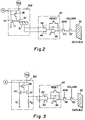
- a unit pixel subassembly 10 forms part of a camera's photosensor array 100 (see array of Fig. 4).
- the unit pixel subassembly 10 is comprised of a photodetector 20, which may be, for example, a CCD device and/or a photodiode.
- the output 22 of the photodetector 20 is connected to a transfer gate 24, a reset gate 26, and a multiplying current mirror 30A.
- the transfer gate 24 allows the charge, accumulated by the photodetector 20 during the exposure period, to be transferred to the multiplying current mirror 30A at the desired time.
- the reset gate 26 allows for the emptying of the photodetector's 20 accumulated charge from the previously completed exposure.
- the reset gate 26 When the reset gate 26 is opened and the camera's shutter 110 (see Fig. 4) is closed the output from the photodetector 20 is integrated for a time equivalent to the previous exposure time so as to cancel dark current and noise. This cancellation occurs within a correlated double sampling circuit 40. The photosensor array 100 is then ready for exposure to a new image.
- the output of the current mirror 30A is a multiple of the current produced by the photodetector 20.
- the current multiplying effect is traditionally accomplished either by connecting the bases or gates of the transistors 32 1 through 32 n in parallel with each other or by making the emitter (or source) areas larger by an integral multiple of the emitter area of an input slide transistor 34.
- Current mirrors of this type operate on the principle that the emitter base voltage (or the gate source voltage) for all the transistors in the current mirror are the same so that each of the collector (drain) currents is the same, and therefore the sum of the currents from the output side T o is a multiple of either the number of transistors in the output side or the ratio of the area.
- the output of the current mirror 30A is switched between two current amplifiers, amplifiers 42 and 44, with gains of +1 and -1, respectively.
- amplifiers 42 and 44 When the photodetector 20 is receiving incident light its amplified current is switched through the +1 gain of amplifier 42 into an integrating amplifier 46 for a given amount of time and then after the shutter is closed the current is integrated through the -1 gain of amplifier 44 for an equal amount of time.
- This operation is known as dual slope, correlated double sampling and it eliminates the effects of dark current and KTC noise. It differs from dual sample CDS in that the signal is switched through two different amplifiers depending on whether the signal represents the image data or the background data wherever dual time CDS uses the same amplification chain. Correlated double sampling also reduces Johnson noise, flicker noise and 1/f noise.
- a similar effect can be achieved by integrating the current from an opaquely masked photodetector through the -1 gain of amplifier 44.
- Using an opaquely masked photodetector adjacent to the active photodetector 20 allows the correlated double sampling technique to be implemented in parallel and decreases readout time.
- the integration of the outputs of the current amplifiers 42 and 44 occurs simultaneously, thus eliminating the need to wait for two integration periods to have output data.
- separate photodetectors are used, small differences in dark current and noise can arise between them.
- the output of the correlated double sampling circuit 40 is selectively connected to a data bus 50 by means of row and column selection transistors 54 and 52, respectively.
- the incorporation of the row and column selection transistors in the pixel unit cell allows for addressing of subsections of the photosensitive array for more rapid image readout in a specific area of interest in the image. This is useful in digital cameras which monitor a scene and are only interested in updating the section of the image associated with moving objects.
- a current mirror circuit 30B that may be substituted for the current mirror 30A provides a second variant of the current mirror function by utilizing an output transistor T o emitter or source whose area is n times the area of the emitter or source of the input transistor T I . This forms a smaller circuit which in turn allocates more area to the photodetector 20.
- Current mirror 30B would be substituted for the current mirror 30A at the connection point marked with a circled A.
- Fig. 3 illustrates a variant of a current mirror labeled 30C that is connectable to the unit pixel subassembly 10 of Fig. 1 at the A labeled point marked with a circle in place of either 30A or 30B.
- the current mirror 30C achieves current multiplication by biasing the emitter base (or gate source) voltage higher on the input side of the current mirror than on the output side. This, more specifically, is accomplished by adjusting the value of R1 and R2. Alternately, a diode junction can be substituted into the emitter or source of the input side of the current mirror 30C in order to provide a fixed voltage bias.
- photosensor array 100 contains unused areas at each photodetector site. It is within these areas that the circuits 30A, B, or C, and circuit 40, along with row and column selection transistors 52 and 54 are located. As previously mentioned the placement of these circuits and transistors in close proximity to their associated photodetector 20 makes a more efficient photosensor array and reduces the need for external support circuitry.
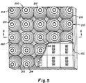
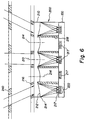
- Fig. 5 illustrates an optic array camera 200 incorporating the photosensor array 100 and a lenslet array 210.
- Fig. 6 illustrates a cross-section of the optic array camera, taken along the section lines 6-6, in Fig. 5.
- the optic array camera 200 is formed with an array 210 of achromatized refractive/diffractive lenslets 212 or refractive lenslets which are centered over photosensitive sites 217.
- the array of lenslets 210 replaces the typical single round lenses that are spaced along one central axis in a camera. To be observed in Fig.
- each lenslet 212 is displaced relative to the fixed sensor-to-sensor distance as a function of its radial distance from the optical axis 213 of the central lenslet which is at the physical center of the array shown.
- the lines 215 appearing around the mechanical optical axis 214 of each lenslet 212 are topographical lines indicating changes in height of the lenslet's surface.
- An opaque mask 216 covers the areas between the lenslets 212 to prevent light from reaching the photodetectors (photosensor) other than by passing through a lenslet.
- the array depicted in Fig. 6 represents only a small portion of an array that is used in an actual camera.
- a typical implementation could consist of 280 x 640 pixels with 3 pixels per lens.
- Other configurations of the lenslets may be used such as forming the outer periphery of each lenslet 212 as a square, hexagon, or circle, without detracting from the invention.
- the optical axis 214 of the lenslets 212 in the lens array 100 are located at a distance which becomes progressively larger than the center-to-center distance of the pixels in the array.
- the displacement of the lenslets optical axis 214 increases radially from the center of the array. Decentering a lens element tends to bend rays from off-axis field angles into the center of the lens groups field of view.
- the optical axis of the lens element By moving the optical axis of the lens element further out radially with increasing distance from the center of the array, the angular location of an object at the center of the field of view for a given lenslet/photodetector pair originates from increasingly off-axis segments of the total field of view.
- the required decenter, for an array element of focal length Fl i necessary to deflect a ray from the desired field angle into the center of the array element's field stop can be determined from the paraxial ray tracing equations.
- the decenter necessary for a given element is approximately a linear function of the element's radial distance from the system's optical axis.
- the lenslet array 210 is positioned over the photosensor array 100 of grouped photosensors 222.
- Each photosensor group 222 is located at an associated photosensitive site 217.
- Each group of photosensors 222 is formed with red (R), green (G), and blue (B) sensors.
- the number of photosensitive sites 217 corresponds in number to at least the number of lenslets 212 in the lenslet array 210.
- the lenslet array 210 is maintained a distance apart from the surfaces of the photosensors by spacers 218 that serve the additional function of being light baffles.
- the opaque masks 216 on the lenslet array 210 combined with a field stop aperture plate 240 limit the field of view of any particular photosensor so that it does not overlap the field of view of its neighbors by a large amount.
- the aperture plate 240 is positioned approximately 0.5mm to 2mm from the surface of the lenslet array 210.
- the aperture plate 240 may be a layer of clear glass having a photoresist mask pattern formed on one of it's surfaces.
- the center of the apertures in the aperture plate 240 are aligned to the center of the field of view of a corresponding lenslet.
- the spacing of the mechanical optical centers 214 increases as a function of each lenslet's radial position radially from the center of the array causing the aperture plate 240 to be slightly larger than the associated lenslet array 210.
- the combination of the opaque areas 216 with the aperture plate 240 and a given lenslet focal length determines the field of view for a photosensitive site 217.
- the lenslet array 210 can be formed of etched quartz, or an epoxy replica on a glass substrate or can be injection molded plastic.
- the lenslets 212 combined with the appropriate field stop aperture plate 240, form images of a small segment of the field of view on each photosensitive site 217.
- the lenslets 212 By forming the lenslets 212 with decentrations of the mechanical optical axis 214 which increase radially across the lenslet array the angle which the axial ray incident on any particular lenslet makes with the surface normal of the plane of the lenslet array 210 will increase as a function of the particular lenslet's radial position on the array. Therefore, by appropriately forming the decenters of each lenslet each photosensitive site 217 will view a different segment of a scene (image). Since each photosensor group 222 has its own lenslet there is no need to reinvert the image with a relay lens.
- any camera system incorporating the present invention, can be extremely compact and flat due to the integration of the above described circuitry which allows for the elimination of support circuit boards which in turn allows for a further decrease in the size of the camera.
- the camera can work in black and white or in color if three unit pixel subassemblies with color filters are formed at each pixel site 217 to pass only assigned frequencies of incident radiation.
- the use of a lenslet that will physically displace incident radiation may be used in lieu of color filters to deflect the appropriate frequency of incident radiation to its assigned photosensor.
- An array of aspheric lenslets can also be used to form images on the photosensor array 100.
- the aforementioned embodiment does not correct for the variation in focal length as a function of wavelength since the lenslet is formed from a single refractive material, therefore the spot size of the incident light varies as a function of color.
- lens F/# Focal Length/Lens Diameter Reducing each lenslet's F/# allows for the reduction of the center-to-center spacing between array elements, since, for a given F/# and detector sensitivity a specific photocurrent is generated.
- an array optic camera is formed with 780 by 640 pixels the length of the long dimension of the array would be 32.5 mm, assuming 3 color pixels (photosensors) at each photosite. This would require a large area of silicon per photosensor array, which would increase part costs and result in lower yields of photosensors from a given wafer size.
- the lenslet diameters can be reduced by 4x to 65 ⁇ m and the length of the array will be reduced to 8.125 mm, resulting in higher photosensor yields and lower part costs.
- the array optic camera can utilize this technique with no decrease in usable photosensitive surface area since the space between photosites is not utilized for light detection, but is rather, empty space.
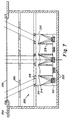
- Fig. 7 illustrates the optic array camera 200 of Fig. 6 positioned in a light tight housing 252 that is exposed to an image via a mechanical shutter 250.
- the mechanical shutter may be any of the typical shutters used in a film type camera.
- the advantage to the optic array camera 200 of Fig. 6 is that no mechanical shutter is required; the photosensors 222 are turned on " or active to capture light from the image focused onto the photosensor array 100. In the Fig. 7 embodiment the photosensors 222 are turned on " generally when camera power is on and image capture occurs when the shutter 250 is activated.
Abstract
The image capture device incorporates an array
of photodetectors (100), utilizing an integral current mirror
formed at each photodetector location to increase
photodetector current output. A correlated double
sampling circuit is also formed at each photodetector
location to sum the current generated by the current
mirror over each exposure period, so as to produce a
voltage proportional to the radiation intensity incident
at each photodetector location. The correlated double
sampling circuit is used to reduce noise in the
photodetected signal and to eliminate the effect of dark
current. Combining the image capture device with a
unique lenslet array (210) forms an extremely compact optical
array camera. An embodiment with a mechanical shutter is
also disclosed.
Description
The present application is related to U.S.
Application Serial Number 08/652,735, filed May 23,
1996, by Mark M. Meyers, and entitled, "A
Diffractive/Refractive Lenslet Array;" U.S.
Application Serial Number 08/417,422, filed April 5,
1995, by Mark M. Meyers, and entitled,  A Blur
Filter For Eliminating Aliasing In Electrically
Sampled Images;" U. S. Application Serial Number
08/663,887, filed June 14, 1996, by Mark M. Meyers,
and entitled,
A Blur
Filter For Eliminating Aliasing In Electrically
Sampled Images;" U. S. Application Serial Number
08/663,887, filed June 14, 1996, by Mark M. Meyers,
and entitled, A Diffractive/Refractive Lenslet
Array Incorporating A Second Aspheric Surface;" U.S.
application Serial Number 08/684,073, filed July 18,
1996, by Mark M. Meyers, and entitled, Lens."
This invention relates generally to the
field of image capture devices and more particularly
to an improvement that integrates circuits into the
areas between the individual photodetectors forming
the image capture device and to their combination
for forming an optic array camera.
U.S. Patent No. 5,471,515, to Fossum, et.
al., entitled Active Pixel Sensor with Intra-Pixel
Charge Transfer." This invention converts the
photogenerated charge stored under the photogate
into a voltage by transferring the charge to a sense
node (typically a capacitor) located within the
active pixel unit cell. Fossum then utilizes dual
sample correlated double sampling of the voltage
based signal to reduce signal noise and eliminate
the effect of dark current from the photosensor.
The voltage associated with the image exposure is
then subtracted from the voltage associated with a
read during a dark sample by a voltage differencing
amplifier located at the end of the row or column of
the photosensors. By using appropriate row and
column selection transistors a subsection of the
array can be read out without the need to read out
the entire image array. The Fossum invention does
not however allow for an increase in the overall
sensitivity of the CCD detector elements, nor does
it envision the utilization of an array optic type
structure to form an image of different segments of
the field of view, although the patent does disclose
the use of a lens array for concentrating light on
the active pixel. Fossum does not include means for
adjusting the overall exposure level of the pixel
internal to the unit cell of the detector array.
Fossum is also performing most of the signal
processing in a voltage amplification mode, whereas
the present invention utilizes the advantages of the
current mode of signal processing.
In U.S. Patent No. 5,004,901, entitled
Current Mirror Amplifier for use in an Optical Data
Medium Driving Apparatus and Servo Circuit" to
Yoshimoto, et. al., photogenerated current from an
optical disk tracking and read sensor is amplified
in fixed steps by a switchable series of current
mirrors, where the current mirrors achieve current
multiplication through the use of output stages that
incorporate either multiple output transistors with
the bases of the output transistors connected in
parallel or by the use of output transistors with
emitter areas that are integral multiples of the
emitter areas of the input side transistor. The
purpose of Yoshimoto's invention is to allow the
utilization of received photocurrents with a large
dynamic range by multiplying the input current by an
adjustable ratio, where the multiple current ratios
are selected through a switchable network of
differential amplifiers. Yoshimoto's invention is
not related to the field of array image sensors and
requires the use of a switchable array of
differencing amplifiers. Yoshimoto's invention does
not integrate the current from the photosensor and
the current is continuously generated by received
light from the laser light emitted by the optical
disk head. Therefore, the sensor is not exposed to
an image with its sensed signals being integrated by
signal processing electronics, as in the current
invention, but is rather used in a continuous
optical disk position monitoring mode. Yoshimoto
does not utilize dual slope correlated double
sampling for noise reduction as disclosed in the
present invention. Yoshimoto does not make any
mention of the use of array optics with a field of
view which varies as a function of radial position
in the sensor array.
The present invention is directed to overcoming
one or more of the problems set forth above. Briefly
summarized, according to one aspect of the present
invention there is provided a photosensitive array
comprised of a plurality of current generating
photodetectors in combination with a plurality of
multiplying current mirrors wherein each multiplying
current mirror is comprised of one input transistor and
two or more output transistors or an output transistor
with an emitter area which is N times the area of the
input transistor. The photocurrent from each
photodetector is multiplied by an integer equal to the
number of output transistors in the multiplying current
mirror.
From the aforementioned it can be seen
that it is a primary object of the present invention
to provide an improved photosensor array
incorporating integrated support electronics.
It is yet another object of the present
invention to provide a short focal length camera
based on the improved photosensor array of the
present invention.
It is another object of the present
invention to provide a compact photosensor array
that incorporates support electronics close to the
source of generated photocurrent.
These and other aspects, objects,
features, and advantages of the present invention
will be more clearly understood and appreciated from
a review of the following detailed description of
the preferred embodiments and appended claims, and
by reference to the accompanying drawings.
The present invention has the advantages of
increased signal current produced by a combination of
current mirrors positioned in close physical proximity to
associated arrayed photodetectors where the increased
signal current represents an increase in sensitivity for
the photosensor array. This increased sensitivity, in
turn, allows for the use of shorter exposure times, or
the use of optics with smaller numerical apertures when
the photosensor array is used in a camera. The use of
lower numerical aperture optics (higher F/#'s) in a
camera allows for greater depth of focus, easier
alignment of optics and photosensor and in general
decreased system costs. In the camera implementation of
the invention either a mechanical or an electrical
shutter may be used.
To facilitate understanding, identical
reference numerals have been used, where possible,
to designate identical elements that are common to
the figures.
Referring to Fig. 1, a unit pixel subassembly 10,
forms part of a camera's photosensor array 100 (see array
of Fig. 4). The unit pixel subassembly 10 is comprised
of a photodetector 20, which may be, for example, a CCD
device and/or a photodiode. The output 22 of the
photodetector 20 is connected to a transfer gate 24, a
reset gate 26, and a multiplying current mirror 30A. The
transfer gate 24 allows the charge, accumulated by the
photodetector 20 during the exposure period, to be
transferred to the multiplying current mirror 30A at the
desired time. When closed the reset gate 26 allows for
the emptying of the photodetector's 20 accumulated charge
from the previously completed exposure. When the reset
gate 26 is opened and the camera's shutter 110 (see Fig.
4) is closed the output from the photodetector 20 is
integrated for a time equivalent to the previous exposure
time so as to cancel dark current and noise. This
cancellation occurs within a correlated double sampling
circuit 40. The photosensor array 100 is then ready for
exposure to a new image.
As is well known the output of the current mirror
30A is a multiple of the current produced by the
photodetector 20. The current multiplying effect is
traditionally accomplished either by connecting the bases
or gates of the transistors 321 through 32n in parallel
with each other or by making the emitter (or source)
areas larger by an integral multiple of the emitter area
of an input slide transistor 34. Current mirrors of this
type operate on the principle that the emitter base
voltage (or the gate source voltage) for all the
transistors in the current mirror are the same so that
each of the collector (drain) currents is the same, and
therefore the sum of the currents from the output side To
is a multiple of either the number of transistors in the
output side or the ratio of the area. This current
multiplication is represented mathematically as follows
as:
Iout = n * Iin
where
- β = transistor current gain (typically between 50 and 200)
In another embodiment of the current mirror 30A a
transistor 36 can be added to the input side Ti of the
current mirror to drive the bases (or gates) of the
output side To of the current mirror and thereby reduce
the effects of leakage current. This is known to reduce
the non-ideality of the above elation to
Iout = n * (Iin / (1+β2 ))
The output of the current mirror 30A is switched
between two current amplifiers, amplifiers 42 and 44,
with gains of +1 and -1, respectively. When the
photodetector 20 is receiving incident light its
amplified current is switched through the +1 gain of
amplifier 42 into an integrating amplifier 46 for a given
amount of time and then after the shutter is closed the
current is integrated through the -1 gain of amplifier 44
for an equal amount of time. This operation is known as
dual slope, correlated double sampling and it eliminates
the effects of dark current and KTC noise. It differs
from dual sample CDS in that the signal is switched
through two different amplifiers depending on whether the
signal represents the image data or the background data
wherever dual time CDS uses the same amplification chain.
Correlated double sampling also reduces Johnson noise,
flicker noise and 1/f noise. A similar effect can be
achieved by integrating the current from an opaquely
masked photodetector through the -1 gain of amplifier 44.
Using an opaquely masked photodetector adjacent to the
active photodetector 20 allows the correlated double
sampling technique to be implemented in parallel and
decreases readout time. The integration of the outputs
of the current amplifiers 42 and 44 occurs
simultaneously, thus eliminating the need to wait for two
integration periods to have output data. However, since
separate photodetectors are used, small differences in
dark current and noise can arise between them.
The output of the correlated double sampling circuit
40 is selectively connected to a data bus 50 by means of
row and column selection transistors 54 and 52,
respectively. The incorporation of the row and column
selection transistors in the pixel unit cell allows for
addressing of subsections of the photosensitive array for
more rapid image readout in a specific area of interest
in the image. This is useful in digital cameras which
monitor a scene and are only interested in updating the
section of the image associated with moving objects.
Referring to Fig. 2, a current mirror circuit 30B
that may be substituted for the current mirror 30A
provides a second variant of the current mirror function
by utilizing an output transistor To emitter or source
whose area is n times the area of the emitter or source
of the input transistor TI. This forms a smaller circuit
which in turn allocates more area to the photodetector
20. Current mirror 30B would be substituted for the
current mirror 30A at the connection point marked with a
circled A.
Fig. 3 illustrates a variant of a current mirror
labeled 30C that is connectable to the unit pixel
subassembly 10 of Fig. 1 at the A labeled point marked
with a circle in place of either 30A or 30B. The current
mirror 30C achieves current multiplication by biasing the
emitter base (or gate source) voltage higher on the input
side of the current mirror than on the output side.
This, more specifically, is accomplished by adjusting the
value of R1 and R2. Alternately, a diode junction can be
substituted into the emitter or source of the input side
of the current mirror 30C in order to provide a fixed
voltage bias.
For a bipolar implementation of the multiplying
current mirror, this technique can be illustrated by the
ebers-moll relation, which is given by
Itr = Is * e (vbe/kt - 1)
where
Vbei = Vbeo + 0.060 v
allows for a current multiplication of approximately 10 x
at 300 k.
A plurality of unit pixel subassemblies 10,
described with respect to Figs. 1-3, find particular
utility in a photosensor array, such as the photosensor
array 100 illustrated in conjunction with a camera 120
and a shutter 110 in Fig. 4 for sensing image radiation.
Unlike conventional photosensor arrays, photosensor array
100 contains unused areas at each photodetector site. It
is within these areas that the circuits 30A, B, or C, and
circuit 40, along with row and column selection
transistors 52 and 54 are located. As previously
mentioned the placement of these circuits and transistors
in close proximity to their associated photodetector 20
makes a more efficient photosensor array and reduces the
need for external support circuitry.
To provide the open space between photodetector
sites without degrading the resolution of the camera a
unique lens array is used. The array is described fully
in U.S. Patent Application Serial Number 08/652,735,
filed on May 23, 1996, by Mark M. Meyers, the inventor of
the present application, and entitled, A
Diffractive/Refractive Lenslet Array." Portions of the
application will be used herein to provide support for
the claims of this invention.
Fig. 5 illustrates an optic array camera
200 incorporating the photosensor array 100 and a
lenslet array 210. Fig. 6 illustrates a cross-section
of the optic array camera, taken along the
section lines 6-6, in Fig. 5. Referring to Figs. 5
and 6 together, the optic array camera 200 is formed
with an array 210 of achromatized
refractive/diffractive lenslets 212 or refractive
lenslets which are centered over photosensitive
sites 217. The array of lenslets 210 replaces the
typical single round lenses that are spaced along
one central axis in a camera. To be observed in
Fig. 5 is that the center of the mechanical optical
axis 214 of each lenslet 212 is displaced relative
to the fixed sensor-to-sensor distance as a function
of its radial distance from the optical axis 213 of
the central lenslet which is at the physical center
of the array shown. The lines 215 appearing around
the mechanical optical axis 214 of each lenslet 212
are topographical lines indicating changes in height
of the lenslet's surface. An opaque mask 216 covers
the areas between the lenslets 212 to prevent light
from reaching the photodetectors (photosensor) other
than by passing through a lenslet. The array
depicted in Fig. 6 represents only a small portion
of an array that is used in an actual camera. A
typical implementation could consist of 280 x 640
pixels with 3 pixels per lens. Other configurations
of the lenslets may be used such as forming the
outer periphery of each lenslet 212 as a square,
hexagon, or circle, without detracting from the
invention.
In order for the array to see different fields
of view the optical axis 214 of the lenslets 212 in the
lens array 100 are located at a distance which becomes
progressively larger than the center-to-center distance
of the pixels in the array. The displacement of the
lenslets optical axis 214 increases radially from the
center of the array. Decentering a lens element tends to
bend rays from off-axis field angles into the center of
the lens groups field of view. By moving the optical
axis of the lens element further out radially with
increasing distance from the center of the array, the
angular location of an object at the center of the field
of view for a given lenslet/photodetector pair originates
from increasingly off-axis segments of the total field of
view.
For instance, the required decenter, for an
array element of focal length Fli, necessary to deflect a
ray from the desired field angle into the center of the
array element's field stop can be determined from the
paraxial ray tracing equations. The paraxial equations
are
y' = yo + nu(t/n) n'u' = no uo - y
where
Therefore, the displacement for a given
lenslet with power ( = 1/FLi ) that is necessary to
bend the central ray from a given angle of incidence uo to
a desired angle u', after refraction is given by
d = y = (no uo - n'u')/
The invention utilizes an array of lenslets
where the local displacement of the lens group's optical
axis varies as a function of radial position relative to
the center of the system's image optical axis, so that,
to first order
d(r) = ( no uo (r) - n'u'(r) )/
The invention consists of adjusting the lenslet
decenters so that u'(r) = 0 for the central ray within a
given lenslet's field of view. In this case the decenter
necessary for a given element is approximately a linear
function of the element's radial distance from the
system's optical axis.
Referring again to Fig. 6, the lenslet
array 210 is positioned over the photosensor array
100 of grouped photosensors 222. Each photosensor
group 222 is located at an associated photosensitive
site 217. Each group of photosensors 222 is formed
with red (R), green (G), and blue (B) sensors. The
number of photosensitive sites 217 corresponds in
number to at least the number of lenslets 212 in the
lenslet array 210. The lenslet array 210 is
maintained a distance apart from the surfaces of the
photosensors by spacers 218 that serve the
additional function of being light baffles. The
opaque masks 216 on the lenslet array 210, combined
with a field stop aperture plate 240 limit the field
of view of any particular photosensor so that it
does not overlap the field of view of its neighbors
by a large amount. The aperture plate 240 is
positioned approximately 0.5mm to 2mm from the
surface of the lenslet array 210. The aperture
plate 240 may be a layer of clear glass having a
photoresist mask pattern formed on one of it's
surfaces.
The center of the apertures in the
aperture plate 240 are aligned to the center of the
field of view of a corresponding lenslet. The
spacing of the mechanical optical centers 214
increases as a function of each lenslet's radial
position radially from the center of the array
causing the aperture plate 240 to be slightly larger
than the associated lenslet array 210. The
combination of the opaque areas 216 with the
aperture plate 240 and a given lenslet focal length
determines the field of view for a photosensitive
site 217. The lenslet array 210 can be formed of
etched quartz, or an epoxy replica on a glass
substrate or can be injection molded plastic.
The lenslets 212, combined with the
appropriate field stop aperture plate 240, form
images of a small segment of the field of view on
each photosensitive site 217. By forming the
lenslets 212 with decentrations of the mechanical
optical axis 214 which increase radially across the
lenslet array the angle which the axial ray incident
on any particular lenslet makes with the surface
normal of the plane of the lenslet array 210 will
increase as a function of the particular lenslet's
radial position on the array. Therefore, by
appropriately forming the decenters of each lenslet
each photosensitive site 217 will view a different
segment of a scene (image). Since each photosensor
group 222 has its own lenslet there is no need to
reinvert the image with a relay lens.
Therefore, any camera system, incorporating the
present invention, can be extremely compact and flat
due to the integration of the above described
circuitry which allows for the elimination of
support circuit boards which in turn allows for a
further decrease in the size of the camera. The
camera can work in black and white or in color if
three unit pixel subassemblies with color filters
are formed at each pixel site 217 to pass only
assigned frequencies of incident radiation. The use
of a lenslet that will physically displace incident
radiation may be used in lieu of color filters to
deflect the appropriate frequency of incident
radiation to its assigned photosensor.
An array of aspheric lenslets can also be
used to form images on the photosensor array 100.
However, the aforementioned embodiment does not
correct for the variation in focal length as a
function of wavelength since the lenslet is formed
from a single refractive material, therefore the
spot size of the incident light varies as a function
of color.
By utilizing a multiplying current mirror to
increase the photocurrent generated at each photosite the
effective sensitivity of the photosensor array is
increased. Prior art photosensitive arrays (such as CCD
arrays) require the use of lenses with very high
numerical apertures (low F/#'s, typically on the order of
F/1.8 to F/4.0) which are more difficult to align, harder
to keep in focus and in general cost more than lower F/#
objective lenses. For an array optic camera with a field
of view which varies as a function of radial position in
the photosensitive array, the use of a photosensor unit
cell with increased sensitivity will allow for the use of
lower F/# optics. The definition of lens F/# is
F/# = Focal Length/Lens Diameter
Reducing each lenslet's F/# allows for the reduction of
the center-to-center spacing between array elements,
since, for a given F/# and detector sensitivity a
specific photocurrent is generated. The illumination
incident on the detector array from a given lenslet is
proportional to the (F/#)2. Therefore, if the sensitivity
is increased by x, the F/# can be reduced by x1/2. For
instance, if an array optic camera, without multiplying
current mirror, is used with a lenslet having a F/# = 4.0
and a FL = 0.5 mm the lenslet's diameter would be 250 µm.
Therefore, if an array optic camera is formed with 780 by
640 pixels the length of the long dimension of the array
would be 32.5 mm, assuming 3 color pixels (photosensors)
at each photosite. This would require a large area of
silicon per photosensor array, which would increase part
costs and result in lower yields of photosensors from a
given wafer size. By incorporating a current mirror with
a multiplication factor of 16 at each photosite the
lenslet diameters can be reduced by 4x to 65 µm and the
length of the array will be reduced to 8.125 mm,
resulting in higher photosensor yields and lower part
costs. The array optic camera can utilize this technique
with no decrease in usable photosensitive surface area
since the space between photosites is not utilized for
light detection, but is rather, empty space.
Fig. 7 illustrates the optic array camera 200
of Fig. 6 positioned in a light tight housing 252 that is
exposed to an image via a mechanical shutter 250. The
mechanical shutter may be any of the typical shutters
used in a film type camera. The advantage to the optic
array camera 200 of Fig. 6 is that no mechanical shutter
is required; the photosensors 222 are turned on" or
active to capture light from the image focused onto the
photosensor array 100. In the Fig. 7 embodiment the
photosensors 222 are turned on" generally when camera
power is on and image capture occurs when the shutter 250
is activated.
The invention has been described with
reference to a preferred embodiment; However, it
will be appreciated that variations and
modifications can be effected by a person of
ordinary skill in the art without departing from the
scope of the invention.
- 10
- unit pixel subassembly
- 20
- photodetector
- 22
- output
- 24
- transfer gate
- 26
- reset gate
- 30A
- multiplying current mirror
- 30B
- current mirror circuit
- 30C
- current mirror
- 321 - 32n
- output side transistors
- 34
- input side transistors
- 36
- transistor
- 40
- correlated double sampling circuit
- 42
- +1 amp
- 44
- -1 amp
- 46
- integrating amplifier
- 50
- data bus
- 52
- column selection transistors
- 54
- row selection transistors
- 100
- photosensor array
- 110
- shutter
- 120
- camera
- 200
- optic array camera
- 210
- lenslet array
- 212
- achromatized refractive/diffractive lenslet
- 213
- optical axis (central)
- 214
- optical axis (central)
- 215
- lines
- 216
- opaque mask
- 217
- photosensitive sites
- 218
- light spacers and/or baffles
- 222
- photosensors
- 240
- field stop aperture plate
- 250
- mechanical shutter
- 252
- light tight housing
- To
- output transistor
- TI
- input transistor
Claims (10)
- A compact image capture device comprising:an array of spaced apart radiation sensors for providing output signals that are a function of the incident radiation from an image onto each radiation sensor;array electronics dispersed in the spaces between the spaced apart radiation sensors for receiving the provided output signals so as amplify the provided output signals to facilitate image capture; anda lens array positioned so as to focus the radiation of an image to be captured onto said radiation sensors.
- A compact image capture device according to Claim 1 and further comprising:a mechanical shutter positioned proximate said lens array for controlling which images are radiated onto said array of radiation sensors.
- A compact image capture device according to Claim 1 wherein said array electronics is comprised in part of a plurality of current multipliers, corresponding in number to the number of radiation sensors, each connected to an associated radiation sensor.
- An image capturing device comprising:an array of spaced apart groups of radiation sensors for providing output signals that are a function of the frequencies of incident radiation from an image onto each radiation sensor;array electronics dispersed in the spaces between the spaced apart groups of radiation sensors for receiving and amplifying their provided output signals to facilitate image capture; anda lens array positioned so as to focus the frequencies of radiation from an image to be captured onto associated ones of the radiation sensors in each of the groups of said radiation sensors such that each radiation sensor in a group provides an output signal that is a function of its sensed frequency.
- A photosensor array of current generating photodetectors each in combination with an associated multiplying current mirror located adjacent thereto and comprised of one input transistor and at least two output transistors where the generated photocurrent from each photodetector is multiplied by an integer equal to the number of output transistors in the associated multiplying current mirror and to provide the multiplied current as an output signal.
- The photosensor array according to Claim 5 and further comprising:correlated double sampling circuits connected to receive the output signal of an associated multiplying current mirror for providing an output that minimizes the dark current and noise from the current generating photodetectors.
- The photosensor array according to Claim 6 and further comprising:row and column select means for connecting the output from the correlated double sampling circuits to a data bus.
- The photosensor array according to Claim 6 in combination with a camera wherein said photosensor array is exposed to the image to be captured by said camera so as to provide multiplied correlated double sampled current signals that represent said image to the data bus.
- The photosensor array according to Claim 5 and further comprising, a lenslet array having a number of lenslets corresponding in number to the number of current generating photodetectors each lenslet positioned so as to focus incident radiation onto an associated current generating photodetector, each lenslet being a refractive/diffractive lenslet wherein the center of the mechanical optical axis of each lenslet is displaced relative to the displacement of its associated photosensor's radial distance from the optical axis of the lenslet located in the center of the array.
- A photosensor array of current generating photodetectors each in combination with an associated multiplying current mirror located adjacent thereto and comprised of one input transistor and at least one output transistor having an emitter area which is equal to an integer multiple of the input transistor emitter area where the generated photocurrent from each photodetector is multiplied by an integer equal to the ratio of the output divided by the input transistor emitter area so as to provide an integer multiplied current as an output signal.
Applications Claiming Priority (2)
| Application Number | Priority Date | Filing Date | Title |
|---|---|---|---|
| US08/699,306 US6141048A (en) | 1996-08-19 | 1996-08-19 | Compact image capture device |
| US699306 | 1996-08-19 |
Publications (1)
| Publication Number | Publication Date |
|---|---|
| EP0825764A2 true EP0825764A2 (en) | 1998-02-25 |
Family
ID=24808758
Family Applications (1)
| Application Number | Title | Priority Date | Filing Date |
|---|---|---|---|
| EP97202459A Withdrawn EP0825764A2 (en) | 1996-08-19 | 1997-08-08 | Compact image capture device |
Country Status (3)
| Country | Link |
|---|---|
| US (1) | US6141048A (en) |
| EP (1) | EP0825764A2 (en) |
| JP (1) | JPH1090789A (en) |
Cited By (3)
| Publication number | Priority date | Publication date | Assignee | Title |
|---|---|---|---|---|
| EP0833502A2 (en) * | 1996-09-26 | 1998-04-01 | Eastman Kodak Company | Compact image capture device with local image storage |
| EP0840502A2 (en) * | 1996-11-04 | 1998-05-06 | Eastman Kodak Company | Compact digital camera with segmented fields of view |
| WO2005069607A1 (en) * | 2004-01-20 | 2005-07-28 | Frauhofer-Gesellschaft Zur Förderung Der Angewandten Forschung E.V. | Image recording system, and use thereof |
Families Citing this family (81)
| Publication number | Priority date | Publication date | Assignee | Title |
|---|---|---|---|---|
| US6515701B2 (en) * | 1997-07-24 | 2003-02-04 | Polaroid Corporation | Focal plane exposure control system for CMOS area image sensors |
| NO305728B1 (en) * | 1997-11-14 | 1999-07-12 | Reidar E Tangen | Optoelectronic camera and method of image formatting in the same |
| JP3657780B2 (en) | 1998-06-30 | 2005-06-08 | 株式会社東芝 | Imaging device |
| US6572017B1 (en) * | 1999-08-12 | 2003-06-03 | Telxon Corporation | Optical device employing a mirror array for increasing the apparent resolution of a photosensor |
| US6750437B2 (en) * | 2000-08-28 | 2004-06-15 | Canon Kabushiki Kaisha | Image pickup apparatus that suitably adjusts a focus |
| JP2003060990A (en) * | 2001-08-10 | 2003-02-28 | Victor Co Of Japan Ltd | Solid-state imaging device and read method thereof |
| JP3518529B2 (en) * | 2001-08-17 | 2004-04-12 | ソニー株式会社 | Solid-state imaging device |
| US8064650B2 (en) * | 2002-07-10 | 2011-11-22 | Hewlett-Packard Development Company, L.P. | File management of digital images using the names of people identified in the images |
| US7423679B2 (en) * | 2002-12-20 | 2008-09-09 | Eastman Kodak Company | Imaging system having extended useful latitude |
| US6801719B1 (en) * | 2003-03-14 | 2004-10-05 | Eastman Kodak Company | Camera using beam splitter with micro-lens image amplification |
| US7310477B2 (en) * | 2003-08-26 | 2007-12-18 | Eastman Kodak Company | Photographic film cartridge or cassette systems with microlens |
| JP2005167665A (en) * | 2003-12-03 | 2005-06-23 | Sanyo Electric Co Ltd | Image signal processor, image signal processing method, image signal processing program, controller and controlling method for solid-state imaging element |
| US7375701B2 (en) * | 2004-07-01 | 2008-05-20 | Carestream Health, Inc. | Scanless virtual retinal display system |
| US20060044451A1 (en) * | 2004-08-30 | 2006-03-02 | Eastman Kodak Company | Wide angle lenslet camera |
| JP4306603B2 (en) * | 2004-12-20 | 2009-08-05 | ソニー株式会社 | Solid-state imaging device and driving method of solid-state imaging device |
| US7375312B2 (en) * | 2005-01-26 | 2008-05-20 | Avago Technologies Ecbu Ip Pte Ltd | Planar fly's eye detector |
| IL167637A (en) * | 2005-03-24 | 2009-09-22 | Semi Conductor Devices An Elbi | Method and system for determining the rate of non uniformity of bolometer based systems |
| IL167641A (en) * | 2005-03-24 | 2011-07-31 | Semi Conductor Devices An Elbit Systems Rafael Partnership | System for measuring and compensating for the case temperature variations in a bolometer based system |
| US7511323B2 (en) * | 2005-08-11 | 2009-03-31 | Aptina Imaging Corporation | Pixel cells in a honeycomb arrangement |
| FR2918449B1 (en) * | 2007-07-02 | 2010-05-21 | Ulis | DEVICE FOR DETECTING INFRARED RADIATION WITH BOLOMETRIC DETECTORS |
| US8902321B2 (en) | 2008-05-20 | 2014-12-02 | Pelican Imaging Corporation | Capturing and processing of images using monolithic camera array with heterogeneous imagers |
| US11792538B2 (en) | 2008-05-20 | 2023-10-17 | Adeia Imaging Llc | Capturing and processing of images including occlusions focused on an image sensor by a lens stack array |
| US8866920B2 (en) | 2008-05-20 | 2014-10-21 | Pelican Imaging Corporation | Capturing and processing of images using monolithic camera array with heterogeneous imagers |
| EP2502115A4 (en) | 2009-11-20 | 2013-11-06 | Pelican Imaging Corp | Capturing and processing of images using monolithic camera array with heterogeneous imagers |
| JPWO2011068185A1 (en) * | 2009-12-04 | 2013-04-18 | 株式会社ニコン | Imaging optical system and microscope apparatus |
| KR101824672B1 (en) | 2010-05-12 | 2018-02-05 | 포토네이션 케이맨 리미티드 | Architectures for imager arrays and array cameras |
| US8878950B2 (en) | 2010-12-14 | 2014-11-04 | Pelican Imaging Corporation | Systems and methods for synthesizing high resolution images using super-resolution processes |
| GB2488519A (en) | 2011-02-16 | 2012-09-05 | St Microelectronics Res & Dev | Multi-channel image sensor incorporating lenslet array and overlapping fields of view. |
| JP2014519741A (en) | 2011-05-11 | 2014-08-14 | ペリカン イメージング コーポレイション | System and method for transmitting and receiving array camera image data |
| US20130265459A1 (en) | 2011-06-28 | 2013-10-10 | Pelican Imaging Corporation | Optical arrangements for use with an array camera |
| EP2726930A4 (en) | 2011-06-28 | 2015-03-04 | Pelican Imaging Corp | Optical arrangements for use with an array camera |
| US9229096B2 (en) * | 2011-07-27 | 2016-01-05 | Semiconductor Components Industries, Llc | Time-of-flight imaging systems |
| WO2013043761A1 (en) | 2011-09-19 | 2013-03-28 | Pelican Imaging Corporation | Determining depth from multiple views of a scene that include aliasing using hypothesized fusion |
| EP2761534B1 (en) | 2011-09-28 | 2020-11-18 | FotoNation Limited | Systems for encoding light field image files |
| US9412206B2 (en) | 2012-02-21 | 2016-08-09 | Pelican Imaging Corporation | Systems and methods for the manipulation of captured light field image data |
| US9210392B2 (en) | 2012-05-01 | 2015-12-08 | Pelican Imaging Coporation | Camera modules patterned with pi filter groups |
| WO2014005123A1 (en) | 2012-06-28 | 2014-01-03 | Pelican Imaging Corporation | Systems and methods for detecting defective camera arrays, optic arrays, and sensors |
| US20140002674A1 (en) | 2012-06-30 | 2014-01-02 | Pelican Imaging Corporation | Systems and Methods for Manufacturing Camera Modules Using Active Alignment of Lens Stack Arrays and Sensors |
| CN107346061B (en) | 2012-08-21 | 2020-04-24 | 快图有限公司 | System and method for parallax detection and correction in images captured using an array camera |
| WO2014032020A2 (en) | 2012-08-23 | 2014-02-27 | Pelican Imaging Corporation | Feature based high resolution motion estimation from low resolution images captured using an array source |
| US9214013B2 (en) | 2012-09-14 | 2015-12-15 | Pelican Imaging Corporation | Systems and methods for correcting user identified artifacts in light field images |
| CN104685860A (en) | 2012-09-28 | 2015-06-03 | 派力肯影像公司 | Generating images from light fields utilizing virtual viewpoints |
| US9143711B2 (en) | 2012-11-13 | 2015-09-22 | Pelican Imaging Corporation | Systems and methods for array camera focal plane control |
| WO2014097507A1 (en) * | 2012-12-21 | 2014-06-26 | パナソニック株式会社 | Solid-state image pickup element |
| US9462164B2 (en) | 2013-02-21 | 2016-10-04 | Pelican Imaging Corporation | Systems and methods for generating compressed light field representation data using captured light fields, array geometry, and parallax information |
| US9253380B2 (en) | 2013-02-24 | 2016-02-02 | Pelican Imaging Corporation | Thin form factor computational array cameras and modular array cameras |
| US9638883B1 (en) | 2013-03-04 | 2017-05-02 | Fotonation Cayman Limited | Passive alignment of array camera modules constructed from lens stack arrays and sensors based upon alignment information obtained during manufacture of array camera modules using an active alignment process |
| US9774789B2 (en) | 2013-03-08 | 2017-09-26 | Fotonation Cayman Limited | Systems and methods for high dynamic range imaging using array cameras |
| US8866912B2 (en) | 2013-03-10 | 2014-10-21 | Pelican Imaging Corporation | System and methods for calibration of an array camera using a single captured image |
| US9521416B1 (en) | 2013-03-11 | 2016-12-13 | Kip Peli P1 Lp | Systems and methods for image data compression |
| US9888194B2 (en) | 2013-03-13 | 2018-02-06 | Fotonation Cayman Limited | Array camera architecture implementing quantum film image sensors |
| WO2014165244A1 (en) | 2013-03-13 | 2014-10-09 | Pelican Imaging Corporation | Systems and methods for synthesizing images from image data captured by an array camera using restricted depth of field depth maps in which depth estimation precision varies |
| WO2014164550A2 (en) | 2013-03-13 | 2014-10-09 | Pelican Imaging Corporation | System and methods for calibration of an array camera |
| US9106784B2 (en) | 2013-03-13 | 2015-08-11 | Pelican Imaging Corporation | Systems and methods for controlling aliasing in images captured by an array camera for use in super-resolution processing |
| WO2014153098A1 (en) | 2013-03-14 | 2014-09-25 | Pelican Imaging Corporation | Photmetric normalization in array cameras |
| US9578259B2 (en) | 2013-03-14 | 2017-02-21 | Fotonation Cayman Limited | Systems and methods for reducing motion blur in images or video in ultra low light with array cameras |
| US9497429B2 (en) | 2013-03-15 | 2016-11-15 | Pelican Imaging Corporation | Extended color processing on pelican array cameras |
| US9633442B2 (en) | 2013-03-15 | 2017-04-25 | Fotonation Cayman Limited | Array cameras including an array camera module augmented with a separate camera |
| US9497370B2 (en) | 2013-03-15 | 2016-11-15 | Pelican Imaging Corporation | Array camera architecture implementing quantum dot color filters |
| WO2014145856A1 (en) | 2013-03-15 | 2014-09-18 | Pelican Imaging Corporation | Systems and methods for stereo imaging with camera arrays |
| US10122993B2 (en) | 2013-03-15 | 2018-11-06 | Fotonation Limited | Autofocus system for a conventional camera that uses depth information from an array camera |
| US9445003B1 (en) | 2013-03-15 | 2016-09-13 | Pelican Imaging Corporation | Systems and methods for synthesizing high resolution images using image deconvolution based on motion and depth information |
| WO2015048694A2 (en) | 2013-09-27 | 2015-04-02 | Pelican Imaging Corporation | Systems and methods for depth-assisted perspective distortion correction |
| WO2015070105A1 (en) | 2013-11-07 | 2015-05-14 | Pelican Imaging Corporation | Methods of manufacturing array camera modules incorporating independently aligned lens stacks |
| US10119808B2 (en) | 2013-11-18 | 2018-11-06 | Fotonation Limited | Systems and methods for estimating depth from projected texture using camera arrays |
| EP3075140B1 (en) | 2013-11-26 | 2018-06-13 | FotoNation Cayman Limited | Array camera configurations incorporating multiple constituent array cameras |
| US10089740B2 (en) | 2014-03-07 | 2018-10-02 | Fotonation Limited | System and methods for depth regularization and semiautomatic interactive matting using RGB-D images |
| US9247117B2 (en) | 2014-04-07 | 2016-01-26 | Pelican Imaging Corporation | Systems and methods for correcting for warpage of a sensor array in an array camera module by introducing warpage into a focal plane of a lens stack array |
| US9521319B2 (en) | 2014-06-18 | 2016-12-13 | Pelican Imaging Corporation | Array cameras and array camera modules including spectral filters disposed outside of a constituent image sensor |
| CN113256730B (en) | 2014-09-29 | 2023-09-05 | 快图有限公司 | System and method for dynamic calibration of an array camera |
| US9942474B2 (en) | 2015-04-17 | 2018-04-10 | Fotonation Cayman Limited | Systems and methods for performing high speed video capture and depth estimation using array cameras |
| US10482618B2 (en) | 2017-08-21 | 2019-11-19 | Fotonation Limited | Systems and methods for hybrid depth regularization |
| MX2022003020A (en) | 2019-09-17 | 2022-06-14 | Boston Polarimetrics Inc | Systems and methods for surface modeling using polarization cues. |
| EP4042366A4 (en) | 2019-10-07 | 2023-11-15 | Boston Polarimetrics, Inc. | Systems and methods for augmentation of sensor systems and imaging systems with polarization |
| KR20230116068A (en) | 2019-11-30 | 2023-08-03 | 보스턴 폴라리메트릭스, 인크. | System and method for segmenting transparent objects using polarization signals |
| CN115552486A (en) | 2020-01-29 | 2022-12-30 | 因思创新有限责任公司 | System and method for characterizing an object pose detection and measurement system |
| KR20220133973A (en) | 2020-01-30 | 2022-10-05 | 인트린식 이노베이션 엘엘씨 | Systems and methods for synthesizing data to train statistical models for different imaging modalities, including polarized images |
| WO2021243088A1 (en) | 2020-05-27 | 2021-12-02 | Boston Polarimetrics, Inc. | Multi-aperture polarization optical systems using beam splitters |
| US11954886B2 (en) | 2021-04-15 | 2024-04-09 | Intrinsic Innovation Llc | Systems and methods for six-degree of freedom pose estimation of deformable objects |
| US11290658B1 (en) | 2021-04-15 | 2022-03-29 | Boston Polarimetrics, Inc. | Systems and methods for camera exposure control |
| US11689813B2 (en) | 2021-07-01 | 2023-06-27 | Intrinsic Innovation Llc | Systems and methods for high dynamic range imaging using crossed polarizers |
Family Cites Families (41)
| Publication number | Priority date | Publication date | Assignee | Title |
|---|---|---|---|---|
| US3910683A (en) * | 1970-07-28 | 1975-10-07 | Minolta Camera Kk | Optical low-pass filter |
| US4085411A (en) * | 1976-04-16 | 1978-04-18 | Sprague Electric Company | Light detector system with photo diode and current-mirror amplifier |
| JPS54154728A (en) * | 1978-05-25 | 1979-12-06 | Boehringer Mannheim Gmbh | Manufacture of alphaa*44*44chlorobenzoylaminoo ethyl**phenoxyyisoethylacetic acid |
| DE2823164A1 (en) * | 1978-05-26 | 1979-11-29 | Bayer Ag | METHOD FOR MANUFACTURING HEXAHYDROPHTHALIC ANHYDRIDE |
| US4318123A (en) * | 1980-06-05 | 1982-03-02 | Rca Corporation | Solid-state, color-encoding television camera |
| US4323925A (en) * | 1980-07-07 | 1982-04-06 | Avco Everett Research Laboratory, Inc. | Method and apparatus for arraying image sensor modules |
| JPS5789731A (en) * | 1980-11-25 | 1982-06-04 | Canon Inc | Focusing screen |
| JPS57184376A (en) * | 1981-05-09 | 1982-11-13 | Sony Corp | Signal output circuit of image pickup device |
| US4377753A (en) * | 1981-06-01 | 1983-03-22 | Eastman Kodak Company | High resolution optical-addressing device and electronic scanner and/or printer apparatus employing such device |
| JPS59193699A (en) * | 1983-04-18 | 1984-11-02 | Niles Parts Co Ltd | Plane driving type speaker |
| US4573177A (en) * | 1984-02-06 | 1986-02-25 | The United States Of America As Represented By The Secretary Of The Air Force | Bi-directional current differencer for complementary charge coupled device (CCD) outputs |
| NL8400805A (en) * | 1984-03-14 | 1985-10-01 | Philips Nv | CHARGE COUPLED TRANSVERSAL FILTER. |
| US4708436A (en) * | 1985-07-12 | 1987-11-24 | Rca Corporation | Optical imager with diffractive lenticular array |
| US4689291A (en) * | 1985-08-30 | 1987-08-25 | Xerox Corporation | Pedestal-type microlens fabrication process |
| JPS62144459A (en) * | 1985-12-19 | 1987-06-27 | Ricoh Co Ltd | Complete contact type sensor |
| US5004901A (en) * | 1987-06-04 | 1991-04-02 | Mitsubishi Denki Kabushiki Kaisha | Current mirror amplifier for use in an optical data medium driving apparatus and servo-circuit |
| JPS63100879A (en) * | 1986-10-17 | 1988-05-02 | Hitachi Ltd | Solid-state image pickup device |
| US4973833A (en) * | 1988-09-28 | 1990-11-27 | Minolta Camera Kabushiki Kaisha | Image sensor including logarithmic converters |
| US5187358A (en) * | 1989-02-15 | 1993-02-16 | Canon Kabushiki Kaisha | Image reading device having a telecentric optical system and a blazed diffraction grating |
| US4994664A (en) * | 1989-03-27 | 1991-02-19 | Massachusetts Institute Of Technology | Optically coupled focal plane arrays using lenslets and multiplexers |
| US5151790A (en) * | 1990-07-23 | 1992-09-29 | Fuji Photo Film Co., Ltd. | Image pickup device for stabilizing optical aberrations |
| US5076687A (en) * | 1990-08-28 | 1991-12-31 | Massachusetts Institute Of Technology | Optical ranging apparatus |
| US5233174A (en) * | 1992-03-11 | 1993-08-03 | Hughes Danbury Optical Systems, Inc. | Wavefront sensor having a lenslet array as a null corrector |
| US5497269A (en) * | 1992-06-25 | 1996-03-05 | Lockheed Missiles And Space Company, Inc. | Dispersive microlens |
| US5329312A (en) * | 1992-08-17 | 1994-07-12 | Eastman Kodak Company | DC level control circuitry for CCD images |
| JP2987016B2 (en) * | 1992-08-28 | 1999-12-06 | 松下電器産業株式会社 | Phase grating optical low-pass filter |
| US5340978A (en) * | 1992-09-30 | 1994-08-23 | Lsi Logic Corporation | Image-sensing display panels with LCD display panel and photosensitive element array |
| US5760834A (en) * | 1992-09-30 | 1998-06-02 | Lsi Logic | Electronic camera with binary lens element array |
| US5529936A (en) * | 1992-09-30 | 1996-06-25 | Lsi Logic Corporation | Method of etching a lens for a semiconductor solid state image sensor |
| JP3438205B2 (en) * | 1993-02-25 | 2003-08-18 | 株式会社リコー | Digital electronic camera device |
| US5841126A (en) * | 1994-01-28 | 1998-11-24 | California Institute Of Technology | CMOS active pixel sensor type imaging system on a chip |
| US5471515A (en) * | 1994-01-28 | 1995-11-28 | California Institute Of Technology | Active pixel sensor with intra-pixel charge transfer |
| US5461425A (en) * | 1994-02-15 | 1995-10-24 | Stanford University | CMOS image sensor with pixel level A/D conversion |
| JPH08107194A (en) * | 1994-10-03 | 1996-04-23 | Fuji Photo Optical Co Ltd | Solid state image sensor |
| US5705807A (en) * | 1994-10-24 | 1998-01-06 | Nissan Motor Co., Ltd. | Photo detecting apparatus for detecting reflected light from an object and excluding an external light componet from the reflected light |
| US5814803A (en) * | 1994-12-23 | 1998-09-29 | Spectra-Physics Scanning Systems, Inc. | Image reader with multi-focus lens |
| US5708263A (en) * | 1995-12-27 | 1998-01-13 | International Business Machines Corporation | Photodetector array |
| US5784178A (en) * | 1996-03-06 | 1998-07-21 | Dyna Image Corporation | High performance contact image sensor |
| US5844238A (en) * | 1996-03-27 | 1998-12-01 | David Sarnoff Research Center, Inc. | Infrared imager using room temperature capacitance sensor |
| US5754056A (en) * | 1996-04-23 | 1998-05-19 | David Sarnoff Research Center, Inc. | Charge detector with long integration time |
| US5838176A (en) * | 1996-07-11 | 1998-11-17 | Foveonics, Inc. | Correlated double sampling circuit |
-
1996
- 1996-08-19 US US08/699,306 patent/US6141048A/en not_active Expired - Fee Related
-
1997
- 1997-08-08 EP EP97202459A patent/EP0825764A2/en not_active Withdrawn
- 1997-08-18 JP JP9221744A patent/JPH1090789A/en not_active Withdrawn
Cited By (6)
| Publication number | Priority date | Publication date | Assignee | Title |
|---|---|---|---|---|
| EP0833502A2 (en) * | 1996-09-26 | 1998-04-01 | Eastman Kodak Company | Compact image capture device with local image storage |
| EP0833502A3 (en) * | 1996-09-26 | 2000-01-05 | Eastman Kodak Company | Compact image capture device with local image storage |
| EP0840502A2 (en) * | 1996-11-04 | 1998-05-06 | Eastman Kodak Company | Compact digital camera with segmented fields of view |
| EP0840502A3 (en) * | 1996-11-04 | 2000-01-05 | Eastman Kodak Company | Compact digital camera with segmented fields of view |
| US6137535A (en) * | 1996-11-04 | 2000-10-24 | Eastman Kodak Company | Compact digital camera with segmented fields of view |
| WO2005069607A1 (en) * | 2004-01-20 | 2005-07-28 | Frauhofer-Gesellschaft Zur Förderung Der Angewandten Forschung E.V. | Image recording system, and use thereof |
Also Published As
| Publication number | Publication date |
|---|---|
| US6141048A (en) | 2000-10-31 |
| JPH1090789A (en) | 1998-04-10 |
Similar Documents
| Publication | Publication Date | Title |
|---|---|---|
| US6141048A (en) | Compact image capture device | |
| US6137535A (en) | Compact digital camera with segmented fields of view | |
| EP1031239B1 (en) | Optoelectronic camera and method for image formatting in the same | |
| EP0893915A2 (en) | Compact image sensor with display integrally attached | |
| US6750437B2 (en) | Image pickup apparatus that suitably adjusts a focus | |
| EP1062802B1 (en) | Active linear sensor | |
| EP1302986B1 (en) | Photodetector with high dynamic range and increased operating temperature | |
| JP2003318381A (en) | Solid-state imaging device and camera | |
| KR20110128130A (en) | Solid-state imaging device and electronic equipment | |
| JP2001518759A (en) | Sensor device | |
| JP2004309701A (en) | Range-finding/photometric sensor and camera | |
| EP0833502A2 (en) | Compact image capture device with local image storage | |
| WO2020079960A1 (en) | Imaging device and solid-state imaging device | |
| EP2061235B1 (en) | Sensitivity correction method and imaging device | |
| CN100498496C (en) | Photometry/ranging solid state image pick-up device and image pick-up apparatus using such device | |
| CN110352489B (en) | Autofocus system for CMOS imaging sensor | |
| JPH0637289A (en) | Solid-state image sensing device | |
| Monteiro et al. | Fast Hartmann-Shack wavefront sensors manufactured in standard CMOS technology | |
| JP2001346104A (en) | Solid-state image pickup device and image pickup device using it | |
| WO2011055117A1 (en) | Detector | |
| JP2004191630A (en) | Imaging apparatus | |
| JP4500849B2 (en) | Solid-state imaging device for AEAF | |
| JPH11337815A (en) | Solid photographing device and range finder for camera | |
| JP3120787B2 (en) | Device and method for monitoring spectral characteristics and sensitivity | |
| JP2006344904A (en) | Solid-state imaging device and temperature detector of solid-state image sensor |
Legal Events
| Date | Code | Title | Description |
|---|---|---|---|
| PUAI | Public reference made under article 153(3) epc to a published international application that has entered the european phase |
Free format text: ORIGINAL CODE: 0009012 |
|
| AK | Designated contracting states |
Kind code of ref document: A2 Designated state(s): AT BE CH DE DK ES FI FR GB GR IE IT LI LU MC NL PT SE |
|
| STAA | Information on the status of an ep patent application or granted ep patent |
Free format text: STATUS: THE APPLICATION HAS BEEN WITHDRAWN |
|
| 18W | Application withdrawn |
Withdrawal date: 19990505 |