EP0821448A2 - PC card assembly and method of assembling the same - Google Patents

PC card assembly and method of assembling the same Download PDF

Info

Publication number
EP0821448A2
EP0821448A2 EP97112579A EP97112579A EP0821448A2 EP 0821448 A2 EP0821448 A2 EP 0821448A2 EP 97112579 A EP97112579 A EP 97112579A EP 97112579 A EP97112579 A EP 97112579A EP 0821448 A2 EP0821448 A2 EP 0821448A2
Authority
EP
European Patent Office
Prior art keywords
circuit board
card connector
solder tails
printed circuit
soldering
Prior art date
Legal status (The legal status is an assumption and is not a legal conclusion. Google has not performed a legal analysis and makes no representation as to the accuracy of the status listed.)
Withdrawn
Application number
EP97112579A
Other languages
German (de)
French (fr)
Other versions
EP0821448A3 (en
Inventor
Hideyuki Hirata
Toshihisa Hirata
Current Assignee (The listed assignees may be inaccurate. Google has not performed a legal analysis and makes no representation or warranty as to the accuracy of the list.)
Molex LLC
Original Assignee
Molex LLC
Priority date (The priority date is an assumption and is not a legal conclusion. Google has not performed a legal analysis and makes no representation as to the accuracy of the date listed.)
Filing date
Publication date
Application filed by Molex LLC filed Critical Molex LLC
Publication of EP0821448A2 publication Critical patent/EP0821448A2/en
Publication of EP0821448A3 publication Critical patent/EP0821448A3/en
Withdrawn legal-status Critical Current

Links

Images

Classifications

    • HELECTRICITY
    • H01ELECTRIC ELEMENTS
    • H01RELECTRICALLY-CONDUCTIVE CONNECTIONS; STRUCTURAL ASSOCIATIONS OF A PLURALITY OF MUTUALLY-INSULATED ELECTRICAL CONNECTING ELEMENTS; COUPLING DEVICES; CURRENT COLLECTORS
    • H01R43/00Apparatus or processes specially adapted for manufacturing, assembling, maintaining, or repairing of line connectors or current collectors or for joining electric conductors
    • H01R43/20Apparatus or processes specially adapted for manufacturing, assembling, maintaining, or repairing of line connectors or current collectors or for joining electric conductors for assembling or disassembling contact members with insulating base, case or sleeve
    • H01R43/205Apparatus or processes specially adapted for manufacturing, assembling, maintaining, or repairing of line connectors or current collectors or for joining electric conductors for assembling or disassembling contact members with insulating base, case or sleeve with a panel or printed circuit board
    • HELECTRICITY
    • H01ELECTRIC ELEMENTS
    • H01RELECTRICALLY-CONDUCTIVE CONNECTIONS; STRUCTURAL ASSOCIATIONS OF A PLURALITY OF MUTUALLY-INSULATED ELECTRICAL CONNECTING ELEMENTS; COUPLING DEVICES; CURRENT COLLECTORS
    • H01R12/00Structural associations of a plurality of mutually-insulated electrical connecting elements, specially adapted for printed circuits, e.g. printed circuit boards [PCB], flat or ribbon cables, or like generally planar structures, e.g. terminal strips, terminal blocks; Coupling devices specially adapted for printed circuits, flat or ribbon cables, or like generally planar structures; Terminals specially adapted for contact with, or insertion into, printed circuits, flat or ribbon cables, or like generally planar structures
    • H01R12/70Coupling devices
    • H01R12/71Coupling devices for rigid printing circuits or like structures
    • H01R12/712Coupling devices for rigid printing circuits or like structures co-operating with the surface of the printed circuit or with a coupling device exclusively provided on the surface of the printed circuit
    • H01R12/716Coupling device provided on the PCB

Landscapes

  • Engineering & Computer Science (AREA)
  • Manufacturing & Machinery (AREA)
  • Coupling Device And Connection With Printed Circuit (AREA)
  • Details Of Connecting Devices For Male And Female Coupling (AREA)
  • Manufacturing Of Electrical Connectors (AREA)
  • Multi-Conductor Connections (AREA)

Abstract

Disclosed is an improved PC card assembly (1) and a method of assembling a PC card connector assembly comprising the steps of: placing a first PC card connector (3) to a first side (2a) of a printed circuit board (2); soldering the surface mount solder tails (11) of the signal terminals (8) of the first connector to a signal circuit pattern (12) formed on the surface of the first side of the circuit board; soldering the through-hole solder tails (13) of the ground terminals (9) of the first PC card connector within through-holes (14) made in the circuit board; placing a second PC card connector (4) to an opposite side (2b) of the circuit board; soldering the surface mount solder tails (20) of the signal terminals (17) of the second connector to a circuit pattern (21) formed on the surface of the opposite side of the circuit board; mounting a separate ground terminal piece (18) to the second PC card connector; and soldering the solder tails (22) of the ground terminal piece (18) to a ground circuit pattern (23) on the opposite side of the printed circuit board. Visual inspection of the solder tails with respect to the circuit board can be performed subsequent to each step.

Description

Field of the Invention
The present invention relates to a PC card connector assembly and a method of assembling a PC card connector assembly comprising a printed circuit board and a PC card connector on each side of the printed circuit board, each PC card connector having signal terminals and ground terminals.
Description of the Prior Art
The signal terminals and ground terminals of known PC card connectors typically have solder tails formed in a right angle configuration and positioned at the rear end of the PC card connector such that the ends of the solder tails are directed to and in contact with circuit traces on the underlying printed circuit board. These solder tails are often fixed to the circuit board by dip-soldering whereby they are inserted in through-holes made in the circuit board and then soldered.
In applications where two PC card connectors are used in a stacked or "dual port" configuration, the circuit board uses a relatively large area allotted to the layout of the through-holes for accommodating each row of solder tails (often two rows of tails for the signal terminals and one for the ground terminals) for each connector. One attempt to solve the problem of occupying such a large area with through-holes is to place one PC card connector on one side of the circuit board and a second PC card connector on the other side of the circuit board. In assembling such an arrangement, however, there are some tradeoffs due to the layout that must be considered. Specifically, since the solder tails of the signal and ground terminals are arranged in at least two different rows, alignment of the solder tails with respect to the circuit pattern formed on the circuit board is difficult to inspect and correct. Particularly, visually inspecting and correcting the alignment of the solder tails positioned toward the inside of the assembly is more difficult than inspecting and correcting the solder tails positioned toward the outside of the assembly.
Summary of the Invention
One object of the present invention is to provide a dual port PC connector assembly occupying a relatively small area on the printed circuit board, while allowing and facilitating visual inspection and correction of the alignment of the solder tails of the signal and ground terminals.
To attain this and other objects, a PC card connector assembly is improved according to the present invention in that it comprises: a first PC card connector for mounting to a printed circuit board including signal terminals having surface mount solder tails adapted to be surface mounted to a first side of the circuit board; a first ground piece mounted on the first PC card connector and including through-hole solder tails adapted to be mounted within holes in the circuit board; a second PC card connector for mounting to the circuit board including signal terminals having surface mount solder tails adapted to be surface mounted to an opposite side of the circuit board; and a second ground piece for mounting on the second PC card connector and including surface mount solder tails adapted to be mounted to the surface of the opposite side of the circuit board.
Further according to the invention, a method of forming a PC card connector assembly is disclosed, the PC card connector assembly including a printed circuit board and first and second PC card connectors fixed to opposite sides of the circuit board, each PC card connector having signal terminals and ground terminals, the method of forming the assembly comprising the steps of: attaching the first PC card connector to one side of the printed circuit board, the solder tails of the signal terminals of the first PC card connector being of surface mount type, and the solder tails of the ground piece of the first PC card connector being of dip-soldering type; soldering the solder tails of the signal terminals of the first PC card connector to the signal circuit pattern formed on the surface of the one side of the circuit board; soldering the solder tails of the ground piece of the first PC card connector within the through-holes of a ground circuit of the printed circuit board; attaching the second PC card connector to an opposite side of the circuit board, the solder tails of the signal terminals of the second PC card connector being of surface mount type; soldering the solder tails of the signal terminals of the second PC card connector to the signal circuit pattern formed on the surface of the other side of the circuit board; assembling a ground terminal piece onto the second PC card connector, the solder tails of the ground terminal piece being of surface mount type; and soldering the solder tails of the ground terminal piece of the second PC card connector to a ground circuit pattern formed on the surface of the opposite side of the circuit board.
Soldering the solder tails of the signal terminals and soldering the solder tails of the ground piece of the first PC card connector on the first side of the circuit board can be effected simultaneously by reflow soldering, for example.
The surface mount solder tails of the signal and ground terminals of the second PC card connector are soldered to the circuit pattern formed on the opposite side of the circuit board, thus reducing the total area occupied on the circuit board by the dual port PC card assembly. In additional, visual inspection of the solder tails of the signal terminals of the first PC connector can be performed without obstruction by the solder tails of the ground terminals. The solder tails of the ground terminals can also be inspected from the opposite side without obstruction. Visual inspection of the solder tails of the signal terminals of the second PC connector can be performed without obstruction by the solder tails of the ground terminals, which are soldered subsequent to the signal terminals. The solder tails of the ground terminals can also be inspected easily, i.e., without visual obstruction, after it is assembled on the second PC card connector.
Other objects and advantages of the present invention will be understood from the following description of a preferred embodiment of the present invention, which is illustrated in the accompanying drawings:
  • FIGURE 1 is an enlarged longitudinal section view of a PC card connector assembly, which is made according to the present invention;
  • FIGURE 2 is a plan view of the PC card connector assembly;
  • FIGURE 3 is a rear view of the PC card connector assembly; and
  • FIGURE 4 is a perspective view of a ground terminal piece to be assembled to the second PC connector fixed to the opposite side of the printed circuit board.
  • Detailed Description of the Preferred Embodiment
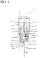
    Referring to the drawings and first to Figures 1 through 3, a PC card connector assembly 1 comprises a printed circuit board 2 and first and second PC card connectors 3 and 4 fixed to front and rear sides 2a and 2b of printed circuit board 2, respectively. Printed circuit board 2 has a receptacle connector 5 for connecting the printed circuit board to a group of wires or other electrical boards via an associated plug connector (not shown).
    PC card connector 3 mounted on the front side of the printed circuit board includes right angle-configured signal terminals 8 which have two rows of contacts 7 located in a card slot 6 of a connector housing 10 of PC card connector 3. Surface mount solder tails 11 of signal terminals 8 are adapted to be surface mounted to a conductive pattern 12 of a signal circuit (not shown) formed on the surface of front side 2a of printed circuit board 2. The connector housing 10 has a ground terminal piece 9 mounted thereto. Right angle-configured solder tails 13 of ground piece 9 are adapted to be dip-soldered within through-holes 14 of a ground circuit (not shown) on front side 2a of circuit board 2.
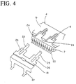
    PC card connector 4 mounted on rear side 2b of printed circuit board 2 includes right angle-configured signal terminals 17 which have two rows of contacts 16 located in a card slot 15 of a connector housing 19. Surface mount solder tails 20 of signal terminals 17 are adapted to be surface-mounted to a conductive pattern 21 of a signal circuit formed on the surface of rear side 2b of circuit board 2. Connector housing 19 has a ground terminal piece 18 mounted thereon. Ground piece 18 comprises a lateral base, mount projections 26 integrally connected to one side of the lateral base, each projection having a contact 25 integrally connected thereto, and right angle-configured solder tails 22 integrally connected to the other side of the lateral base. Connector housing 19 has insertion slots with notched edges 24 in opposite sides of the slots, thus permitting the insertion of mount projections 26 of ground piece 18 into connector housing 19. Surface mount solder tails 22 of ground terminal piece 18 are adapted to be surface mounted to a conductive pattern 23 of a ground circuit (not shown) also formed on the surface of rear side 2b of circuit board 2.
    Now, the method of assembling the PC card connector assembly will be described. The method comprises the steps of: placing the first PC card connector 3 on a first side 2a of the printed circuit board 2, inserting the through-hole solder tails 13 of ground piece 9 in the through-holes 14 of the circuit board, and placing the surface mount solder tails 11 of the signal terminals 8 on the conductive pattern 12 formed on the surface of first side 2a of the circuit board. The soldering of both sets of solder tails can be effected simultaneously, for example by reflow soldering. Prior to soldering, the location and alignment of the surface mount solder tails 11 relative to the conductive pattern 12 is visually inspected so that misalignments and other problems with the solder tails can be detected and corrected before soldering. No visual obstructions interfere with the inspection of the solder tails 11 since they are located on the outside of the assembly, thereby facilitating visual inspection thereof. Also, visual inspection of the through-hole solder tails 13 of ground piece 9 can be performed from the opposite side 2b of circuit board 2, i.e. looking for the presence of a tail within or protruding from the through-hole itself, since no connector has been placed over the tails to obstruct the inspection.
    After fixing the first PC connector 3 to the first side 2a of circuit board 2, a second PC connector 4 is placed on the second or opposite side 2b of the circuit board, and the required solder connections are made. The second PC connector 4 is designed to permit the subsequent assembly of separate ground piece 18 to the connector housing 19.
    After placing the second PC connector 4 on the second side of the circuit board (prior to assembling the separate ground piece), the alignment of surface mount solder tails 20 of signal terminals 17 relative to a conductive pattern 21 formed on the surface of the second side of the circuit board is visually inspected, and misalignments and other problems with the signal terminal solder tails 20 can be detected and corrected. The inspection and correction of misalignments of the solder tails can be performed without difficulty because there are no obstacles that interfere. After checking the signal terminal solder tail alignment, the solder tails are soldered to the conductive pattern 21, for example by reflow soldering. After soldering, visual inspection of the solder joint can also be made.
    After assembling the second connector to the second side of the circuit board, the ground piece 18 is press-fit into the connector housing 19 of the second PC card connector so that solder tails 22 of the ground piece are in contact with the corresponding portions of a conductive pattern 23 of a ground circuit formed on the second side of the circuit board. Visual inspection of the relative positioning between solder tails 22 and the corresponding portions of conductive pattern 23 of the ground circuit can be made easily because the interface is visually free of any obstacles.
    After visual inspection is performed on the positioning of the tails, the tails are soldered to the ground circuit. After soldering, the solder joints can be inspected as well.
    The PC card connector assembly according to the present invention results.
    It is understood that the invention may be embodied in other specific forms without departing from the spirit or central characteristics thereof. The present examples and embodiments, therefore, are to be considered in all respects as illustrative and not restrictive, and the invention is not to be limited to the details given herein.

    Claims (5)

    1. A PC card connector assembly (1) for mounting to a printed circuit board (2) and for receiving two parallel pc cards, comprising:
      a first pc card connector (3) for mounting to a first side (2a) of the circuit board and including signal terminals (8) having surface mount solder tails (11) adapted to be surface mounted to a surface of the first side of the circuit board;
      a first ground piece (9) mounted on the first pc card connector having through-hole solder tails (13) adapted to be mounted within through-holes (14) in the circuit board;
      a second pc card connector (4) for mounting to a second side of the circuit board (2a) and including signal terminals (17) having surface mount solder tails (20) adapted to be surface mounted to a surface of the second side of the circuit board; and
      a second ground piece (18) mounted on the second pc card connector (4) having surface mount solder tails adapted to be mounted to the surface of the second side of the circuit board.
    2. A PC card connector assembly (1) as set forth in claim 1 wherein the second ground piece (18) includes a lateral base with projections (26) integrally formed therewith which are received in slots (24) in the connector housing.
    3. A PC card connector assembly (1) as set forth in claim 1 further comprising a receptacle connector (5) adapted to be mounted on the printed circuit board so that the PC card connector assembly (1) may be connected to a mating electrical apparatus by way of the receptacle connector.
    4. A method of assembling a PC card connector assembly (1) including a printed circuit board (2) and first and second PC card connectors (3,4) fixed to opposite sides (2a, 2b) of the printed circuit board, the first PC card connector (3) including signal terminals (8) having surface mount type solder tails (11) and a first ground piece (9) having through-hole type solder tails (13), the second PC card connector (4) including signal terminals (17) having surface mount type solder tails (20) and a separate second ground piece (18) having surface mount type solder tails, the method comprising the steps of:
      placing the first PC card connector (3) on the first side (2a) of the printed circuit board;
      soldering the solder tails (11) of the signal terminals (8) of the first PC card connector to a signal circuit pattern (12) formed on a surface of the first side of the printed circuit board;
      soldering the solder tails (13) of the first ground piece (9) within the through-holes (14) of a ground circuit of the printed circuit board;
      placing the second PC card connector (4) on the second side (2b) of the printed circuit board;
      soldering the solder tails (20) of the signal terminals (17) of the second PC card connector to a signal circuit pattern (21) formed on a surface of the second side (2b) of the printed circuit board;
      mounting the second ground piece (18) onto the second PC card connector (4); and
      soldering the solder tails (22) of the second ground piece (18) to a ground circuit pattern (23) formed on the surface of the second side of the circuit board.
    5. A method of forming a PC card connector assembly (1) according to claim 3 wherein soldering of the solder tails (11) of the signal terminals (8), and soldering of the solder tails (13) of the ground piece (9) of the first PC card connector (3) on the one side (2a) of the printed circuit board (2) are effected simultaneously.
    EP97112579A 1996-07-26 1997-07-23 PC card assembly and method of assembling the same Withdrawn EP0821448A3 (en)

    Applications Claiming Priority (2)

    Application Number Priority Date Filing Date Title
    JP8215531A JP3066570B2 (en) 1996-07-26 1996-07-26 Method of manufacturing connector assembly for PC card
    JP215531/96 1996-07-26

    Publications (2)

    Publication Number Publication Date
    EP0821448A2 true EP0821448A2 (en) 1998-01-28
    EP0821448A3 EP0821448A3 (en) 1999-03-03

    Family

    ID=16673978

    Family Applications (1)

    Application Number Title Priority Date Filing Date
    EP97112579A Withdrawn EP0821448A3 (en) 1996-07-26 1997-07-23 PC card assembly and method of assembling the same

    Country Status (6)

    Country Link
    US (1) US5964597A (en)
    EP (1) EP0821448A3 (en)
    JP (1) JP3066570B2 (en)
    MY (1) MY122003A (en)
    SG (1) SG67407A1 (en)
    TW (1) TW460101U (en)

    Families Citing this family (11)

    * Cited by examiner, † Cited by third party
    Publication number Priority date Publication date Assignee Title
    MY123239A (en) 1998-12-18 2006-05-31 Molex Inc Card-receiving connector with grounding terminal
    TW415706U (en) * 1999-05-15 2000-12-11 Hon Hai Prec Ind Co Ltd Electronic card connector device
    US6978335B2 (en) * 2000-06-30 2005-12-20 02Micro International Limited Smart card virtual hub
    US6459602B1 (en) 2000-10-26 2002-10-01 O2 Micro International Limited DC-to-DC converter with improved transient response
    US7000249B2 (en) * 2001-05-18 2006-02-14 02Micro Pre-boot authentication system
    US7797729B2 (en) * 2000-10-26 2010-09-14 O2Micro International Ltd. Pre-boot authentication system
    US20030013414A1 (en) * 2001-07-13 2003-01-16 Huang Yishao Max Radio system for providing wireless connectivity between digital devices
    US6913196B2 (en) * 2002-02-20 2005-07-05 O2Micro International Limited Dual mode controller for ISO7816 and USB enabled smart cards
    TWM243815U (en) * 2003-10-14 2004-09-11 Molex Taiwan Ltd Electronic card connector
    TW200824192A (en) * 2006-11-24 2008-06-01 Fci Connectors Singapore Pte Electric connector
    FR2971095B1 (en) * 2011-02-01 2013-11-08 Tyco Electronics France Sas ELECTRICAL CONNECTOR FOR A SECURITY RETENTION SYSTEM HAVING A GROUND TERMINAL

    Citations (3)

    * Cited by examiner, † Cited by third party
    Publication number Priority date Publication date Assignee Title
    DE3909263A1 (en) * 1988-03-22 1989-10-05 Teradyne Inc ELECTRICAL CONNECTING DEVICE
    DE29601655U1 (en) * 1996-01-31 1996-03-28 Siemens Ag Module circuit board with connector
    US5516294A (en) * 1992-12-30 1996-05-14 Berg Technology, Inc. Coaxial interconnection system

    Family Cites Families (8)

    * Cited by examiner, † Cited by third party
    Publication number Priority date Publication date Assignee Title
    US5299089A (en) * 1991-10-28 1994-03-29 E. I. Dupont De Nemours & Co. Connector device having two storage decks and three contact arrays for one hard disk drive package or two memory cards
    US5308251A (en) * 1992-08-10 1994-05-03 The Whitaker Corporation Mounting bracket with ESD protection for an electrical connector
    US5305182A (en) * 1992-10-14 1994-04-19 Chen Teng Ka Read/write unit for two integrated circuit cards
    JP2567629Y2 (en) * 1993-03-23 1998-04-02 バーグ・テクノロジー・インコーポレーテッド Connector device
    US5316488A (en) * 1993-06-04 1994-05-31 Molex Incorporated Connector apparatus for IC packs
    US5399105A (en) * 1994-04-29 1995-03-21 The Whitaker Corporation Conductive shroud for electrical connectors
    US5478260A (en) * 1994-07-29 1995-12-26 The Whitaker Corporation Grounding for electrical connectors
    US5470259A (en) * 1994-12-05 1995-11-28 The Whitaker Corporation Grounding shroud for surface mounted electrical connector

    Patent Citations (3)

    * Cited by examiner, † Cited by third party
    Publication number Priority date Publication date Assignee Title
    DE3909263A1 (en) * 1988-03-22 1989-10-05 Teradyne Inc ELECTRICAL CONNECTING DEVICE
    US5516294A (en) * 1992-12-30 1996-05-14 Berg Technology, Inc. Coaxial interconnection system
    DE29601655U1 (en) * 1996-01-31 1996-03-28 Siemens Ag Module circuit board with connector

    Non-Patent Citations (1)

    * Cited by examiner, † Cited by third party
    Title
    CZESCHKA, ADELBERG: "Steckverbinder f}r Oberfl{chenmontage" FEINWERKTECHNIK & MESSTECHNIK,1987, XP002088144 W.Germany *

    Also Published As

    Publication number Publication date
    US5964597A (en) 1999-10-12
    EP0821448A3 (en) 1999-03-03
    TW460101U (en) 2001-10-11
    MY122003A (en) 2006-03-31
    JPH1040982A (en) 1998-02-13
    SG67407A1 (en) 1999-09-21
    JP3066570B2 (en) 2000-07-17

    Similar Documents

    Publication Publication Date Title
    KR100344866B1 (en) Surface Mount Electrical Connectors
    US5688130A (en) Electrical connector assembly for pc cards
    US6315620B1 (en) System, method, and device for a pre-loaded straddle mounted connector assembly
    US6527588B2 (en) Electrical connector with integrated PCB assembly
    US6863572B1 (en) Electrical connector with shock support
    EP0561202A1 (en) Integral ground terminal and tail shield
    KR100297956B1 (en) Improved connector assembly having signal and ground terminals
    US6176743B1 (en) Electrical adapter
    US5964597A (en) PC card assembly and method of assembling the same
    EP0661779A1 (en) Multi-connector assembly
    US5709555A (en) High density card edge connection system with outrigger and sequentially connected contacts
    US6638111B1 (en) Board mounted electrical connector with improved ground terminals
    US6135784A (en) LIF PGA socket
    US6095824A (en) Electrical connector assembly
    US6322392B1 (en) Ground plate structure for a PC card connector assembly
    EP0245161A1 (en) Fixing structure for contact pins of electrical connector
    US5997312A (en) Grounding contact for high speed, high density connector
    US6685504B1 (en) Shielded electrical connector assembly having reliable grounding capabilities
    EP0499436B1 (en) Fish hook hold-downs
    EP0643448B1 (en) Coaxial connector for connection to a printed circuit board
    US20120178299A1 (en) Surface-mount on-board diagnostics connector-pin assembly
    US6736647B1 (en) Printed circuit board connector
    US6685505B1 (en) Electrical connector assembly having ground member
    US20100221930A1 (en) Plug device, plug connector, and method for producing the plug connector
    US6949989B2 (en) Electronic signal filter including solderless ground clip having surge protection and shielding features

    Legal Events

    Date Code Title Description
    PUAI Public reference made under article 153(3) epc to a published international application that has entered the european phase

    Free format text: ORIGINAL CODE: 0009012

    AK Designated contracting states

    Kind code of ref document: A2

    Designated state(s): AT BE CH DE DK ES FI FR GB GR IE IT LI LU MC NL PT SE

    PUAL Search report despatched

    Free format text: ORIGINAL CODE: 0009013

    AK Designated contracting states

    Kind code of ref document: A3

    Designated state(s): AT BE CH DE DK ES FI FR GB GR IE IT LI LU MC NL PT SE

    AKX Designation fees paid
    STAA Information on the status of an ep patent application or granted ep patent

    Free format text: STATUS: THE APPLICATION IS DEEMED TO BE WITHDRAWN

    18D Application deemed to be withdrawn

    Effective date: 19990904

    REG Reference to a national code

    Ref country code: DE

    Ref legal event code: 8566