FIELD OF THE INVENTION
The present invention relates to noncontact charging
device, and a charger and a cordless equipment used in a
noncontact charging device as well as to a noncontact charging
device, and more particularly to a charging device for charging
in a noncontact form and by making use of mutual induction a
secondary battery incorporated in a cordless equipment such
as a cordless handset or a portable telephone set, and to a
charger and a cordless equipment used in a noncontact charging
device.
BACKGROUND OF THE INVENTION
There has been proposed to execute power transmission
to a cordless equipment by making use of mutual induction
(electromagnetic induction) by an induction coil for the
purpose of charging a secondary battery such as a nickel-cadmium
battery or a lithium ion battery incorporated in the
cordless equipment such as a cordless handset or a portable
telephone set, and the scheme as described above is disclosed,
for instance, in Japanese Patent Laid-Open Publication No. SHO
54-12422, Japanese Patent Laid-Open Publication No. HEI 5-64375,
Japanese Patent Laid-Open Publication No. HEI 5-300662,
and Japanese Patent Laid-Open Publication No. HEI 7-170312.
In a noncontact charging device for executing power
transmission by making use of mutual induction, a primary side
induction coil is provided in a charger, a secondary side
induction coil is provided in a cordless equipment, an LC
resonance circuit is formed in the charger as well as in the
cordless equipment with a combination with a capacitor, and
power is transmitted to the cordless equipment from the charger
by making use of electromagnetic induction under high
frequency oscillation.
In order to efficiently transmit power by making use of
mutual induction, it is necessary to set a degree of magnetic
connection between a primary side induction coil and a
secondary side induction to an appropriate value under high
frequency resonance, and in order to set the degree of
electromagnetic connection to an appropriate degree, it is
required to satisfy the prerequisites not only that the
cordless equipment must be positioned against the charger when
charged, but also that a mounting position for the coil in each
of the charger and cordless equipment has been set with high
precision.
In other words, when charging, the primary side induction
coil and the secondary side induction coil must be magnetically
connected at a prespecified gap to each other so that they are
connected to each other with a high magnetic flux density
atmosphere, and also it is desired that the magnetic connection
area is large, and otherwise waste of electric power
disadvantageously increases.
However, a primary side induction coil and a secondary
side induction coil in a conventional type of noncontact
charging device are wound coils, and for this reason it is
difficult to set mounting positions for the induction coils
in a charger as well as in a cordless equipment with high
precision, and also the construction for mounting is
complicated. In a case of a wound coil, if the wound coil is
one having a specific form with a core, precision in the
mounting position for an induction coil is high, but in this
case construction of the induction coil is complicated and the
cost is high.
Also the magnetic connection area is enlarged when a
winding diameter or the number of turns of winding increases,
but this makes size and weight of the induction coil larger,
and it is hard to use this type of induction coil in a cordless
equipment with portability such as a portable telephone set
which is desired to be less in size and weight.
Also in a noncontact charging device based on the mutual
induction system as described above, even in a state where a
cordless equipment has not been set in a charger (in a stand-by
state), if a metallic conductor such as coin is placed on a
charger while the primary side induction coil in the charger
is oscillating at the same output level as that in charging,
an eddy current flows in the metallic conductor due to a
magnetic field caused by the primary side induction coil, which
generates induction heating and increase in wasteful power
consumption.
SUMMARY OF THE INVENTION
It is a main object of the present invention to provide
& noncontact charging device with little wasteful power
consumption, and more particularly to provide a noncontact
charging device as well as a charger and a cordless equipment
each with little wasteful power consumption in which mutual
induction can efficiently be executed with an appropriate gap
by using low cost and high productivity induction coils without
making construction of the coil itself or mounting
construction thereof complicated and further a marge magnetic
connection area can be obtained without making size and weight
of the induction coil larger, and further to provide a
noncontact charger and a cordless equipment with little
wasteful power consumption by improving the devices so that
substantial induction heating will not be generated even it
a metallic conductor is placed by mistake on the charger in
the stand-by state.
In order to achieve the objects as described above, in
the noncontact charging device according to the invention for
transmitting power, by making use of mutual induction between
a primary side induction coil provided in a charger and a
secondary side induction coil provided in a cordless equipment
incorporating a secondary battery therein, from the charger
to the cordless and charging the secondary battery, capacitors
are connected in parallel to the primary side induction coil
as well as to the secondary side induction coil respectively
and an LC parallel resonance circuit is formed with this
parallel connection in each of the charger and the cordless
equipment, each of the primary side induction coil and the
secondary side induction coil is built with a sheet coil and
the sheet coils are provided and fixed in the charger and the
cordless equipment so that the sheet coils face to each other
at a specified gap from each other in the charging state where
the cordless equipment is set in the charger.
In the noncontact charging device according to the
present invention, a double tuning circuit is formed with a
combination of LC parallel resonance circuits each formed in
a charger and a cordless equipment respectively, and power
transmission from the charger to the cordless equipment is
executed by means of mutual induction by the double tuning
circuit. Each of the primary side induction coil and secondary
side induction coil is formed with a sheet coil, so that
construction of the coil itself and mounting construction
thereof are not complicated, and with this feature, mutual
induction between the induction coils can efficiently be
executed with an appropriate gap and also with a large magnetic
connection area without making size of weight of the coils
larger.
With the invention, in the noncontact charging device,
the gap is set to a dimension where a critical connection state
can be achieved between the primary side induction coil and
the secondary side induction coil.
As a critical connection state is achieved depending on
a magnetic connection coefficient in a double tuning circuit
based on a combination of LC parallel resonance circuits, in
the invention, the critical connection state is achieved when
a gap between the primary side induction coil and secondary
side induction coil is set to an appropriate value, and then
efficient power transmission is executed with maximum and
single peak frequency characteristics.
With the invention, in the noncontact charging device
according to the present invention, the sheet coil is spirally
patterned on a plane.
In the noncontact charging device according to the above
invention, a sheet coil is spirally patterned on one plane,
so that a large plane-formed magnetic field can be obtained
with a small space, which insures a large magnetic connection
area without making size and weight of coils larger.
With the invention, in the noncontact charging device
according to the present invention, the sheet coil comprises
a pattern inductor patterned on a printed board.
In the noncontact charging device according to the
present invention, the sheet coil comprises a pattern inductor
patterned on a printed board, and the pattern inductors can
be mass-produced with stable performance and high productivity
and also with low cost, so that the sheet coil can comprise
a high quality and low cost product.
The invention provides a charger in the noncontact
charging device according to the present invention.
The charger according to the present invention functions
as a charger in the noncontact charging device according to
the present invention.
The invention provides a cordless equipment in the
noncontact charging device according to the present invention.
The cordless equipment according to the above invention
functions as a cordless invention in the noncontact charging
device according to the present invention.
Also to achieve the objects as described above, with the
invention, the noncontact charger according to the invention
for transmitting power to a cordless equipment including a
secondary side induction coil and a secondary battery by making
use of mutual induction by a primary side coil to charge the
secondary battery comprises a resonance circuit including a
primary side induction coil; a resonance state switching means
for switching a resonant voltage level in the resonance circuit
between a high level and a low level; and a mutual induction
state detecting means for checking whether the primary side
induction coil is in the mutual induction state or not according
to oscillation amplitude in the resonance circuit, and in the
noncontact charger, the a oscillation voltage level in the
resonance circuit is act to a high level by the resonance state
switching means when a mutual induction state is being
detected by the mutual induction state detecting means, and
otherwise is set to a low level by the resonance state
switching means.
In the noncontact charger according to the above
invention, when a cordless equipment is set in the charger,
the primary side induction coil is set in the mutual induction
state, and in this state, a mutual induction state detecting
means detects the mutual induction state, and an oscillation
voltage level in the resonance circuit is set by the resonance
state switching means to a high level. In contrast, in a state
where a cordless equipment has not been set in the charger,
the primary side induction coil is set in a state other than
the mutual induction state, and in this state, the mutual
induction state detecting means detects that the primary side
induction coil is not in the mutual induction state, and a
oscillation voltage level in the resonance circuit is set by
the resonance state switching means to a low level.
With the invention, in the noncontact charger according
to the present invention, the mutual induction state detecting
means comprises a variable amplifier for catching change in
oscillation amplitude in the resonance circuit as a voltage
change and amplifying it, and a comparator for comparing an
output voltage from the variable amplifier to a reference value
for comparison, and the comparator outputs a determination
signal indicating according to a result of comparison whether
the primary side induction coil is in the mutual induction state
or not, and the variable amplifier sets an offset voltage in
the state where the mutual induction state has not been effected
to a level lower than that in the state where the mutual
induction state has been effected according to the
determination signal.
In the noncontact charger according to the above
invention, the variable amplifier catches change in
oscillation amplitude in the resonance circuit as voltage
change and amplifies it, the comparator compares an output
voltage from the variable amplifier to a reference value for
comparison, and an determination signal indicating whether the
primary side induction coil is in the mutual induction state
or not is outputted according to a result of comparison. This
determination signal is given to the variable amplifier, and
an offset voltage in the variable amplifier when it is indicated
by the determination signal that the primary side induction
coil is not in the mutual induction state is set to a lever
lower than that in the state where the primary side induction
coil is in the mutual induction state, so that the offset
voltage is switched according to whether a resonance voltage
in the resonance circuit is at a high level or at a low level.
With this feature, even if there is only one reference voltage
for comparison of the comparator, or regardless of whether a
resonance voltage in the resonance circuit is at a high level
or at a low level, whether the primary side induction coil is
in the mutual induction state or not can accurately be
determined.
With the invention, in the noncontact charger according
to the present inventon, the variable amplifier sets an
amplification factor in the state where it is determined
according to a determination signal outputted from the
comparator that the mutual induction state has not been
effected to a level higher than that in the state where the
mutual induction state has been effected.
In the noncontact charger according to the above
invention, a determination signal is given to the variable
amplifier, and an amplification factor for the variable
amplifier in a state other than the mutual induction state is
set to a value larger than that in the mutual induction state,
so that, in the state where an output voltage from the variable
amplifier has largely changed in response to change in
oscillation amplitude and a oscillation voltage level in the
resonance circuit is at a low level at the state other than
the mutual induction state, and also in the stand-by (idle)
state where a cordless equipment is not set in the charger,
even if the oscillation amplitude changes a little when a
cordless equipment is set in the charger, the fact that the
cordless equipment has been set is accurately detected by the
comparator.
With the invention, the noncontact charger according to
the present invention comprises a delay circuit for delaying
a timing when the determination signal is given to the
oscillation state switching means.
In the noncontact charger according to the above
invention, input of a determination signal into the
oscillation state switching means is delayed by the delay
circuit. With this feature, switching of oscillation state
is executed after output state of the variable amplifier is
stabilized.
With the invention, in the noncontact charger according
to the present invention, the mutual induction state detecting
means comprises a first comparator for comparing a resonance
voltage obtained according to oscillation amplitude in the
resonance circuit to a first reference value for comparison
and a second comparator for comparing a resonance voltage
obtained according to oscillation amplitude in the resonance
circuit to a second reference value for comparison larger than
the first reference value for comparison, and a determination
signal indicating whether the primary side induction coil is
in the mutual induction state or not is outputted with a
combination of an output signal from the first comparator and
that from the second comparator.
In the noncontact charger according to the above
invention, the first comparator compares a resonance voltage
obtained according to oscillation amplitude in the resonance
circuit to a first reference value for comparison; the second
comparator compares a resonance voltage obtained according to
oscillation amplitude in the resonance circuit to a second
reference value for comparison larger than the first reference
value for comparison, and a determination signal indicating
whether the primary side induction coil is in the mutual
induction state or not is outputted as a combination of output
signals from the first and second comparators.
With the invention, in the cordless equipment charged
by a noncontact charger according to the present invention,
the rectification circuit provided between the secondary side
induction coil and the secondary battery is a double voltage
rectification circuit.
In the cordless equipment according to the above
invention, a voltage between terminals of the secondary
battery seems to be 1/2 of the actual value when viewed from
the input side because of the double voltage rectification
circuit. With this feature, even if the oscillation level is
low in the stand-by state, when a cordless equipment is set
in the charger, a charging current flows without fail, and the
fact that the cordless equipment has been set in the charger
is detected by checking change in oscillation amplitude in the
charger.
Other objects and features of this invention will become
understood from the following description with reference to
the accompanying drawings.
BRIEF DESCRIPTION OF THE DRAWINGS
Fig. 1 is a perspective view showing one embodiment of
the noncontact charging device according to the present
invention;
Fig. 2 is a partial cross-sectional view showing one
embodiment of the noncontact charging device according to the
present invention;
Fig. 3 is a partial cross-sectional view showing one
embodiment of the noncontact charging device according to the
present invention;
Fig. 4 is a front view showing one embodiment of an
induction coil based on a sheet coil system used in the
noncontact charging device according to the present invention;
Fig. 5 is graph showing the inter-coil gap/loss level
characteristics for a harmonic frequency in the double tuning
circuit;
Fig. 6 is a circuit diagram showing one embodiment of
electric circuits in the noncontact charger as well as in the
cordless equipment (handset unit) according to the present
invention,
Fig. 7 is a timing chart showing operations of the
noncontact charger according to the present invention; and
Fig. 8 is a circuit diagram showing another embodiment
of electric circuits in the noncontact charger and cordless
equipment (handset unit) according to the present invention.
DESCRIPTION OF THE PREFERRED EMBODIMENTS
Next detailed description is made for embodiments of the
present invention with reference to the related drawings.
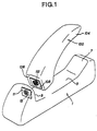
Fig. 1 to Fig. 4 show one embodiment of the noncontact
charging device according to the present invention. In the
figures, the reference numeral 1 indicates a charger, and the
reference numeral 100 indicates a cordless handset (sometimes
described as a handset unit hereinafter) of a telephone set
as a cordless equipment.
The charger 1 has an outer casing 5 with a handset unit
mounting base 3 on which the handset unit 100 is placed. The
outer casing 5 comprises a inclined pillow section 7 on which
a head section 104 of the outer casing 102 of the handset unit
100 is mounted, and an electromagnetic induction surface
section 9, and when the head section 104 is placed on the
inclined pillow section 7, a bottom surface section 106 of the
outer casing 102 faces to and contacts a electromagnetic
induction surface section 9, and the handset unit 100 is
positioned and set on the handset unit mounting base 3.
A printed board 11 is fixed and set with an engaging claw
13 on an internal surface of the electromagnetic induction
surface section 9 of the charger 1. On a surface of the printed
board 11 (a surface in the side of the electromagnetic induction
surface section 9), as well shown in Fig. 4, a conductor 14
is spirally patterned, and a pattern inductor, in other words
a primary side induction coil 15 having a spiral form comprising
a sheet coil is planarly formed with the conductor 14.
A sheet coil face (surface) of the printed board 11
uniformly contacts and joints to the entire internal surface
of the electromagnetic induction surface section 9 when set
on the electromagnetic induction surface section 9 of the
printed board 11 with the engaging claw 13. This feature is
very important for maintaining a gap between coils at an
appropriate value during mutual induction described later.
A capacitor 17 is mounted on a rear surface of the printed
board 11. This capacitor 17 is connected, as shown in Fig. 3,
in parallel to the primary side induction coil 15, and forms
an LC parallel resonance circuit in the primary side together
with the primary side induction coil 15. A high-frequency
power 19 is connected to the LC parallel resonance circuit in
the primary side.
The printed board 108 is seated on the internal surface
of the bottom surface section 106 of the handset unit 100 with
the engaging claw 110. A conductor is spirally patterned on
a surface on the printed board 108 (on a surface of the side
of the bottom surface 106) like in the printed board 11, and
with the conductor, a pattern inductor, in other words, a
secondary side induction coil 112 having a spiral form
comprising a sheet coil is formed on the surface.
A sheet coil face (surface) of the printed board 108 is
seated on the bottom surface section 106 of the printed board
108 with the engaging claw 110 and uniformly contacts and joints
to the entire internal surface of the bottom surface section
106. Also this feature is one of the important requirements
for maintaining a gap between coils at an appropriate value
during mutual induction described later.
A capacitor 114 is mounted on a rear surface of the
printed board 108. This capacitor 114 is connected in parallel
to the secondary side induction coil 112, and forms an LC
parallel resonance circuit in the secondary side together with
the secondary side induction coil 112. A secondary battery
118 to be charged is connected via a diode 116 to the LC parallel
resonance circuit in the secondary side.
In this configuration, when the handset unit 100 is
positioned and set on the handset unit mounting base 3 of the
charger 1, the bottom surface section 106 of the outer casing
102 faces to and contacts flat to the electromagnetic induction
surface section 9, and for this reason in the state where a
handset unit has been set, the primary side induction coil 15
and the secondary side induction coil 12 face in parallel to
each other with the electromagnetic induction surface section
9 of the outer casing 5 and the bottom surface section 106 of
the outer casing 102 therebetween, so that a gap between the
primary side induction coil 15 and the secondary side induction
coil 112 is inevitably decided by a total of wall thickness
of the electromagnetic induction surface section 9 and that
off the bottom surface section 106.
With this feature, only by setting wall thickness of the
electromagnetic induction surface section 9 and that of the
bottom surface section 106 to appropriate values respectively,
it is possible to accurately set a gap between the primary side
induction coil 15 and the secondary side induction coil 112
to a value at which the critical connection state can be
achieved.
With the configuration described above, a double tuning
circuit is formed with a combination of LC parallel resonance
circuits formed in the charger 1 and the handset unit 100
respectively, and power transmission from the charger 1 to the
handset unit 100 is executed by means of mutual induction by
the double tuning circuit.
As each of the primary side induction coil 15 and the
secondary side induction coil 112 is formed with a sheet coil,
construction of the coil itself and mounting construction for
the coil do not become complicated, and with the induction coils,
mutual induction is efficiently performed with a large
magnetic connection area with an appropriate gap at which the
critical connection state can be achieved and without making
larger size and weight of the coil.
Especially in a double tuning circuit based on a
combination of the LC parallel resonance circuits, the
critical connection state is achieved depending on the
magnetic connection coefficient, so that, by setting a gap
between the primary side induction coil 15 and the secondary
side induction coil 112 to on appropriate value, the critical
connection state can be obtained, and efficient power
transmission can be performed with the maximum and single peak
frequency characteristics.
Fig. 5 shows the inter-coil gap/loss level
characteristics for the harmonic frequency. This graph shows
that, in a case where the inter-coil gap is 6 mm, the loss level
is minimum with excellent mutual induction state, and that,
in a case where the inter-coil gap is more than or less than
6 mm, the loss level increases with the mutual induction state
degraded.
Accordingly, in this case, the appropriate gap enabling
the critical connection state is 6 mm, and wall thickness of
the electromagnetic induction surface section 9 and that of
the bottom surface section 106 should be set to 3 mm
respectively.
Sheet coils of the primary side induction coil 15 and
the secondary side induction coil 112 respectively are
spirally patterned on surfaces of the printed boards 11 and
108, so that a large planary magnetic field in obtained with
a small space and a large magnetic connection area can be
obtained without making larger size and weight of the coils.
With the features described above, efficient power
transmission is performed with little wasteful power
consumption.
Further this sheet coil is formed with a pattern inductor
provided on a printed board, and the pattern inductors are
mass-produced with stable performance and low cost by making
use of the printed board production technology, so that the
sheet coil, in other words, the primary side induction coil
15 and secondary side induction coil 112 are formed with low
cost products with stable quality, which allows cost
reduction.
Fig. 6 shows electric circuits in a noncontact charger
as well as in a cordless equipment (handset unit). It should
be noted that the same reference numerals as those used in Fig.
1 to Fig. 3 are assigned to portions corresponding to those
in Fig. 1 to Fig. 3.
The noncontact charger 1 comprises an LC parallel
resonance circuit 21 formed with a primary side induction coil
15 (L1) and a capacitor 17 (C2), a DC current source 23 obtained
from, for instance, an AC adapter, an oscillation circuit 25
comprising, for instance, a CR oscillator, a resonance circuit
driving transistor 27 (Q1) for driving the LC parallel
resonance circuit 21 at a high frequency when a high-frequency
signal outputted from the oscillation circuit 25 is given to
a gate terminal, a resonance state switching transistor 31 (Q2)
for switching a oscillation voltage level in the LC parallel
resonance circuit 21 between a high level and a low level by
opening and closing a circuit for a partial voltage resistance
29 (R21), a detection circuit 33 (D1, C5, R6) connected to the
LC parallel resonance circuit 21 and outputting amplitude of
an oscillation frequency signal as a voltage signal Va, a
variable amplifier 35 for amplifying an output voltage Va from
the detection circuit 33, and a comparator 37 (OP2, R11 to R14)
comparing a voltage Vb amplified by the variable amplifier 35
to a reference voltage Vref for comparison.
When the voltage Vb amplified by the variable amplifier
35 is larger than the reference value Vref for comparison, the
comparator 37 determines that the primary side induction coil
15 is not in the mutual conduction state, and outputs an ON
signal, and otherwise, namely when the voltage Vb is not larger
than the reference value Vref for comparison, the comparator
37 determines that the primary side induction coil is in the
mutual induction state, and outputs an OFF signal.
When outputted from the comparator 37, the ON or OFF
signal described above, namely a determination signal (output
voltage) Vc is inputted via a delay circuit 43 comprising a
resistance 39 (R20) and a capacitor 41 (C5) into a gate terminal
of the resonance state switching transistor 31.
When the primary side induction coil 15 is not in the
mutual induction state, namely in the idle state where the
handset unit 100 has not been set in the charger 1, the resonance
state switching transistor 31 is set in the ON state, sets a
oscillation voltage level in the LC parallel resonance circuit
21 to a low level, while, when the primary side induction coil
15 is in the mutual induction state, namely in the state where
the handset unit 100 has been set in the charger 1, the
transistor 31 is set in the OFF state, and sets a oscillation
voltage level in the LC parallel resonance circuit 21 to a high
level.
The variable amplifier 35 in this embodiment comprises
a non-inverting amplifier which is an operating amplifier (OP1),
has a partial voltage resistance 49 (R18) selectively connected
by a transistor 47 (Q3) to any of the offset voltage circuit
45 (R15 to R19), and selectively lowers the offset voltage Vd
with this partial voltage resistance 49.
The above-described ON/OFF signal (Vc) outputted from
the comparator 37 is given to a gate terminal of the transistor
47. With this feature, in the idle state where the handset
unit 100 is not set in the charger 1, the transistor 47 is set
in the ON state, and the offset voltage Vd becomes lower than
that during mutual inductance (in the state where the handset
unit 100 is set in the charger 1).
Also provided in a return resistance circuit 51 (R7 to
R10) of the variable amplifier 35 is a partial voltage
resistance 55 (R9) selectively connected by a transistor 53
(Q4) to the circuit, and the amplification factor G is
selectively made larger by this partial voltage resistance 55.
The above-described ON/OFF signal (Vc) outputted from
the comparator 37 is given to a gate terminal of the transistor
53. With this feature, in the idle state where the handset
unit 100 is not set in the charger 1, the transistor 53 is set
in the ON state, and the amplification factor G of the variable
amplifier 35 becomes larger than that in the mutual induction
state (in the state where the handset unit 100 is set in the
charger 1).
The handset unit 100 has a an LC parallel resonance
circuit 120 comprising a secondary side induction coil 112 (L2)
and a capacitor 114 (C7), a secondary battery 118, and a double
voltage rectification circuit 130 comprising two diodes 122
(D2), 124 (D3) mutually-inversively connected to each other and
provided between the resonance circuit 120 and the secondary
battery 118 and two smoothing capacitors 126 (C9) and 128 (C8).
It should be noted that, in Fig. 6, signs R1 to R22 indicate
a resistance respectively, C1 to C6 indicate a capacitor, Q1
to Q4 indicates a transistor respectively, and D1 to D3 indicates
a diode respectively.
Next description is made for operations of the noncontact
charger 1 and handset unit 100 each having the circuit as
described above with reference to the timing chart shown in
Fig. 7.
In the idle state (in the state where the handset unit
100 has been removed from the charger 1), an output signal Vc
from the comparator 37 is at a high level (ON signal), and each
of the transistors 31, 47, 53 is ON. Accordingly, in this state,
an oscillation level in the resonance circuit 21 is lowered
down to, for instance, around 6 Vp-p, an output voltage Va from
the detection circuit 33 is around 1.4 V, an offset voltage
Vd in the variable amplifier 35 is lowered to around 1.4 V,
the amplification factor G on the variable amplifier 35 is
lowered to around 7.5, an output voltage Vb from the variable
voltage is 4.2 V because Vb = Va (3 + G) - G · Vd, the comparison
value for reference Vref = 1.7 V, so that Vb is larger than
Vref and the output signal Vc from the comparator 37 is
maintained at a high level (3.8 V).
As described above, in the idle state, a oscillation
level in the resonance circuit 21 is lowered, so that, even
if a metallic conductor is placed by mistake on the charger
1, substantial induction heating does not occur and wasteful
power consumption is lowered.
In this state, when the handset unit 100 is set on the
charger 1, mutual induction is started by a double tuning
circuit comprising the resonance circuit 21 in the charger 1
and the resonance circuit 120 in the handset unit 100 in the
low level oscillation state, and power transmission from the
charger 1 to the handset unit 100 is started.
In the handset unit 100, because of existence of the
double voltage rectification circuit 130, a voltage between
terminals of the secondary battery 118 looks like 1/2 of the
actual value when viewed from the input side, and with this
feature, even if the oscillation level is low as described above,
when the handset unit 100 is set on the charger, a charging
current flows without fail.
With this feature, oscillation amplitude, namely
oscillation level in the resonance circuit 21 further lowers
to, for instance, around 1 Vp-p. Then an output voltage Va
from the detection circuit 33 is around 1.0 V, an output voltage
Vb from the variable amplifier 35 is 0 V because Vb = Va (3+G)
- G · Vd, a reference value for comparison Vref = 1.75 V
indicating that Vb < Vref, and an output signal Vc from the
comparator 37 is at a low level (0 V).
As a result, each of the transistors 47, 53 is immediately
turned OFF with the offset voltage Vd in the variable amplifier
35 raised to around 4 V, and the amplification factor G of the
variable amplifier 35 is lowered to around 3 V.
When state switching of the variable amplifier 35 as
described above is finished and an output state from the
variable amplifier 35 has been stabilized, an output signal
Vc (0 V) from the comparator 37 is inputted into the resonance
state switching transistor 31 under the delaying effect by the
delay circuit 43, and the transistor 31 is turned OFF. With
this operation, an oscillation level in the resonance circuit
21 is raised to around 10 Vp-p. Then an output voltage Va from
the detection circuit 33 goes up to around 3 V.
In this state, however, an offset voltage Vd in the
variable amplifier 35 is raised to around 4 V, and also the
amplification factor G of the variable amplifier 35 has been
lowered to around 3 V, so that the output voltage Vb from the
variable amplifier 35 is 0 V because Vb = Va (1+ G) - G ·
Vd, while the reference value for comparison Vref is 1. 75 V,
so that the relation of Vb < Vref is maintained, and an output
signal Vc from the comparator 37 is maintained at a low level
(0 V).
In this state, when the handset unit 100 is removed from
the charger 1, load is eliminated, and an oscillation level
in the resonance circuit 21 is raised to, for instance, around
17 Vp-p. In this state, an output voltage Va from the detection
circuit 33 goes up to around 5 V, an output voltage Vb from
the variable amplifier 35 is 8 V because Vb = Va (1 + G) - G ·
Vd, while the reference value for comparison Vref is 1.75 V
and Vb is larger than Vref (Vb > Vref), and an output signal
Vc from the comparator 37 is changed to a high level (3.8 V).
Then, the original idle state is restored.
With the configuration as described above, an offset
voltage in the variable amplifier 35 is switched according to
whether an oscillation voltage level in the resonance circuit
21 is a high level or a low level, and with only one reference
value for comparison Vref for the comparison 37, irrespective
of whether an oscillation voltage level in the resonance
circuit 21 is a high level or a low level, whether the primary
side induction coil 15 is in the mutual induction state or not,
namely whether the handset unit 100 is set on the charger 1
or not can accurately be determined.
Also an amplification factor for the variable 35
amplifier in a state other than the mutual induction state is
made larger as compared to that in the mutual induction state,
so that an output voltage from the variable amplifier largely
changes in response to change in oscillation amplitude, and
in the idle state where mutual induction state is not effected
and an oscillation voltage level in the resonance circuit is
at a low level, even if change in oscillation amplifier changes
only a little when the handset unit 100 is set in the charger
1, the fact that the handset unit 100 has been set can accurately
be detected by the comparator 37.
With the features as described above, whether the handset
unit 100 has been set in the charger 1 or not can accurately
be detected without requiring any specific sensor.
Fig. 8 shows an electric circuit according to another
embodiment of the noncontact charger and cordless equipment
(handset unit) according to the present invention. It should
be noted that, in Fig. 8, the same reference numerals are
assigned to portions corresponding to those in Fig. 6 and
description thereof is omitted herein.
An output voltage Va from the detection circuit 33 in
each state is the same as that in the embodiment described above,
and this output voltage Va is inputted into a first comparator
61 as well as into a second comparator 63.
The first comparator 61 compares an output voltage Va
to the first reference value for comparison Vref1, and outputs
a low signal when Va is larger than Vref1 (Va > Vref1), and
otherwise outputs a high signal. As the first reference value
for comparison Vref1 is set to around 1.2 V, the first
comparator 61 outputs a high signal only when the handset unit
100 is set on the charger 1 in the idle state, and outputs a
low signal in the idle state, when charging with a high level
output, and when the handset unit 100 is removed from the
charger 1 in the charging state with a high level output.
The second comparator 63 compares the output voltage Va
to a second reference value for comparison Vref2 larger than
the first reference value for comparison Vref1, and when Va
is larger than Vref2 (Va > Vref2), outputs a low signals, and
otherwise output a high signal. As the second reference value
for comparison Vref2 is set to around 4 V, the second comparator
63 outputs a low signal only when the handset unit 100 is removed
from the charger 1 in the charging state with high level output,
and outputs a low signal, when the handset unit 100 is set in
the charger 1 in the idle state, or when charging is executed
with high level output.
Output signals from the first comparator 61 and second
comparator 63 are inputted to a two-input type of NOR gate 65
and an AND gate 76 respectively. An output signal from the
NOR gate 65 is inputted into a reset terminal of the D-latch
circuit 69, and an output signal from the AND gate 67 is inputted
to a clock terminal of the D-latch circuit 69. The D-latch
circuit 69 inverts an inverted Q output signal from ON to OFF
according to shift of a signal inputted into the clock terminal
from low to high, and also inverts the inverted Q output signal
from OFF to ON according to reset input. This inverted Q output
signal is inputted to a gate terminal of the resonance state
switching transistor 31 as a determination signal indicating
whether the primary side induction coil 15 is in the mutual
induction state or not.
For this reason, also in this embodiment, when the
handset unit 100 is set in the charger 1 in the idle state,
an output signal from the NAD gate 67 goes high, while a signal
inputted into the clock terminal changes from low to high, so
that the inverted Q output signal is inverted from ON to OFF
and the resonance state switching transistor 31 is turned OFF,
With this feature, an oscillation level in the resonance
circuit 21 changes from low level output to high level output.
In contrast, when the handset unit 100 is removed from
the charger 1 in the charging state with high level output,
an output signals from the NAND gate 65 goes high, and the
inverted Q output signal is inverted from OFF to ON according
to reset input, and the resonance state switching transistor
31 is turned ON. With this operation, an oscillation level
in the resonance circuit 21 is changed from high level output
to low level output.
For the reasons described above, also in this embodiment,
an oscillation level in the resonance circuit 21 lowers in the
idle state, so that, even if a metallic conductor is placed
by mistake on the charger 1, substantial induction heating does
not occur with wasteful power consumption reduced, and whether
the handset unit 100 has been set in the charger 1 or not can
accurately be detected without requiring any specific sensor.
As understood from the description above, in the
noncontact charging device according to the present invention,
each of the primary side induction coil and secondary side
induction coil provided in a charger and a cordless equipment
respectively comprises a sheet coil, so that construction of
the coil itself and the mounting construction thereof are not
complicated, and with the induction coils, mutual induction
is efficiently executed with a appropriate gap and a large
magnetic connection area without making size and weight of the
coil larger, and wasteful power consumption is reduced and
charging is executed at a high speed.
In the non-contact charging device according to the
present invention, by setting a gap between the primary side
induction coil and secondary side induction coil to an
appropriate value, the critical connection state is achieved
and efficient power transmission is executed with the maximum
and signal peak frequency characteristics, and also with this
feature, wasteful power consumption is reduced and charging
is executed at a high speed.
In the noncontact charging device according to the
present invention, a sheet coil is spirally patterned on one
plane, so that a large and flat magnetic field is obtained with
a small space and a large magnetic connection area is obtained
without making larger size and weight of each coil, and also
with this feature, wasteful power consumption is reduced and
charging is executed at a high speed.
In the noncontact charging device according to the
present invention, a sheet coil comprises a pattern inductor
patterned on a printed board, and as pattern inductors can be
mass-produced with stable performance and high productivity
and also with low cost, the sheet coil can comprises a low cost
product with excellent and stable quality.
The charger according to the present invention functions
as the noncontact charger according to the present invention,
so that wasteful power consumption is reduced and charging is
executed at a high speed.
The cordless equipment according to the present
invention functions as a cordless equipment in the noncontact
charging device according to the present invention, so that
wasteful power consumption is reduced and charging is executed
at a high speed.
In the noncontact charger according to the present
invention, when a cordless equipment is set in the charger,
mutual induction state is detected by the mutual induction
state detecting means and an oscillation voltage level in the
resonance circuit is set by the resonance state switching means
to a high level, and if a cordless equipment is not set in the
charger, the mutual induction state detecting means detects
that the mutual induction state has not been effected, and a
oscillation voltage level in the resonance circuit is set by
the resonance state switching means to a low level, so that,
even if a metallic conductor is placed by mistake on the charger
in the idle state which is different from the mutual induction
state, substantial induction heating does not occur with
wasteful power consumption reduced, and whether any cordless
equipment is placed on the charger or not can accurately be
detected without requiring any specific sensor.
In the noncontact charger according to the present
invention, an offset voltage in the variable amplifier is
switched according to whether a oscillation voltage level in
the resonance circuit is at a high level or a low level, so
that, even with only one reference value for comparison,
whether the primary side induction coil is in the mutual
induction state or not can accurately be determined
irrespective of whether a oscillation voltage level in the
resonance circuit is high or low.
In the noncontact charger according to the present
invention, a determination signal is given to the variable
amplifier, and an amplification factor for the variable
amplifier in a state other than the mutual induction state is
made larger as compared to that in the mutual induction state,
so that even if oscillation amplitude changes only a little
when a cordless equipment is set in the charger in the idle
state where a cordless equipment is not set in the charger,
the fact that the cordless equipment has been set can accurately
be detected by the compactor.
In the noncontact charger according to the present
invention, input of a determination signal into the
oscillation state switching means is delayed by the delay
circuit, and switching of oscillation state is performed after
output state of the variable amplifier has been stabilized,
so that hunting never occurs and an operation for switching
the oscillation state is executed under stable conditions.
In the noncontact charger according to the present
invention, a determination signal indicating whether the
induction coil is in the mutual induction state or not is
outputted with a combination of output signals from the first
comparator and second comparator, and for this reason whether
a cordless equipment has been set on the charger or not can
accurately be detected without requiring any specific sensor.
In the cordless equipment according to the present
invention, a voltage between terminals of the secondary
battery seems to be 1/2 of the actual value when viewed from
the input side because of existence of the double voltage
rectification circuit, so that, even if an oscillation level
in the stand-by state is low, a charging current flows without
fail when a cordless equipment is set in the charge, and the
fact that the cordless equipment has been set in the charger
can accurately be detected in the charger side according to
change in oscillation amplitude.
This application is based on Japanese patent application
No. HEI 8-173976 filed in the Japanese Patent Office on July
3, 1996, the entire contents of which are hereby incorporated
by reference.
The invention may e.g. be summarized as follows:
Capacitors are connected in parallel to a primary side
induction coil in a charger 1 and a secondary side induction
coil in a cordless equipment (handset unit) respectively, and
LC parallel resonance circuits are formed in the charger and
the cordless equipment respectively with this parallel
connection. Each of the primary side induction coil and
secondary side induction coil is formed with a sheet coil, and
the sheet coils are arranged and fixed in the charger and the
cordless equipment respectively so that the sheet coils face
to each other with a prespecified gap in the charging state
where the cordless equipment has been set in the charger.