The present invention relates to improved IC package, IC prober and
connector as well as method of fabricating the same.
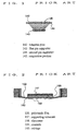
FIG. 1 is a schematic view illustrative of a conventional tungsten probe
comprising a large number of tungsten pins 142, which are supported by a
first supporter 143 at a first side and by a second supporter 145 at a second
side. The tungsten pins 142 are aligned so as to have a first pitch at the first
side and a second pitch at the second side wherein the first pitch is much
smaller than the second pitch. The pitch of the tungsten pins 142
remarkably increases toward the second side from the first side. The first
pitch of the tungsten pins 142 at the first side is 100 micrometers, whilst the
second pitch of the tungsten pins 142 at the second side is a few
millimeters which is larger by 20-30 times than the first pitch.
The above tungsten probe has the following disadvantages. Each of the
tungsten pins 142 has a relatively large length. This causes a deterioration
in high frequency performance of the tungsten probe. Since it is required to
form each pin separately, this causes increase in manufacturing cost.
Further, since the second pitch of the tungsten pins is much wider than the
first pitch, a large number of the tungsten pins 142 leads to the problem
with spatial limitation.
FIG. 2 is a cross sectional elevation view illustrative of a membrane probe
which comprises a polyimide film 156, an elastomer 158 which is provided
on a first surface of the polyimide film 156, a supporting substrate 157
provided on the elastomer 158, contacts 159 provided on a second surface
of the polyimide film 156 and wirings 160 which extend over the second
surface of the polyimide film 156 from the contacts outwardly.
The above membrane probe also has the following problem. It is difficult to
obtain contacts with all of the terminals on an area of 10cm × 10cm or more
due to a difference in level between the wafer and probe. It is also difficult
to form a large number of wirings connected to a large number of pins due
to a limited wiring area. This means it difficult to obtain connections
between the probe card and the external device.
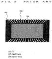
FIG. 3 is a schematic plane view illustrative of a conventional DIP mold
package which comprises an IC 162, lead frames 163 extending from the
IC package 162 outwardly and connected via wire-bonding to the IC 162
and an epoxy resin 164 molding the IC 162 and the lead frames 163.
The above conventional DIP mold package has the following disadvantages.
It is difficult to provide external electrodes in the form of ball grid array in
the structural viewpoint. If the IC is assembled into the package by a flip-chip
bonding method, it is required to form bumps on the IC or substrate or
supply solders. This results in increased numbers of the fabrication
processes and also increased manufacturing cost. In view of the assembly, a
pitch of the electrodes of the package is required to be 500 micrometers or
more, for which reason in order to increase the number of electrodes of the
IC, it is required to enlarge a package size.
In order to reduce the package size, it was proposed to combine a chip size package with the
ball grid array. Notwithstanding, the wire-bonding, ball bumps and solders are also
required.
Accordingly, it is an object of at least the preferred embodiments of the
present invention to provide a novel IC package free from the above
disadvantages.
The present invention provides an IC package comprising an IC chip
substrate having a surface on which a plurality of electrodes are
formed, and an organic substrate having a first surface on which a plurality
of bump electrodes are provided.
Each of the bump electrodes is in contact with a
corresponding one of the electrodes on the IC chip substrate. The organic
substrate has a plurality of through holes and metallization patterns
electrically connecting each of the bump electrodes to a corresponding one of
the through holes.
It is preferable that a space between the IC chip substrate and the organic
substrate is filled with a sealing resin material.
It is also preferable that each of the bump electrodes has a pyramidal shape.
It is also preferable that each of the bump electrodes comprises a bump
body which is made of the same material as the organic substrate and a
metal film coating the bump body.
It is also preferable that the bump electrodes are aligned to form a rectangle
having four sides, each of which comprises an alignment of the bump
electrodes, the through holes are aligned outside and along the each side of
the rectangle of the bump electrodes and the through holes are distanced
from the bump electrodes and the metallization patterns provide electrical
connections between each of the bump electrodes and the corresponding
one of the through holes.
It is also preferable that the bump electrodes are aligned in matrix, the
through holes are also aligned in matrix so that each of the through holes is
positioned adjacent to the corresponding one of the bump electrodes and
the metallization patterns provide electrical connections between each of
the bump electrodes and the corresponding one of the through holes. In this
case, it is more preferable that the organic substrate has a second surface on
which ball grid arrays are provided at positions corresponding to the bump
electrodes so that the ball grid arrays are aligned in matrix and each of the
through holes is positioned adjacent to the corresponding one of the ball
grid arrays and metallization patterns are further formed on the second
surface of the organic substrate so as to provide electrical connections
between each of the ball grid arrays and the corresponding one of the
through holes.
It is also preferable that the organic substrate is made of ABS resin.
It is also preferable that the organic substrate is made of liquid crystal
polymer resin.
It is also preferable that the organic substrate is made of elastomer.
The present invention also provides an IC probe card comprising a
multilevel interconnection substrate, and a plurality of organic substrates
provided on the multilevel interconnection substrate. Each of the organic
substrates has a surface on which a plurality of bump electrodes are
provided.
Each of the bump electrodes is in contact with a corresponding one of the
electrodes on the IC chip substrate. The organic substrate has a plurality of
through holes and metallization patterns electrically connecting each of the
bump electrodes to a corresponding one of the through holes.
It is preferable that a space between the IC chip substrate and the organic
substrate is filled with a sealing resin material.
It is also preferable that each of the bump electrodes has a pyramidal shape.
It is also preferable that each of the bump electrodes comprises a bump
body which is made of the same material as the organic substrate and a
metal film coating the bump body.
It is also preferable that the bump electrodes are aligned to form a rectangle
having four sides, each of which comprises an alignment of the bump
electrodes, the through holes are aligned outside and along the each side of
the rectangle of the bump electrodes and the through holes are distanced
from the bump electrodes and the metallization patterns provide electrical
connections between each of the bump electrodes and the corresponding
one of the through holes.
It is also preferable that the bump electrodes are aligned in matrix, the
through holes are also aligned in matrix so that each of the through holes is
positioned adjacent to the corresponding one of the bump electrodes and
the metallization patterns provide electrical connections between each of
the bump electrodes and the corresponding one of the through holes. In this
case, it is more preferable that the organic substrate has a second surface on
which ball grid arrays are provided at positions corresponding to the bump
electrodes so that the ball grid arrays are aligned in matrix and each of the
through holes is positioned adjacent to the corresponding one of the ball
grid arrays and metallization patterns are further formed on the second
surface of the organic substrate so as to provide electrical connections
between each of the ball grid arrays and the corresponding one of the
through holes.
It is also preferable that the organic substrate is made of ABS resin.
It is also preferable that the organic substrate is made of liquid crystal
polymer resin.
It is also preferable that the organic substrate is made of elastomer.
The present invention also provides a connector for electrically connecting
first electrode arrays on a first substrate and second electrode arrays on a
second substrate. The connector comprises an organic substrate having a
first surface on which first bump electrode arrays are provided and a
second surface on which second bump electrode arrays are provided. The
organic substrate is sandwiched between the first and second substrates so
that each of the first bump electrode arrays is in contact with a corresponding
one of the first electrode arrays on the first substrate whilst each of the
second bump electrode arrays is in contact with a corresponding one of the
second electrode arrays on the second. The organic substrate has a plurality
of through holes and metallization patterns electrically connecting each of
first bump electrode arrays through corresponding one of the through holes
to corresponding one of the second bump electrode arrays.
It is preferable that each bump of the first and second bump arrays has a
pyramidal shape.
It is also preferable that each of the bump electrodes comprises a bump
body which is made of the same material as the organic substrate and a
metal film coating the bump body.
It is also preferable that each of the first and second bump arrays are
aligned to form a rectangle having four sides, each of which comprises an
alignment of bump electrodes, the through holes are aligned outside and
along the each side of the rectangle of the bump electrodes and the through
holes are distanced from the bump electrodes and the metallization patterns
provide electrical connections between each of the bump electrodes and
corresponding one of the through holes.
It is also preferable that bump electrodes of each of the first and second
bump arrays are aligned in matrix, the through holes are also aligned in
matrix so that each of the through holes is positioned adjacent to the
corresponding one of the bump electrodes and the metallization patterns
provide electrical connections between each of the bump electrodes and the
corresponding one of the through holes.
It is also preferable that the organic substrate is made of ABS resin.
It is also preferable that the organic substrate is made of liquid crystal
polymer resin.
It is also preferable that the organic substrate is made of elastomer.
The present invention also provides a method of forming an IC package
comprising the following steps. A surface of a silicon wafer is
selectively subjected to an etchant for selectively etching the silicon
substrate so that pits are formed in the surface of the silicon wafer. A
pin die having a plurality of pins is assembled on the surface of the
silicon wafer so that the pits face the pin die and the pins extend between
the pin die and the surface of the silicon wafer. An injection molding
of an organic resin material is carried out by use of the pin die combined on
the silicon wafer to form an organic substrate having a surface on
which bumps made of the same material as the organic substrate are formed
at the corresponding positions to the pits. The organic substrate has through
holes at the corresponding positions as the pins. A photo-resist pattern is
provided which extends over the organic substrate. The organic substrate is
subjected to an electroless plating of a metal to selectively form
metallization patterns, each of which extends from the bump to
corresponding one of the through holes. The photo-resist film is removed
from the organic substrate. A photo-sensitive epoxy resin pattern is
provided which extends over the organic substrate except over the bumps.
The bumps are subjected to a metal pleating to form a metal plating film
which coats the bumps. An IC chip with electrodes which have been metal-plated
is placed on the organic substrate for bonding the same. A space
between the IC chip and the organic substrate is filled with a sealing resin
material for subsequent curing the sealing resin material by a heat
treatment.
The present invention provides a method of forming an IC probe card
comprising the following steps. A surface of a silicon wafer is
selectively subjected to an etchant for selectively etching the silicon
substrate so that pits are formed in the surface of the silicon wafer. A
pin die having a plurality of pins is assembled on the surface of the
silicon wafer so that the pits face to the pin die and the pins extend between
the pin die and the surface of the silicon wafer. An injection molding
of an organic resin material is carried out by use of the pin die combined on
the silicon wafer to form an organic substrate having a surface. on
which bumps made of the same material as the organic substrate are formed
at the corresponding positions to the pits. The organic substrate has through
holes at the corresponding positions as the pins. A photo-resist pattern is
provided which extends over the organic substrate. The organic substrate is
subjected to an electroless plating of a metal to selectively form
metallization patterns, each of which extends from the bump to
corresponding one of the through holes. The photo-resist film is removed
from the organic substrate. A photo-sensitive epoxy resin pattern is
provided which extends over the organic substrate except over the bumps.
The bumps are subjected to a metal pleating to form a metal plating film
which coats the bumps. At least one of the organic substrates is placed on a
multilevel interconnection substrate.
The present invention provides a method of forming an connector
comprising the following steps. A surface of a silicon wafer is
selectively subjected to an etchant for selectively etching the silicon
substrate so that pits are formed in the surface of the silicon wafer.
Two such silicon wafers are used for carrying out an injection molding of
an organic resin material to form an organic substrate having a first surface,
on which first bumps made of the same material as the organic substrate are
formed at the corresponding positions to the pits, and a second surface, on
which second bumps made of the same material as the organic substrate are
formed at the corresponding positions to the pits. Through holes are formed
in the organic substrate. A photo-resist pattern is provided which extends
over the organic substrate. The organic substrate is subjected to an
electroless plating of a metal to selectively form metallization patterns,
each of which extends from the first bump through corresponding one of
the through holes to corresponding one of the second bumps. The photo-resist
film is removed from the organic substrate. A photo-sensitive epoxy
resin pattern is provided which extends over the organic substrate except
over the bumps. The bumps are subjected to a metal pleating to fonn a
metal plating film which coats the bumps. The organic substrate is placed
between first and second glass epoxy substrates which have first and
second electrode arrays so that the first bumps formed on the first surface
of the organic substrate are in contact with the first electrode array of the
first glass epoxy substrate whilst the second bumps formed on the second
surface of the organic substrate are in contact with the second electrode
array of the second glass epoxy substrate for electrically connecting the
first electrode array to the second electrode array.
Preferred embodiments of the present invention will be described in detail
with reference to the accompanying drawings.
FIG. 1 is a schematic view illustrative of a conventional tungsten probe.
FIG. 2 is a cross sectional elevation view illustrative of a membrane probe.
FIG. 3 is a schematic plane view illustrative of a conventional DIP mold
package.
FIG. 4 is a schematic perspective view illustrative of a substrate formed
with etch pits in a first embodiment according to the present invention.
FIG. 5 is a fragmentary cross sectional elevation view illustrative of etch
pits formed on a top surface of a substrate in a first embodiment according
to the present invention.
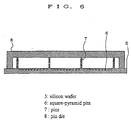
FIG. 6 is a fragmentary cross sectional elevation view illustrative of a die
assembly in a first embodiment according to the present invention.
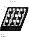
FIG. 7 is a schematic perspective view illustrative of a die assembly in a
first embodiment according to the present invention.
FIG. 8 is a schematic perspective view illustrative of an organic substrate in
a first embodiment according to the present invention.
FIG. 9 is a fragmentary plane view illustrative of an organic substrate in a
first embodiment according to the present invention.
FIG. 10 is a cross sectional elevation view illustrative of square-pyramid
bumps aligned on an organic substrate in a first embodiment according to
the present invention.
FIG. 11 is a fragmentary cross sectional elevation view illustrative of a
connector in a first embodiment according to the present invention.
FIG. 12 is a fragmentary plane view illustrative of a first surface of an
organic substrate with area bumps aligned in 16x16 matrix over the
organic substrate in second and third embodiments according to the present
invention.
FIG. 13 is a fragmentary plane view illustrative of a second surface of an
organic substrate with area bumps aligned in 16x16 matrix over the
organic substrate in second and third embodiments according to the present
invention.
FIG. 14 is a fragmentary plane view illustrative of IC probes formed on a
multilevel interconnection substrate in fourth and fifth embodiments
according to the present invention.
FIG. 15 is a fragmentary cross sectional elevation view illustrative of first
and second square-pyramid bumps arrays formed on both first and second
surfaces of an organic substrate in sixth, seventh and eighth embodiments
according to the present invention.
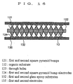
FIG. 16 is a fragmentary cross sectional elevation view illustrative of a
connector which comprises an organic substrate having first and second
surfaces on which first and second square-pyramid bumps arrays are
formed respectively and first and second glass epoxy substrates having first
and second electrode arrays which are in contact with the first and second
square-pyramid bumps arrays respectively in sixth, seventh and eighth embodiments
according to the present invention.
A first embodiment according to the present invention will be described with reference to
Figures 4 to 11.
As illustrated in FIG. 4, a silicon wafer 5 was prepared which has first and
second surfaces coated with silicon dioxide films. The silicon wafer 5 has a
diameter of 6 inches and a thickness of 1 millimeter. A photo-resist is
applied on the silicon wafer 5 and then patterned to form a photo-resist
pattern on the silicon wafer 5. By use of the photo-resist pattern, patterns of
openings 38 are formed in the silicon wafer 5 so that the openings are
aligned in the form of rectangles which are aligned in matrix separately
from each other at a small distance wherein each rectangle has four sides
each of which comprises an alignment of the openings. The silicon wafer is
then subjected to a hydrofluoric acid solution for 10 minutes. The used
photo-resist film is removed from the silicon wafer 5 before the silicon
wafer 5 is then subjected to a solution containing 30% of potassium
hydroxide for 30 minutes so that (111)-faces are shown and square-pyramid
pits 6 are formed in the first surface of the silicon wafer 5. Each of the pits
6 has an opening area of 100 µm × 100 µm at the first surface of the silicon
wafer 5 and a depth of 70.8 µm. The square-pyramid pits 6 are aligned in
the form of rectangles which are aligned in matrix separately from each
other at a small distance wherein each rectangle has four sides each of
which comprises an alignment of the square-pyramid pits 6.
As illustrated in FIG. 6, a pin die 8 is assembled on the first surface of the
silicon wafer 5 so that the square-pyramid pits 6 face to the pin die 8. Pins
7 are provided on the pin die 8 so that the pins 7 extend between the pin die
8 and the first surface of the silicon wafer 5. Each of the pins 7 has a
diameter of 0.3 millimeters and a length of 1 millimeters. The pins 7 are
aligned at a pitch of 0.5 millimeters. The pins 7 are aligned in the form of
rectangles which are aligned in matrix and bounded with each other
wherein each rectangle has four sides each of which comprises an
alignment of the pins 7. Each side of the rectangle extends between the
adjacent parallel sides of the rectangles of the pits 6. The pin die assembly
is used for an injection molding of ABS resin so that an organic substrate 2
is formed as illustrated in FIG. 8. The organic substrate 2 has through holes
3 at the same position as the pins 7 and square-pyramid bumps 1 at the
same position as the square-pyramid pits 6. The through holes 3 are aligned
along each side of the organic substrate 2. The square-pyramid pits 6 are
aligned inside the through holes. The existence of the pins 7 results in
formation of the through boles 3. Burrs are formed on the organic substrate
2 when the through holes 3 are formed. The burrs are removed by YAG
pulse laser. The organic substrate 2 has a thickness of 1 millimeter and a
size of 40mm × 40mm. Each square-pyramid bump 1 has a top slightly
rounded. The height of the square-pyramid bump 1 is 60 micrometers. The
square-pyramid bumps 1 are aligned at a pitch of 250 micrometers. A
surface of the organic substrate 2 is treated by a plasma asher for 5 minutes.
A photo-resist pattern is formed by a photo-lithography so that the photo-resist
pattern extends over the organic substrate 2 except over regions on
which no metallization nor wiring is intended to be made. The organic
substrate 2 is subjected to an electroless plating of copper to selectively
form metallization patterns 9, each of which extends from the square-pyramid
bump 1 to the corresponding through hole 3 as illustrated in FIG.
9. The metallization patterns 9 have a thickness of 10 micrometers. The
photo-resist film is removed from the surface of the organic substrate 2. A
photo-sensitive epoxy resin is applied on the organic substrate 2 and then
patterned so that the photo-sensitive epoxy resin pattern extends over the
organic substrate 2 except over the square-pyramid bumps 1. The square-pyramid
bumps 1 are subjected to a nickel plating and subsequent indium
50wt% - tin 50wt% plating to form laminations of a nickel plating film and
an indium 50wt% - tin 50wt% plating film which coat the square-pyramid
bumps 1. The organic substrate 2 is cut and divided into a plurality of
substrates, each of which has a single rectangle of the alignments of the
square-pyramid bumps 1 and the metallization patterns 9 extending from
the square-pyramid bumps 1 through the through holes 3. Each of the
substrates is illustrated in FIG. 10.
As illustrated in FIG. 11, an IC chip 25 with electrodes 27 which have been
nickel-plated and gold-plated is aligned on the organic substrate 2. The
combined IC chip 25 and the organic substrate 2 are then heated at 120°C
and pressed at 20g for each contact for bonding the same. A space between
the combined IC chip 25 and the organic substrate 2 is filled by a dispenser
with a sealing resin 26 which comprises 30wt% of epoxy resin and 70wt%
of silica filler. The combined IC chip 25 and the organic substrate 2 are
once heated at 150°C and then remain for 30 minutes to cure the sealing
resin 26. The heating causes melt indium-tin and gold to be inter-diffused
whereby a melting point of the metal is increased to prevent the melting of
the contact even heated for curing the sealing resin.
It was confirmed that of the IC package a resistance between the wiring of
the substrate to the electrode of the IC is extremely low, for example, 10m
Ω or less. The IC package was subjected to a thermal cycle test of 500
times between -40°C and 125°C. The IC package was not broken.
A second embodiment according to the present invention will be described
with reference to FIGS. 12 through 13.
A silicon wafer was prepared which has first and second surfaces coated
with silicon dioxide films. The silicon wafer has a diameter of 6 inches and
a thickness of 1 millimeter. A photo-resist is applied on the silicon wafer
and then patterned to form a photo-resist pattern on the silicon wafer. By
use of the photo-resist pattern, patterns of openings are formed in the
silicon wafer so that the openings are aligned in matrix at a constant pitch
over the silicon wafer. The silicon wafer is then subjected to a hydrofluoric
acid solution for 10 minutes. The used photo-resist film is removed from
the silicon wafer before the silicon wafer is then subjected to an alkyl
solution such as a solution containing 30% of potassium hydroxide for 30
minutes so that (111)-faces are shown and square-pyramid pits are formed
in the first surface of the silicon wafer. The square-pyramid pits are aligned
in matrix. A metal thin film is formed by sputtering method over the silicon
wafer. The silicon wafer is then subjected to a nickel plating to form a
nickel film having a thickness of 5 millimeters over the silicon wafer so
that the shapes of the pits are transcribed. By use of the nickel plated film
as a template, a mold releasing agent is applied and gold sputtering and
nickel plating are then carried out for preparation of a template of the
silicon wafer for the injection mold
A pin die is assembled on the first surface of the silicon wafer as one
template so that the square-pyramid pits face to the pin die. Pins are
provided on the pin die so that the pins extend between the pin die and the
first surface of the silicon wafer. Each of the pins has a diameter of 0.2
millimeters and a length of 1 millimeters. The pins are aligned in 16 × 16
matrix at the same pitch of 0.5 millimeters as the square-pyramid pits so
that each of the pins is positioned to be adjacent to one side of the
corresponding one of the square-pyramid pits. The pin die assembly is used
for an injection molding of ABS resin so that an organic substrate 92 of
10mm × 10mm is formed. As illustrated in FIG. 12, the first surface of the
organic substrate 92 has through holes 93 at the same position as the pins
and square-pyramid bumps 91 at the same position as the square-pyramid
pits. As illustrated in FIG. 13, the second surface of the organic substrate
92 has through holes 93 at the same position as the pins and ball grid arrays
94 at the same position as the square-pyramid pits. The through holes 93
are aligned in 16x16 matrix at a pitch of 0.5 millimeters. The square-pyramid
bumps 91 are also aligned in 16 × 16 matrix at the same pitch of
0.5 millimeters so that each of the through holes 93 is positioned adjacent
to one side of the corresponding one of the square-pyramid bumps 91. The
ball grid arrays 94 are also aligned in 16 × 16 matrix at the same pitch of
0.5 millimeters so that each of the through holes 93 is positioned adjacent
to one side of the corresponding one of the ball grid arrays 94. The
existence of the pins results in formation of the through holes 93. Burrs are
formed on the organic substrate 92 when the through holes 93 are formed.
The burrs are removed by YAG pulse laser. The organic substrate 92 has a
thickness of 1 millimeter and a size of 10mm × 10mm. Each square-pyramid
bump 91 has a top slightly rounded. Surfaces of the organic
substrate 92 are treated by a plasma asher for 5 minutes. Photo-resist
patterns are formed on both surfaces of the organic substrate 92 by a photo-lithography.
The organic substrate 92 is then subjected to an electroless
plating of copper to form copper plated films having a thickness of 10
micrometers. The organic substrate 92 is then subjected to an electroless
plating of nickel to form nickel plated films having a thickness of 2
micrometers. The organic substrate 92 is then subjected to an electroless
plating of gold to form gold plated films having a thickness of 0.5
micrometers. The used photo-resist films are removed from the first and
second surfaces of the organic substrate 92. A photo-sensitive epoxy resin
is applied on the first and second surfaces of the organic substrate 92 and
then patterned so that the photo-sensitive epoxy resin patterns extend over
both the first and second surfaces of the organic substrate 92 except over
the square-pyramid bumps 91 and the ball grid arrays 94. The square-pyramid
bumps 91 and the ball grid arrays 94 are subjected to a nickel
plating and subsequent indium 50wt% - tin 50wt% plating to form
laminations of a nickel plating film having a thickness of 2 micrometers
and an indium 50wt% - tin 50wt% plating film having a thickness of 10
micrometers which coat the square-pyramid bumps 91 and the ball grid
arrays 94.
An IC chip with electrodes which have been nickel-plated and gold-plated
is aligned on the organic substrate 92. The combined IC chip and the
organic substrate 92 are tben heated at 150°C and pressed at 20g for each
contact for bonding the same. A space between the combined IC chip 25
and the organic substrate 92 and spaces of the through holes are filled by a
dispenser with a sealing resin which comprises 30wt% of epoxy resin and
70wt% of silica filler. The combined IC chip and the organic substrate 92
are once heated at 150°C and then remain for 30 minutes to cure the
sealing resin. The heating causes melt indium-tin and gold to be inter-diffused
whereby a melting point of the metal is increased to prevent the
melting of the contact even heated for curing the sealing resin.
It was confirmed that of the IC package a resistance between the wiring of
the substrate to the electrode of the IC is extremely low, for example, 10m
Ω or less. The IC package was subjected to a thermal cycle test of 500
times between -40°C and 125°C. The IC package was not broken. The
external shape almost remains unchanged between 8mm × 8mm and 10mm
× 10mm. This means that the size reduction is possible. Since the ball grid
arrays 94 are aligned at a pitch of 0.5 millimeters in 16 × 16 matrix, the IC
package with 256 pins and small size is obtained.
A third embodiment according to the present invention will be described
with reference to FIGS. 12 through 13.
A silicon wafer was prepared which has first and second surfaces coated
with silicon dioxide films. The silicon wafer has a diameter of 6 inches and
a thickness of 1 millimeter. A photo-resist is applied on the silicon wafer
and then patterned to form a photo-resist pattern on the silicon wafer. By
use of the photo-resist pattern, patterns of openings are formed in the
silicon wafer so that the openings are aligned in matrix at a constant pitch
over the silicon wafer. The silicon wafer is then subjected to a hydrofluoric
acid solution for 10 minutes. The used photo-resist film is removed from
the silicon wafer before the silicon wafer is then subjected to an alkyl
solution such as a solution containing 30% of potassium hydroxide for 30
minutes so that (lll)-faces are shown and square-pyramid pits are formed
in the first surface of the silicon wafer. The square-pyramid pits are aligned
in matrix. A metal thin film is formed by sputtering method over the silicon
wafer. The silicon wafer is then subjected to a nickel plating to form a
nickel film having a thickness of 5 millimeters over the silicon wafer so
that the shapes of the pits are transcribed. By use of the nickel plated film
as a template, a mold releasing agent is applied and gold sputtering and
nickel plating are then carried out for preparation of a template of the
silicon wafer for the injection mold
A pin die is assembled on the first surface of the silicon wafer as one
template so that the square-pyramid pits face to the pin die. Pins are
provided on the pin die so that the pins extend between the pin die and the
first surface of the silicon wafer. Each of the pins has a diameter of 0.2
millimeters and a length of 1 millimeters. The pins are aligned in 16 × 16
matrix at the same pitch of 0.5 millimeters as the square-pyramid pits so
that each of the pins is positioned to be adjacent to one side of the
corresponding one of the square-pyramid pits. The pin die assembly is used
for an injection molding of ABS resin so that an organic substrate 92 of
10mm × 10mm is formed. The organic substrate 92 is polished to have a
thickness of 0.3 millimeters. As illustrated in FIG. 12, the first surface of
the organic substrate 92 has through holes 93 at the same position as the
pins and square-pyramid bumps 91 at the same position as the square-pyramid
pits. As illustrated in FIG. 13, the second surface of the organic
substrate 92 has through holes 93 at the same position as the pins and ball
grid arrays 94 at the same position as the square-pyramid pits. The through
holes 93 are aligned in 16×16 matrix at a pitch of 0.5 millimeters. The
square-pyramid bumps 91 are also aligned in 16×16 matrix at the same
pitch of 0.5 millimeters so that each of the through holes 93 is positioned
adjacent to one side of the corresponding one of the square-pyramid bumps
91. The ball grid arrays 94 are also aligned in 16 × 16 matrix at the same
pitch of 0.5 millimeters so that each of the through holes 93 is positioned
adjacent to one side of the corresponding one of the ball grid arrays 94. The
existence of the pins results in formation of the through holes 93. Burrs are
formed on the organic substrate 92 when the through holes 93 are formed.
The burrs are removed by YAG pulse laser. The organic substrate 92 has a
thickness of 1 millimeter and a size of 10mm × 10mm. Each square-pyramid
bump 91 has a top slightly rounded. Surfaces of the organic
substrate 92 are treated by a plasma asher for 5 minutes. Photo-resist
patterns are formed on both surfaces of the organic substrate 92 by a photo-lithography.
The organic substrate 92 is then subjected to an electroless
plating of copper to form copper plated films having a thickness of 10
micrometers. The organic substrate 92 is then subjected to an electroless
plating of nickel to form nickel plated films having a thickness of 2
micrometers. The organic substrate 92 is then subjected to an electroless
plating of gold to form gold plated films having a thickness of 0.5
micrometers. The used photo-resist films are removed from the first and
second surfaces of the organic substrate 92. A photo-sensitive epoxy resin
is applied on the first and second surfaces of the organic substrate 92 and
then patterned so that the photo-sensitive epoxy resin patterns extend over
both the first and second surfaces of the organic substrate 92 except over
the square-pyramid bumps 91 and the ball grid arrays 94. The square-pyramid
bumps 91 and the ball grid arrays 94 are subjected to a nickel
plating and subsequent indium 50wt% - tin 50wt% plating to form
laminations of a nickel plating film having a thickness of 2 micrometers
and an indium 50wt% - tin 50wt% plating film having a thickness of 10
micrometers which coat the square-pyramid bumps 91 and the ball grid
arrays 94.
An IC chip is polished to have a thickness of 0.2 millimeters and the
formed with electrodes which have been nickel-plated and gold-plated is
aligned on the organic substrate 92. The combined IC chip and the organic
substrate 92 are then heated at 150°C and pressed at 20g for each contact
for bonding the same. A space between the combined IC chip 25 and the
organic substrate 92 and spaces of the through holes are filled by a
dispenser with a sealing resin which comprises 30wt% of epoxy resin and
70wt% of silica filler. The combined IC chip and the organic substrate 92
are once heated at 150°C and then remain for 30 minutes to cure the
sealing resin. The heating causes melt indium-tin and gold to be inter-diffused
whereby a melting point of the metal is increased to prevent the
melting of the contact even heated for curing the sealing resin.
It was confirmed that of the IC package a resistance between the wiring of
the substrate to the electrode of the IC is extremely low, for example, 10m
Ω or less. The IC package was subjected to a thermal cycle test of 500
times between -40°C and 125°C. The IC package was not broken. The
external shape almost remains unchanged between 8mm × 8mm and 10mm
× 10mm. This means that the size reduction is possible. Since the ball grid
arrays 94 are aligned at a pitch of 0.5 millimeters in 16 × 16 matrix, the IC
package with 256 pins and small size is obtained.
A fourth embodiment according to the present invention will be described
with reference to FIG.14.
A silicon wafer was prepared which has first and second surfaces coated
with silicon dioxide films. The silicon wafer has a diameter of 6 inches and
a thickness of 1 millimeter. A photo-resist is applied on the silicon wafer
and then patterned to form a photo-resist pattern on the silicon wafer. By
use of the photo-resist pattern, patterns of openings are formed in the
silicon wafer so that the openings are aligned in matrix at a constant pitch
over the silicon wafer. The silicon wafer is then subjected to a hydrofluoric
acid solution for 10 minutes. The used photo-resist film is removed from
the silicon wafer before the silicon wafer is then subjected to an alkyl
solution such as a solution containing 30% of potassium hydroxide for 30
minutes so that (111)-faces are shown and square-pyramid pits are formed
in the first surface of the silicon wafer. The square-pyramid pits are aligned
in matrix. A metal thin film is formed by sputtering method over the silicon
wafer. The silicon wafer is then subjected to a nickel plating to form a
nickel film having a thickness of 5 millimeters over the silicon wafer so
that the shapes of the pits are transcribed. By use of the nickel plated film
as a template, a mold releasing agent is applied and gold sputtering and
nickel plating are then carried out for preparation of a template of the
silicon wafer for the injection mold
A pin die is assembled on the first surface of the silicon wafer as one
template so that the square-pyramid pits face to the pin die. Pins are
provided on the pin die so that the pins extend between the pin die and the
first surface of the silicon wafer. Each of the pins has a diameter of 0.2
millimeters and a length of I millimeters. The pins are aligned in matrix at
the same pitch of 0.5 millimeters as the square-pyramid pits so that each of
the pins is positioned to be adjacent to one side of the corresponding one of
the square-pyramid pits. The pin die assembly is used for an injection
molding of ABS resin so that an organic substrate of 10mm × 10mm is
formed. The first surface of the organic substrate has through holes at the
same position as the pins and square-pyramid bumps at the same position
as the square-pyramid pits. The second surface of the organic substrate has
through holes at the same position as the pins and ball grid arrays at the
same position as the square-pyramid pits. The through holes are aligned in
matrix at a pitch of 0.5 millimeters. The square-pyramid bumps are also
aligned in matrix at the same pitch of 0.5 millimeters so that each of the
through holes is positioned adjacent to one side of the corresponding one of
the square-pyramid bumps. The ball grid arrays are also aligned in matrix
at the same pitch of 0.5 millimeters so that each of the through holes is
positioned adjacent to one side of the corresponding one of the ball grid
arrays. The existence of the pins results in formation of the through holes.
Burrs are formed on the organic substrate when the through holes are
formed. The burrs are removed by YAG pulse laser. The organic substrate
has a thickness of 1 millimeter and a size of 10mm × 10mm. Each square-pyramid
bump has a top slightly rounded. Surfaces of the organic substrate
are treated by a plasma asher for 5 minutes. Photo-resist patterns are
formed on both surfaces of the organic substrate by a photo-lithography.
The organic substrate is then subjected to an electroless plating of copper to
fonn copper plated films having a thickness of 10 micrometers. The
organic substrate is then subjected to an electroless plating of nickel to
form nickel plated films having a thickness of 5 micrometers. The organic
substrate is then subjected to an electroless plating of gold to form gold
plated films having a thickness of 1 micrometer. The used photo-resist
films are removed from the first and second surfaces of the organic
substrate. A photo-sensitive epoxy resin is applied on the first and second
surfaces of the organic substrate and then patterned so that the photo-sensitive
epoxy resin patterns extend over both the first and second surfaces
of the organic substrate except over the square-pyramid bumps and the ball
grid arrays. The square-pyramid bumps and the ball grid arrays are
subjected to a nickel plating and subsequent indium 50wt% - tin 50wt%
plating to form laminations of a nickel plating film having a thickness of 2
micrometers and an indium 50wt% - tin 50wt% plating film having a
thickness of 10 micrometers which coat the square-pyramid bumps and the
ball grid arrays. As a result, IC probes 114 are then formed.
The IC probes 114 are provided on a multilevel interconnection substrate
112 for testing IC with gold electrodes. More than 500000 times contact
life time at 10g for each contact and a contact resistance of not more than
0.1 Ω were confirmed.
A fifth embodiment according to the present invention will be described
with reference to FIG.14.
A silicon wafer was prepared which has first and second surfaces coated
with silicon dioxide films. The silicon wafer has a diameter of 6 inches and
a thickness of 1 millimeter. A photo-resist is applied on the silicon wafer
and then patterned to form a photo-resist pattern on the silicon wafer. By
use of the photo-resist pattern, patterns of openings are formed in the
silicon wafer so that the openings are aligned in matrix at a constant pitch
over the silicon wafer. The silicon wafer is then subjected to a hydrofluoric
acid solution for 10 minutes. The used photo-resist film is removed from
the silicon wafer before the silicon wafer is then subjected to an alkyl
solution such as a solution containing 30% of potassium hydroxide for 30
minutes so that (111)-faces are shown and square-pyramid pits are formed
in the first surface of the silicon wafer. The square-pyramid pits are aligned
in matrix. A metal thin film is formed by sputtering method over the silicon
wafer. The silicon wafer is then subjected to a nickel plating to form a
nickel film having a thickness of 5 millimeters over the silicon wafer so
that the shapes of the pits are transcribed. By use of the nickel plated film
as a template, a mold releasing agent is applied and gold sputtering and
nickel plating are then carried out for preparation of a template of the
silicon wafer for the injection mold
A pin die is assembled on the first surface of the silicon wafer as one
template so that the square-pyramid pits face to the pin die. Pins are
provided on the pin die so that the pins extend between the pin die and the
first surface of the silicon wafer. Each of the pins has a diameter of 0.2
millimeters and a length of 1 millimeters. The pins are aligned in matrix at
the same pitch of 0.5 millimeters as the square-pyramid pits so that each of
the pins is positioned to be adjacent to one side of the corresponding one of
the square-pyramid pits. The pin die assembly is used for an injection
molding of ABS resin so that an organic substrate of 10mm × 10mm is
formed. The first surface of the organic substrate has through holes at the
same position as the pins and square-pyramid bumps at the same position
as the square-pyramid pits. The second surface of the organic substrate has
through holes at the same position as the pins and ball grid arrays at the
same position as the square-pyramid pits. The through holes are aligned in
matrix at a pitch of 0.5 millimeters. The square-pyramid bumps are also
aligned in matrix at the same pitch of 0.5 millimeters so that each of the
through holes is positioned adjacent to one side of the corresponding one of
the square-pyramid bumps. The ball grid arrays are also aligned in matrix
at the same pitch of 0.5 millimeters so that each of the through holes is
positioned adjacent to one side of the corresponding one of the ball grid
arrays. The existence of the pins results in formation of the through holes.
Burrs are formed on the organic substrate when the through holes are
formed. The burrs are removed by YAG pulse laser. The organic substrate
has a thickness of 1 millimeter and a size of 10mm × 10mm. Each square-pyramid
bump has a top slightly rounded. Surfaces of the organic substrate
are treated by a plasma asher for 5 minutes. Photo-resist patterns are
formed on both surfaces of the organic substrate by a photo-lithography.
The organic substrate is then subjected to an electroless plating of copper to
form copper plated films having a thickness of 10 micrometers. The
organic substrate is then subjected to an electroless plating of nickel to
form nickel plated films having a thickness of 5 micrometers. The organic
substrate is then subjected to an electroless plating of ruthenium to form
ruthenium plated films having a thickness of 1 micrometer. The used
photo-resist films are removed from the first and second surfaces of the
organic substrate. A photo-sensitive epoxy resin is applied on the first and
second surfaces of the organic substrate and then patterned so that the
photo-sensitive epoxy resin patterns extend over both the first and second
surfaces of the organic substrate except over the square-pyramid bumps and
the ball grid arrays. The square-pyramid bumps and the ball grid arrays are
subjected to a nickel pleating and subsequent indium 50wt% - tin 50wt%
plating to form laminations of a nickel plating film having a thickness of 2
micrometers and an indium 50wt% - tin 50wt% plating film having a
thickness of 10 micrometers which coat the square-pyramid bumps and the
ball grid arrays. As a result, IC probes 114 are then formed.
The IC probes 114 are provided on a multilevel interconnection substrate
112 for testing IC with gold electrodes. More than 500000 times contact
life time at 10g for each contact and a contact resistance of not more than
0.1 Ω were confirmed.
A sixth embodiment according to the present invention will be described
with reference to FIGS. 15 and 16.
A silicon wafer was prepared which has first and second surfaces coated
with silicon dioxide films. The silicon wafer has a diameter of 6 inches and
a thickness of 1 millimeter. A photo-resist is applied on the silicon wafer 5
and then patterned to form a photo-resist pattern on the silicon wafer. By
use of the photo-resist pattern, patterns of openings are formed in the
silicon wafer so that the openings are aligned in the form of rectangles
which are aligned in matrix separately from each other at a small distance
wherein each rectangle has four sides each of which comprises an
alignment of the openings. The silicon wafer is then subjected to a
hydrofluoric acid solution for 10 minutes. The used photo-resist film is
removed from the silicon wafer before the silicon wafer 5 is then subjected
to a solution containing 30% of potassium hydroxide for 30 minutes so that
(111)-faces are shown and square-pyramid pits are formed in the first
surface of the silicon wafer. Each of the pits has an opening area of 100 µm
x 100 µm at the first surface of the silicon wafer and a depth of 70.8 µm.
The square-pyramid pits are aligned in matrix. Two of the above silicon
wafer were prepared for use as templates to carry out an injection molding
of ABS resin so that an organic substrate 122 is formed as illustrated in FIG.
15. At this stage, the organic substrate 122 has no through holes. A first
surface of the organic substrate has a first square-pyramid bump array 121
at the same position as the first square-pyramid pit array. A second surface
of the organic substrate has a second square-pyramid bump array 121 at the
same position as the second square-pyramid pit array. Through holes 123
are formed in the organic substrate 122 by a laser. Each square-pyramid
bump 121 has a top slightly rounded. The height of the square-pyramid
bump 121 is 60 micrometers. Both the first and second surfaces of the
organic substrate 122 are treated by a plasma asher for 5 minutes. A photo-sensitive
epoxy resin is applied on both the first and second surfaces of the
organic substrate 122 and then patterned so that the photo-sensitive epoxy
resin patterns extend over the first and second surfaces of the organic
substrate 122 except over the first and second square-pyramid bump arrays
121. The first and second square-pyramid bump arrays 121 are subjected to
a nickel plating and subsequent indium 50wt% - tin 50wt% plating to
form laminations of a nickel plating film and an indium 50wt% - tin 50wt%
plating film which coat each of the first and second square-pyramid bump
arrays 121. As a result, the organic substrate 122 is formed which has the
first and second surfaces on which the first and second square-pyramid
bump arrays 121 are formed respectively as illustrated in FIG. 15.
The above organic substrate 122 is provided between first and second glass
epoxy substrates 132 which have first and second electrode arrays 135 so
that the first square-pyramid bump array 121 formed on the first surface of
the organic substrate 122 are in contact with the first electrode array 135 of
the first glass epoxy substrate 132 whilst the second square-pyramid bump
array 121 formed on the second surface of the organic substrate 122 are in
contact with the second electrode array 135 of the second glass epoxy
substrate 132. The above organic substrate 122 with the first and second
square-pyramid bump arrays 121 is used as a connector for connecting the
first electrode array 135 of the first glass epoxy substrate 132 and the
second electrode array 135 ofthe second glass epoxy substrate 132.
A seventh embodiment according to the present invention will be described
with reference to FIGS. 15 and 16.
A silicon wafer was prepared which has first and second surfaces coated
with silicon dioxide films. The silicon wafer has a diameter of 6 inches and
a thickness of 1 millimeter. A photo-resist is applied on the silicon wafer 5
and then patterned to form a photo-resist pattern on the silicon wafer. By
use of the photo-resist pattern, patterns of openings are formed in the
silicon wafer so that the openings are aligned in the form of rectangles
which are aligned in matrix separately from each other at a small distance
wherein each rectangle has four sides each of which comprises an
alignment of the openings. The silicon wafer is then subjected to a
hydrofluoric acid solution for 10 minutes. The used photo-resist film is
removed from the silicon wafer before the silicon wafer 5 is then subjected
to a solution containing 30% of potassium hydroxide for 30 minutes so that
(111)-faces are shown and square-pyramid pits are formed in the first
surface of the silicon wafer. Each of the pits has an opening area of 100 µm
× 100 µm at the first surface of the silicon wafer and a depth of 70.8 µm.
The square-pyramid pits are aligned in matrix. Two of the above silicon
wafer were prepared for use as templates to carry out an injection molding
of liquid crystal polymer resin so that an organic substrate 122 is formed as
illustrated in FIG. 15. At this stage, the organic substrate 122 has no
through holes. A first surface of the organic substrate has a first square-pyramid
bump array 121 at the same position as the first square-pyramid
pit array. A second surface of the organic substrate has a second square-pyramid
bump array 121 at the same position as the second square-pyramid
pit array. Through holes 123 are formed in the organic substrate 122 by a
laser. Each square-pyramid bump 121 has a top slightly rounded. The
height of the square-pyramid bump 121 is 60 micrometers. Both the first
and second surfaces of the organic substrate 122 are treated by a plasma
asher for 5 minutes. A photo-sensitive epoxy resin is applied on both the
first and second surfaces of the organic substrate 122 and then patterned so
that the photo-sensitive epoxy resin patterns extend over the first and
second surfaces of the organic substrate 122 except over the first and
second square-pyramid bump arrays 121. The first and second square-pyramid
bump arrays 121 are subjected to a nickel pleating and subsequent
indium 50wt% - tin 50wt% plating to form laminations of a nickel plating
film and an indium 50wt% - tin 50wt% plating film which coat each of the
first and second square-pyramid bump arrays 121. As a result, the organic
substrate 122 is formed which has the first and second surfaces on which
the first and second square-pyramid bump arrays 121 are formed
respectively as illustrated in FIG. 15.
The above organic substrate 122 is provided between first and second glass
epoxy substrates 132 which have first and second electrode arrays 135 so
that the first square-pyramid bump array 121 formed on the first surface of
the organic substrate 122 are in contact with the first electrode array 135 of
the first glass epoxy substrate 132 whilst the second square-pyramid bump
array 121 formed on the second surface of the organic substrate 122 are in
contact with the second electrode array 135 of the second glass epoxy
substrate 132. The above organic substrate 122 with the first and second
square-pyramid bump arrays 121 is used as a connector for connecting the
first electrode array 135 of the first glass epoxy substrate 132 and the
second electrode array 135 of the second glass epoxy substrate 132.
More than 500000 times contact life time at 30g for each contact and a
contact resistance of not more than 0.05 Ω were confirmed.
An eighth embodiment according to the present invention will be described
with reference to FIGS. 15 and 16.
A silicon wafer was prepared which has first and second surfaces coated
with silicon dioxide films. The silicon wafer has a diameter of 6 inches and
a thickness of 1 millimeter. A photo-resist is applied on the silicon wafer 5
and then patterned to form a photo-resist pattern on the silicon wafer. By
use of the photo-resist pattern, patterns of openings are formed in the
silicon wafer so that the openings are aligned in the form of rectangles
which are aligned in matrix separately from each other at a small distance
wherein each rectangle has four sides each of which comprises an
alignment of the openings. The silicon wafer is then subjected to a
hydrofluoric acid solution for 10 minutes. The used photo-resist film is
removed from the silicon wafer before the silicon wafer 5 is then subjected
to a solution containing 30% of potassium hydroxide for 30 minutes so that
(111)-faces are shown and square-pyramid pits are formed in the first
surface of the silicon wafer. Each of the pits has an opening area of 100 µm
× 100 µm at the first surface of the silicon wafer and a depth of 70.8 µm.
The square-pyramid pits are aligned in matrix. Two of the above silicon
wafer were prepared for use as templates to carry out an injection molding
of elastomer so that an organic substrate 122 is formed as illustrated in FIG.
15. At this stage, the organic substrate 122 has no through holes. A first
surface of the organic substrate has a first square-pyramid bump array 121
at the same position as the first square-pyramid pit array. A second surface
of the organic substrate has a second square-pyramid bump array 121 at the
same position as the second square-pyramid pit array. Through holes 123
are formed in the organic substrate 122 by a laser. Each square-pyramid
bump 121 has a top slightly rounded. The height of the square-pyramid
bump 121 is 60 micrometers. Both the first and second surfaces of the
organic substrate 122 are treated by a plasma asher for 5 minutes. A photo-sensitive
epoxy resin is applied on both the first and second surfaces of the
organic substrate 122 and then patterned so that the photo-sensitive epoxy
resin patterns extend over the first and second surfaces of the organic
substrate 122 except over the first and second square-pyramid bump arrays
121. The first and second square-pyramid bump arrays 121 are subjected to
a nickel plating and subsequent indium 50wt% - tin 50wt% plating to
form laminations of a nickel plating film and an indium 50wt% - tin 50wt%
plating film which coat each of the first and second square-pyramid bump
arrays 121. As a result, the organic substrate 122 is formed which has the
first and second surfaces on which the first and second square-pyramid
bump arrays 121 are formed respectively as illustrated in FIG. 15.
The above organic substrate 122 is provided between first and second glass
epoxy substrates 132 which have first and second electrode arrays 135 so
that the first square-pyramid bump array 121 formed on the first surface of
the organic substrate 122 are in contact with the first electrode array 135 of
the first glass epoxy substrate 132 whilst the second square-pyramid bump
array 121 formed on the second surface of the organic substrate 122 are in
contact with the second electrode array 135 of the second glass epoxy
substrate 132. The above organic substrate 122 with the first and second
square-pyramid bump arrays 121 is used as a connector for connecting the
first electrode array 135 of the first glass epoxy substrate 132 and the
second electrode array 135 of the second glass epoxy substrate 132.
More than 500000 times contact life time at 5g for each contact and a contact resistance of
not more than 0.1Ω were confirmed.
Whereas modifications of the present invention will be apparent to a person having ordinary
skill in the art, to which the invention pertains, it is to be understood that embodiments as
shown and described by way of illustrations are by no means intended to be considered in
a limiting sense. Accordingly, it is to be intended to cover by claims any modifications of
the present invention which fall within the scope of the present invention.
Each feature disclosed in this specification (which term includes the claims) and/or shown
in the drawings may be incorporated in the invention independently of other disclosed and/or
illustrated features.
The text of the abstract filed herewith is repeated here as part of the specification.
The present invention provides an IC package comprising an IC chip substrate having a first
surface on which a plurality of electrodes are formed, and an organic substrate having a first
surface on which a plurality of bump electrodes are provided. The organic substrate is
combined with the IC chip substrate. Each of the bump electrodes is in contact with
corresponding one of the electrodes on the IC chip substrate. The organic substrate has a
plurality of through holes and metallization patterns electrically connecting each of the bump
electrodes to corresponding one of the through holes.