EP0813164B1 - Système et Procédé de lecture d'empreintes digitales - Google Patents
Système et Procédé de lecture d'empreintes digitales Download PDFInfo
- Publication number
- EP0813164B1 EP0813164B1 EP97401345A EP97401345A EP0813164B1 EP 0813164 B1 EP0813164 B1 EP 0813164B1 EP 97401345 A EP97401345 A EP 97401345A EP 97401345 A EP97401345 A EP 97401345A EP 0813164 B1 EP0813164 B1 EP 0813164B1
- Authority
- EP
- European Patent Office
- Prior art keywords
- sensor
- fingerprint
- finger
- image
- reading system
- Prior art date
- Legal status (The legal status is an assumption and is not a legal conclusion. Google has not performed a legal analysis and makes no representation as to the accuracy of the status listed.)
- Expired - Lifetime
Links
Images


Classifications
-
- G—PHYSICS
- G06—COMPUTING; CALCULATING OR COUNTING
- G06V—IMAGE OR VIDEO RECOGNITION OR UNDERSTANDING
- G06V40/00—Recognition of biometric, human-related or animal-related patterns in image or video data
- G06V40/10—Human or animal bodies, e.g. vehicle occupants or pedestrians; Body parts, e.g. hands
- G06V40/12—Fingerprints or palmprints
- G06V40/13—Sensors therefor
- G06V40/1306—Sensors therefor non-optical, e.g. ultrasonic or capacitive sensing
-
- G—PHYSICS
- G06—COMPUTING; CALCULATING OR COUNTING
- G06V—IMAGE OR VIDEO RECOGNITION OR UNDERSTANDING
- G06V40/00—Recognition of biometric, human-related or animal-related patterns in image or video data
- G06V40/10—Human or animal bodies, e.g. vehicle occupants or pedestrians; Body parts, e.g. hands
- G06V40/12—Fingerprints or palmprints
- G06V40/1335—Combining adjacent partial images (e.g. slices) to create a composite input or reference pattern; Tracking a sweeping finger movement
Definitions
- the invention relates to fingerprint reading systems. digital, used in particular in authentication devices people.
- the many systems of authentication of people based on fingerprint analysis have at least one sensor to get a picture of the person's fingerprint identify.
- the finger is placed on the sensor whose reading surface must necessarily be of the order of magnitude of the finger.
- the sensor is associated with an analysis system making it possible to compare the image of the fingerprint it provides, to an image of a fingerprint digital reference stored on a suitable medium, for example a Smartcard.
- the sensors provide information analog type and the analysis system calls for processing digital image of the fingerprint to be scanned in sensor output using an analog to digital converter. In in some cases, the sensor directly delivers the digitized image.
- Fingerprint reading systems are often based on the use of optical devices such as a video camera capturing the image of the finger, but a simple photograph of the same finger provides the same image output from the camera and so to defraud the system.
- some systems use prisms or microprisms to ensure that it is a real finger and not a photograph which is placed in front of the sensor, the reflection of light only taking place where the grooves of the imprint do not touch the prism, a photograph is then ineffective.
- optical systems do not allow determine if the finger in front of the sensor is alive and not therefore not a molded finger, for example.
- Optical systems present other disadvantages such as their large volume and cost high production.
- the fingerprint reader sensor has a matrix sensitive elements, organized in rows and columns, providing a different electrical signal depending on which crest of the fingerprint groove touches or does not touch a sensitive element of the sensor.
- sensors with compounds sensitive to pressure, temperature or to pressure and temperature transforming spatial information of pressure and / or temperature into an electrical signal which is then collected by a semiconductor multiplexer, which can for example be a matrix of charge transfer, known by the English name of "CCD", the US Patent 4,394,773 describes such a principle.
- Sensors based on piezo and / or pyroelectric effects are the most interesting because they are sensitive to pressure and / or heat exerted on its sensitive elements, which makes it possible to determine, during the reading the fingerprint, if the finger is alive and well by the heat clean it gives off. It is also possible to detect variations due to pulsation of blood in the finger, inducing a variation in heat and / or pressure, which allows greater reliability in fingerprint authentication.
- the area of the sensor is necessarily of the order of magnitude with a finger, or on the order of several square centimeters to ten square centimeters when you want to have all of the first phalanx of the finger which, in this case, must be rolled over the sensor in order to present the entire fingerprint on the sensor.
- This decreases the number of possible candidates in a silicon wafer, the manufacturing yields of silicon wafers decrease in proportion to their area considerably increasing the cost of manufacturing.
- the electrical signal provided by the sensors integrated on a semiconductor substrate is fugitive and a specific system is required to maintain it over time because the electric charges are induced by variations in physical effects (temperature, pressure, etc.) on the sensor and as a result the signal at its output tends to disappear when put in balance of the physical effects.
- the disappearance time constants of signal are in the range of a few milliseconds to a few seconds in favorable cases.
- the invention is defined in system claim 1 and process claim 18.
- the present invention proposes to overcome the drawbacks of the art by proposing a fingerprint reading system comprising means for reading the fingerprint when the finger and a sensor belonging to the reading means are in contact in a relative movement of sliding of the sensor and the finger with respect to the other and means to reconstruct an image of the footprint from partial images obtained during this movement.
- the sensor provides under these conditions a succession of images with constant quality contrast.
- Another aspect of this invention is that, in the measure where we perform a relative sliding of the finger on the sensor, it is possible to reduce the size of the sensor to dimensions smaller than the finger size For example assuming that the finger moves on the lengthwise, the length of the sensor can be reduced, covering only a small area of the fingerprint.
- the electrical signals provided by the sensor during sliding relative of the finger on the sensor correspond to a succession of images partial fingerprint and as far as the relative speed of movement of the finger relative to the sensor does not exceed a certain maximum value, an image provided by the sensor at a given time will at least partially cover the next.
- the full picture of the fingerprint can be reconstituted by a processing system specific.
- the invention proposes that the sensor belonging to the means of fingerprint reading, is characterized by the fact that the surface of the sensor is smaller than the fingerprint area and does not deliver as partial images of the full fingerprint. Reconstruction of the complete image of the fingerprint being obtained by the superimposition of successive images provided by the sensor during its relative displacement with respect to the finger.
- FIG. 1 shows a general view of an exemplary embodiment of the fingerprint sensor according to the invention.
- the fingerprint sensor 10 is a integrated circuit in the form of a strip of width substantially equal to that of a finger 11, for example 1 or 2 centimeters, but of length much smaller than its width, for example a few millimeters, partially covering the fingerprint to read.
- the sensor is contained in a support 12 comprising external connection pins 13.
- the integrated circuit consists of a layer active pyro / piezoelectric placed between an upper electrode and a matrix array of lower electrodes.
- the lower electrodes rest on a semiconductor substrate in which a circuit is formed integrated electronics capable of handling the electrical charges generated by the pyro / piezoelectric layer on each of the electrodes of the network.
- This integrated electronic circuit is connected to external connection pins which can transmit electrical signals which together represent an image of a pressure pattern exerted on the active layer.
- the constitution of the lower electrodes in a matrix network allows create a network of individual pyro / piezoelectric sensitive elements even if the pyro / piezoelectric layer is continuous.
- the matrix network of sensitive elements is organized in rows and columns.
- the sensitive elements of the sensor are generally shaped square.
- the sensitivity of sensitive elements is proportional to their area. It is possible to increase the sensitivity of sensitive elements by increasing their surface, for example, keeping the same width of the sensing element, increase its length in the direction of movement relative of the finger relative to the sensor. For example in the case of a relative movement of the finger relative to the sensor in the direction of columns of the sensitive element matrix we could practically double their sensitivity by making sensitive shape elements rectangular whose length in the direction of the columns would be double their width in the direction of the lines of the matrix of sensitive elements. This has the advantage of increasing the quality of definition and contrast of images provided by the sensor.
- Figure 2 shows finger 11 when it is pressed on the surface active integrated circuit at a given time of its relative displacement on the sensor 10, a pressure pattern is generated in the pyro and piezoelectric layer and this pattern is detected by the matrix network. Detection is done as a measure of variation in charges generated in different pyro / piezoelectric elements of the network. These variations of charges are obtained on the lower electrodes of the network.
- the signals provided by the sensor correspond to an image of the pattern of pressure and temperature applied against the active surface of the sensor at a given moment. If we used these signals to display this image to a given instant, we would observe an image representing a part of the fingerprint of the finger pressed on the sensor at a given point in time relative displacement on the sensor.
- the elements of the sensor matrix are made up of elements capacitive to capture the capacity matrix pattern created by the ridges and troughs of the fingerprint sliding across the surface of the sensor.
- the capacity matrix pattern is transformed by the sensor into signals electric which as in the case of the previous embodiment correspond to part of the fingerprint at a given point in time relative displacement on the sensor.
- a solution to reconstruct the image without distortion would be to impose the relative speed of movement of the sensor by compared to the finger, for example by using a sensor driven by a motor electric slave, the finger being fixed.
- a fingerprint authentication system with very low cost according to the invention, it would be possible to use a sensor comprising a single line of sensitive elements and without knowledge or the imposition by the system of the relative speed of movement of the finger on the sensor. Indeed, although the fingerprint cannot be reconstituted in its exact form, it could be authenticated using an adequate image processing algorithm.
- the senor must include several lines of sensitive elements allowing to reconstruct by the reading system, the full image of the fingerprint.
- the number of lines of the sensor will be as small as possible in order to obtain a sensor having a very small surface and consequently a low cost.
- the sensor must have a sufficient number of lines to be able to rebuild without too much difficulties the complete image of the fingerprint.
- the number of lines can be established as follows:
- each line of the sensor will have 500 sensitive elements.
- the total number of sensitive elements to read will be 20,000.
- the reading speed is limited to 1 million sensitive elements per second, the sensor will provide 50 images per second.
- maximum movement of the finger between two consecutive images must not exceed 30 sensitive elements between two images, or 1500 micrometers in 20 milliseconds, or 7.5 centimeters per second, which is a reasonable speed of relative movement of the finger relative to the sensor.
- the reduction in the number of lines of the sensor makes it possible to obtain more frames per second for the same reading speed of elements sensitive per second, but the maximum distance that can be traveled by the finger on the sensor is reduced accordingly. Rather, the frequency of reading sensitive elements in order to accept higher relative displacement speeds of the finger on the sensor.
- the dimensions of the active surface of the sensor will be included preferably between 1 cm and 2.5 cm for the width and less than 5 millimeters for length.
- Fingerprint authentication systems In practice, digital processing always involves digital processing of the image to authenticate the individual.
- the simplest realization consists in incorporate the image reconstruction algorithm into the system including the authentication algorithm.
- One possible solution is the integration on the same substrate of sensor, of the analog digital converter which digitizes the image and sends the resulting data to a microprocessor with a read only memory containing the reconstruction algorithm and a random access memory containing the reconstructed image at the end of processing. This image will then processed in a system device performing the identification.
- Figure 3 schematically shows an example of a circuit integrated constituting the fingerprint sensor according to the invention.
- the integrated circuit is formed on a semiconductor substrate 20, which is in principle a silicon substrate.
- electrical charge reading and processing circuits 22 these circuits are for example CCD circuits (charge transfer circuits), or C-MOS circuits. They are made according to current technologies of manufacture of silicon integrated circuits.
- the circuits are made up of network, according to the matrix pattern of piezoelectric elements which will be formed later.
- planarization layer 24 is for example a layer of polyimide a few micrometers thick, deposited at the spinner.
- the planarization layer 24 is etched periodically, in function of the pattern of piezoelectric elements that will be formed, to open openings 26 through which the individual piezoelectric elements can each be connected to a respective load reading circuit of the silicon substrate.
- a network of lower electrodes 28 is formed on the layer of planarization; each electrode comes into contact, through an opening 26 respective, with a charge reading circuit of the silicon substrate.
- a piezoelectric active layer 30 is deposited on the substrate thus covered with an array of electrodes.
- This layer is preferably a layer of pyroelectric polymer material and it can be continuous.
- This layer is relatively flexible (polymer plastic). She is covered with a continuous upper electrode 32.
- a protective layer 34 for example a layer of polyimide about ten micrometers thick, is deposited above of the upper electrode 32.
- This protective layer must be both rigid enough and flexible enough to transmit vertically without modification the pressure pattern which is exerted on it (the finger being pressed directly on this layer).
- the electronic circuits of the substrate 20 are connected to the exterior by means of contact pads, not shown, located at the circuit surface.
- the material of the pyro / piezoelectric layer can be by example a polyvinylidene fluoride (PVDF), a polyfluoride of vinylidene-trifluoroethylene (PVDF-TrFE), a polyvinylidene-vinyl acetate (PVDCN-VAc), a polyvinylidene fluoride of vinylidene (PVDCN-VDF).
- PVDF polyvinylidene fluoride
- PVDF-TrFE polyfluoride of vinylidene-trifluoroethylene
- PVDCN-VAc polyvinylidene-vinyl acetate
- PVDCN-VDF polyvinylidene fluoride of vinylidene
- the main effect used is the generation of electrical charges induced by the variation temperature and / or pressure of the copolymer.
- This variation of temperature and / or pressure is induced by the contact of the peaks of the grooves of the fingerprint with the sensor surface, in general consisting of a thin protective layer of a few tens of micrometers avoiding excessive lateral heat dissipation, deposited on a network of electrodes connected to the multiplexing circuit.
- a system according to the invention comprising a sensor having a good surface less than the surface of the fingerprint to read and whose length (number of sensor matrix lines) is much smaller than its width (length of the sensor lines), the width of the sensor in this example being at least equal to the width of the finger whose fingerprint is to be read digitalis.
- FIG. 4 represents a block diagram of a system comprising a sensor 50 on a semiconductor substrate, having a converter analog / digital 51, integrated on the same substrate and providing partial scanned images of fingerprint 52, for example of a finger 53, at successive instants during a relative displacement of the finger 53 on the sensor 50.
- the digitized partial images are presented to the processing inputs 55 of a microprocessor 60 comprising a random access memory 61 and a read-only memory 63 containing a processing algorithm allowing reconstruction of the complete image of fingerprint 52 of finger 53 and authentication of this fingerprint.
- Finger 53 slides on the sensor perpendicular to the lines of the matrix of sensitive elements of the sensor, in the direction V.
- the sensor generates the, successive images I0, I1, I2, .... In, at the respective times t0, t1, t2, Across tn and the speed of movement relative of the finger on the sensor is such that at least one image covers partially the next. For example 10 partially overlaps I1, I1 partially overlaps I2 and so on.
- finger 53 is shown fixed and the sensor 50 movable relative to the finger, the operation of the system would be the same in the case of a movable finger and a fixed sensor or more generally a movable finger sliding on a movable sensor.
- the parameter to be considered being the relative movement of the finger and the sensor, relative to each other, in a direction substantially perpendicular to the width of the sensor.
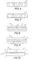
- Figure 6 shows the first partial image I0 provided by the sensor at time t0 and the figure 7 the second the partial image I1 supplied by the sensor at the following time t1, fingerprint 52.
- the images I0, I1, I2, Across In, are transmitted to the inputs of processing 53 of the microprocessor 60 and stored in the RAM 61.
- the algorithm located in the read-only memory 63 performs processing of the images stored in the RAM 61 consisting in trying successively all possible overlaps between images I0 and I1 and assign a correlation coefficient to each test. The best correlation coefficient, will indicate to the system the overlapping position optimum of the two images I0 and I1 and the operation will be repeated with the following image I2 supplied by the sensor 50 to the microprocessor 60 and thus immediately until the complete reconstitution of the fingerprint.
- a strategy correlation is to compare the levels of all elements sensitive of each of the first two successive images I0 and I1 for each case of overlapping of two images possible.
- Figure 8 shows a first test carried out by the algorithm of processing of the system in a first position P1 of superposition of two images I0 and I1, on a zone Z0 common to the two images.
- the processing system compares the levels of sensitive elements of each image I0 and I1 located at the same points in the common area Z0 and if the number of sensitive elements including substantially identical levels is less than a predetermined value, the system changes the position of superimposition of the two images towards a next position P2 (represented in FIG. 9) corresponding to a new superposition zone Z1 of the images I0 and I1 and the system performs a new comparison of the levels of the sensitive elements of the two images I0 and I1 in the zone Z1 and so on for the following positions P3, ....
- a resulting image Ir1, shown in Figure 10, of the two images I0 and I1 could be an image resulting from a weighting between the two images I0 and I1 in their optimum overlapping position Pn, to improve the quality of the resulting overlay image.
- the image Ir1 is kept in the RAM of the microprocessor for the following treatment.
- the system processing algorithm can take into account previous results to a new search for optimal overlap between two successive images to predict what will be the position of most likely overlap for the next image by the fact that the probability that the relative movement of the finger relative to the sensor is substantially constant is very high. This significantly accelerates the speed processing and reconstruction of the complete Irn image of the imprint digital avoiding unnecessary calculations.
- the width of the sensor can be less than the width of the finger, thus further reducing its surface, it will suffice scan the entire fingerprint with adequate speed, the system performing the reconstruction of the complete image.
Description
- le brevet US,4,353,056, décrit un principe de lecture basé sur la variation de la capacité des éléments sensibles du capteur.
- la figure 1 représente un vue générale du capteur d'empreinte ;
- la figure 2 montre l'utilisation du capteur d'empreinte ;
- la figure 3 représente une coupe schématique montrant la constitution du capteur ;
- la figure 4 représente le synoptique d'un exemple de réalisation d'un système de lecture d'empreintes digitales selon l'invention ;
- la figure 5 représente différentes positions relatives du capteur du doigt au moment de la lecture de l'empreinte ;
- les figures 6 et 7 représentent deux images consécutives en sortie du capteur ;
- les figures 8, 9 et 10 représentent des essais de superpositions de deux images successives en sortie du capteur ;
- les figures 11 et 12 représentent deux étapes de reconstitution de l'image complète de l'empreinte digitale.
- de la taille des éléments sensibles du capteur (pixels)
- de la vitesse relative du doigt par rapport au capteur
- du nombre d'images par seconde que pourra délivrer le capteur car il faut impérativement un recouvrement suffisant entre deux images successives
- de l'efficacité de l'algorithme de traitement des images partielles issues du capteur, permettant la reconstitution de l'image complète de l'empreinte.
Claims (18)
- Système de lecture d'une empreinte digitale caractérisé en ce qu'il comporte des moyens de lecture de l'empreinte digitale lorsque le doigt (11,53) et un capteur (10,50) appartenant aux moyens de lecture sont en contact et dans un mouvement relatif de glissement du capteur (10,50) et du doigt (11,53) l'un par rapport à l'autre et des moyens pour reconstituer une image de l'empreinte (52) par superposition d'images partielles (I0,I1,I2,....In) successives obtenues pendant ce mouvement, la surface du capteur étant plus petite que la surface de l'empreinte digitale de manière que le capteur ne délivre que des images partielles de l'empreinte digitale complète.
- Système de lecture d'empreinte digitale selon la revendication 1, caractérisé en ce que le capteur (10,50) est fixé sur un bâti, le mouvement relatif du doigt (11,53) par rapport au capteur étant effectué par glissement du doigt sur le capteur.
- Système de lecture d'empreinte digitale selon la revendication 1, caractérisé en ce que des moyens sont prévus pour déplacer le capteur par rapport à une surface sur laquelle peut être posé un doigt, le mouvement relatif du doigt par rapport au capteur résultant du glissement du capteur par rapport au doigt.
- Système de lecture d'empreinte digitale selon l'une quelconque des revendications 1 à 3, caractérisé en ce que le capteur (10,50) est un circuit intégré comportant une matrice d'éléments sensibles intégrés sur un substrat (20) semi-conducteur dans lequel est intégré un multiplexeur permettant de mesurer individuellement un signal engendré dans la couche active du capteur lors du déplacement relatif du doigt et du capteur, l'un par rapport à l'autre.
- Système de lecture d'empreinte digitale selon l'une quelconque des revendications 1 à 5, caractérisé en ce que le capteur comporte une couche active (30) sensible à la pression et/ou à la température.
- Système de lecture d'empreinte digitale selon la revendication 5, caractérisé en ce que la couche active (30) du circuit intégré est une couche pyro/piézo-électrique permettant de capter un motif matriciel de pression et/ou de température créé par l'empreinte digitale.
- Système de lecture d'empreinte digitale selon l'une quelconque des revendications 1 à 4, caractérisé en ce que les éléments sensibles du capteur sont constitués par des éléments capacitifs permettant de capter le motif matriciel de capacité créé par les sillons du doigt.
- Système de lecture d'empreinte digitale selon l'une quelconque des revendications 4 à 7, caractérisé en ce que l'élément sensible du capteur est de forme rectangulaire.
- Système de lecture d'empreinte digitale selon l'une quelconque des revendications 1 à 8, caractérisé par le fait que la surface du Capteur est plus petite que la surface de l'empreinte digitale et ne délivre que des images partielles de l'empreinte digitale complète.
- Système de lecture d'empreinte digitale selon l'une quelconque des revendications 1 à 9, caractérisé en ce que le capteur se présente sous forme d'une barrette de longueur beaucoup plus petite que sa largeur.
- Système de lecture d'empreinte digitale selon la revendication 10, caractérisé en ce que la largeur de la barrette est sensiblement égale à celle d'un doigt.
- Système de lecture d'empreinte digitale selon l'une des revendications 10 et 11, caractérisé en ce que le capteur a une surface active dont la largeur est comprise entre environ 1cm et 2,5 centimètres et sa longueur inférieure à 5 millimètres.
- Système de lecture d'empreinte digitale selon l'une quelconque des revendications 1 à 12, caractérisé en ce que le capteur comporte une seule ligne d'éléments sensibles.
- Système de lecture d'empreinte digitale selon l'un quelconque des revendications 1 à 13, caractérisé en ce qu'il comporte, pour la reconstruction d'une image d'empreinte (52), un circuit électronique avec un microprocesseur (60), une mémoire morte (63) programmée avec un algorithme permettant de reconstruire l'image complète de l'empreinte et l'identification de la personne et une mémoire vive (61).
- Système de lecture d'empreinte selon l'une des revendications 1 à 14, caractérisé en ce qu'il comporte des moyens de traitement d'images partielles fournies par le capteur, permettant notamment de fournir des contours de lignes de crête d'empreintes digitales, les moyens de reconstitution d'image établissant à partir de ces contours une image globale d'empreinte sous forme de contours.
- Système de lecture d'empreinte digitale selon la revendication 15, caractérisé en ce que les moyens de traitement d'images partielles tiennent compte des résultats précédents à une nouvelle recherche de superposition optimale entre deux images successives pour prédire quelle sera la position de recouvrement la plus probable pour l'image suivante par le fait que la probabilité que le déplacement relatif du doigt par rapport au capteur soit sensiblement constant, est très élevée.
- Système de lecture d'empreinte digitale selon l'une des revendications 1 à 8, caractérisé en ce que le capteur (10,50) comporte une surface active et une matrice de plusieurs lignes d'éléments sensibles pour générer une série d'images (I0,I1,I2,....In), successives partielles se recouvrant, du doigt (11, 53) placé en contact avec cette surface active lors du mouvement relatif de glissement du capteur et du doigt en contact entre la surface active et le doigt, cette surface active étant plus petite que la surface de l'empreinte digitale (52) à lire, les moyens de reconstruction comportant des moyens de corrélation des images partielles successives de recouvrement.
- Procédé de lecture d'une empreinte digitale consistant à,obtenir une série d'images partielles de l'empreinte digitale (52) lors d'un mouvement relatif de glissement du capteur (50) et du doigt (53) en contact, le doigt étant placé en contact direct avec une surface active du capteur, le capteur ayant une surface active plus petite que la surface de l'empreinte digitale à lire, la surface active ayant plusieurs lignes d'éléments sensibles, chaque image partielle recouvrant l'image partielle précédente etreconstruire une image globale par corrélation des images partielles se recouvrant.
Applications Claiming Priority (2)
| Application Number | Priority Date | Filing Date | Title |
|---|---|---|---|
| FR9607419 | 1996-06-14 | ||
| FR9607419A FR2749955B1 (fr) | 1996-06-14 | 1996-06-14 | Systeme de lecture d'empreintes digitales |
Publications (2)
| Publication Number | Publication Date |
|---|---|
| EP0813164A1 EP0813164A1 (fr) | 1997-12-17 |
| EP0813164B1 true EP0813164B1 (fr) | 2003-03-26 |
Family
ID=9493060
Family Applications (1)
| Application Number | Title | Priority Date | Filing Date |
|---|---|---|---|
| EP97401345A Expired - Lifetime EP0813164B1 (fr) | 1996-06-14 | 1997-06-13 | Système et Procédé de lecture d'empreintes digitales |
Country Status (16)
| Country | Link |
|---|---|
| US (2) | US6289114B1 (fr) |
| EP (1) | EP0813164B1 (fr) |
| JP (1) | JP4408965B2 (fr) |
| KR (1) | KR100694549B1 (fr) |
| CN (1) | CN1119766C (fr) |
| AR (1) | AR007564A1 (fr) |
| AT (1) | ATE235718T1 (fr) |
| BR (1) | BR9703596A (fr) |
| CA (1) | CA2206825C (fr) |
| CO (1) | CO5160332A1 (fr) |
| DE (1) | DE69720109T2 (fr) |
| ES (1) | ES2191816T3 (fr) |
| FR (1) | FR2749955B1 (fr) |
| IL (1) | IL121045A (fr) |
| MX (1) | MX9704379A (fr) |
| ZA (1) | ZA975193B (fr) |
Cited By (2)
| Publication number | Priority date | Publication date | Assignee | Title |
|---|---|---|---|---|
| US7082214B2 (en) | 2003-11-10 | 2006-07-25 | Fujitsu Limited | Authentication device, authentication system, and sensor |
| US8903142B2 (en) | 2010-07-12 | 2014-12-02 | Fingerprint Cards Ab | Biometric verification device and method |
Families Citing this family (346)
| Publication number | Priority date | Publication date | Assignee | Title |
|---|---|---|---|---|
| NO304766B1 (no) * | 1997-06-16 | 1999-02-08 | Sintef | Fingeravtrykksensor |
| US6330345B1 (en) | 1997-11-17 | 2001-12-11 | Veridicom, Inc. | Automatic adjustment processing for sensor devices |
| TW399186B (en) * | 1997-12-10 | 2000-07-21 | Canon Kk | Image processing apparatus and image processing method |
| US6317508B1 (en) * | 1998-01-13 | 2001-11-13 | Stmicroelectronics, Inc. | Scanning capacitive semiconductor fingerprint detector |
| US6408087B1 (en) | 1998-01-13 | 2002-06-18 | Stmicroelectronics, Inc. | Capacitive semiconductor user input device |
| FR2773898B1 (fr) | 1998-01-16 | 2003-03-28 | Richard V Rault | Dispositif d'authentification de personne par ses empreintes digitales |
| NO307065B1 (no) * | 1998-02-26 | 2000-01-31 | Idex As | Fingeravtrykksensor |
| US6178255B1 (en) * | 1998-04-28 | 2001-01-23 | Cross Match Technologies, Inc. | Individualized fingerprint scanner |
| IL127569A0 (en) | 1998-09-16 | 1999-10-28 | Comsense Technologies Ltd | Interactive toys |
| US6607136B1 (en) | 1998-09-16 | 2003-08-19 | Beepcard Inc. | Physical presence digital authentication system |
| JP2002527012A (ja) * | 1998-10-02 | 2002-08-20 | コムセンス・テクノロジーズ・リミテッド | コンピュータとの相互作用のためのカード |
| EP1121053B1 (fr) | 1998-10-12 | 2005-04-13 | STMicroelectronics N.V. | Enceinte de protection pour un dispositif de detection d'empreintes digitales |
| JP3150126B2 (ja) * | 1999-02-03 | 2001-03-26 | 静岡日本電気株式会社 | 指紋入力装置 |
| ATE285710T1 (de) * | 1999-02-12 | 2005-01-15 | Precise Biometrics Ab | System und verfahren zur überprüfung von fingerabdrücken |
| US6097035A (en) * | 1999-02-22 | 2000-08-01 | Digital Persona, Inc. | Fingerprint detection apparatus with partial fingerprint images |
| US6674993B1 (en) * | 1999-04-30 | 2004-01-06 | Microvision, Inc. | Method and system for identifying data locations associated with real world observations |
| US6795569B1 (en) | 1999-05-11 | 2004-09-21 | Authentec, Inc. | Fingerprint image compositing method and associated apparatus |
| EP1054340B1 (fr) * | 1999-05-17 | 2008-05-28 | Nippon Telegraph and Telephone Corporation | Appareil et méthode de reconnaissance des modèles de surface |
| EP1207786B1 (fr) * | 1999-08-09 | 2009-10-07 | Sonavation, Inc. | Lecteur d'empreintes digitales comportant un film piezo-electrique |
| US8019609B2 (en) | 1999-10-04 | 2011-09-13 | Dialware Inc. | Sonic/ultrasonic authentication method |
| GB2357335B (en) * | 1999-12-17 | 2004-04-07 | Nokia Mobile Phones Ltd | Fingerprint recognition and pointing device |
| US6950540B2 (en) * | 2000-01-31 | 2005-09-27 | Nec Corporation | Fingerprint apparatus and method |
| JP2006053768A (ja) * | 2004-08-12 | 2006-02-23 | Nec Corp | 指紋装置および指紋法 |
| KR100887275B1 (ko) * | 2000-03-23 | 2009-03-06 | 크로스 매치 테크놀로지스, 인크. | 압전 식별 디바이스 및 그 응용 |
| US7067962B2 (en) | 2000-03-23 | 2006-06-27 | Cross Match Technologies, Inc. | Multiplexer for a piezo ceramic identification device |
| US20030001459A1 (en) * | 2000-03-23 | 2003-01-02 | Cross Match Technologies, Inc. | Secure wireless sales transaction using print information to verify a purchaser's identity |
| US7132780B2 (en) * | 2000-03-23 | 2006-11-07 | Cross Match Technologies, Inc. | Method for obtaining biometric data for an individual in a secure transaction |
| US6643389B1 (en) * | 2000-03-28 | 2003-11-04 | Stmicroelectronics, Inc. | Narrow array capacitive fingerprint imager |
| JP4426733B2 (ja) * | 2000-03-31 | 2010-03-03 | 富士通株式会社 | 指紋データ合成方法,指紋データ合成装置,指紋データ合成プログラムおよび同プログラムを記録したコンピュータ読取可能な記録媒体 |
| WO2001080167A1 (fr) * | 2000-04-13 | 2001-10-25 | Nanyang Technological University | Procede et dispositif destines a determiner un gabarit presentant toutes les particularites a partir de plusieurs gabarits presentant seulement certaines particularites |
| SE0001761L (sv) * | 2000-05-15 | 2001-07-02 | Ericsson Telefon Ab L M | Metod för alstring av en sammansatt bild samt en apparat för detektering av fingeravtryck |
| NO315017B1 (no) * | 2000-06-09 | 2003-06-23 | Idex Asa | Sensorbrikke, s¶rlig for måling av strukturer i en fingeroverflate |
| US7565541B1 (en) * | 2000-06-21 | 2009-07-21 | Microvision, Inc. | Digital fingerprint identification system |
| FR2811162B1 (fr) * | 2000-06-29 | 2006-08-18 | Somfy | Dispositif de commande d'un moteur a deux sens de rotation |
| US6898301B2 (en) * | 2000-07-10 | 2005-05-24 | Casio Computer Co., Ltd. | Authentication system based on fingerprint and electronic device employed for the system |
| SE516860C2 (sv) * | 2000-07-17 | 2002-03-12 | Precise Biometrics Ab | Anordning och förfarande för fingeravtryckskontroll, genom kontroll av särdrag i delbilder |
| JP4897470B2 (ja) * | 2000-07-24 | 2012-03-14 | 株式会社ディー・ディー・エス | 指紋照合装置及び指紋照合プログラム |
| JP4221220B2 (ja) * | 2000-07-24 | 2009-02-12 | 株式会社ディー・ディー・エス | 指紋照合装置、指紋照合方法及び指紋照合プログラム |
| JP3780830B2 (ja) * | 2000-07-28 | 2006-05-31 | 日本電気株式会社 | 指紋識別方法及び装置 |
| US7289649B1 (en) * | 2000-08-10 | 2007-10-30 | Avago Technologies Ecbu Ip (Singapore) Pte. Ltd. | Fingerprint imager |
| EP1374146B1 (fr) * | 2000-12-05 | 2005-10-19 | Validity Sensors Inc. | Systemes de detection d'empreinte digitale capacitifs a ouverture de glissement et procedes associes |
| DE10109560B4 (de) * | 2001-02-28 | 2007-02-08 | Infineon Technologies Ag | Lesevorrichtung für Fingerabdrücke |
| SE0100887D0 (sv) † | 2001-03-15 | 2001-03-15 | Fingerprint Cards Ab | Anordning och metod för behandling av fingeravtrycksinformation |
| US9219708B2 (en) | 2001-03-22 | 2015-12-22 | DialwareInc. | Method and system for remotely authenticating identification devices |
| AU2002305257A1 (en) | 2001-04-27 | 2002-11-11 | Atrua Technologies, Inc. | Capacitive sensor system with improved capacitance measuring sensitivity |
| TWI241531B (en) * | 2001-05-22 | 2005-10-11 | Atrua Technologies Inc | Improved connection assembly for integrated circuit sensors |
| US7259573B2 (en) * | 2001-05-22 | 2007-08-21 | Atrua Technologies, Inc. | Surface capacitance sensor system using buried stimulus electrode |
| EP1412765A4 (fr) * | 2001-05-22 | 2008-02-06 | Atrua Technologies Inc | Systeme de detection de la capacite de surface utilisant une electrode de stimuli noyee |
| KR100430054B1 (ko) * | 2001-05-25 | 2004-05-03 | 주식회사 씨크롭 | 리니어 지문 검출센서를 이용한 지문획득 방법 |
| US7043061B2 (en) * | 2001-06-27 | 2006-05-09 | Laurence Hamid | Swipe imager with multiple sensing arrays |
| US7203347B2 (en) * | 2001-06-27 | 2007-04-10 | Activcard Ireland Limited | Method and system for extracting an area of interest from within a swipe image of a biological surface |
| US7197168B2 (en) * | 2001-07-12 | 2007-03-27 | Atrua Technologies, Inc. | Method and system for biometric image assembly from multiple partial biometric frame scans |
| US7272248B2 (en) * | 2001-07-16 | 2007-09-18 | Activcard Ireland Limited | Biometric imaging device compensating for non-biometric parameters |
| US6944321B2 (en) | 2001-07-20 | 2005-09-13 | Activcard Ireland Limited | Image distortion compensation technique and apparatus |
| JP2003067751A (ja) * | 2001-08-27 | 2003-03-07 | Dds:Kk | 指紋照合装置、指紋照合方法及び指紋照合プログラム |
| US20030104693A1 (en) * | 2001-11-30 | 2003-06-05 | Siegel Harry M. | Use of fluoropolymer coating for planarizing and passivating integrated circuit devices |
| US6762470B2 (en) | 2001-11-30 | 2004-07-13 | Stmicroelectronics, Inc. | Fingerprint sensor having a portion of the fluorocarbon polymer physical interface layer amorphized |
| US6707093B2 (en) | 2001-11-30 | 2004-03-16 | Stmicroelectronics, Inc. | Selective ionic implantation of fluoropolymer film to modify the sensitivity of underlying sensing capacitors |
| JP3902473B2 (ja) * | 2002-01-17 | 2007-04-04 | 富士通株式会社 | 生体情報を用いた本人認証方法 |
| US7039223B2 (en) * | 2002-02-14 | 2006-05-02 | Wong Jacob Y | Authentication method utilizing a sequence of linear partial fingerprint signatures selected by a personal code |
| DE60314989T2 (de) * | 2002-02-18 | 2008-04-03 | Precise Biometrics Ab | Verfahren und Einrichtung zur Überprüfung von Fingerabdrücken |
| JP2003242489A (ja) * | 2002-02-20 | 2003-08-29 | Canon Inc | 画像入力装置及び指紋認識装置 |
| JP3766034B2 (ja) * | 2002-02-20 | 2006-04-12 | 富士通株式会社 | 指紋センサ装置及びその製造方法 |
| CN1235172C (zh) * | 2002-02-20 | 2006-01-04 | 佳能株式会社 | 图像输入装置 |
| JP4027118B2 (ja) * | 2002-02-25 | 2007-12-26 | 富士通株式会社 | 本人認証方法、プログラム及び装置 |
| JP4169185B2 (ja) * | 2002-02-25 | 2008-10-22 | 富士通株式会社 | 画像連結方法、プログラム及び装置 |
| US7035443B2 (en) * | 2002-03-22 | 2006-04-25 | Wong Jacob Y | Personal choice biometric signature |
| JP4022861B2 (ja) * | 2002-04-10 | 2007-12-19 | 日本電気株式会社 | 指紋認証システム、指紋認証方法及び指紋認証プログラム |
| US7171784B2 (en) * | 2002-04-12 | 2007-02-06 | Newell Operating Company | Tilt-latch for a sash window |
| US20040042641A1 (en) * | 2002-08-30 | 2004-03-04 | Jakubowski Peter Joel | Personnel identity verification system |
| CN100364480C (zh) * | 2002-09-17 | 2008-01-30 | 富士通株式会社 | 生物特征信息获取设备和使用生物特征信息的认证设备 |
| JP2004110438A (ja) * | 2002-09-18 | 2004-04-08 | Nec Corp | 画像処理装置、画像処理方法及びプログラム |
| JP4262471B2 (ja) * | 2002-11-12 | 2009-05-13 | 富士通株式会社 | 生体特徴データ取得装置 |
| DE10254614B4 (de) * | 2002-11-22 | 2006-04-20 | Infineon Technologies Ag | Verfahren zur Detektion einer Relativbewegung eines Fingers gegenüber einer Sensorfläche |
| US20040101172A1 (en) * | 2002-11-26 | 2004-05-27 | Stmicroelectronics, Inc. | Imaging system with locator bar for accurate fingerprint recognition |
| FR2850190B1 (fr) * | 2003-01-21 | 2006-04-28 | Atmel Grenoble Sa | Procede et dispositif de reconnaissance de personne |
| FI115109B (fi) * | 2003-01-22 | 2005-02-28 | Nokia Corp | Tunnistusjärjestely ja tunnistusjärjestelyn käsittävä matkaviestin |
| FI20030102A0 (fi) * | 2003-01-22 | 2003-01-22 | Nokia Corp | Henkilön varmennusjärjestely |
| JP3770241B2 (ja) * | 2003-03-04 | 2006-04-26 | 株式会社日立製作所 | 個人認証装置及び個人認証方法 |
| US20040234105A1 (en) * | 2003-05-19 | 2004-11-25 | Quen-Zong Wu | Method of automatic vehicle licence plate recognition by color discrimination and reorganization |
| US6923370B2 (en) * | 2003-05-20 | 2005-08-02 | Bradley L. Gotfried | Access system |
| US7200250B2 (en) * | 2003-05-20 | 2007-04-03 | Lightuning Tech, Inc. | Sweep-type fingerprint sensor module |
| US20040232228A1 (en) * | 2003-05-20 | 2004-11-25 | Gotfried Bradley L. | Monitoring system |
| US6888445B2 (en) * | 2003-05-20 | 2005-05-03 | Bradley L. Gotfried | Vehicle identification system |
| JP3733357B2 (ja) * | 2003-05-28 | 2006-01-11 | キヤノン株式会社 | 指紋入力装置及びこれを用いた個人認証システム |
| US7474772B2 (en) | 2003-06-25 | 2009-01-06 | Atrua Technologies, Inc. | System and method for a miniature user input device |
| JP3891572B2 (ja) * | 2003-06-30 | 2007-03-14 | キヤノン株式会社 | 指紋入力装置、個人認証システムおよび電子機器 |
| KR100613697B1 (ko) * | 2003-07-18 | 2006-08-21 | 학교법인연세대학교 | 손가락의 슬라이딩/롤링에 따른 지문영상획득방법 |
| FR2857768B1 (fr) * | 2003-07-18 | 2006-01-06 | Atmel Grenoble Sa | Procede d'acquisition d'image d'empreinte digitale |
| US7587072B2 (en) * | 2003-08-22 | 2009-09-08 | Authentec, Inc. | System for and method of generating rotational inputs |
| DE10339743B4 (de) * | 2003-08-28 | 2007-08-02 | Infineon Technologies Ag | Verfahren zum Vergleich eines Testfingerabdrucks mit einem gespeicherten Referenzfingerabdruck und zur Durchführung des Verfahrens geeignete Vorrichtung |
| US7351974B2 (en) * | 2003-09-05 | 2008-04-01 | Authentec, Inc. | Integrated circuit infrared sensor and associated methods |
| CN1875370B (zh) * | 2003-09-05 | 2010-04-14 | 奥森泰克公司 | 利用具有不同选择性的生物测量学的多生物测量手指传感器以及相关方法 |
| CN100547602C (zh) * | 2003-09-11 | 2009-10-07 | Nxp股份有限公司 | 利用具有光电子速度传感器的扫描型成像器的指纹检测方法 |
| EP1678655B1 (fr) * | 2003-09-24 | 2008-11-12 | Authentec, Inc. | Capteur biometriques d'empreintes digitales pourvu d'un systeme electronique reparti sur un film mince et des substrats monocristallin et procedes correspondants |
| US7787667B2 (en) * | 2003-10-01 | 2010-08-31 | Authentec, Inc. | Spot-based finger biometric processing method and associated sensor |
| WO2005034021A1 (fr) * | 2003-10-01 | 2005-04-14 | Authentec, Inc. | Procede de traitement biometrique de doigt et capteurs biometriques de doigt associes |
| US7599530B2 (en) * | 2003-10-01 | 2009-10-06 | Authentec, Inc. | Methods for matching ridge orientation characteristic maps and associated finger biometric sensor |
| JP3924558B2 (ja) * | 2003-11-17 | 2007-06-06 | 富士通株式会社 | 生体情報採取装置 |
| FR2862394B1 (fr) * | 2003-11-18 | 2006-02-17 | Atmel Grenoble Sa | Generateur de sequences binaires aleatoires |
| JP2005173700A (ja) * | 2003-12-08 | 2005-06-30 | Canon Inc | 指紋読み取り装置及び個人認証システム |
| DE10358738B3 (de) * | 2003-12-11 | 2005-06-02 | Smiths Heimann Biometrics Gmbh | Verfahren und Anordnung zur elektronischen Aufnahme abgerollter Fingerabdrücke |
| JP4468896B2 (ja) * | 2004-01-13 | 2010-05-26 | 富士通株式会社 | 生体情報による認証装置 |
| US7697729B2 (en) * | 2004-01-29 | 2010-04-13 | Authentec, Inc. | System for and method of finger initiated actions |
| JP4454335B2 (ja) * | 2004-02-12 | 2010-04-21 | Necインフロンティア株式会社 | 指紋入力装置 |
| US7356170B2 (en) * | 2004-02-12 | 2008-04-08 | Lenovo (Singapore) Pte. Ltd. | Fingerprint matching method and system |
| JP3996133B2 (ja) * | 2004-02-16 | 2007-10-24 | シャープ株式会社 | 画像照合装置、画像照合方法、画像照合プログラム、および画像照合プログラムを記録したコンピュータ読取可能な記録媒体 |
| JP4462988B2 (ja) * | 2004-04-13 | 2010-05-12 | Necインフロンティア株式会社 | 指紋読取方法および指紋読取システム |
| US8447077B2 (en) * | 2006-09-11 | 2013-05-21 | Validity Sensors, Inc. | Method and apparatus for fingerprint motion tracking using an in-line array |
| US8175345B2 (en) | 2004-04-16 | 2012-05-08 | Validity Sensors, Inc. | Unitized ergonomic two-dimensional fingerprint motion tracking device and method |
| US8358815B2 (en) | 2004-04-16 | 2013-01-22 | Validity Sensors, Inc. | Method and apparatus for two-dimensional finger motion tracking and control |
| US8229184B2 (en) | 2004-04-16 | 2012-07-24 | Validity Sensors, Inc. | Method and algorithm for accurate finger motion tracking |
| US8165355B2 (en) | 2006-09-11 | 2012-04-24 | Validity Sensors, Inc. | Method and apparatus for fingerprint motion tracking using an in-line array for use in navigation applications |
| US8131026B2 (en) | 2004-04-16 | 2012-03-06 | Validity Sensors, Inc. | Method and apparatus for fingerprint image reconstruction |
| WO2005104012A1 (fr) * | 2004-04-16 | 2005-11-03 | Validity Sensors, Inc. | Procede et dispositif de detection de la position d'un doigt |
| WO2005106774A2 (fr) * | 2004-04-23 | 2005-11-10 | Validity Sensors, Inc. | Procedes et appareil permettant l'acquisition d'une image d'empreinte digitale par glissement |
| US7542590B1 (en) | 2004-05-07 | 2009-06-02 | Yt Acquisition Corporation | System and method for upgrading biometric data |
| US8229185B2 (en) | 2004-06-01 | 2012-07-24 | Lumidigm, Inc. | Hygienic biometric sensors |
| CN1332297C (zh) * | 2004-06-09 | 2007-08-15 | 夏普株式会社 | 可进行定点操作的传感器表面的保护外罩 |
| JP4411150B2 (ja) * | 2004-06-30 | 2010-02-10 | Necインフロンティア株式会社 | 画像構成方法、指紋画像構成装置およびプログラム |
| JP4411152B2 (ja) * | 2004-07-05 | 2010-02-10 | Necインフロンティア株式会社 | 指紋読取方法、指紋読取システム及びプログラム |
| US20060204061A1 (en) * | 2004-07-16 | 2006-09-14 | Atmel Grenoble S.A. | Method for the acquisition of an image of a finger print |
| WO2006009319A1 (fr) * | 2004-07-22 | 2006-01-26 | Nec Corporation | Système de traitement d’images |
| JP4339221B2 (ja) * | 2004-09-30 | 2009-10-07 | Necインフロンティア株式会社 | 画像構成方法、指紋画像構成装置およびプログラム |
| DE602005022900D1 (de) | 2004-10-04 | 2010-09-23 | Validity Sensors Inc | Fingerabdruckerfassende konstruktionen mit einem substrat |
| JP2006107366A (ja) * | 2004-10-08 | 2006-04-20 | Fujitsu Ltd | 生体情報入力装置,生体認証装置,生体情報処理方法,生体情報処理プログラムおよび同プログラムを記録したコンピュータ読取可能な記録媒体 |
| US7280679B2 (en) * | 2004-10-08 | 2007-10-09 | Atrua Technologies, Inc. | System for and method of determining pressure on a finger sensor |
| WO2006044815A1 (fr) * | 2004-10-13 | 2006-04-27 | Authentec, Inc. | Dispositif de detection digitale destine a une navigation et methodes associees |
| US20060093192A1 (en) | 2004-11-03 | 2006-05-04 | Bechtel J S | Finger guide device |
| DE102004053900A1 (de) * | 2004-11-05 | 2006-05-11 | Tbs Holding Ag | Verfahren und Vorrichtung für das Erfassen von biometrischen Daten |
| TW200632764A (en) | 2004-11-15 | 2006-09-16 | Nec Corp | Biological feature input device |
| FR2878632B1 (fr) * | 2004-12-01 | 2007-02-09 | Sagem | Procede d'identification d'un individu a partir de fragments d'image |
| JP2006221514A (ja) * | 2005-02-14 | 2006-08-24 | Canon Inc | 生体認証装置及び画像取得方法 |
| US20060181521A1 (en) * | 2005-02-14 | 2006-08-17 | Atrua Technologies, Inc. | Systems for dynamically illuminating touch sensors |
| WO2007024259A2 (fr) * | 2005-02-17 | 2007-03-01 | Authentec, Inc. | Appareil a capteur de doigt utilisant le reechantillonnage des images et procedes correspondants |
| US7831070B1 (en) | 2005-02-18 | 2010-11-09 | Authentec, Inc. | Dynamic finger detection mechanism for a fingerprint sensor |
| TWI303388B (en) * | 2005-03-18 | 2008-11-21 | Egis Technology Inc | A sweep-type image sensing chip with image matching function and processing method therefor |
| WO2006114891A1 (fr) * | 2005-04-25 | 2006-11-02 | Fujitsu Limited | Procede de gestion de fichiers |
| TWI267791B (en) * | 2005-05-13 | 2006-12-01 | Lite On Semiconductor Corp | Handheld device for acquiring fingerprint information |
| CN100373393C (zh) * | 2005-06-30 | 2008-03-05 | 中国科学院自动化研究所 | 基于运动估计的扫描指纹图像重构方法 |
| US7460697B2 (en) * | 2005-07-19 | 2008-12-02 | Validity Sensors, Inc. | Electronic fingerprint sensor with differential noise cancellation |
| TWI297464B (en) * | 2005-07-21 | 2008-06-01 | Lightuning Tech Inc | Wireless peripheral device having a sweep-type fingerprint sensing chip |
| US7790406B2 (en) * | 2005-08-11 | 2010-09-07 | Sru Biosystems, Inc | Grating-based sensor combining label-free binding detection and fluorescence amplification and readout system for sensor |
| KR101006793B1 (ko) * | 2005-08-11 | 2011-01-10 | 에스알유 바이오시스템즈, 인코포레이티드 | 라벨 없는 바인딩 검출 및 형광 증폭과 조합된 격자-기반센서 및 센서를 위한 판독 시스템 |
| US8358816B2 (en) | 2005-10-18 | 2013-01-22 | Authentec, Inc. | Thinned finger sensor and associated methods |
| WO2007047823A1 (fr) * | 2005-10-18 | 2007-04-26 | Authentec, Inc. | Capteur d'empreinte digitale presentant un montage perfectionne, et methodes associees |
| US7555344B2 (en) * | 2005-10-28 | 2009-06-30 | Cyberonics, Inc. | Selective neurostimulation for treating epilepsy |
| US7809211B2 (en) | 2005-11-17 | 2010-10-05 | Upek, Inc. | Image normalization for computed image construction |
| JP4740743B2 (ja) * | 2006-01-06 | 2011-08-03 | 富士通株式会社 | 生体情報入力装置 |
| JP4547629B2 (ja) * | 2006-02-10 | 2010-09-22 | ソニー株式会社 | 登録装置、登録方法及び登録プログラム |
| US7849312B2 (en) * | 2006-03-24 | 2010-12-07 | Atmel Corporation | Method and system for secure external TPM password generation and use |
| US20070237366A1 (en) * | 2006-03-24 | 2007-10-11 | Atmel Corporation | Secure biometric processing system and method of use |
| JP4757071B2 (ja) | 2006-03-27 | 2011-08-24 | 富士通株式会社 | 指紋認証装置および情報処理装置 |
| NZ571961A (en) * | 2006-03-27 | 2011-10-28 | Fabrizio Borracci | A method for making a secure personal card and its working process |
| JP4182987B2 (ja) | 2006-04-28 | 2008-11-19 | 日本電気株式会社 | 画像読取装置 |
| US7545621B2 (en) * | 2006-07-24 | 2009-06-09 | Yt Acquisition Corporation | Electrostatic discharge structure for a biometric sensor |
| US20080049987A1 (en) * | 2006-08-28 | 2008-02-28 | Champagne Katrina S | Fingerprint recognition system |
| JP4910644B2 (ja) * | 2006-11-02 | 2012-04-04 | ソニー株式会社 | 撮像装置 |
| KR101035930B1 (ko) | 2007-01-24 | 2011-05-23 | 후지쯔 가부시끼가이샤 | 화상 판독 장치, 화상 판독 프로그램을 기록한 기록 매체, 화상 판독 방법 |
| US7385381B1 (en) | 2007-03-06 | 2008-06-10 | Atmel Switzerland | Sensor manufacture with data storage |
| US20080219520A1 (en) * | 2007-03-06 | 2008-09-11 | Atmel Corporation | Sensor monitoring |
| US20080226135A1 (en) * | 2007-03-12 | 2008-09-18 | Atmel Corporation | Incremental recognition |
| US8107212B2 (en) | 2007-04-30 | 2012-01-31 | Validity Sensors, Inc. | Apparatus and method for protecting fingerprint sensing circuitry from electrostatic discharge |
| US8290150B2 (en) | 2007-05-11 | 2012-10-16 | Validity Sensors, Inc. | Method and system for electronically securing an electronic device using physically unclonable functions |
| JP4389971B2 (ja) | 2007-06-19 | 2009-12-24 | ミツミ電機株式会社 | 指紋画像形成装置及びこれに用いる指移動量推定方法 |
| US8050467B2 (en) * | 2007-09-19 | 2011-11-01 | Chipbond Technology Corporation | Package, packaging method and substrate thereof for sliding type thin fingerprint sensor |
| CN101809581B (zh) | 2007-09-24 | 2014-12-10 | 苹果公司 | 电子设备中的嵌入式验证系统 |
| JP4883185B2 (ja) | 2007-11-09 | 2012-02-22 | 富士通株式会社 | 生体情報読取装置,生体情報読取方法,及び生体情報読取プログラム |
| JP2009134562A (ja) * | 2007-11-30 | 2009-06-18 | Oki Semiconductor Co Ltd | 画像処理装置 |
| KR100905642B1 (ko) | 2007-12-13 | 2009-06-30 | 삼성전기주식회사 | 칩 내장형 인쇄회로기판 및 그 제조방법 |
| US8204281B2 (en) | 2007-12-14 | 2012-06-19 | Validity Sensors, Inc. | System and method to remove artifacts from fingerprint sensor scans |
| US20090155456A1 (en) * | 2007-12-14 | 2009-06-18 | Validity Sensors, Inc. | System and Method for Fingerprint-Resistant Surfaces for Devices Using Fingerprint Sensors |
| US8276816B2 (en) | 2007-12-14 | 2012-10-02 | Validity Sensors, Inc. | Smart card system with ergonomic fingerprint sensor and method of using |
| US8600120B2 (en) | 2008-01-03 | 2013-12-03 | Apple Inc. | Personal computing device control using face detection and recognition |
| US20090175539A1 (en) * | 2008-01-09 | 2009-07-09 | Authorizer Technologies, Inc. | Method and system for swipe sensor image alignment using fourier phase analysis |
| US11272874B2 (en) * | 2008-01-25 | 2022-03-15 | Flint Hills Scientific, Llc | Contingent cardio-protection for epilepsy patients |
| US8005276B2 (en) | 2008-04-04 | 2011-08-23 | Validity Sensors, Inc. | Apparatus and method for reducing parasitic capacitive coupling and noise in fingerprint sensing circuits |
| US8116540B2 (en) | 2008-04-04 | 2012-02-14 | Validity Sensors, Inc. | Apparatus and method for reducing noise in fingerprint sensing circuits |
| US8358803B2 (en) * | 2008-05-05 | 2013-01-22 | Sonavation, Inc. | Navigation using fourier phase technique |
| US8634604B2 (en) * | 2008-05-05 | 2014-01-21 | Sonavation, Inc. | Method and system for enhanced image alignment |
| US8421483B2 (en) * | 2008-06-13 | 2013-04-16 | Sony Ericsson Mobile Communications Ab | Touch and force sensing for input devices |
| JP5040835B2 (ja) * | 2008-07-04 | 2012-10-03 | 富士通株式会社 | 生体情報読取装置、生体情報読取方法および生体情報読取プログラム |
| EP2321764A4 (fr) | 2008-07-22 | 2012-10-10 | Validity Sensors Inc | Système, dispositif et procédé de fixation d'un composant de dispositif |
| JP5206218B2 (ja) | 2008-08-20 | 2013-06-12 | 富士通株式会社 | 指紋画像取得装置、指紋認証装置、指紋画像取得方法及び指紋認証方法 |
| NO20083766L (no) * | 2008-09-01 | 2010-03-02 | Idex Asa | Overflatesensor |
| US8391568B2 (en) | 2008-11-10 | 2013-03-05 | Validity Sensors, Inc. | System and method for improved scanning of fingerprint edges |
| US8278946B2 (en) | 2009-01-15 | 2012-10-02 | Validity Sensors, Inc. | Apparatus and method for detecting finger activity on a fingerprint sensor |
| US8600122B2 (en) * | 2009-01-15 | 2013-12-03 | Validity Sensors, Inc. | Apparatus and method for culling substantially redundant data in fingerprint sensing circuits |
| US8374407B2 (en) | 2009-01-28 | 2013-02-12 | Validity Sensors, Inc. | Live finger detection |
| KR101658991B1 (ko) * | 2009-06-19 | 2016-09-22 | 삼성전자주식회사 | 터치 패널 및 이를 구비한 전자 기기 |
| US8432252B2 (en) | 2009-06-19 | 2013-04-30 | Authentec, Inc. | Finger sensor having remote web based notifications |
| KR101667801B1 (ko) * | 2009-06-19 | 2016-10-20 | 삼성전자주식회사 | 터치 패널 및 이를 구비한 전자 기기 |
| US8455961B2 (en) * | 2009-06-19 | 2013-06-04 | Authentec, Inc. | Illuminated finger sensor assembly for providing visual light indications including IC finger sensor grid array package |
| US8618910B2 (en) | 2009-08-07 | 2013-12-31 | Authentec, Inc. | Finger biometric sensor including laterally adjacent piezoelectric transducer layer and associated methods |
| JP5504818B2 (ja) * | 2009-10-23 | 2014-05-28 | ソニー株式会社 | 動作関連演算装置、動作関連演算方法、プログラム、動作関連再生システム |
| US9336428B2 (en) | 2009-10-30 | 2016-05-10 | Synaptics Incorporated | Integrated fingerprint sensor and display |
| US9400911B2 (en) | 2009-10-30 | 2016-07-26 | Synaptics Incorporated | Fingerprint sensor and integratable electronic display |
| US9274553B2 (en) | 2009-10-30 | 2016-03-01 | Synaptics Incorporated | Fingerprint sensor and integratable electronic display |
| US8433110B2 (en) * | 2009-12-11 | 2013-04-30 | Sonavation, Inc. | Pulse-rate detection using a fingerprint sensor |
| NO20093601A1 (no) | 2009-12-29 | 2011-06-30 | Idex Asa | Overflatesensor |
| KR101616875B1 (ko) * | 2010-01-07 | 2016-05-02 | 삼성전자주식회사 | 터치 패널 및 이를 구비한 전자기기 |
| US8866347B2 (en) | 2010-01-15 | 2014-10-21 | Idex Asa | Biometric image sensing |
| US8421890B2 (en) | 2010-01-15 | 2013-04-16 | Picofield Technologies, Inc. | Electronic imager using an impedance sensor grid array and method of making |
| US8791792B2 (en) | 2010-01-15 | 2014-07-29 | Idex Asa | Electronic imager using an impedance sensor grid array mounted on or about a switch and method of making |
| KR101631892B1 (ko) * | 2010-01-28 | 2016-06-21 | 삼성전자주식회사 | 터치 패널 및 이를 구비한 전자기기 |
| WO2011092827A1 (fr) | 2010-01-28 | 2011-08-04 | 富士通株式会社 | Dispositif, procédé et programme de traitement d'informations d'ordre biologique |
| US9666635B2 (en) | 2010-02-19 | 2017-05-30 | Synaptics Incorporated | Fingerprint sensing circuit |
| JP2010140508A (ja) * | 2010-03-01 | 2010-06-24 | Nec Corp | 指紋装置および指紋法 |
| US8716613B2 (en) | 2010-03-02 | 2014-05-06 | Synaptics Incoporated | Apparatus and method for electrostatic discharge protection |
| KR101710523B1 (ko) * | 2010-03-22 | 2017-02-27 | 삼성전자주식회사 | 터치 패널 및 이를 구비한 전자기기 |
| US8833657B2 (en) * | 2010-03-30 | 2014-09-16 | Willie Anthony Johnson | Multi-pass biometric scanner |
| FR2959657B1 (fr) | 2010-05-06 | 2012-06-22 | Commissariat Energie Atomique | Transducteur de variation temporelle de température, puce électronique incorporant ce transducteur et procédé de fabrication de cette puce |
| FR2959814B1 (fr) | 2010-05-06 | 2013-07-05 | Commissariat Energie Atomique | Procédé de calibration d'une puce électronique, puce électronique et détecteur de motif thermique pour ce procédé |
| KR101661728B1 (ko) | 2010-05-11 | 2016-10-04 | 삼성전자주식회사 | 사용자 입력 장치 및 이를 구비한 전자 기기 |
| US9001040B2 (en) | 2010-06-02 | 2015-04-07 | Synaptics Incorporated | Integrated fingerprint sensor and navigation device |
| US8331096B2 (en) | 2010-08-20 | 2012-12-11 | Validity Sensors, Inc. | Fingerprint acquisition expansion card apparatus |
| WO2012031634A1 (fr) * | 2010-09-10 | 2012-03-15 | Sony Ericsson Mobile Communications Ab | Procédé et dispositif |
| KR101809191B1 (ko) * | 2010-10-11 | 2018-01-18 | 삼성전자주식회사 | 터치 패널 |
| KR101735715B1 (ko) | 2010-11-23 | 2017-05-15 | 삼성전자주식회사 | 입력 감지 소자 및 이를 구비한 터치 패널 |
| US8538097B2 (en) | 2011-01-26 | 2013-09-17 | Validity Sensors, Inc. | User input utilizing dual line scanner apparatus and method |
| US8594393B2 (en) * | 2011-01-26 | 2013-11-26 | Validity Sensors | System for and method of image reconstruction with dual line scanner using line counts |
| GB2489100A (en) | 2011-03-16 | 2012-09-19 | Validity Sensors Inc | Wafer-level packaging for a fingerprint sensor |
| KR101784436B1 (ko) | 2011-04-18 | 2017-10-11 | 삼성전자주식회사 | 터치 패널 및 이를 위한 구동 장치 |
| US8638994B2 (en) | 2011-04-21 | 2014-01-28 | Authentec, Inc. | Electronic device for collecting finger data and displaying a finger movement trace and related methods |
| CN102867168A (zh) * | 2011-07-04 | 2013-01-09 | 光宝新加坡有限公司 | 图像提取系统及其图像处理方法 |
| US8836478B2 (en) | 2011-09-25 | 2014-09-16 | Authentec, Inc. | Electronic device including finger sensor and related methods |
| US8769624B2 (en) | 2011-09-29 | 2014-07-01 | Apple Inc. | Access control utilizing indirect authentication |
| US9002322B2 (en) | 2011-09-29 | 2015-04-07 | Apple Inc. | Authentication with secondary approver |
| BR112014008859B1 (pt) * | 2011-10-13 | 2021-06-22 | Walled Sami Haddad | Aparato biométrico e método de operação de dispositivos sensíveis ao toque |
| US10043052B2 (en) | 2011-10-27 | 2018-08-07 | Synaptics Incorporated | Electronic device packages and methods |
| WO2013074096A1 (fr) | 2011-11-16 | 2013-05-23 | Authentec, Inc. | Dispositif d'authentification comprenant une validation de modèle et procédés associés |
| US9280697B2 (en) | 2011-11-16 | 2016-03-08 | Apple Inc. | Authentication device including template validation and related methods |
| US9195877B2 (en) | 2011-12-23 | 2015-11-24 | Synaptics Incorporated | Methods and devices for capacitive image sensing |
| US9785299B2 (en) | 2012-01-03 | 2017-10-10 | Synaptics Incorporated | Structures and manufacturing methods for glass covered electronic devices |
| WO2013109698A1 (fr) | 2012-01-17 | 2013-07-25 | Apple Inc. | Capteur d'empreinte digitale à circuiterie de détection de pixel pour coupler des électrodes et des rubans de détection de pixel, et procédé correspondant |
| JP5884502B2 (ja) * | 2012-01-18 | 2016-03-15 | ソニー株式会社 | ヘッドマウントディスプレイ |
| US9251329B2 (en) | 2012-03-27 | 2016-02-02 | Synaptics Incorporated | Button depress wakeup and wakeup strategy |
| US9268991B2 (en) | 2012-03-27 | 2016-02-23 | Synaptics Incorporated | Method of and system for enrolling and matching biometric data |
| US9137438B2 (en) | 2012-03-27 | 2015-09-15 | Synaptics Incorporated | Biometric object sensor and method |
| US9600709B2 (en) | 2012-03-28 | 2017-03-21 | Synaptics Incorporated | Methods and systems for enrolling biometric data |
| US9152838B2 (en) | 2012-03-29 | 2015-10-06 | Synaptics Incorporated | Fingerprint sensor packagings and methods |
| CN109407862B (zh) | 2012-04-10 | 2022-03-11 | 傲迪司威生物识别公司 | 生物计量感测 |
| US9740343B2 (en) | 2012-04-13 | 2017-08-22 | Apple Inc. | Capacitive sensing array modulation |
| US9348987B2 (en) | 2012-04-19 | 2016-05-24 | Apple Inc. | Electronic device including finger-operated input device based biometric matching and related methods |
| US20130279768A1 (en) | 2012-04-19 | 2013-10-24 | Authentec, Inc. | Electronic device including finger-operated input device based biometric enrollment and related methods |
| US8903141B2 (en) | 2012-05-03 | 2014-12-02 | Authentec, Inc. | Electronic device including finger sensor having orientation based authentication and related methods |
| US20130298224A1 (en) | 2012-05-03 | 2013-11-07 | Authentec, Inc. | Electronic device including a finger sensor having a valid authentication threshold time period and related methods |
| US9322794B2 (en) | 2012-12-18 | 2016-04-26 | Apple Inc. | Biometric finger sensor including array shielding electrode and related methods |
| US9390307B2 (en) | 2012-05-04 | 2016-07-12 | Apple Inc. | Finger biometric sensing device including error compensation circuitry and related methods |
| US9581628B2 (en) | 2012-05-04 | 2017-02-28 | Apple Inc. | Electronic device including device ground coupled finger coupling electrode and array shielding electrode and related methods |
| US9030440B2 (en) | 2012-05-18 | 2015-05-12 | Apple Inc. | Capacitive sensor packaging |
| US8616451B1 (en) | 2012-06-21 | 2013-12-31 | Authentec, Inc. | Finger sensing device including finger sensing integrated circuit die within a recess in a mounting substrate and related methods |
| US10372962B2 (en) | 2012-06-29 | 2019-08-06 | Apple Inc. | Zero fingerprint enrollment system for an electronic device |
| US9152842B2 (en) | 2012-06-29 | 2015-10-06 | Apple Inc. | Navigation assisted fingerprint enrollment |
| US8913801B2 (en) | 2012-06-29 | 2014-12-16 | Apple Inc. | Enrollment using synthetic fingerprint image and fingerprint sensing systems |
| US9471764B2 (en) | 2012-07-19 | 2016-10-18 | Apple Inc. | Electronic device switchable to a user-interface unlocked mode based upon spoof detection and related methods |
| US9436864B2 (en) | 2012-08-23 | 2016-09-06 | Apple Inc. | Electronic device performing finger biometric pre-matching and related methods |
| TWI518306B (zh) * | 2012-10-04 | 2016-01-21 | 原相科技股份有限公司 | 影像擷取裝置以及光學位移估測裝置 |
| KR101312097B1 (ko) * | 2012-10-29 | 2013-09-25 | 크루셜소프트 주식회사 | 지문 인식 방법, 장치 및 컴퓨터 판독 가능한 기록 매체 |
| GB2507540A (en) * | 2012-11-02 | 2014-05-07 | Zwipe As | Enrolling fingerprints by combining image strips to obtain sufficient width |
| WO2014099514A1 (fr) | 2012-12-18 | 2014-06-26 | Apple Inc. | Dispositif électronique comprenant une électrode de couplage de doigt couplée à une terre pour dispositif et une électrode de blindage de rangée, et procédés connexes |
| US9665762B2 (en) | 2013-01-11 | 2017-05-30 | Synaptics Incorporated | Tiered wakeup strategy |
| NO20131423A1 (no) | 2013-02-22 | 2014-08-25 | Idex Asa | Integrert fingeravtrykksensor |
| NO340311B1 (no) | 2013-02-22 | 2017-03-27 | Idex Asa | Integrert fingeravtrykksensor |
| EP2972151B1 (fr) | 2013-03-15 | 2017-05-03 | Forsvarets Forskningsinstitutt | Unité d'imagerie |
| US20140270413A1 (en) * | 2013-03-15 | 2014-09-18 | Motorola Mobility Llc | Auxiliary device functionality augmented with fingerprint sensor |
| US9245165B2 (en) | 2013-03-15 | 2016-01-26 | Google Technology Holdings LLC | Auxiliary functionality control and fingerprint authentication based on a same user input |
| US9104901B2 (en) | 2013-03-15 | 2015-08-11 | Apple Inc. | Electronic device including interleaved biometric spoof detection data acquisition and related methods |
| US9883822B2 (en) | 2013-06-05 | 2018-02-06 | Apple Inc. | Biometric sensor chip having distributed sensor and control circuitry |
| US9224029B2 (en) | 2013-06-14 | 2015-12-29 | Apple Inc. | Electronic device switchable to a user-interface unlocked mode based upon a pattern of input motions and related methods |
| US9984270B2 (en) | 2013-08-05 | 2018-05-29 | Apple Inc. | Fingerprint sensor in an electronic device |
| US9224590B2 (en) * | 2013-08-30 | 2015-12-29 | Apple Inc. | Finger biometric sensor including sliding motion and static positioning based biometric data generation and related methods |
| US9898642B2 (en) | 2013-09-09 | 2018-02-20 | Apple Inc. | Device, method, and graphical user interface for manipulating user interfaces based on fingerprint sensor inputs |
| US10296773B2 (en) | 2013-09-09 | 2019-05-21 | Apple Inc. | Capacitive sensing array having electrical isolation |
| US9697409B2 (en) | 2013-09-10 | 2017-07-04 | Apple Inc. | Biometric sensor stack structure |
| TWI477400B (zh) * | 2013-09-27 | 2015-03-21 | Innolux Corp | 具有類鑽碳膜的結構、指紋辨識器及其製造方法 |
| FR3013139B1 (fr) * | 2013-11-12 | 2017-01-06 | Morpho | Dispositif personnel d'authentification et procede de fabrication d'un tel dispositif |
| AU2015100011B4 (en) * | 2014-01-13 | 2015-07-16 | Apple Inc. | Temperature compensating transparent force sensor |
| US9514351B2 (en) | 2014-02-12 | 2016-12-06 | Apple Inc. | Processing a fingerprint for fingerprint matching |
| US9576126B2 (en) | 2014-02-13 | 2017-02-21 | Apple Inc. | Updating a template for a biometric recognition device |
| US10095906B2 (en) | 2014-02-21 | 2018-10-09 | Idex Asa | Sensor employing overlapping grid lines and conductive probes for extending a sensing surface from the grid lines |
| TWI517057B (zh) | 2014-03-07 | 2016-01-11 | 神盾股份有限公司 | 指紋辨識方法和裝置 |
| US10713466B2 (en) | 2014-03-07 | 2020-07-14 | Egis Technology Inc. | Fingerprint recognition method and electronic device using the same |
| NO20140653A1 (no) | 2014-05-27 | 2015-11-30 | Idex Asa | Biometrisk sensor |
| US10043185B2 (en) | 2014-05-29 | 2018-08-07 | Apple Inc. | User interface for payments |
| US9292728B2 (en) | 2014-05-30 | 2016-03-22 | Apple Inc. | Electronic device for reallocating finger biometric template nodes in a set memory space and related methods |
| US9230152B2 (en) | 2014-06-03 | 2016-01-05 | Apple Inc. | Electronic device for processing composite finger matching biometric data and related methods |
| EP2983108A3 (fr) * | 2014-08-05 | 2016-07-13 | LG Innotek Co., Ltd. | Capteur d'empreintes digitales et dispositif tactile comprenant celui-ci |
| EP3189473A4 (fr) * | 2014-09-06 | 2018-05-02 | Shenzhen Goodix Technology Co., Ltd. | Enregistrement par mouvement de balayage sur un capteur d'empreinte digitale |
| US9760755B1 (en) | 2014-10-03 | 2017-09-12 | Egis Technology Inc. | Fingerprint matching methods and device |
| CN105447436B (zh) * | 2014-12-19 | 2017-08-04 | 比亚迪股份有限公司 | 指纹识别系统及指纹识别方法及电子设备 |
| CN104657707B (zh) * | 2015-01-30 | 2018-03-20 | 业成光电(深圳)有限公司 | 指纹识别装置及其制作方法 |
| USD776664S1 (en) * | 2015-05-20 | 2017-01-17 | Chaya Coleena Hendrick | Smart card |
| SE1551049A1 (en) * | 2015-07-29 | 2017-01-30 | Fingerprint Cards Ab | Acquisition of a fingerprint image |
| KR101817781B1 (ko) | 2015-08-13 | 2018-01-11 | 재단법인대구경북과학기술원 | 통증 감지 장치 및 그 방법 |
| CN105094443A (zh) | 2015-08-21 | 2015-11-25 | 深圳市汇顶科技股份有限公司 | 触摸压力检测装置和方法 |
| CN106485190B (zh) * | 2015-08-27 | 2020-03-27 | 张敏 | 指纹注册方法及装置 |
| US11030918B2 (en) * | 2015-09-10 | 2021-06-08 | Kinetic Telemetry, LLC | Identification and analysis of movement using sensor devices |
| US11537224B2 (en) * | 2015-11-03 | 2022-12-27 | Microsoft Technology Licensing, Llc. | Controller with biometric sensor pattern |
| KR102442779B1 (ko) | 2015-11-24 | 2022-09-14 | 삼성전자주식회사 | 사용자 인증 방법 및 장치 |
| FR3044443B1 (fr) | 2015-11-30 | 2018-12-07 | Commissariat A L'energie Atomique Et Aux Energies Alternatives | Procede de capture de motif thermique |
| FR3044407B1 (fr) | 2015-11-30 | 2020-05-22 | Commissariat A L'energie Atomique Et Aux Energies Alternatives | Capteur de motif thermique |
| CN105631402B (zh) * | 2015-12-18 | 2019-02-19 | 业成科技(成都)有限公司 | 指纹识别装置及方法 |
| CN107091704B (zh) * | 2016-02-17 | 2020-10-09 | 北京小米移动软件有限公司 | 压力检测方法和装置 |
| CN107133551B (zh) * | 2016-02-29 | 2020-06-19 | 北京小米移动软件有限公司 | 指纹验证方法及装置 |
| DK179186B1 (en) | 2016-05-19 | 2018-01-15 | Apple Inc | REMOTE AUTHORIZATION TO CONTINUE WITH AN ACTION |
| CN106055956B (zh) * | 2016-05-30 | 2017-10-31 | 广东欧珀移动通信有限公司 | 一种解锁控制方法及移动终端 |
| FR3054696B1 (fr) | 2016-07-29 | 2019-05-17 | Commissariat A L'energie Atomique Et Aux Energies Alternatives | Capteur de motif thermique a elements chauffants mutualises |
| FR3054697B1 (fr) | 2016-07-29 | 2019-08-30 | Commissariat A L'energie Atomique Et Aux Energies Alternatives | Procede de capture de motif thermique a chauffage optimise des pixels |
| FR3054698B1 (fr) | 2016-07-29 | 2018-09-28 | Commissariat A L'energie Atomique Et Aux Energies Alternatives | Capteur de motif thermique actif comprenant une matrice passive de pixels |
| CN108121475B (zh) * | 2016-11-29 | 2021-04-16 | 乐金显示有限公司 | 触摸感测元件及包括该触摸感测元件的显示装置 |
| US10506926B2 (en) | 2017-02-18 | 2019-12-17 | Arc Devices Limited | Multi-vital sign detector in an electronic medical records system |
| US10492684B2 (en) | 2017-02-21 | 2019-12-03 | Arc Devices Limited | Multi-vital-sign smartphone system in an electronic medical records system |
| KR102320024B1 (ko) * | 2017-04-24 | 2021-11-01 | 삼성전자 주식회사 | 생체 인증 정보에 기반한 인증 방법 및 장치 |
| US11541015B2 (en) | 2017-05-17 | 2023-01-03 | Massachusetts Institute Of Technology | Self-righting systems, methods, and related components |
| IL301683A (en) | 2017-05-17 | 2023-05-01 | Massachusetts Inst Technology | Self-healing systems and related components and methods |
| US10602987B2 (en) | 2017-08-10 | 2020-03-31 | Arc Devices Limited | Multi-vital-sign smartphone system in an electronic medical records system |
| KR102301599B1 (ko) | 2017-09-09 | 2021-09-10 | 애플 인크. | 생체측정 인증의 구현 |
| KR102185854B1 (ko) | 2017-09-09 | 2020-12-02 | 애플 인크. | 생체측정 인증의 구현 |
| CN109492504B (zh) * | 2017-09-12 | 2023-07-04 | 江西欧迈斯微电子有限公司 | 超声波生物识别装置及其制备方法和电子设备 |
| FR3074575B1 (fr) | 2017-12-04 | 2020-10-16 | Commissariat Energie Atomique | Capteur de motif thermique a capacite pyroelectrique |
| FR3074577B1 (fr) | 2017-12-04 | 2020-10-23 | Commissariat Energie Atomique | Capteur de motif thermique a capacite pyroelectrique et couche de protection dure |
| FR3074574B1 (fr) | 2017-12-04 | 2020-01-03 | Commissariat A L'energie Atomique Et Aux Energies Alternatives | Capteur de motif thermique a capacite pyroelectrique |
| FR3074576B1 (fr) | 2017-12-04 | 2020-01-03 | Commissariat A L'energie Atomique Et Aux Energies Alternatives | Capteur de motif thermique a capacite pyroelectrique comprenant une matrice sol-gel et des particules d'oxyde metallique |
| US10485431B1 (en) | 2018-05-21 | 2019-11-26 | ARC Devices Ltd. | Glucose multi-vital-sign system in an electronic medical records system |
| US11170085B2 (en) | 2018-06-03 | 2021-11-09 | Apple Inc. | Implementation of biometric authentication |
| US10733280B2 (en) | 2018-06-05 | 2020-08-04 | International Business Machines Corporation | Control of a mobile device based on fingerprint identification |
| KR20210031908A (ko) * | 2018-07-10 | 2021-03-23 | 넥스트 바이오메트릭스 그룹 에이에스에이 | 전자 장치용 열전도성 및 보호성 코팅 |
| KR102592077B1 (ko) | 2018-08-01 | 2023-10-19 | 삼성전자주식회사 | 생체정보 측정 장치 및 방법 |
| US10860096B2 (en) | 2018-09-28 | 2020-12-08 | Apple Inc. | Device control using gaze information |
| US11100349B2 (en) | 2018-09-28 | 2021-08-24 | Apple Inc. | Audio assisted enrollment |
| KR20200050515A (ko) | 2018-11-01 | 2020-05-12 | 삼성디스플레이 주식회사 | 표시 장치 및 그 제어 방법 |
| CN109740430B (zh) * | 2018-11-27 | 2021-05-11 | Oppo广东移动通信有限公司 | 指纹录入方法及相关设备 |
| CN109359638B (zh) * | 2018-12-18 | 2021-05-07 | 厦门天马微电子有限公司 | 滑动指纹识别方法、阵列基板、显示面板及显示装置 |
| WO2020160399A1 (fr) | 2019-02-01 | 2020-08-06 | Massachusetts Institute Of Technology | Systèmes et procédés pour injection de liquide |
| FR3093803B1 (fr) | 2019-03-15 | 2021-09-17 | Commissariat Energie Atomique | Capteur de motif thermique dont la couche de protection surfacique presente une resistance aux rayures amelioree |
| FR3093801B1 (fr) | 2019-03-15 | 2021-04-16 | Commissariat Energie Atomique | Dispositif comprenant un substrat en verre ou en polymere recouvert par une couche en pvdf ou en un de ses copolymeres |
| FR3093802B1 (fr) | 2019-03-15 | 2021-05-14 | Commissariat Energie Atomique | Capteur de motif thermique |
| FR3093658B1 (fr) | 2019-03-15 | 2021-07-16 | Commissariat Energie Atomique | Procede pour deposer une couche en pvdf ou en un de ses copolymeres sur un substrat en verre ou en polymere |
| US10909348B2 (en) * | 2019-04-28 | 2021-02-02 | Novatek Microelectronics Corp. | Optical fingerprint sensing device and operation method thereof |
| FR3098905B1 (fr) | 2019-07-18 | 2022-05-20 | Commissariat Energie Atomique | Capteur et procede de capture de motif thermique a double integration |
| FR3102609B1 (fr) | 2019-10-25 | 2021-09-24 | Commissariat Energie Atomique | Capteur de motif thermique comportant des portions dielectriques de renfort mecanique |
| FR3103319B1 (fr) | 2019-11-19 | 2022-04-01 | Commissariat Energie Atomique | Capteur de motif thermique comportant deux couches de materiaux pyroelectriques |
| FR3107989A1 (fr) | 2020-03-05 | 2021-09-10 | Commissariat A L'energie Atomique Et Aux Energies Alternatives | Capteur de motif thermique dont la couche de protection surfacique presente une conduction thermique anisotrope |
| FR3108756B1 (fr) | 2020-03-30 | 2022-04-01 | Commissariat Energie Atomique | Capteur de motif thermique |
| WO2021247300A1 (fr) | 2020-06-01 | 2021-12-09 | Arc Devices Limited | Appareil et procédés de mesure de la pression artérielle et d'autres signes vitaux par l'intermédiaire d'un doigt |
Family Cites Families (22)
| Publication number | Priority date | Publication date | Assignee | Title |
|---|---|---|---|---|
| US4353056A (en) * | 1980-06-05 | 1982-10-05 | Siemens Corporation | Capacitive fingerprint sensor |
| US4394773A (en) * | 1980-07-21 | 1983-07-19 | Siemens Corporation | Fingerprint sensor |
| US4385831A (en) * | 1980-09-22 | 1983-05-31 | Siemens Corporation | Device for investigation of a finger relief |
| US4429413A (en) * | 1981-07-30 | 1984-01-31 | Siemens Corporation | Fingerprint sensor |
| US4537484A (en) * | 1984-01-30 | 1985-08-27 | Identix Incorporated | Fingerprint imaging apparatus |
| ATE78353T1 (de) * | 1986-05-07 | 1992-08-15 | Brendan David Costello | Verfahren und vorrichtung zum feststellen der identitaet. |
| US4933976A (en) * | 1988-01-25 | 1990-06-12 | C.F.A. Technologies, Inc. | System for generating rolled fingerprint images |
| JPH07115534A (ja) * | 1993-10-15 | 1995-05-02 | Minolta Co Ltd | 画像読取装置 |
| US5195145A (en) * | 1989-11-13 | 1993-03-16 | Identity Technologies Incorporated | Apparatus to record epidermal topography |
| US5177802A (en) * | 1990-03-07 | 1993-01-05 | Sharp Kabushiki Kaisha | Fingerprint input apparatus |
| US5230025A (en) * | 1990-08-31 | 1993-07-20 | Digital Biometrics, Inc. | Method and apparatus for capturing skin print images |
| US5224174A (en) * | 1990-11-07 | 1993-06-29 | Niagara Technology Incorporated | Surface feature mapping using high resolution c-scan ultrasonography |
| JP2877533B2 (ja) * | 1991-02-18 | 1999-03-31 | 富士通株式会社 | 指紋照合装置 |
| FR2674051A1 (fr) * | 1991-03-14 | 1992-09-18 | Gemplus Card Int | Dispositif d'identification d'une personne, notamment par detection d'empreinte digitale. |
| US5559504A (en) * | 1993-01-08 | 1996-09-24 | Kabushiki Kaisha Toshiba | Surface shape sensor, identification device using this sensor, and protected system using this device |
| DE69501327T3 (de) * | 1994-03-24 | 2005-12-22 | Minnesota Mining And Mfg. Co., Saint Paul | Biometrisches Personenauthentifizierungssystem |
| US5583933A (en) * | 1994-08-05 | 1996-12-10 | Mark; Andrew R. | Method and apparatus for the secure communication of data |
| US5596454A (en) * | 1994-10-28 | 1997-01-21 | The National Registry, Inc. | Uneven surface image transfer apparatus |
| US5546471A (en) * | 1994-10-28 | 1996-08-13 | The National Registry, Inc. | Ergonomic fingerprint reader apparatus |
| US5649032A (en) * | 1994-11-14 | 1997-07-15 | David Sarnoff Research Center, Inc. | System for automatically aligning images to form a mosaic image |
| US5757278A (en) * | 1994-12-26 | 1998-05-26 | Kabushiki Kaisha Toshiba | Personal verification system |
| US5548394A (en) * | 1995-03-16 | 1996-08-20 | Printrak International Inc. | Scanning fingerprint reading |
-
1996
- 1996-06-14 FR FR9607419A patent/FR2749955B1/fr not_active Expired - Lifetime
-
1997
- 1997-06-03 CA CA002206825A patent/CA2206825C/fr not_active Expired - Lifetime
- 1997-06-05 US US08/870,002 patent/US6289114B1/en not_active Expired - Lifetime
- 1997-06-09 IL IL12104597A patent/IL121045A/en not_active IP Right Cessation
- 1997-06-11 KR KR1019970024150A patent/KR100694549B1/ko not_active IP Right Cessation
- 1997-06-12 ZA ZA9705193A patent/ZA975193B/xx unknown
- 1997-06-12 AR ARP970102559A patent/AR007564A1/es unknown
- 1997-06-13 DE DE69720109T patent/DE69720109T2/de not_active Expired - Lifetime
- 1997-06-13 MX MX9704379A patent/MX9704379A/es not_active IP Right Cessation
- 1997-06-13 ES ES97401345T patent/ES2191816T3/es not_active Expired - Lifetime
- 1997-06-13 EP EP97401345A patent/EP0813164B1/fr not_active Expired - Lifetime
- 1997-06-13 AT AT97401345T patent/ATE235718T1/de not_active IP Right Cessation
- 1997-06-13 JP JP17117497A patent/JP4408965B2/ja not_active Expired - Lifetime
- 1997-06-13 CO CO97032825A patent/CO5160332A1/es unknown
- 1997-06-16 BR BR9703596-3A patent/BR9703596A/pt not_active Application Discontinuation
- 1997-06-16 CN CN97112390A patent/CN1119766C/zh not_active Expired - Lifetime
-
2001
- 2001-06-13 US US09/878,966 patent/US6459804B2/en not_active Expired - Lifetime
Cited By (2)
| Publication number | Priority date | Publication date | Assignee | Title |
|---|---|---|---|---|
| US7082214B2 (en) | 2003-11-10 | 2006-07-25 | Fujitsu Limited | Authentication device, authentication system, and sensor |
| US8903142B2 (en) | 2010-07-12 | 2014-12-02 | Fingerprint Cards Ab | Biometric verification device and method |
Also Published As
| Publication number | Publication date |
|---|---|
| MX9704379A (es) | 1997-12-31 |
| EP0813164A1 (fr) | 1997-12-17 |
| ES2191816T3 (es) | 2003-09-16 |
| AR007564A1 (es) | 1999-11-10 |
| FR2749955B1 (fr) | 1998-09-11 |
| ZA975193B (en) | 1998-01-05 |
| IL121045A (en) | 2002-02-10 |
| CO5160332A1 (es) | 2002-05-30 |
| US6289114B1 (en) | 2001-09-11 |
| KR980004163A (ko) | 1998-03-30 |
| CN1172308A (zh) | 1998-02-04 |
| CN1119766C (zh) | 2003-08-27 |
| JPH1091769A (ja) | 1998-04-10 |
| FR2749955A1 (fr) | 1997-12-19 |
| DE69720109D1 (de) | 2003-04-30 |
| JP4408965B2 (ja) | 2010-02-03 |
| KR100694549B1 (ko) | 2007-08-16 |
| BR9703596A (pt) | 2004-09-28 |
| US6459804B2 (en) | 2002-10-01 |
| US20010026636A1 (en) | 2001-10-04 |
| DE69720109T2 (de) | 2003-10-23 |
| CA2206825A1 (fr) | 1997-12-14 |
| ATE235718T1 (de) | 2003-04-15 |
| IL121045A0 (en) | 1997-11-20 |
| CA2206825C (fr) | 2005-09-20 |
Similar Documents
| Publication | Publication Date | Title |
|---|---|---|
| EP0813164B1 (fr) | Système et Procédé de lecture d'empreintes digitales | |
| FR2755526A1 (fr) | Systeme de lecture d'empreintes digitales avec resistances de chauffage integrees | |
| EP0769754B1 (fr) | Capteur monolithique d'empreintes digitales | |
| EP1482441A2 (fr) | Module de capteur de glissement et méthode correspondante | |
| US6643389B1 (en) | Narrow array capacitive fingerprint imager | |
| EP2102791B1 (fr) | Procede et dispositif de reconnaissance d'un individu | |
| EP1586074A1 (fr) | Procede et dispositif de reconnaissance de personne | |
| US6333989B1 (en) | Contact imaging device | |
| US6628377B1 (en) | Scanning optical semiconductor fingerprint detector | |
| FR2883399A1 (fr) | Dispositif de detection lineaire d'image a fonction d'adaptation d'images et procede de traitement pour celui-ci. | |
| JPH11253428A (ja) | 走査型容量性半導体指紋検知器 | |
| WO1998015913A1 (fr) | Systeme d'acquisition d'empreintes en relief et procede d'acquisition | |
| FR2912531A1 (fr) | Methode de biometrie reposant sur une image thermique d'un doigt | |
| EP1177766B1 (fr) | Procédé d'acquisition d'une image d'une zone non dermatoglyphique de la peau au moyen d'un dispositif d'acquisition comprenant un capteur non optique. | |
| FR2736179A1 (fr) | Systeme d'authentification fonde sur la reconnaissance d'empreintes digitales | |
| EP3384256A1 (fr) | Procede de capture de motif thermique | |
| FR3069938A1 (fr) | Dispositif de capture par capsules thermo-resistives adapte a un adressage passif | |
| FR2849244A1 (fr) | Procede de determination du caractere vivant d'un element porteur d'une empreinte digitale | |
| JP2001119008A (ja) | 撮像装置 | |
| FR2862394A1 (fr) | Generateur de sequences binaires aleatoires | |
| FR2839173A1 (fr) | Detecteur capacitif d'empreintes digitales | |
| FR3025042A1 (fr) | Dispositif d'acquisition d'empreintes digitales |
Legal Events
| Date | Code | Title | Description |
|---|---|---|---|
| PUAI | Public reference made under article 153(3) epc to a published international application that has entered the european phase |
Free format text: ORIGINAL CODE: 0009012 |
|
| AK | Designated contracting states |
Kind code of ref document: A1 Designated state(s): AT BE CH DE ES FR GB IT LI NL SE |
|
| 17P | Request for examination filed |
Effective date: 19980309 |
|
| AKX | Designation fees paid |
Free format text: AT BE CH DE ES FR GB IT LI NL SE |
|
| RBV | Designated contracting states (corrected) |
Designated state(s): AT BE CH DE ES FR GB IT LI NL SE |
|
| 17Q | First examination report despatched |
Effective date: 20010814 |
|
| RAP1 | Party data changed (applicant data changed or rights of an application transferred) |
Owner name: THALES |
|
| RTI1 | Title (correction) |
Free format text: SYSTEM AND METHOD FOR READING FINGERPRINTS |
|
| GRAH | Despatch of communication of intention to grant a patent |
Free format text: ORIGINAL CODE: EPIDOS IGRA |
|
| RTI1 | Title (correction) |
Free format text: SYSTEM AND METHOD FOR READING FINGERPRINTS |
|
| GRAH | Despatch of communication of intention to grant a patent |
Free format text: ORIGINAL CODE: EPIDOS IGRA |
|
| GRAA | (expected) grant |
Free format text: ORIGINAL CODE: 0009210 |
|
| AK | Designated contracting states |
Designated state(s): AT BE CH DE ES FR GB IT LI NL SE |
|
| REG | Reference to a national code |
Ref country code: GB Ref legal event code: FG4D Free format text: NOT ENGLISH |
|
| REG | Reference to a national code |
Ref country code: CH Ref legal event code: EP |
|
| REF | Corresponds to: |
Ref document number: 69720109 Country of ref document: DE Date of ref document: 20030430 Kind code of ref document: P |
|
| REG | Reference to a national code |
Ref country code: SE Ref legal event code: TRGR |
|
| GBT | Gb: translation of ep patent filed (gb section 77(6)(a)/1977) | ||
| REG | Reference to a national code |
Ref country code: ES Ref legal event code: FG2A Ref document number: 2191816 Country of ref document: ES Kind code of ref document: T3 |
|
| PLBE | No opposition filed within time limit |
Free format text: ORIGINAL CODE: 0009261 |
|
| STAA | Information on the status of an ep patent application or granted ep patent |
Free format text: STATUS: NO OPPOSITION FILED WITHIN TIME LIMIT |
|
| 26N | No opposition filed |
Effective date: 20031230 |
|
| REG | Reference to a national code |
Ref country code: FR Ref legal event code: TP |
|
| PGFP | Annual fee paid to national office [announced via postgrant information from national office to epo] |
Ref country code: CH Payment date: 20080611 Year of fee payment: 12 |
|
| PGFP | Annual fee paid to national office [announced via postgrant information from national office to epo] |
Ref country code: AT Payment date: 20080612 Year of fee payment: 12 |
|
| PGFP | Annual fee paid to national office [announced via postgrant information from national office to epo] |
Ref country code: ES Payment date: 20080717 Year of fee payment: 12 |
|
| PGFP | Annual fee paid to national office [announced via postgrant information from national office to epo] |
Ref country code: BE Payment date: 20080813 Year of fee payment: 12 |
|
| PGFP | Annual fee paid to national office [announced via postgrant information from national office to epo] |
Ref country code: NL Payment date: 20090603 Year of fee payment: 13 |
|
| BERE | Be: lapsed |
Owner name: *THALES Effective date: 20090630 |
|
| REG | Reference to a national code |
Ref country code: CH Ref legal event code: PL |
|
| PG25 | Lapsed in a contracting state [announced via postgrant information from national office to epo] |
Ref country code: LI Free format text: LAPSE BECAUSE OF NON-PAYMENT OF DUE FEES Effective date: 20090630 Ref country code: CH Free format text: LAPSE BECAUSE OF NON-PAYMENT OF DUE FEES Effective date: 20090630 |
|
| PG25 | Lapsed in a contracting state [announced via postgrant information from national office to epo] |
Ref country code: BE Free format text: LAPSE BECAUSE OF NON-PAYMENT OF DUE FEES Effective date: 20090630 Ref country code: AT Free format text: LAPSE BECAUSE OF NON-PAYMENT OF DUE FEES Effective date: 20090613 |
|
| REG | Reference to a national code |
Ref country code: ES Ref legal event code: FD2A Effective date: 20090615 |
|
| PGFP | Annual fee paid to national office [announced via postgrant information from national office to epo] |
Ref country code: IT Payment date: 20100615 Year of fee payment: 14 |
|
| PG25 | Lapsed in a contracting state [announced via postgrant information from national office to epo] |
Ref country code: ES Free format text: LAPSE BECAUSE OF NON-PAYMENT OF DUE FEES Effective date: 20090615 |
|
| PGFP | Annual fee paid to national office [announced via postgrant information from national office to epo] |
Ref country code: SE Payment date: 20100609 Year of fee payment: 14 |
|
| REG | Reference to a national code |
Ref country code: NL Ref legal event code: V1 Effective date: 20110101 |
|
| PG25 | Lapsed in a contracting state [announced via postgrant information from national office to epo] |
Ref country code: NL Free format text: LAPSE BECAUSE OF NON-PAYMENT OF DUE FEES Effective date: 20110101 |
|
| REG | Reference to a national code |
Ref country code: SE Ref legal event code: EUG |
|
| PG25 | Lapsed in a contracting state [announced via postgrant information from national office to epo] |
Ref country code: IT Free format text: LAPSE BECAUSE OF NON-PAYMENT OF DUE FEES Effective date: 20110613 |
|
| REG | Reference to a national code |
Ref country code: DE Ref legal event code: R082 Ref document number: 69720109 Country of ref document: DE Representative=s name: PRINZ & PARTNER PATENTANWAELTE RECHTSANWAELTE, DE |
|
| REG | Reference to a national code |
Ref country code: GB Ref legal event code: 732E Free format text: REGISTERED BETWEEN 20120920 AND 20120926 |
|
| REG | Reference to a national code |
Ref country code: FR Ref legal event code: TP Owner name: AUTHENTEC, INC., US Effective date: 20120927 |
|
| REG | Reference to a national code |
Ref country code: DE Ref legal event code: R082 Ref document number: 69720109 Country of ref document: DE Representative=s name: PRINZ & PARTNER MBB PATENTANWAELTE RECHTSANWAE, DE Effective date: 20120918 Ref country code: DE Ref legal event code: R082 Ref document number: 69720109 Country of ref document: DE Representative=s name: PRINZ & PARTNER PATENTANWAELTE RECHTSANWAELTE, DE Effective date: 20120918 Ref country code: DE Ref legal event code: R082 Ref document number: 69720109 Country of ref document: DE Representative=s name: BARDEHLE PAGENBERG PARTNERSCHAFT MBB PATENTANW, DE Effective date: 20120918 Ref country code: DE Ref legal event code: R081 Ref document number: 69720109 Country of ref document: DE Owner name: APPLE INC., CUPERTINO, US Free format text: FORMER OWNER: ATMEL GRENOBLE, SAINT EGREVE, FR Effective date: 20120918 Ref country code: DE Ref legal event code: R081 Ref document number: 69720109 Country of ref document: DE Owner name: AUTHENTEC, INC.(N.D.GES. D.STAATES DELAWARE), , US Free format text: FORMER OWNER: ATMEL GRENOBLE, SAINT EGREVE, FR Effective date: 20120918 Ref country code: DE Ref legal event code: R081 Ref document number: 69720109 Country of ref document: DE Owner name: AUTHENTEC, INC.(N.D.GES. D.STAATES DELAWARE), US Free format text: FORMER OWNER: ATMEL GRENOBLE, SAINT EGREVE, FR Effective date: 20120918 |
|
| PG25 | Lapsed in a contracting state [announced via postgrant information from national office to epo] |
Ref country code: SE Free format text: LAPSE BECAUSE OF NON-PAYMENT OF DUE FEES Effective date: 20110614 |
|
| REG | Reference to a national code |
Ref country code: FR Ref legal event code: PLFP Year of fee payment: 20 |
|
| REG | Reference to a national code |
Ref country code: DE Ref legal event code: R082 Ref document number: 69720109 Country of ref document: DE Representative=s name: BARDEHLE PAGENBERG PARTNERSCHAFT MBB PATENTANW, DE Ref country code: DE Ref legal event code: R082 Ref document number: 69720109 Country of ref document: DE |
|
| REG | Reference to a national code |
Ref country code: FR Ref legal event code: TP Owner name: APPLE INC., US Effective date: 20160531 |
|
| REG | Reference to a national code |
Ref country code: DE Ref legal event code: R081 Ref document number: 69720109 Country of ref document: DE Owner name: APPLE INC., CUPERTINO, US Free format text: FORMER OWNER: AUTHENTEC, INC.(N.D.GES. D.STAATES DELAWARE), MELBOURNE, FL., US |
|
| PGFP | Annual fee paid to national office [announced via postgrant information from national office to epo] |
Ref country code: DE Payment date: 20160607 Year of fee payment: 20 Ref country code: GB Payment date: 20160608 Year of fee payment: 20 |
|
| PGFP | Annual fee paid to national office [announced via postgrant information from national office to epo] |
Ref country code: FR Payment date: 20160516 Year of fee payment: 20 |
|
| REG | Reference to a national code |
Ref country code: GB Ref legal event code: 732E Free format text: REGISTERED BETWEEN 20160811 AND 20160817 |
|
| REG | Reference to a national code |
Ref country code: DE Ref legal event code: R071 Ref document number: 69720109 Country of ref document: DE |
|
| REG | Reference to a national code |
Ref country code: GB Ref legal event code: PE20 Expiry date: 20170612 |
|
| PG25 | Lapsed in a contracting state [announced via postgrant information from national office to epo] |
Ref country code: GB Free format text: LAPSE BECAUSE OF EXPIRATION OF PROTECTION Effective date: 20170612 |