EP0812016A1 - Integrated circuit air bridge structures and methods of fabricating same - Google Patents
Integrated circuit air bridge structures and methods of fabricating same Download PDFInfo
- Publication number
- EP0812016A1 EP0812016A1 EP97108480A EP97108480A EP0812016A1 EP 0812016 A1 EP0812016 A1 EP 0812016A1 EP 97108480 A EP97108480 A EP 97108480A EP 97108480 A EP97108480 A EP 97108480A EP 0812016 A1 EP0812016 A1 EP 0812016A1
- Authority
- EP
- European Patent Office
- Prior art keywords
- substrate
- air bridge
- dielectric
- layer
- conductor
- Prior art date
- Legal status (The legal status is an assumption and is not a legal conclusion. Google has not performed a legal analysis and makes no representation as to the accuracy of the status listed.)
- Withdrawn
Links
Images


Classifications
-
- H—ELECTRICITY
- H01—ELECTRIC ELEMENTS
- H01L—SEMICONDUCTOR DEVICES NOT COVERED BY CLASS H10
- H01L21/00—Processes or apparatus adapted for the manufacture or treatment of semiconductor or solid state devices or of parts thereof
- H01L21/70—Manufacture or treatment of devices consisting of a plurality of solid state components formed in or on a common substrate or of parts thereof; Manufacture of integrated circuit devices or of parts thereof
- H01L21/71—Manufacture of specific parts of devices defined in group H01L21/70
- H01L21/76—Making of isolation regions between components
-
- H—ELECTRICITY
- H01—ELECTRIC ELEMENTS
- H01L—SEMICONDUCTOR DEVICES NOT COVERED BY CLASS H10
- H01L28/00—Passive two-terminal components without a potential-jump or surface barrier for integrated circuits; Details thereof; Multistep manufacturing processes therefor
- H01L28/10—Inductors
-
- H—ELECTRICITY
- H01—ELECTRIC ELEMENTS
- H01L—SEMICONDUCTOR DEVICES NOT COVERED BY CLASS H10
- H01L21/00—Processes or apparatus adapted for the manufacture or treatment of semiconductor or solid state devices or of parts thereof
- H01L21/70—Manufacture or treatment of devices consisting of a plurality of solid state components formed in or on a common substrate or of parts thereof; Manufacture of integrated circuit devices or of parts thereof
- H01L21/71—Manufacture of specific parts of devices defined in group H01L21/70
- H01L21/768—Applying interconnections to be used for carrying current between separate components within a device comprising conductors and dielectrics
- H01L21/76801—Applying interconnections to be used for carrying current between separate components within a device comprising conductors and dielectrics characterised by the formation and the after-treatment of the dielectrics, e.g. smoothing
- H01L21/7682—Applying interconnections to be used for carrying current between separate components within a device comprising conductors and dielectrics characterised by the formation and the after-treatment of the dielectrics, e.g. smoothing the dielectric comprising air gaps
-
- H—ELECTRICITY
- H01—ELECTRIC ELEMENTS
- H01L—SEMICONDUCTOR DEVICES NOT COVERED BY CLASS H10
- H01L23/00—Details of semiconductor or other solid state devices
- H01L23/52—Arrangements for conducting electric current within the device in operation from one component to another, i.e. interconnections, e.g. wires, lead frames
- H01L23/522—Arrangements for conducting electric current within the device in operation from one component to another, i.e. interconnections, e.g. wires, lead frames including external interconnections consisting of a multilayer structure of conductive and insulating layers inseparably formed on the semiconductor body
- H01L23/5221—Crossover interconnections
-
- H—ELECTRICITY
- H01—ELECTRIC ELEMENTS
- H01L—SEMICONDUCTOR DEVICES NOT COVERED BY CLASS H10
- H01L2924/00—Indexing scheme for arrangements or methods for connecting or disconnecting semiconductor or solid-state bodies as covered by H01L24/00
- H01L2924/0001—Technical content checked by a classifier
- H01L2924/0002—Not covered by any one of groups H01L24/00, H01L24/00 and H01L2224/00
Definitions
- the present invention relates to integrated circuit air bridge structures and methods of fabricating such structures which are hermetically sealed so as to protect the integrated circuits and any components, such as interconnecting conductors air bridges, inductors or capacitors, against damage or contamination from outside the device.
- a typical air bridge is formed using a second layer of interconnect metal deposited and patterned over a sacrificial material.
- the sacrificial material is later removed to leave a metal lead surrounded by air rather than a dielectric, such as oxide.
- the capacitances to the substrate and to other metal lead is thus reduced since air has a lower dielectric constant than do solid insulators such as silicon dioxide or silicon nitride.
- An object of the present invention is to provide improved integrated circuit air bridge structures which may be fabricated at the substrate level and which are passivated in the course of fabrication thereby avoiding the need for ceramic packaging or encapsulation, without materially increasing the volume occupied by the integrated circuit and any components, and to provide improved integrated circuit air bridge structures having air bridges or other components made out of conductive elements (e.g., inductors or capacitors), wherein sufficient spacing is provided between the air bridges of the components and the active integrated circuit so as to reduce the effect of parasitic capacitance between the conductive elements and the circuits and adversely affecting the high frequency response of these circuits.
- conductive elements e.g., inductors or capacitors
- An integrated circuit structure in accordance with the invention provides an air bridge fabricated on the same die as the integrated circuit to which the air bridge is connected.
- the invention provides an on-silicon air bridge that is compatible with single substrate and bonded substrate structures.
- the invention provides an air bridge structure on a semiconductor substrate or a device substrate.
- the device or semiconductor substrate may have one or more integrated circuits or semiconductor devices formed therein.
- the air bridge structure comprises an elongated metal conductor that is encased in a dielectric sheath. At least a portion of the sheath is exposed to ambient atmosphere. In one embodiment, the entire sheath is exposed to atmosphere. However, other embodiments expose a substantial portion of the sheath to ambient atmosphere in order to reduce the dielectric coupling between the sheath and the semiconductor substrate.
- the encased conductor crosses a cavity in the substrate.
- the encased conductor is supported in its transit across the cavity by posts that extend from the lower surface of the cavity.
- the support posts comprise dielectric material, substrate material,
- the air bridge structure is made by forming a dielectric layer over semiconductor substrate. An elongated conductor is formed over the dielectric layer and is encased in dielectric material. Then, portions of the substrate or the dielectric layer, or both, are removed to expose the encased elongated conductor to air.
- the method contemplates using sacrificial materials located between the encased conductor in the substrate. Removing the sacrificial material forms an air bridge cavity. The methods of the invention also include removing portions of the substrate in order to form the air bridge cavity.
- Particular embodiments of the invention include a cavity formed in the substrate and/or in the dielectric layer on the substrate.
- the encased conductors extend across the cavity and enter and exit the dielectric layer overlying the cavity.
- a device substrate is bonded to a handle substrate, typically with an oxide bonding layer.
- An air bridge structure is formed in the device substrate in several ways. Trench isolation is a common step used in the formation of devices and bonded substrates.
- the air bridge of the invention is compatible with the trench forming steps that are typically used in bonded substrates.
- trenches are formed down to the oxide bonding layer.
- the trenches are coated with a dielectric, filled, and planarized.
- the dielectric layer covers the planarized trenches and elongated conductors are patterned on the dielectric layer over the air bridge trenches.
- Another dielectric layer covers the patterned conductors in order to encase them in a dielectric.
- the substrate is further patterned and etched to remove material from between the filled air bridge trenches.
- the final structure provides air bridge conductors encased in a dielectric that is spaced from the bonding oxide layer.
- Bonded substrate structures are used to form inductors.
- elongated conductors are encased in a dielectric layer that is disposed over a device substrate region located between isolating trenches. Vias are opened in the dielectric layer and substrate material is removed to form an air bridge cavity beneath the encased conductors.
- Two air bridge cavities may be formed near one another and separated by a third cavity. Over each air bridge cavity conductors are patterned in a continuous, spiral path of metal in order to form an inductors. The third cavity is filled with ferromagnetic material.
- Two further embodiments of the invention use a sacrificial layer for forming a cavity beneath an elongated, encased conductor.
- a sacrificial layer of polysilicon is formed over a first dielectric layer that is on the semiconductor substrate.
- An encased conductor is formed over the sacrificial layer. Vias are opened to the sacrificial polysilicon and the polysilicon is removed to leave an air bridge cavity beneath the encased conductor and between the encased conductor and the silicon substrate.
- the dielectric layer on the surface of the substrate is partially removed before the sacrificial polysilicon is deposited.
- the sacrificial polysilicon is removed along with portions of the underlying substrate. The latter provides an enlarged air bridge cavity beneath the encased conductor.
- the present invention includes an air bridge structure in a semiconductor substrate having one or more integrated circuits or semiconductor devices therein comprising an elongated metal conductor having a dielectric coating around at least a portion of the length of said conductor, said sheath being exposed to ambient atmosphere.
- the invention also includes a method for forming an air bridge conductor comprising the steps of, depositing a dielectric layer over a semiconductor substrate, forming an elongated conductor over the substrate, encasing the elongated conductor in a dielectric sheath, and removing a portion of one or more layers proximate the sheathed conductor to form an air bridge conductor.
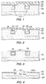
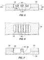
- the air bridge structure shown in Figures 5 and 6 is made in accordance with the process steps shown in Figures 1-4.
- a suitable silicon substrate 238 has a layer of silicon dioxide 236 deposited or grown on one surface. That surface is processed to form the air bridge structure of FigureS. 5 and 6
- trenches 220 are formed in an oxide layer 236 that covers substrate 238.
- the trenches 220 are coated with a layer of silicon nitride 247 or any other dielectric that can be selectively etched with respect to oxide layer 236.
- a layer of metal 242 is deposited on the surface and in the trenches 220.
- the surface is then coated with a layer of photoresist 250.
- the photoresist and metal layer are planarized by a reactive ion etch that uses the nitride layer 247 as an etch stop.
- the remaining photoresist is stripped and a second nitride layer is deposited to cover the metal in the trenches to form nitride sheaths 249 that surround the metal 242 in each trench.
- Another layer of photoresist 150 is deposited and patterned to protect the nitride layer 249.
- the exposed nitride on the surface is etched away leaving the sheath 249 around the conductors 242.
- the conductors 242 that remain may be partially imbedded in the insulative material layer 236 (the oxide) as shown in Figure. 4.
- the surface of the layer 236 may be masked with an etchant resistant mask 245 and then etched to form the cavity 240 and the cavity 244 as shown in Figure 5.
- FIG. 5 and 6 there is shown structure having a layer 236 of insulating material, such as oxide, and a substrate layer 238 of semiconductive material, such as silicon, in which integrated circuits may be formed.
- a layer 236 of insulating material such as oxide
- a substrate layer 238 of semiconductive material such as silicon
- Supported in the layer 236 and bridging an opening 240 therein are a plurality of conductors 242 which define air bridges for interconnecting integrated circuits (not shown) in the silicon substrate 238.
- a cavity 244 in the substrate 238 is disposed in alignment with the opening 240.
- the opening and the cavity provide an air dielectric which reduces parasitic capacitance between the circuits in the silicon substrate 238 and the air bridge conductors 242.
- Sheaths 249 around the conductors 242 protect the conductors against contamination or damage by, for example, flakes of conductive material which may be formed during the processing of the substrate 238 to provide the integrated circuits therein.
- Support posts 248 may be provided in the opening 240 and underlie the sheathed conductors 242.
- the support posts 248 provide added support for the conductors 242.
- a support post 248 may be aligned with the sheathed conductors 242.
- An anisotropic etch will remove silicon from areas not covered by the sheathed conductors to provide the supports 248 shown in Figure. 7.
- the support posts may also be formed only of the oxide layer 236.
- the posts are coated with a protective layer of nitride 258 as shown in Figure. 8.
- an aluminum conductor 250 rests on oxide support post 252.
- the post is passivated by depositing a sheath of nitride 258 or other passivating material, as shown in Figures 9B and 9C.
- the conductor may be passivated by oxidation to provide a layer 254 of aluminum oxide (Al 2 O 3 ) as shown in Figure. 10A.
- the metal conductor 242 or aluminum conductor 250 may be also be passivated by a sheath of silicon oxide 251 (SiO 2 ) covered by a sheath of polysilicon 256 ( Figure. 10B), thus providing a dual layer sheath.
- FIG. 11 there is shown another embodiment of the invention formed on a bonded substrate structure.
- a handle substrate 100 that is oxide bonded via oxide layer 102 to the device substrate 110.
- the device substrate 110 is patterned to form a series of trenches 101 to the surface of the bond oxide layer 102.
- an oxide layer 104 is either thermally grown or deposited over the surface of the device substrate and the trenches 101.
- the trenches 101 are filled with polysilicon 105 and planarized.
- Another layer of dielectric material e.g., silicon dioxide, is deposited.
- a layer of metal 106 is deposited and etched to form the conductors 106 over trenches 101.
- Another oxide layer 108 covers the metal.
- the structure of Figure. 14 is then masked and etched to provide the separated posts 116, 114, 112 of Figure. 15.
- the air between the separated posts reduces the capacitance between the conductors 106.
- the air bridge structure formed by the process of Figures 11-15 uses trench techniques compatible with customary bonded substrate processing.
- the air bridge structure is thus formed at the level of the device substrate 110 and is readily interconnected with circuits in the device substrate 110 by customary metallization and interconnect techniques.
- a device substrate 200 which is bonded to a handle substrate 202 via oxide bond layer 216.
- integrated circuits (not shown) and air bridge structure are formed.
- the device substrate contains an inductor coil 204 suspended over the interfacing surfaces 207 of the device substrate 200 and handle substrate 202 and separated therefrom by a space or void 206 which may be void except for posts 208.
- the coil 204 provides the inductor and may be of the square spiral shape shown in Figure 17.
- the center and end contacts 210 and 212 to the ends of the coil 204 do not appear in Figure 16. These contacts are of metal just like the coil turns and may extend along posts 208 to the active integrated circuits in the device substrate 200 in a manner similar to connections from the coils and the embodiments of the invention heretofore described.
- the coil 204 is an air bridge conductive element.
- the bridge end support for the element 204 is provided by a layer of dielectric material 205 having an extent beyond the outer periphery of the conductors of the coil 204. This bridge is also supported on the posts 208.
- Device substrate 200 has a bottom oxide layer 216.
- Oxide layer 216 bonds the device substrate 200 to the handle substrate 202.
- Another trench in a center post 208 may be filled with polysilicon in which case a pair of voids 206A and 206B may be formed in the substrate 200.
- the device substrate 200 is fabricated in process steps shown in Figures 18, 19 and 20.
- a device substrate 200 has a silicon substrate 220 covered with a layer of oxide 205 or other suitable dielectric that encases conductor coil 204.
- the coil 204 may be provided in a trench and then covered so as to form the layer of dielectric, insulating material 205.
- the coil 204 may be formed by depositing a metal layer on a dielectric layer, patterning the metal layer, and depositing a further layer of dielectric on the patterned metal layer.
- the device substrate is patterned to form trenches 106.
- the trenches are opened, coated with a thermal oxide 107 and filled with undoped polysilicon 108.
- the bond layer 216 joins the handle substrate 202 (not shown) to the device substrate 220.
- vias 224 and 226 are etched into the layer 205.
- the silicon of device substrate 220 is removed from the region between the trenches 106 by a selective etch to form the void 206.
- a cylindrical post 230 is provided by forming a via in the layer 205 and removing silicon in a region between the trenches 110, 112.
- the cavity between trenches 110 and 112 is filled with a ferromagnetic material such as iron.
- the ferromagnetic post 230 extends into the area of the inductor coil 204 and is electromagnetically coupled thereto so as to enhance and increase the inductance of the coil.
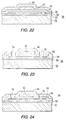
- An in-silicon air bridge as shown in Figure 24 may be formed by the process steps shown in Figures 22 and 23. Referring to Figures 24 and 25, there is shown another integrated circuit structure 54 with an air bridge conductor 42.
- the air bridge 42 is formed on a single semiconductor (silicon) substrate layer 52 having an insulative (SiO 2 ) layer 60 thereon.
- the active integrated circuits may be formed separately in the substrate 52 and have connections such as conductor 42 between devices of the integrated circuit.
- the silicon substrate 52 has an insulating layer 60, typically an oxide layer, either thermally grown or deposited.
- a sacrificial layer of polysilicon 68 or other material covers the insulating layer 60.
- the sacrificial layer 68 is patterned to the desired shape of an air bridge cavity and is covered with an oxide layer 64.
- a layer of metal 42 is deposited on oxide layer 64 and is patterned into the desired con Figureuration of the air bridge conductor.
- the patterned conductor 42 is covered with an insulating layer 44 of oxide or nitride.
- vias 74 and 76 are opened to remove the sacrificial polysilicon layer 68.
- a cavity 66 is created by etching and removing the polysilicon 68.
- Further vias 70, 72 are provided to contact the airbridge metal 42 as shown in Figure 25.
- FIG. 27 there is shown a structure similar to that shown in Figure 24 and like parts are labeled with like referenced numerals.
- a layer of sacrificial polysilicon or metal which is shown at 68 in Figure 26, is used.
- the surface oxide layer 60 is patterned to remove a portion of oxide layer 60.
- a sacrificial polysilicon layer 68 is deposited over the exposed substrate.
- the polysilicon layer 68 is covered with an oxide layer 64.
- the air bridge metal 42 is deposited on the oxide layer 64 patterned and covered with another oxide layer 44.
- Etch windows 74 and 76 provide etch holes for an etchant, for example, KOH, which etches the polysilicon metal 68 isotropically, but etches the silicon in the substrate 52 anisotropically thereby producing a deep cavity 66A.
- the anisotropic etching process to produce the deep void or cavity 66A may be carried out in accordance with the etch/removal method described in an article by Sugiyama, et al., entitled “Micro-diaphragm Pressure Sensor," IEDM 1986, pages 184-187.
- the void space 66A is aligned with the conductive element of the air bridge structure 42 and is operative to reduce parasitic capacitances in the device.
- Removing silicon not only reduces capacitance but also reduces parasitic image current induced in the silicon by currents flowing in a conductor above the silicon. Such induced current is reduced by the voids that space the conductors from the silicon.
- the devices are fabricated at the substrate level and then separated into dice having one or more active integrated circuits using scribes or trenches of the type conventionally used for die separation.
- Conductive elements may be incorporated in the devices at the integrated circuit leve.
- An elongated conductor is formed over the dielectric layer and is encased in dielectric material. Then, portions of the substrate or the dielectric layer, or both, are removed to expose the encased elongated conductor to air.
- the method contemplates using sacrificial materials located between the encased conductor in the substrate. Removing the sacrificial material forms an air bridge cavity. The methods of the invention also include removing portions of the substrate in order to form the air bridge cavity.
- a device substrate is bonded to a handle substrate, typically with an oxide bonding layer. Trench isolation is a common step used in the formation of devices and bonded substrates.
- the air bridge of the invention is compatible with the trench forming steps that are typically used in bonded substrates.
- trenches are formed down to the oxide bonding layer.
- the trenches are coated with a dielectric, filled, and planarized.
- the dielectric layer covers the planarized trenches and elongated conductors are patterned on the dielectric layer over the air bridge trenches.
- Another dielectric layer covers the patterned conductors in order to encase them in a dielectric.
- the substrate is further patterned and etched to remove material from between the filled air bridge trenches.
- the final structure provides air bridge conductors encased in a dielectric that is spaced from the bonding oxide layer.
Abstract
Conductive elements may be incorporated in the devices at the integrated circuit level. An elongated conductor is formed over the dielectric layer and is encased in dielectric material. Then, portions of the substrate or the dielectric layer, or both, are removed to expose the encased elongated conductor to air. The method contemplates using sacrificial materials located between the encased conductor in the substrate. Removing the sacrificial material forms an air bridge cavity. The methods of the invention also include removing portions of the substrate in order to form the air bridge cavity. In a bonded substrate structure, a device substrate is bonded to a handle substrate, typically with an oxide bonding layer. Trench isolation is a common step used in the formation of devices and bonded substrates. The air bridge of the invention is compatible with the trench forming steps that are typically used in bonded substrates. In one bonded substrate embodiment, trenches are formed down to the oxide bonding layer. The trenches are coated with a dielectric, filled, and planarized. The dielectric layer covers the planarized trenches and elongated conductors are patterned on the dielectric layer over the air bridge trenches. Another dielectric layer covers the patterned conductors in order to encase them in a dielectric. Then the substrate is further patterned and etched to remove material from between the filled air bridge trenches. The final structure provides air bridge conductors encased in a dielectric that is spaced from the bonding oxide layer.
Description
- The present invention relates to integrated circuit air bridge structures and methods of fabricating such structures which are hermetically sealed so as to protect the integrated circuits and any components, such as interconnecting conductors air bridges, inductors or capacitors, against damage or contamination from outside the device.
- In order to reduce interconnect capacitances in high performance and high frequency processes, air bridges are often used. A typical air bridge is formed using a second layer of interconnect metal deposited and patterned over a sacrificial material. The sacrificial material is later removed to leave a metal lead surrounded by air rather than a dielectric, such as oxide. The capacitances to the substrate and to other metal lead is thus reduced since air has a lower dielectric constant than do solid insulators such as silicon dioxide or silicon nitride.
- However, traditional air bridge manufacturing techniques and structures have several disadvantages. The length of an air bridge is often limited by flexure of metal between two vias. So, relatively long air bridges can only be manufactured by stitching together multiple lengths of short air bridges. Another problem is that circuits fabricated with air bridges cannot be passivated. In a normal process, a passivation layer is deposited on top of an integrated circuit. Typical passivation layers are silicon oxide or silicon nitride. However, for air bridge structures, the passivation layer has to be omitted otherwise the passivation layer will fill the air under the bridge and thereby increase the capacitance of the air bridge or damage the bridge itself.
- Accordingly, there has arisen a need for air bridges that can be made of longer lengths of metal than are available in air bridges of the prior art and also for air bridges that can be incorporated into integrated circuits where such circuits have a passivation layer.
- An object of the present invention is to provide improved integrated circuit air bridge structures which may be fabricated at the substrate level and which are passivated in the course of fabrication thereby avoiding the need for ceramic packaging or encapsulation, without materially increasing the volume occupied by the integrated circuit and any components, and to provide improved integrated circuit air bridge structures having air bridges or other components made out of conductive elements (e.g., inductors or capacitors), wherein sufficient spacing is provided between the air bridges of the components and the active integrated circuit so as to reduce the effect of parasitic capacitance between the conductive elements and the circuits and adversely affecting the high frequency response of these circuits.
- An integrated circuit structure in accordance with the invention provides an air bridge fabricated on the same die as the integrated circuit to which the air bridge is connected. The invention provides an on-silicon air bridge that is compatible with single substrate and bonded substrate structures. The invention provides an air bridge structure on a semiconductor substrate or a device substrate. The device or semiconductor substrate may have one or more integrated circuits or semiconductor devices formed therein. The air bridge structure comprises an elongated metal conductor that is encased in a dielectric sheath. At least a portion of the sheath is exposed to ambient atmosphere. In one embodiment, the entire sheath is exposed to atmosphere. However, other embodiments expose a substantial portion of the sheath to ambient atmosphere in order to reduce the dielectric coupling between the sheath and the semiconductor substrate. In a typical construction, the encased conductor crosses a cavity in the substrate. The encased conductor is supported in its transit across the cavity by posts that extend from the lower surface of the cavity. The support posts comprise dielectric material, substrate material, or both.
- The air bridge structure is made by forming a dielectric layer over semiconductor substrate. An elongated conductor is formed over the dielectric layer and is encased in dielectric material. Then, portions of the substrate or the dielectric layer, or both, are removed to expose the encased elongated conductor to air. The method contemplates using sacrificial materials located between the encased conductor in the substrate. Removing the sacrificial material forms an air bridge cavity. The methods of the invention also include removing portions of the substrate in order to form the air bridge cavity.
- Particular embodiments of the invention include a cavity formed in the substrate and/or in the dielectric layer on the substrate. The encased conductors extend across the cavity and enter and exit the dielectric layer overlying the cavity.
- In a bonded substrate structure, a device substrate is bonded to a handle substrate, typically with an oxide bonding layer. An air bridge structure is formed in the device substrate in several ways. Trench isolation is a common step used in the formation of devices and bonded substrates. The air bridge of the invention is compatible with the trench forming steps that are typically used in bonded substrates. In one bonded substrate embodiment, trenches are formed down to the oxide bonding layer. The trenches are coated with a dielectric, filled, and planarized. The dielectric layer covers the planarized trenches and elongated conductors are patterned on the dielectric layer over the air bridge trenches. Another dielectric layer covers the patterned conductors in order to encase them in a dielectric. Then the substrate is further patterned and etched to remove material from between the filled air bridge trenches. The final structure provides air bridge conductors encased in a dielectric that is spaced from the bonding oxide layer.
- Bonded substrate structures are used to form inductors. In one embodiment, elongated conductors are encased in a dielectric layer that is disposed over a device substrate region located between isolating trenches. Vias are opened in the dielectric layer and substrate material is removed to form an air bridge cavity beneath the encased conductors. Two air bridge cavities may be formed near one another and separated by a third cavity. Over each air bridge cavity conductors are patterned in a continuous, spiral path of metal in order to form an inductors. The third cavity is filled with ferromagnetic material.
- Two further embodiments of the invention use a sacrificial layer for forming a cavity beneath an elongated, encased conductor. In one embodiment, a sacrificial layer of polysilicon is formed over a first dielectric layer that is on the semiconductor substrate. An encased conductor is formed over the sacrificial layer. Vias are opened to the sacrificial polysilicon and the polysilicon is removed to leave an air bridge cavity beneath the encased conductor and between the encased conductor and the silicon substrate. In an alternate embodiment, the dielectric layer on the surface of the substrate is partially removed before the sacrificial polysilicon is deposited. The sacrificial polysilicon is removed along with portions of the underlying substrate. The latter provides an enlarged air bridge cavity beneath the encased conductor.
- The present invention includes an air bridge structure in a semiconductor substrate having one or more integrated circuits or semiconductor devices therein comprising an elongated metal conductor having a dielectric coating around at least a portion of the length of said conductor, said sheath being exposed to ambient atmosphere.
- The invention also includes a method for forming an air bridge conductor comprising the steps of, depositing a dielectric layer over a semiconductor substrate, forming an elongated conductor over the substrate, encasing the elongated conductor in a dielectric sheath, and removing a portion of one or more layers proximate the sheathed conductor to form an air bridge conductor.
- The invention will now be described by way of exmple with reference to the accompanying drawings in which
- Figures 1-4 show the device illustrated in Figure 5 in successive stages of the fabrication thereof;
- Figure 5 is a sectional view of a portion of an integrated circuit device having conductive members disposed in so-called "air bridge" configuration over an open space within the device;
- Figure 6 is a fragmentary plan view illustrating the portion of the device shown in Figure 5; the view being taken along the line 6-6 in Figure 5;
- Figures 7 and 8 illustrate a device similar to that shown in Figure 5;
- Figures 9A-9C and 10A, 10B are fragmentary views, the view in Figures 9C being taken along the
line 9C-9C in Figure 9B, the views illustrating means for support of conductive elements in the open space of an integrated circuit device; - Figures 11-15 show progressive steps in the formation of a bonded substrate with an air bridge formed in the device substrate;
- Figure 16 is a fragmentary, sectional view of a portion of an enclosed, multi-layer integrated circuit device where a conductive member forming an inductor is located over an open space, all in accordance with still another embodiment of the invention, which provides contamination and damage protection and ease of handling during manufacture of integrated circuit devices, the view being taken along the line 16-16 in Figure 17;
- Figure 17 is a plan view of the portion of the device shown in Figure 16;
- Figures 18 to 20 are sectional views illustrating the device shown in Figures 16 and 17 in successive stages of the manufacture thereof;
- Figure 21 is a sectional view of a device similar to that shown in Figure 16 wherein an internal core of ferromagnetic material is provided within the device;
- Figures 22 and 23 are sectional views of the device shown in Figure 24 during an earlier and later stage in the fabrication thereof;
- Figure 24 is a sectional view of a portion of an integrated circuit device of bonded layers including a conductive layer providing an interconnection suspended and bridging an open space in the device;
- Figure 25 is a fragmentary plan view of the portion of the device shown in Figure 24;
- Figure 26 is a sectional view of a portion of a bonded, enclosed, multi-layer device having a conductive layer which provides an interconnection over an open space in the device in accordance with another embodiment of the invention;
- Figure 27 is a sectional view of the device shown in Figure 26 in a later stage of manufacture.
- The air bridge structure shown in Figures 5 and 6 is made in accordance with the process steps shown in Figures 1-4. A
suitable silicon substrate 238 has a layer ofsilicon dioxide 236 deposited or grown on one surface. That surface is processed to form the air bridge structure of FigureS. 5 and 6 - By referring to Figures 1-4, the steps in the process of fabricating the devices of Figures 5 and 6 will become more apparent. First,
trenches 220 are formed in anoxide layer 236 that coverssubstrate 238. Thetrenches 220 are coated with a layer ofsilicon nitride 247 or any other dielectric that can be selectively etched with respect tooxide layer 236. Next, a layer ofmetal 242 is deposited on the surface and in thetrenches 220. The surface is then coated with a layer ofphotoresist 250. The photoresist and metal layer are planarized by a reactive ion etch that uses thenitride layer 247 as an etch stop. After the etch, the remaining photoresist is stripped and a second nitride layer is deposited to cover the metal in the trenches to formnitride sheaths 249 that surround themetal 242 in each trench. Another layer of photoresist 150 is deposited and patterned to protect thenitride layer 249. The exposed nitride on the surface is etched away leaving thesheath 249 around theconductors 242. Theconductors 242 that remain may be partially imbedded in the insulative material layer 236 (the oxide) as shown in Figure. 4. As also shown in Figure. 4, the surface of thelayer 236 may be masked with an etchantresistant mask 245 and then etched to form thecavity 240 and thecavity 244 as shown in Figure 5. - Referring to Figures 5 and 6 there is shown structure having a
layer 236 of insulating material, such as oxide, and asubstrate layer 238 of semiconductive material, such as silicon, in which integrated circuits may be formed. Supported in thelayer 236 and bridging anopening 240 therein are a plurality ofconductors 242 which define air bridges for interconnecting integrated circuits (not shown) in thesilicon substrate 238. Acavity 244 in thesubstrate 238 is disposed in alignment with theopening 240. The opening and the cavity provide an air dielectric which reduces parasitic capacitance between the circuits in thesilicon substrate 238 and theair bridge conductors 242.Sheaths 249 around theconductors 242 protect the conductors against contamination or damage by, for example, flakes of conductive material which may be formed during the processing of thesubstrate 238 to provide the integrated circuits therein. - Support posts 248 (Figure.7) may be provided in the
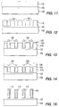
opening 240 and underlie the sheathedconductors 242. The support posts 248 provide added support for theconductors 242. Asupport post 248 may be aligned with the sheathedconductors 242. An anisotropic etch will remove silicon from areas not covered by the sheathed conductors to provide thesupports 248 shown in Figure. 7. - The support posts may also be formed only of the
oxide layer 236. The posts are coated with a protective layer ofnitride 258 as shown in Figure. 8. - Referring to Figure. 9A an
aluminum conductor 250 rests onoxide support post 252. The post is passivated by depositing a sheath ofnitride 258 or other passivating material, as shown in Figures 9B and 9C. The conductor may be passivated by oxidation to provide alayer 254 of aluminum oxide (Al2O3) as shown in Figure. 10A. Themetal conductor 242 oraluminum conductor 250 may be also be passivated by a sheath of silicon oxide 251 (SiO2) covered by a sheath of polysilicon 256 (Figure. 10B), thus providing a dual layer sheath. - Turning to Figures 11-15, there is shown another embodiment of the invention formed on a bonded substrate structure. In Figure 11 there is a
handle substrate 100 that is oxide bonded viaoxide layer 102 to thedevice substrate 110. In a following step (Figure 12), thedevice substrate 110 is patterned to form a series oftrenches 101 to the surface of thebond oxide layer 102. Next, (Figure. 13) anoxide layer 104 is either thermally grown or deposited over the surface of the device substrate and thetrenches 101. Thetrenches 101 are filled withpolysilicon 105 and planarized. Another layer of dielectric material, e.g., silicon dioxide, is deposited. A layer ofmetal 106 is deposited and etched to form theconductors 106 overtrenches 101. Anotheroxide layer 108 covers the metal. The structure of Figure. 14 is then masked and etched to provide the separatedposts conductors 106. So, the air bridge structure formed by the process of Figures 11-15 uses trench techniques compatible with customary bonded substrate processing. The air bridge structure is thus formed at the level of thedevice substrate 110 and is readily interconnected with circuits in thedevice substrate 110 by customary metallization and interconnect techniques. - Referring to Figures 16 and 17 there is shown a
device substrate 200 which is bonded to ahandle substrate 202 viaoxide bond layer 216. Indevice substrate 200 integrated circuits (not shown) and air bridge structure are formed. The device substrate contains aninductor coil 204 suspended over the interfacing surfaces 207 of thedevice substrate 200 and handlesubstrate 202 and separated therefrom by a space or void 206 which may be void except forposts 208. - The
coil 204 provides the inductor and may be of the square spiral shape shown in Figure 17. The center and endcontacts coil 204 do not appear in Figure 16. These contacts are of metal just like the coil turns and may extend alongposts 208 to the active integrated circuits in thedevice substrate 200 in a manner similar to connections from the coils and the embodiments of the invention heretofore described. - The
coil 204 is an air bridge conductive element. The bridge end support for theelement 204 is provided by a layer ofdielectric material 205 having an extent beyond the outer periphery of the conductors of thecoil 204. This bridge is also supported on theposts 208. -
Device substrate 200 has abottom oxide layer 216.Oxide layer 216 bonds thedevice substrate 200 to thehandle substrate 202. Another trench in acenter post 208 may be filled with polysilicon in which case a pair ofvoids substrate 200. - The
device substrate 200 is fabricated in process steps shown in Figures 18, 19 and 20. Adevice substrate 200 has asilicon substrate 220 covered with a layer ofoxide 205 or other suitable dielectric that encasesconductor coil 204. Thecoil 204 may be provided in a trench and then covered so as to form the layer of dielectric, insulatingmaterial 205. As an alternative, thecoil 204 may be formed by depositing a metal layer on a dielectric layer, patterning the metal layer, and depositing a further layer of dielectric on the patterned metal layer. - As shown in Figure 19 the device substrate is patterned to form
trenches 106. The trenches are opened, coated with athermal oxide 107 and filled withundoped polysilicon 108. Thebond layer 216 joins the handle substrate 202 (not shown) to thedevice substrate 220. As shown in Figure 20vias layer 205. The silicon ofdevice substrate 220 is removed from the region between thetrenches 106 by a selective etch to form thevoid 206. - Referring to Figure 21 there is shown a structure similar to that shown in Figure 16 and like parts are indicated with like referenced numerals. A
cylindrical post 230 is provided by forming a via in thelayer 205 and removing silicon in a region between thetrenches trenches ferromagnetic post 230 extends into the area of theinductor coil 204 and is electromagnetically coupled thereto so as to enhance and increase the inductance of the coil. - An in-silicon air bridge as shown in Figure 24 may be formed by the process steps shown in Figures 22 and 23. Referring to Figures 24 and 25, there is shown another integrated
circuit structure 54 with anair bridge conductor 42. Theair bridge 42 is formed on a single semiconductor (silicon)substrate layer 52 having an insulative (SiO2)layer 60 thereon. - As shown in Figures 22 and 23, the active integrated circuits may be formed separately in the
substrate 52 and have connections such asconductor 42 between devices of the integrated circuit. Thesilicon substrate 52 has an insulatinglayer 60, typically an oxide layer, either thermally grown or deposited. A sacrificial layer ofpolysilicon 68 or other material covers the insulatinglayer 60. Thesacrificial layer 68 is patterned to the desired shape of an air bridge cavity and is covered with anoxide layer 64. A layer ofmetal 42 is deposited onoxide layer 64 and is patterned into the desired conFigureuration of the air bridge conductor. The patternedconductor 42 is covered with an insulatinglayer 44 of oxide or nitride. - As shown in Figure 23, vias 74 and 76 are opened to remove the
sacrificial polysilicon layer 68. Acavity 66 is created by etching and removing thepolysilicon 68.Further vias airbridge metal 42 as shown in Figure 25. - Referring to Figure 27, there is shown a structure similar to that shown in Figure 24 and like parts are labeled with like referenced numerals. Again, a layer of sacrificial polysilicon or metal, which is shown at 68 in Figure 26, is used. First, the
surface oxide layer 60 is patterned to remove a portion ofoxide layer 60. Asacrificial polysilicon layer 68 is deposited over the exposed substrate. Thepolysilicon layer 68 is covered with anoxide layer 64. theair bridge metal 42 is deposited on theoxide layer 64 patterned and covered with anotheroxide layer 44.Etch windows polysilicon metal 68 isotropically, but etches the silicon in thesubstrate 52 anisotropically thereby producing adeep cavity 66A. The anisotropic etching process to produce the deep void orcavity 66A may be carried out in accordance with the etch/removal method described in an article by Sugiyama, et al., entitled "Micro-diaphragm Pressure Sensor," IEDM 1986, pages 184-187. Thevoid space 66A is aligned with the conductive element of theair bridge structure 42 and is operative to reduce parasitic capacitances in the device. Removing silicon not only reduces capacitance but also reduces parasitic image current induced in the silicon by currents flowing in a conductor above the silicon. Such induced current is reduced by the voids that space the conductors from the silicon. The devices are fabricated at the substrate level and then separated into dice having one or more active integrated circuits using scribes or trenches of the type conventionally used for die separation. - Conductive elements may be incorporated in the devices at the integrated circuit leve. An elongated conductor is formed over the dielectric layer and is encased in dielectric material. Then, portions of the substrate or the dielectric layer, or both, are removed to expose the encased elongated conductor to air. The method contemplates using sacrificial materials located between the encased conductor in the substrate. Removing the sacrificial material forms an air bridge cavity. The methods of the invention also include removing portions of the substrate in order to form the air bridge cavity. In a bonded substrate structure, a device substrate is bonded to a handle substrate, typically with an oxide bonding layer. Trench isolation is a common step used in the formation of devices and bonded substrates. The air bridge of the invention is compatible with the trench forming steps that are typically used in bonded substrates. In one bonded substrate embodiment, trenches are formed down to the oxide bonding layer. The trenches are coated with a dielectric, filled, and planarized. The dielectric layer covers the planarized trenches and elongated conductors are patterned on the dielectric layer over the air bridge trenches. Another dielectric layer covers the patterned conductors in order to encase them in a dielectric. Then the substrate is further patterned and etched to remove material from between the filled air bridge trenches. The final structure provides air bridge conductors encased in a dielectric that is spaced from the bonding oxide layer.
Claims (16)
- An air bridge structure in a semiconductor substrate having one or more integrated circuits or semiconductor devices therein comprising an elongated metal conductor having a dielectric coating around at least a portion of the length of said conductor, said sheath being exposed to ambient atmosphere.
- An air bridge structure as claimed in claim 1 wherein the dielectric coating comprises a dielectric selected from the group consisting of silicon dioxide, silicon nitride, and aluminum oxide, and the conductor comprises aluminum.
- An air abridge structure as claimed in claims 1 or 2, characterized by a support extending from a surface of the semiconductor substrate to the outer surface of the sheath for supporting the conductor.
- An air bridge structure as claimed in claim 3 wherein the support comprises semiconductor material.
- An air bridge structure as claimed in any one of claims 1 to 4 wherein a majority of the entire outer surface area of a portion of the sheath is exposed to ambient atmosphere.
- An air bridge structure as claimed in claim 5 wherein the conductor is disposed opposite a cavity in the semiconductor substrate.
- An air bridge as claimed in claim 6 wherein said conductor is formed into a spiral of adjacent turns to create an inductor, and the dielectric coating comprises a dielectric layer and an inductor is formed in the dielectric layer over a cavity in the semiconductor substrate.
- An air bridge as claimed in claim 7 characterized int that at least a second inductor spaced from the first inductor by a core cavity, said core cavity is filled with ferromagnetic material.
- An air bridge structure comprising:a bonded substrate structure comprising a device substrate having an upper and lower surface with one or more semiconductor devices or integrated circuits formed in said device substrate, a handle substrate, and a bonding layer for bonding the lower surface of the device substrate to the handle substrate;a cavity in said device substrate extending from the upper surface of the device substrate to the bonding layera post comprising an elongated strip of dielectric material extending from the bonding layer to about the upper surface of the device substrate;a conductor encased in said elongated strip.
- An air bridge structure as claimed in claim 9 wherein the post further comprises an elongated region of polysilicon disposed between the conductor and the bonding layer.
- A method for forming an air bridge conductor comprising the steps of:depositing a dielectric layer over a semiconductor substrate;forming an elongated conductor over the substrate;encasing the elongated conductor in a dielectric sheath;removing a portion of one or more layers proximate the sheathed conductor to form an air bridge conductor.
- A method as claimed in claim 11 wherein the portions removed comprise portions of the first dielectric layer, and additional portions removed comprises portions of the semiconductor substrate.
- A method as claimed in claims 11 or 12 characterized by the step of depositing a sacrificial layer between the encased conductor and the semiconductor substrate and removing a portion of the sacrificial layer to form an air bridge cavity.
- A method for forming an air bridge comprising the steps of:bonding a device substrate to a handle substrate using an oxide bonding layer;forming a plurality of trenches in the device substrate and extending to the oxide bonding layer;coating the trenches with a first dielectric layer;filling and planarizing the trenches to the level of the device substrate;depositing a second dielectric layer over the planarized device substrate;depositing a metal layer on the second dielectric layer;patterning the metal layer to form conductors over the filled trenches;covering the conductors with a third layer of dielectric;selectively removing the dielectric material and the device substrate material from regions between the filled trenches to form air bridge conductors spaced from the bonding layer, encased in dielectric and laterally separated by ambient atmosphere.
- A method as claimed in claim 14 characterized by the step of filling the coated trenches with polysilicon before planarizing.
- A method as claimed in claims 14 or 15 characterized by forming first and second air bridge cavities with a single conductors extending in a spiral path across each cavity and encased in dielectric;forming a third cavity between the first and second air bridge cavities;filling the third cavity with ferromagnetic material.
Applications Claiming Priority (2)
| Application Number | Priority Date | Filing Date | Title |
|---|---|---|---|
| US658010 | 1996-06-04 | ||
| US08/658,010 US6492705B1 (en) | 1996-06-04 | 1996-06-04 | Integrated circuit air bridge structures and methods of fabricating same |
Publications (1)
| Publication Number | Publication Date |
|---|---|
| EP0812016A1 true EP0812016A1 (en) | 1997-12-10 |
Family
ID=24639540
Family Applications (1)
| Application Number | Title | Priority Date | Filing Date |
|---|---|---|---|
| EP97108480A Withdrawn EP0812016A1 (en) | 1996-06-04 | 1997-05-26 | Integrated circuit air bridge structures and methods of fabricating same |
Country Status (6)
| Country | Link |
|---|---|
| US (2) | US6492705B1 (en) |
| EP (1) | EP0812016A1 (en) |
| JP (1) | JPH1092932A (en) |
| KR (1) | KR980006111A (en) |
| CN (1) | CN1167340A (en) |
| TW (1) | TW424295B (en) |
Cited By (14)
| Publication number | Priority date | Publication date | Assignee | Title |
|---|---|---|---|---|
| EP0915513A1 (en) * | 1997-10-23 | 1999-05-12 | STMicroelectronics S.r.l. | High quality factor, integrated inductor and production method thereof |
| EP0932189A2 (en) * | 1998-01-22 | 1999-07-28 | Raytheon Company | Inductor structure with air dielectric |
| WO2000024042A1 (en) * | 1998-10-21 | 2000-04-27 | Micronas Munich Gmbh | Arrangement with at least one integrated inductive element on a substrate |
| WO2000051177A1 (en) * | 1999-02-26 | 2000-08-31 | Advanced Micro Devices, Inc. | Integrated circuit device with air dielectric |
| WO2001095390A1 (en) * | 2000-06-02 | 2001-12-13 | Sumitomo Precision Products Co., Ltd. | Semiconductor device and method of manufacturing the device |
| WO2002058551A3 (en) * | 2001-01-22 | 2002-10-24 | Integrated Sensing Systems Iss | Wireless mems capacitive sensor for physiologic parameter measurement |
| FR2841381A1 (en) * | 2002-06-24 | 2003-12-26 | Nec Electronics Corp | INTEGRATED SEMICONDUCTOR CIRCUIT AND A METHOD FOR MANUFACTURING THE CIRCUIT |
| SG108812A1 (en) * | 1999-10-07 | 2005-02-28 | Chartered Semiconductor Mfg | A method to fabricate horizontal air columns underneath metal inductor |
| WO2007029178A3 (en) * | 2005-09-06 | 2007-06-07 | Nxp Bv | Method of manufacturing a semiconductor device with an isolation region and a device manufactured by the method |
| EP1935022A2 (en) * | 2005-09-30 | 2008-06-25 | Freescale Semiconductor, Inc. | Microelectronic assembly and method for forming the same |
| EP1935008A2 (en) * | 2005-09-30 | 2008-06-25 | Freescale Semiconductor, Inc. | Microelectronic assembly and method for forming the same |
| WO2010076187A2 (en) * | 2008-12-30 | 2010-07-08 | Stmicroelectronics S.R.L. | Integrated electronic device with transceiving antenna and magnetic interconnection |
| US8267863B2 (en) | 2007-04-30 | 2012-09-18 | Integrated Sensing Systems, Inc. | Procedure and system for monitoring a physiological parameter within an internal organ of a living body |
| CN113764261A (en) * | 2020-10-15 | 2021-12-07 | 腾讯科技(深圳)有限公司 | Air bridge structure and manufacturing method thereof, superconducting quantum chip and manufacturing method thereof |
Families Citing this family (40)
| Publication number | Priority date | Publication date | Assignee | Title |
|---|---|---|---|---|
| EP0996157B1 (en) * | 1998-10-21 | 2005-08-03 | STMicroelectronics S.r.l. | Process for manufacturing integrated devices comprising microstructures and associated suspended electrical interconnections |
| US6551924B1 (en) * | 1999-11-02 | 2003-04-22 | International Business Machines Corporation | Post metalization chem-mech polishing dielectric etch |
| KR100369324B1 (en) * | 1999-12-02 | 2003-01-24 | 한국전자통신연구원 | Method for fabricating planar type micro cavity |
| EP1130631A1 (en) * | 2000-02-29 | 2001-09-05 | STMicroelectronics S.r.l. | Process for forming a buried cavity in a semiconductor material wafer |
| US7230315B2 (en) * | 2000-02-29 | 2007-06-12 | Stmicroelectronics S.R.L. | Integrated chemical microreactor with large area channels and manufacturing process thereof |
| US7732192B2 (en) * | 2000-02-29 | 2010-06-08 | Stmicroelectronics S.R.L. | Integrated chemical microreactor with large area channels and manufacturing process thereof |
| SG98398A1 (en) * | 2000-05-25 | 2003-09-19 | Inst Of Microelectronics | Integrated circuit inductor |
| US6798064B1 (en) * | 2000-07-12 | 2004-09-28 | Motorola, Inc. | Electronic component and method of manufacture |
| US6489663B2 (en) * | 2001-01-02 | 2002-12-03 | International Business Machines Corporation | Spiral inductor semiconducting device with grounding strips and conducting vias |
| US6800918B2 (en) * | 2001-04-18 | 2004-10-05 | Intel Corporation | EMI and noise shielding for multi-metal layer high frequency integrated circuit processes |
| KR100382765B1 (en) * | 2001-06-15 | 2003-05-09 | 삼성전자주식회사 | Passive devices and modules for transceiver and manufacturing method thereof |
| US6858888B2 (en) * | 2001-11-26 | 2005-02-22 | Wisconsin Alumni Research Foundation | Stress control of semiconductor microstructures for thin film growth |
| US20040027846A1 (en) * | 2002-08-06 | 2004-02-12 | Thaddeus Schroeder | Method for forming ferromagnetic targets for position sensors |
| US20040195650A1 (en) * | 2003-04-04 | 2004-10-07 | Tsung-Ju Yang | High-Q inductor device with a shielding pattern embedded in a substrate |
| US20040238950A1 (en) * | 2003-05-30 | 2004-12-02 | Agency For Science, Technology And Research | Tunable low loss transmission lines |
| US7075167B2 (en) * | 2003-08-22 | 2006-07-11 | Agere Systems Inc. | Spiral inductor formed in a semiconductor substrate |
| US7084479B2 (en) * | 2003-12-08 | 2006-08-01 | International Business Machines Corporation | Line level air gaps |
| DE60312872T2 (en) * | 2003-12-10 | 2007-07-12 | Freescale Semiconductor, Inc., Austin | Method of making an element containing an electrical conductor surrounded by magnetic material |
| US7255801B2 (en) * | 2004-04-08 | 2007-08-14 | Taiwan Semiconductor Manufacturing Company, Ltd. | Deep submicron CMOS compatible suspending inductor |
| DE102004022139B4 (en) * | 2004-05-05 | 2007-10-18 | Atmel Germany Gmbh | A method for producing a spiral inductance on a substrate and a device produced by such a method |
| KR100548388B1 (en) * | 2004-07-20 | 2006-02-02 | 삼성전자주식회사 | Inductor element having high quality factor and a fabrication mentod thereof |
| US7190007B2 (en) * | 2004-08-05 | 2007-03-13 | International Business Machines Corporation | Isolated fully depleted silicon-on-insulator regions by selective etch |
| KR100712517B1 (en) * | 2005-07-14 | 2007-04-30 | 삼성전자주식회사 | Interposer of semiconductor device having air gap structure |
| JP4957951B2 (en) * | 2006-03-30 | 2012-06-20 | 日本電気株式会社 | Semiconductor device and manufacturing method thereof |
| CN101373734B (en) * | 2007-08-22 | 2011-03-16 | 中国科学院半导体研究所 | Method for preparing nanometer dimension nickel-gold air bridge |
| JP4815623B2 (en) * | 2007-09-07 | 2011-11-16 | 三菱電機株式会社 | High frequency passive device and method for manufacturing the same |
| US20090139749A1 (en) * | 2007-10-18 | 2009-06-04 | Long-Sheng Fan | Method For The Preparation Of A Flexible Transducer Unit, The Flexible Transducer Unit So Prepared And An Array Containing Such Flexible Transducer Units |
| US7897477B2 (en) * | 2009-01-21 | 2011-03-01 | Taiwan Semiconductor Manufacturing Company, Ltd. | Method of forming an isolation structure |
| US8003516B2 (en) * | 2009-08-26 | 2011-08-23 | International Business Machines Corporation | BEOL interconnect structures and related fabrication methods |
| US8703517B2 (en) * | 2010-10-29 | 2014-04-22 | Denso Corporation | Method of Manufacturing a Semiconductor Device Including Removing a Reformed Layer |
| US8754338B2 (en) * | 2011-05-28 | 2014-06-17 | Banpil Photonics, Inc. | On-chip interconnects with reduced capacitance and method of afbrication |
| DE102011080978B4 (en) * | 2011-08-16 | 2020-03-19 | Robert Bosch Gmbh | Method for producing a micromechanical structure |
| DE102014105077B4 (en) * | 2013-04-18 | 2024-01-18 | Infineon Technologies Austria Ag | Method for producing semiconductor components with a glass substrate, and semiconductor component |
| US9460996B1 (en) * | 2015-08-05 | 2016-10-04 | Globalfoundries Inc. | Integrated device with inductive and capacitive portions and fabrication methods |
| JP6657970B2 (en) * | 2016-01-07 | 2020-03-04 | 富士通株式会社 | Semiconductor device, manufacturing method thereof, and communication device |
| US9837485B2 (en) * | 2016-04-05 | 2017-12-05 | International Business Machines Corporation | High-density MIM capacitors |
| KR102606784B1 (en) * | 2018-07-13 | 2023-11-28 | 에스케이하이닉스 주식회사 | Semiconductor device with air gap and method for fabricating the same |
| US11699662B2 (en) | 2020-01-23 | 2023-07-11 | Nvidia Corporation | Face-to-face dies with probe pads for pre-assembly testing |
| US11616023B2 (en) * | 2020-01-23 | 2023-03-28 | Nvidia Corporation | Face-to-face dies with a void for enhanced inductor performance |
| US11127719B2 (en) | 2020-01-23 | 2021-09-21 | Nvidia Corporation | Face-to-face dies with enhanced power delivery using extended TSVS |
Citations (4)
| Publication number | Priority date | Publication date | Assignee | Title |
|---|---|---|---|---|
| EP0043014A2 (en) * | 1980-06-16 | 1982-01-06 | Rockwell International Corporation | Integrated circuit chip transmission line |
| EP0076935A2 (en) * | 1981-10-09 | 1983-04-20 | Honeywell Inc. | Integrated semiconductor device and method of fabricating said device |
| EP0523450A1 (en) * | 1991-07-03 | 1993-01-20 | Sumitomo Electric Industries, Ltd. | Inductance element |
| WO1994017558A1 (en) * | 1993-01-29 | 1994-08-04 | The Regents Of The University Of California | Monolithic passive component |
Family Cites Families (11)
| Publication number | Priority date | Publication date | Assignee | Title |
|---|---|---|---|---|
| US3786560A (en) * | 1972-03-20 | 1974-01-22 | J Cunningham | Electrical isolation of circuit components of integrated circuits |
| SE446826B (en) | 1981-04-24 | 1986-10-13 | Icab Ind Coating Ab | POWDER SPRAY WITH ELECTROSTATIC CHARGING FORM CONSISTING OF LONG-TERM CROCHET CHARGING CHANNELS WHICH ARE CROSSED TO IMAGE LOOP OR CARS ORGANIZED IN A MULTIPLE GROUPS |
| JPH0377360A (en) * | 1989-08-18 | 1991-04-02 | Mitsubishi Electric Corp | Semiconductor device |
| US5227658A (en) * | 1991-10-23 | 1993-07-13 | International Business Machines Corporation | Buried air dielectric isolation of silicon islands |
| EP0562207B1 (en) * | 1992-03-27 | 1996-06-05 | International Business Machines Corporation | Method of forming thin film pseudo-planar PFET devices and structures resulting therefrom |
| US5370766A (en) * | 1993-08-16 | 1994-12-06 | California Micro Devices | Methods for fabrication of thin film inductors, inductor networks and integration with other passive and active devices |
| US5413952A (en) * | 1994-02-02 | 1995-05-09 | Motorola, Inc. | Direct wafer bonded structure method of making |
| US5413962A (en) | 1994-07-15 | 1995-05-09 | United Microelectronics Corporation | Multi-level conductor process in VLSI fabrication utilizing an air bridge |
| JPH09229945A (en) * | 1996-02-23 | 1997-09-05 | Canon Inc | Manufacture of air-bridge type structure supporting microstructure, negative form substrate and air-bridge type structure and microstructure using the structure and probe for detecting tunnel current or minute force |
| US5949144A (en) * | 1996-05-20 | 1999-09-07 | Harris Corporation | Pre-bond cavity air bridge |
| US5798557A (en) * | 1996-08-29 | 1998-08-25 | Harris Corporation | Lid wafer bond packaging and micromachining |
-
1996
- 1996-06-04 US US08/658,010 patent/US6492705B1/en not_active Expired - Fee Related
-
1997
- 1997-05-21 TW TW086106811A patent/TW424295B/en not_active IP Right Cessation
- 1997-05-26 EP EP97108480A patent/EP0812016A1/en not_active Withdrawn
- 1997-06-02 KR KR1019970022755A patent/KR980006111A/en not_active Application Discontinuation
- 1997-06-03 CN CN97105469A patent/CN1167340A/en active Pending
- 1997-06-03 JP JP9144375A patent/JPH1092932A/en active Pending
-
1998
- 1998-11-24 US US09/199,292 patent/US6211056B1/en not_active Expired - Lifetime
Patent Citations (4)
| Publication number | Priority date | Publication date | Assignee | Title |
|---|---|---|---|---|
| EP0043014A2 (en) * | 1980-06-16 | 1982-01-06 | Rockwell International Corporation | Integrated circuit chip transmission line |
| EP0076935A2 (en) * | 1981-10-09 | 1983-04-20 | Honeywell Inc. | Integrated semiconductor device and method of fabricating said device |
| EP0523450A1 (en) * | 1991-07-03 | 1993-01-20 | Sumitomo Electric Industries, Ltd. | Inductance element |
| WO1994017558A1 (en) * | 1993-01-29 | 1994-08-04 | The Regents Of The University Of California | Monolithic passive component |
Non-Patent Citations (1)
| Title |
|---|
| S. SUGIYAMA ET AL.: "Micro-diaphragm Pressure Sensor", IEDM, 1986, pages 184 - 187, XP002039418 * |
Cited By (33)
| Publication number | Priority date | Publication date | Assignee | Title |
|---|---|---|---|---|
| US6472257B2 (en) | 1997-10-23 | 2002-10-29 | Stmicroelectronics S.R.L. | High quality factor, integrated inductor and production method thereof |
| EP0915513A1 (en) * | 1997-10-23 | 1999-05-12 | STMicroelectronics S.r.l. | High quality factor, integrated inductor and production method thereof |
| US6437418B1 (en) | 1997-10-23 | 2002-08-20 | Stmicroelectronics S.R.L. | High quality factor, integrated inductor and production method thereof |
| EP0932189A2 (en) * | 1998-01-22 | 1999-07-28 | Raytheon Company | Inductor structure with air dielectric |
| EP0932189A3 (en) * | 1998-01-22 | 2002-10-09 | Raytheon Company | Inductor structure with air dielectric |
| WO2000024042A1 (en) * | 1998-10-21 | 2000-04-27 | Micronas Munich Gmbh | Arrangement with at least one integrated inductive element on a substrate |
| WO2000051177A1 (en) * | 1999-02-26 | 2000-08-31 | Advanced Micro Devices, Inc. | Integrated circuit device with air dielectric |
| US7573081B2 (en) | 1999-10-07 | 2009-08-11 | Chartered Semiconductor Manufacturing Ltd. | Method to fabricate horizontal air columns underneath metal inductor |
| SG108812A1 (en) * | 1999-10-07 | 2005-02-28 | Chartered Semiconductor Mfg | A method to fabricate horizontal air columns underneath metal inductor |
| WO2001095390A1 (en) * | 2000-06-02 | 2001-12-13 | Sumitomo Precision Products Co., Ltd. | Semiconductor device and method of manufacturing the device |
| US6926670B2 (en) | 2001-01-22 | 2005-08-09 | Integrated Sensing Systems, Inc. | Wireless MEMS capacitive sensor for physiologic parameter measurement |
| WO2002058551A3 (en) * | 2001-01-22 | 2002-10-24 | Integrated Sensing Systems Iss | Wireless mems capacitive sensor for physiologic parameter measurement |
| FR2841381A1 (en) * | 2002-06-24 | 2003-12-26 | Nec Electronics Corp | INTEGRATED SEMICONDUCTOR CIRCUIT AND A METHOD FOR MANUFACTURING THE CIRCUIT |
| US7053165B2 (en) | 2002-06-24 | 2006-05-30 | Nec Electronics Corporation | Semiconductor integrated circuit including an inductor and method of manufacturing the same |
| CN101258590B (en) * | 2005-09-06 | 2011-03-30 | Nxp股份有限公司 | Method of manufacturing a semiconductor device with an isolation region and a device manufactured by the method |
| WO2007029178A3 (en) * | 2005-09-06 | 2007-06-07 | Nxp Bv | Method of manufacturing a semiconductor device with an isolation region and a device manufactured by the method |
| US9793348B2 (en) | 2005-09-06 | 2017-10-17 | Nxp B.V. | Method of manufacturing a semiconductor device with an isolation region and a device manufactured by the method |
| US9224634B2 (en) | 2005-09-06 | 2015-12-29 | Nxp B.V. | Method of manufacturing a semiconductor device with an isolation region and a device manufactured by the method |
| EP1935022A2 (en) * | 2005-09-30 | 2008-06-25 | Freescale Semiconductor, Inc. | Microelectronic assembly and method for forming the same |
| KR101303413B1 (en) * | 2005-09-30 | 2013-09-05 | 프리스케일 세미컨덕터, 인크. | Microelectronic assembly and method for forming the same |
| EP1935008A4 (en) * | 2005-09-30 | 2011-09-28 | Freescale Semiconductor Inc | Microelectronic assembly and method for forming the same |
| EP1935022A4 (en) * | 2005-09-30 | 2011-09-28 | Freescale Semiconductor Inc | Microelectronic assembly and method for forming the same |
| EP1935008A2 (en) * | 2005-09-30 | 2008-06-25 | Freescale Semiconductor, Inc. | Microelectronic assembly and method for forming the same |
| US8267863B2 (en) | 2007-04-30 | 2012-09-18 | Integrated Sensing Systems, Inc. | Procedure and system for monitoring a physiological parameter within an internal organ of a living body |
| US8604570B2 (en) | 2008-12-30 | 2013-12-10 | Stmicroelectronics S.R.L. | Integrated electronic device with transceiving antenna and magnetic interconnection |
| US9076883B2 (en) | 2008-12-30 | 2015-07-07 | Stmicroelectronics S.R.L. | Integrated electronic device with transceiving antenna and magnetic interconnection |
| WO2010076187A2 (en) * | 2008-12-30 | 2010-07-08 | Stmicroelectronics S.R.L. | Integrated electronic device with transceiving antenna and magnetic interconnection |
| US9530743B2 (en) | 2008-12-30 | 2016-12-27 | Stmicroelectronics S.R.L. | Integrated electronic device with transceiving antenna and magnetic interconnection |
| WO2010076187A3 (en) * | 2008-12-30 | 2010-08-26 | Stmicroelectronics S.R.L. | Integrated electronic device with transceiving antenna and magnetic interconnection |
| US9799630B2 (en) | 2008-12-30 | 2017-10-24 | Stmicroelectronics S.R.L. | Integrated electronic device with transceiving antenna and magnetic interconnection |
| US10366969B2 (en) | 2008-12-30 | 2019-07-30 | Stmicroelectronics S.R.L | Integrated electronic device with transceiving antenna and magnetic interconnection |
| CN113764261A (en) * | 2020-10-15 | 2021-12-07 | 腾讯科技(深圳)有限公司 | Air bridge structure and manufacturing method thereof, superconducting quantum chip and manufacturing method thereof |
| CN113764261B (en) * | 2020-10-15 | 2023-08-22 | 腾讯科技(深圳)有限公司 | Hollow bridge structure and manufacturing method thereof, superconducting quantum chip and manufacturing method thereof |
Also Published As
| Publication number | Publication date |
|---|---|
| US6492705B1 (en) | 2002-12-10 |
| JPH1092932A (en) | 1998-04-10 |
| CN1167340A (en) | 1997-12-10 |
| KR980006111A (en) | 1998-03-30 |
| US6211056B1 (en) | 2001-04-03 |
| TW424295B (en) | 2001-03-01 |
Similar Documents
| Publication | Publication Date | Title |
|---|---|---|
| US6492705B1 (en) | Integrated circuit air bridge structures and methods of fabricating same | |
| US5825092A (en) | Integrated circuit with an air bridge having a lid | |
| US6988307B2 (en) | Method of making an integrated inductor | |
| US6940147B2 (en) | Integrated inductor having magnetic layer | |
| US5949144A (en) | Pre-bond cavity air bridge | |
| US6870456B2 (en) | Integrated transformer | |
| JPH09162354A (en) | Integrated inductor structure and its manufacture | |
| JP4956874B2 (en) | Semiconductor device and semiconductor manufacturing method | |
| KR20040070709A (en) | Method for forming an air gap in a semiconductor metal line manufacturing process | |
| KR19990053546A (en) | Method for manufacturing inductance element of semiconductor device |
Legal Events
| Date | Code | Title | Description |
|---|---|---|---|
| PUAI | Public reference made under article 153(3) epc to a published international application that has entered the european phase |
Free format text: ORIGINAL CODE: 0009012 |
|
| AK | Designated contracting states |
Kind code of ref document: A1 Designated state(s): DE FR GB IT |
|
| 17P | Request for examination filed |
Effective date: 19980320 |
|
| 17Q | First examination report despatched |
Effective date: 19991029 |
|
| STAA | Information on the status of an ep patent application or granted ep patent |
Free format text: STATUS: THE APPLICATION IS DEEMED TO BE WITHDRAWN |
|
| 18D | Application deemed to be withdrawn |
Effective date: 20011201 |