EP0810778A2 - Digital still camera with a gamma correction circuit - Google Patents
Digital still camera with a gamma correction circuit Download PDFInfo
- Publication number
- EP0810778A2 EP0810778A2 EP97108812A EP97108812A EP0810778A2 EP 0810778 A2 EP0810778 A2 EP 0810778A2 EP 97108812 A EP97108812 A EP 97108812A EP 97108812 A EP97108812 A EP 97108812A EP 0810778 A2 EP0810778 A2 EP 0810778A2
- Authority
- EP
- European Patent Office
- Prior art keywords
- image signal
- gamma characteristic
- gamma
- release button
- shutter release
- Prior art date
- Legal status (The legal status is an assumption and is not a legal conclusion. Google has not performed a legal analysis and makes no representation as to the accuracy of the status listed.)
- Withdrawn
Links
Images


Classifications
-
- H—ELECTRICITY
- H04—ELECTRIC COMMUNICATION TECHNIQUE
- H04N—PICTORIAL COMMUNICATION, e.g. TELEVISION
- H04N1/00—Scanning, transmission or reproduction of documents or the like, e.g. facsimile transmission; Details thereof
- H04N1/00127—Connection or combination of a still picture apparatus with another apparatus, e.g. for storage, processing or transmission of still picture signals or of information associated with a still picture
- H04N1/00129—Connection or combination of a still picture apparatus with another apparatus, e.g. for storage, processing or transmission of still picture signals or of information associated with a still picture with a display device, e.g. CRT or LCD monitor
-
- H—ELECTRICITY
- H04—ELECTRIC COMMUNICATION TECHNIQUE
- H04N—PICTORIAL COMMUNICATION, e.g. TELEVISION
- H04N1/00—Scanning, transmission or reproduction of documents or the like, e.g. facsimile transmission; Details thereof
- H04N1/0035—User-machine interface; Control console
- H04N1/00405—Output means
- H04N1/00408—Display of information to the user, e.g. menus
- H04N1/0044—Display of information to the user, e.g. menus for image preview or review, e.g. to help the user position a sheet
-
- H—ELECTRICITY
- H04—ELECTRIC COMMUNICATION TECHNIQUE
- H04N—PICTORIAL COMMUNICATION, e.g. TELEVISION
- H04N1/00—Scanning, transmission or reproduction of documents or the like, e.g. facsimile transmission; Details thereof
- H04N1/21—Intermediate information storage
- H04N1/2104—Intermediate information storage for one or a few pictures
- H04N1/2112—Intermediate information storage for one or a few pictures using still video cameras
-
- H—ELECTRICITY
- H04—ELECTRIC COMMUNICATION TECHNIQUE
- H04N—PICTORIAL COMMUNICATION, e.g. TELEVISION
- H04N5/00—Details of television systems
- H04N5/14—Picture signal circuitry for video frequency region
- H04N5/20—Circuitry for controlling amplitude response
- H04N5/202—Gamma control
-
- H—ELECTRICITY
- H04—ELECTRIC COMMUNICATION TECHNIQUE
- H04N—PICTORIAL COMMUNICATION, e.g. TELEVISION
- H04N2101/00—Still video cameras
Definitions
- This invention relates to digital still cameras, more particularly to a digital still camera adapted to display a photographed image picture on an LCD and store the same picture in a flash memory.
- a gamma-correction circuit 3 makes reference to a second gamma table to gamma-correct a motion image signal appropriate for bit map display, thereby outputting a high-quality motion picture on an L CD 5.
- the switch SW4 is connected to the terminal S2 while the switch SW5 is connected to a terminal S4.
- the switch SW4 When a still image upon depression of the shutter release button 2 is obtained from the gamma-correction circuit, the switch SW4 is connected to the terminal S5, thereby disabling the CCD imager 6.
- the gamma-correction circuit 3 makes reference to a first gamma table 4a to gamma-correct a still image signal from an A/D converter 7 appropriately for raster scan display so that a still image signal after correction is stored in the flash memory 8.
- a VRAM 9 is stored with an image signal that is immediately before changing over of the switch SW4 so that the image signal is displayed on the LCD 5 for a predetermined time period until the storage to the flash memory such has been completed.
- Another object of the invention relates to a digital still camera which is capable of displaying a still image picture with high quality at time when a shutter release button is depressed.
- a digital still camera comprising: a shutter release button; a first correction means for correcting a camera signal, at time that said shutter release button is depressed, by a first gamma characteristic to output a first image signal; a storing means for storing the first image signal in a memory; a second correction means for correcting the first image signal by a second gamma characteristic to output a second image signal; and a display means for displaying the second image signal until storage of the first image signal to said memory is completed.
- the camera signal at that time is corrected by the gamma characteristic of the raster scan display.
- a first image signal obtained is subjected for example to interpolation, YUV conversion and JPEG compression so that the compressed signal is stored for example in a flash memory.
- the first image signal is also subjected for example to image processing such as interpolation/thinning-out and color separation, and the thinned-out image signal is corrected by a gamma characteristic for changing a raster-scan display gamma characteristic into a dot-matrix display gamma characteristic.
- a second image signal obtained by the correction is displayed on a dot-matrix display.
- the first correcting means includes a first table having a gamma characteristic of a raster scan display, a third table having a gamma characteristic of a dot matrix display, and a switch for selecting either one of the first table or the third table. While the shutter release button is not depressed, the switch is connected to a third-table side and the second correcting means is disabled. This provides display on the dot matrix display an image that is gamma-corrected appropriately for dot matrix displaying. If the shutter release button is depressed, the switch is connected to a first-table side and the second correcting means is enabled.
- the camera signal is first corrected by a first gamma correcting means so as to be suited for the raster scan display, and thereafter the thinned-out image signal is corrected so as to be suited for the bit matrix display.
- display is made on the dot matrix display for a desired still image picture at the time of depressing the shutter release button.
- a muting means subjects muting to the display means during a second predetermined period from depression of said shutter release button to completion of correction by the second correcting means. Therefore, there is no possibility of displaying an unwanted image picture on the dot matrix display.
- an electronic flash for example is radiated in response to operation of the shutter release button so that a still image at that time is displayed on the dot matrix display and stored in a flash memory.
- the camera signal at a time that the shutter release button is depressed is corrected by the first gamma characteristic and the first image signal is corrected by the second gamma characteristic, so that it is possible to display a high-quality still image picture that is taken at the time of depression of the shutter release button.
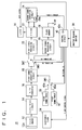
- a digital still camera 10 of this embodiment includes a CCD imager 12.
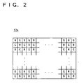
- the CCD imager 12 receives optical images of an object through a mosaic type primary-color filter 12a as shown in Figure 2 to create a camera signal corresponding to the optical image.
- the camera signal is subjected to correlate double sampling and automatic gain control by a CDS/AGC circuit 14.
- the camera signal thus processed is converted into a digital signal by an A/D converter 16.
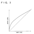
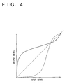
- a third gamma table 30 is previously stored with a gamma characteristic for bit map display, as shown in Figure 4.
- a first gamma correction circuit 18 makes reference the third gamma table to gamma-correct the digital signal from the A/D converter 16 in a manner appropriate for bit map display.
- the gamma-corrected digital signal, or a first image signal is delivered to a first signal processing circuit 20 where it is subjected to processing appropriate for LCD display by an interpolation/thinning-out circuit 20a and an image processing circuit 20b shown in Figure 6.
- the number of pixels of an LCD 36 is 1/4 of the number of pixels of the CCD imager 12, and the digital signal contains image pixel signals each having either one component of R, G or B so that the pixel signal is interpolated with the every other adjacent pixel every two pixels in the respective horizontal and vertical directions.
- the pixel signal thus interpolated only is delivered to a VRAM 22.
- four pixels to be considered contain components of G 1 , G 2 , R and B.
- the adjacent R and B components are used as they are while the G component is determined according to Equation 1.
- G (G 1 + G 2 )/2
- the number of pixels of the LCD 36 is 1/4 of the number of pixels of the CCD imager 12 as stated above, so that there is no necessity of interpolation processing for a pixel of R, B or G 2 component.
- the component G 1 may be outputted as it is without determining the component G according to Equation 1.
- the output of the interpolation/thinning-out circuit 20a is subsequently subjected to image processing such as color separation by the image processing circuit 20b.
- image processing such as color separation by the image processing circuit 20b.
- the second image signal thus obtained is successively written into the VRAM 22.
- the shutter release button 38 is not depressed, the second gamma-correction circuit 24 is disabled so that the second image signal stored in the VRAM 22 is delivered to the LCD 32 as it is, thereby displaying a desired image-quality motion picture.
- the control circuit 42 turns on the switch SW3 in addition to the switch SW2, to connect the switch SW1 to a terminal 40a, activating a second gamma correction circuit 24a.
- the control circuit 42 further causes radiation in an electronic flash 34.
- the first gamma table 32 is previously stored with a gamma characteristic for raster scan display as shown in Figure 3.
- the first gamma correction circuit 18 makes reference to the first gamma table to make correction to the camera signal from the A/D converter 16 appropriately for raster scan display.
- the switch SW1 also returns on, so that the first image signal outputted from the first gamma correction circuit 18 is delivered also to the second signal processing circuit 26.
- the control circuit 42 turns off the switches SW2 and SW3 at a time when the first gamma correction circuit 18 creates a first image signal by one frame after the shutter release button 38 was depressed. This disables the CCD imager 12, the CDS/AGC circuit 14 and the A/D converter 16 so that the first signal processing circuit 20 and the second signal processing circuit 26 are inputted only with a still image signal upon depression of the shutter release button 38.
- the interpolation circuit 26a creates R, G and B components for one pixel from 16 pixel signals.
- the signals R, G and B thus created are converted into Y, U and V signals, and thereafter the Y, U and V signals are compressed by a JPEG compression circuit 26c according to a JPEG format.
- the compressed signals are stored in the flash memory 28.
- the detailed operation of the interpolation circuit 26a is described in Japanese Provisional Patent Publication No. H8-237672 [H04N9/07] that has been laid open on September 13, 1996.
- the image stored in the flash memory 28 is outputted as required to a personal computer or a television receiver not shown so that the image picture is displayed on a CRT.
- the first image signal via the switch SW2 is subjected to interpolation/thinning-out and image processing by the first signal processing circuit 20 in a manner similar to the above so that a thinned-out signal having a characteristic appropriate for raster scan display is stored in the VRAM 22.
- the second gamma correction circuit 24 is in activation so that the thinned-out signal is subjected to gamma correction. That is, the second gamma correction circuit 24 is previously stored with the second gamma table 24 having a gamma characteristic, as shown in Figure 5 for, converting a raster-scan display gamma characteristic into a dot-matrix display gamma characteristic.
- the second gamma-correction circuit 24 read by one pixel of a thinned-out image signal out of the VRAM 22, to make gamma correction to each pixel signal according to the second gamma table. This provides a thinned-out image signal suited for bit map display, and the thinned-out image signal is delivered to the LCD 36. To this end, on the LCD 36 is displayed a high-quality still picture at a time when the shutter release button 38 has been depressed.
- the gamma characteristic of the second gamma table 20a is of a characteristic that is synthesized of a reverse gamma characteristic to the gamma characteristic of the gamma first table 32 with a gamma characteristic of the third gamma table 30. It takes time from the depression of the shutter release button 38 to the completion of gamma correction by the second gamma correction circuit 24, so that in that duration the control circuit 42 carries out muting to the LCD 36.
- the LCD 36 while being muted cuts-off an input from the VRAM 22 to output a predetermined black level signal. This provides display of a black image on the LCD 36 while the gamma correction is being made, preventing outputting of unwanted still image pictures.
- the control circuit 42 brings the operation back to the state that the shutter release button 38 is before depressed thereby displaying a motion picture on the LCD 36.
- the time period required for interpolation/thinning-out and image processing by the first signal processing circuit 20 and the gamma correction by the second gamma correction circuit 24 is shorter than that of the interpolation, YUV conversion and compression processing by the second signal processing circuit 26. Consequently, there is no case that the LCD 36 displays a motion picture without through the display of a still picture after the cancellation of muting.
- the digital still camera 10 By the operation of the digital still camera 10 in this manner, it is possible to display on the LCD 36 a high-quality still picture at the time that the shutter release button 38 is depressed. That is, where an object moving at a high speed is photographed, there is no possibility of occurring deviation between a still picture recorded by the flash memory 28 and a still picture displayed on the LCD 36. Also, since the first image signal is corrected by the first gamma table and thereafter the thinned-out image signal is corrected again by the use of the second gamma table 24a, both of the still picture displayed on the LCD 36 and the still picture recorded by the flash memory 28 have a proper image quality.
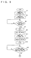
- the control circuit 42 upon turning on a power supply, starts processing as shown by the flowchart in Figures 9 and 10. That is, at a step S1 the switch SW1 is connected to the terminal 40a, and then, at a step S3 the switch SW2 is turned on and the switch SW3 is turned off. Subsequently, it is determined at a step S5 whether or not the shutter release button 38 is depressed. Here, if "NO", the LCD 36 continues to display the moving picture.
- the first gamma correction circuit 18 makes reference to the third gamma table 30 to gamma-correct the first image signal, and the VRAM 22 holds a thinned-out image signal with an image quality suited for bit map display, so that the LCD 36 displays a high quality moving picture.
- the control circuit 42 determines "YES" at a step S5, and outputs a muting signal at a step S7 to subject muting to the LCD 36. Then, at a step S9 a predetermined time period of from the depression of the shutter release button 38 up to the completion of the gamma-correction by the second gamma correction circuit 24, is set to a timer 42a, starting time counting.
- the control circuit 42 subsequently connects the switch SW1 to the terminal 40a at a step S11, turns on both the switches SW2 and SW3, at a step S13, and causes radiation by the electronic flash 34 at a step S15. This makes gamma-correction to the camera signal outputted from the A/D converter 16 according to the first gamma table.
- the control circuit 42 determines "YES" at a step S17, to turn off the switch SW2 and SW3 at a step S19. Consequently, there are thereafter no cases that the first signal processing circuit 20 and the second signal processing circuit 26 are inputted with the first image signal, so that the thinned-out image signal of the still picture is stored by the VRAM that is at the time that the shutter release button 38 is depressed.
- the control circuit 42 activates the second gamma-correction circuit 24 at a step S21. This makes gamma-correction to the thinned-out image signal stored by the VRAM 22.
- the control circuit 42 makes reference to the timer 42a at a step S23 to determine whether or not the predetermined time period has been elapsed. If "YES", it is determined that the second gamma-correction circuit 24 has completed correction, canceling the muting at a step S25.
- the second gamma-correction circuit 24 is disabled, and at a step S29 it is determined whether the storage of the compressed signal onto the flash memory 28 is completed or not.
- the process returns to the step S1, repeating the similar process to the above. That is, the control circuit 42 causes the switch SW1 to be connected to the first gamma table side during the time period of from the depression of the shutter release button 38 up to the completion of recording the compressed signal, while it causes the switch SW1 to be connected to the second gamma table side before depression of the shutter release button 38 or after completion of record operation. Therefore, in response to the completion of recording to the flash memory 28, the content of display on the LCD 36 is changed over from the still picture to a motion picture.
- the muting operation may be released at a time that a further routine (not shown) has been executed for a predetermined number of times by supervising the further routine which is started at a time that the shutter release button 38 is depressed.
Abstract
Description
- This invention relates to digital still cameras, more particularly to a digital still camera adapted to display a photographed image picture on an LCD and store the same picture in a flash memory.
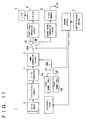
- In a
digital still camera 1 of this kind as shown in Figure 11, the switches SW4 and SW5 are respectively connected to the terminals S1 and S3 while ashutter release button 2 is not depressed. Accordingly, a gamma-correction circuit 3 makes reference to a second gamma table to gamma-correct a motion image signal appropriate for bit map display, thereby outputting a high-quality motion picture on anL CD 5. On the other hand, if theshutter release button 2 is depressed, the switch SW4 is connected to the terminal S2 while the switch SW5 is connected to a terminal S4. When a still image upon depression of theshutter release button 2 is obtained from the gamma-correction circuit, the switch SW4 is connected to the terminal S5, thereby disabling theCCD imager 6. The gamma-correction circuit 3 makes reference to a first gamma table 4a to gamma-correct a still image signal from an A/D converter 7 appropriately for raster scan display so that a still image signal after correction is stored in theflash memory 8. On the other hand, aVRAM 9 is stored with an image signal that is immediately before changing over of the switch SW4 so that the image signal is displayed on theLCD 5 for a predetermined time period until the storage to the flash memory such has been completed. - However, in such a conventional art, there is difference in time between the image picture displayed on the
LCD 5 and the picture image stored in theflash memory 8. As a result, there arises deviation between the images if an object is moving at a high speed. - It is therefore a primary object of the invention to provide a novel digital still camera.
- Another object of the invention relates to a digital still camera which is capable of displaying a still image picture with high quality at time when a shutter release button is depressed.
- In accordance with the invention, a digital still camera comprising: a shutter release button; a first correction means for correcting a camera signal, at time that said shutter release button is depressed, by a first gamma characteristic to output a first image signal; a storing means for storing the first image signal in a memory; a second correction means for correcting the first image signal by a second gamma characteristic to output a second image signal; and a display means for displaying the second image signal until storage of the first image signal to said memory is completed.
- In the present invention, when the shutter release button is depressed, the camera signal at that time is corrected by the gamma characteristic of the raster scan display. A first image signal obtained is subjected for example to interpolation, YUV conversion and JPEG compression so that the compressed signal is stored for example in a flash memory. The first image signal is also subjected for example to image processing such as interpolation/thinning-out and color separation, and the thinned-out image signal is corrected by a gamma characteristic for changing a raster-scan display gamma characteristic into a dot-matrix display gamma characteristic. A second image signal obtained by the correction is displayed on a dot-matrix display.
- In accordance with one aspect of the invention, the first correcting means includes a first table having a gamma characteristic of a raster scan display, a third table having a gamma characteristic of a dot matrix display, and a switch for selecting either one of the first table or the third table. While the shutter release button is not depressed, the switch is connected to a third-table side and the second correcting means is disabled. This provides display on the dot matrix display an image that is gamma-corrected appropriately for dot matrix displaying. If the shutter release button is depressed, the switch is connected to a first-table side and the second correcting means is enabled. Accordingly, the camera signal is first corrected by a first gamma correcting means so as to be suited for the raster scan display, and thereafter the thinned-out image signal is corrected so as to be suited for the bit matrix display. To this end, display is made on the dot matrix display for a desired still image picture at the time of depressing the shutter release button.
- In accordance with another aspect of the invention, a muting means subjects muting to the display means during a second predetermined period from depression of said shutter release button to completion of correction by the second correcting means. Therefore, there is no possibility of displaying an unwanted image picture on the dot matrix display.
- In another aspect of the invention, an electronic flash for example is radiated in response to operation of the shutter release button so that a still image at that time is displayed on the dot matrix display and stored in a flash memory.
- According to the invention, the camera signal at a time that the shutter release button is depressed is corrected by the first gamma characteristic and the first image signal is corrected by the second gamma characteristic, so that it is possible to display a high-quality still image picture that is taken at the time of depression of the shutter release button.
- The above described objects and other objects, features, aspects and advantages of the present invention will become more apparent from the following detailed description of the present invention when taken in conjunction with the accompanying drawings.
-
- Figure 1 is a block diagram showing one embodiment of this invention;
- Figure 2 is an illustrative view showing a mosaic type primary-color filter;
- Figure 3 is a graph showing a gamma characteristic of raster scan display;
- Figure 4 is a graph showing a gamma characteristic of dot matrix display;
- Figure 5 is a graph showing a gamma characteristic for conversion of a raster-scan display gamma characteristic into a dot-matrix display gamma characteristic;
- Figure 6 is a block diagram showing a first signal processing circuit;
- Figure 7 is an illustrative view showing interpolation and thinning-out processes;
- Figure 8 is a block diagram showing a second signal processing circuit;
- Figure 9 is a flowchart showing operational positions in Figure 1 embodiment;
- Figure 10 is a flowchart showing another positions of Figure 1 embodiment.
- Figure 11 is a block diagram showing a conventional art.
- Referring to Figure 1, a digital
still camera 10 of this embodiment includes aCCD imager 12. TheCCD imager 12 receives optical images of an object through a mosaic type primary-color filter 12a as shown in Figure 2 to create a camera signal corresponding to the optical image. The camera signal is subjected to correlate double sampling and automatic gain control by a CDS/AGC circuit 14. The camera signal thus processed is converted into a digital signal by an A/D converter 16. - While a
shutter release button 38 is not depressed, acontrol circuit 42 connects the switch SW1 to aterminal 40b, turned on a switch SW2, and turned off a switch SW3. A third gamma table 30 is previously stored with a gamma characteristic for bit map display, as shown in Figure 4. A firstgamma correction circuit 18 makes reference the third gamma table to gamma-correct the digital signal from the A/D converter 16 in a manner appropriate for bit map display. The gamma-corrected digital signal, or a first image signal, is delivered to a firstsignal processing circuit 20 where it is subjected to processing appropriate for LCD display by an interpolation/thinning-outcircuit 20a and animage processing circuit 20b shown in Figure 6. - That is, the number of pixels of an
LCD 36 is 1/4 of the number of pixels of theCCD imager 12, and the digital signal contains image pixel signals each having either one component of R, G or B so that the pixel signal is interpolated with the every other adjacent pixel every two pixels in the respective horizontal and vertical directions. The pixel signal thus interpolated only is delivered to aVRAM 22. Explaining in detail by using Figure 7, four pixels to be considered contain components of G1, G2, R and B. Where generating R, G and B components at a position of a pixel with a G1 component, the adjacent R and B components are used as they are while the G component is determined according toEquation 1.
- Incidentally, the number of pixels of the
LCD 36 is 1/4 of the number of pixels of theCCD imager 12 as stated above, so that there is no necessity of interpolation processing for a pixel of R, B or G2 component. Incidentally, the component G1 may be outputted as it is without determining the component G according toEquation 1. - The output of the interpolation/thinning-out
circuit 20a is subsequently subjected to image processing such as color separation by theimage processing circuit 20b. The second image signal thus obtained is successively written into theVRAM 22. While theshutter release button 38 is not depressed, the second gamma-correction circuit 24 is disabled so that the second image signal stored in theVRAM 22 is delivered to theLCD 32 as it is, thereby displaying a desired image-quality motion picture. - On the other hand, when the
shutter release button 38 is depressed, thecontrol circuit 42 turns on the switch SW3 in addition to the switch SW2, to connect the switch SW1 to aterminal 40a, activating a secondgamma correction circuit 24a. Thecontrol circuit 42 further causes radiation in anelectronic flash 34. The first gamma table 32 is previously stored with a gamma characteristic for raster scan display as shown in Figure 3. The firstgamma correction circuit 18 makes reference to the first gamma table to make correction to the camera signal from the A/D converter 16 appropriately for raster scan display. When theshutter release button 38 is depressed, the switch SW1 also returns on, so that the first image signal outputted from the firstgamma correction circuit 18 is delivered also to the secondsignal processing circuit 26. Thecontrol circuit 42 turns off the switches SW2 and SW3 at a time when the firstgamma correction circuit 18 creates a first image signal by one frame after theshutter release button 38 was depressed. This disables theCCD imager 12, the CDS/AGC circuit 14 and the A/D converter 16 so that the firstsignal processing circuit 20 and the secondsignal processing circuit 26 are inputted only with a still image signal upon depression of theshutter release button 38. - Referring to Figure 8, in the second
signal processing circuit 26, theinterpolation circuit 26a creates R, G and B components for one pixel from 16 pixel signals. The signals R, G and B thus created are converted into Y, U and V signals, and thereafter the Y, U and V signals are compressed by aJPEG compression circuit 26c according to a JPEG format. The compressed signals are stored in theflash memory 28. Incidentally, the detailed operation of theinterpolation circuit 26a is described in Japanese Provisional Patent Publication No. H8-237672 [H04N9/07] that has been laid open on September 13, 1996. The image stored in theflash memory 28 is outputted as required to a personal computer or a television receiver not shown so that the image picture is displayed on a CRT. - On the other hand, the first image signal via the switch SW2 is subjected to interpolation/thinning-out and image processing by the first
signal processing circuit 20 in a manner similar to the above so that a thinned-out signal having a characteristic appropriate for raster scan display is stored in theVRAM 22. When theshutter release button 38 is depressed, the secondgamma correction circuit 24 is in activation so that the thinned-out signal is subjected to gamma correction. That is, the secondgamma correction circuit 24 is previously stored with the second gamma table 24 having a gamma characteristic, as shown in Figure 5 for, converting a raster-scan display gamma characteristic into a dot-matrix display gamma characteristic. The second gamma-correction circuit 24 read by one pixel of a thinned-out image signal out of theVRAM 22, to make gamma correction to each pixel signal according to the second gamma table. This provides a thinned-out image signal suited for bit map display, and the thinned-out image signal is delivered to theLCD 36. To this end, on theLCD 36 is displayed a high-quality still picture at a time when theshutter release button 38 has been depressed. Incidentally, the gamma characteristic of the second gamma table 20a is of a characteristic that is synthesized of a reverse gamma characteristic to the gamma characteristic of the gamma first table 32 with a gamma characteristic of the third gamma table 30. It takes time from the depression of theshutter release button 38 to the completion of gamma correction by the secondgamma correction circuit 24, so that in that duration thecontrol circuit 42 carries out muting to theLCD 36. TheLCD 36 while being muted cuts-off an input from theVRAM 22 to output a predetermined black level signal. This provides display of a black image on theLCD 36 while the gamma correction is being made, preventing outputting of unwanted still image pictures. After the muting has been canceled, although theLCD 36 displays with a still picture, the display of the still picture ends at the completion of writing the compression signal into theflash memory 28. Thecontrol circuit 42 brings the operation back to the state that theshutter release button 38 is before depressed thereby displaying a motion picture on theLCD 36. - Incidentally, the time period required for interpolation/thinning-out and image processing by the first
signal processing circuit 20 and the gamma correction by the secondgamma correction circuit 24 is shorter than that of the interpolation, YUV conversion and compression processing by the secondsignal processing circuit 26. Consequently, there is no case that theLCD 36 displays a motion picture without through the display of a still picture after the cancellation of muting. - By the operation of the digital
still camera 10 in this manner, it is possible to display on the LCD 36 a high-quality still picture at the time that theshutter release button 38 is depressed. That is, where an object moving at a high speed is photographed, there is no possibility of occurring deviation between a still picture recorded by theflash memory 28 and a still picture displayed on theLCD 36. Also, since the first image signal is corrected by the first gamma table and thereafter the thinned-out image signal is corrected again by the use of the second gamma table 24a, both of the still picture displayed on theLCD 36 and the still picture recorded by theflash memory 28 have a proper image quality. - The
control circuit 42, upon turning on a power supply, starts processing as shown by the flowchart in Figures 9 and 10. That is, at a step S1 the switch SW1 is connected to the terminal 40a, and then, at a step S3 the switch SW2 is turned on and the switch SW3 is turned off. Subsequently, it is determined at a step S5 whether or not theshutter release button 38 is depressed. Here, if "NO", theLCD 36 continues to display the moving picture. That is, the firstgamma correction circuit 18 makes reference to the third gamma table 30 to gamma-correct the first image signal, and theVRAM 22 holds a thinned-out image signal with an image quality suited for bit map display, so that theLCD 36 displays a high quality moving picture. - On the other hand, if the
shutter release button 38 is depressed, thecontrol circuit 42 determines "YES" at a step S5, and outputs a muting signal at a step S7 to subject muting to theLCD 36. Then, at a step S9 a predetermined time period of from the depression of theshutter release button 38 up to the completion of the gamma-correction by the secondgamma correction circuit 24, is set to atimer 42a, starting time counting. Thecontrol circuit 42 subsequently connects the switch SW1 to the terminal 40a at a step S11, turns on both the switches SW2 and SW3, at a step S13, and causes radiation by theelectronic flash 34 at a step S15. This makes gamma-correction to the camera signal outputted from the A/D converter 16 according to the first gamma table. - After the gamma-
correction circuit 18 completes to output the first image signal of one frame, i.e. the still picture signal at the time that theshutter release button 38 is depressed, thecontrol circuit 42 determines "YES" at a step S17, to turn off the switch SW2 and SW3 at a step S19. Consequently, there are thereafter no cases that the firstsignal processing circuit 20 and the secondsignal processing circuit 26 are inputted with the first image signal, so that the thinned-out image signal of the still picture is stored by the VRAM that is at the time that theshutter release button 38 is depressed. - The
control circuit 42 activates the second gamma-correction circuit 24 at a step S21. This makes gamma-correction to the thinned-out image signal stored by theVRAM 22. Thecontrol circuit 42 makes reference to thetimer 42a at a step S23 to determine whether or not the predetermined time period has been elapsed. If "YES", it is determined that the second gamma-correction circuit 24 has completed correction, canceling the muting at a step S25. At a step S27 the second gamma-correction circuit 24 is disabled, and at a step S29 it is determined whether the storage of the compressed signal onto theflash memory 28 is completed or not. If "YES", the process returns to the step S1, repeating the similar process to the above. That is, thecontrol circuit 42 causes the switch SW1 to be connected to the first gamma table side during the time period of from the depression of theshutter release button 38 up to the completion of recording the compressed signal, while it causes the switch SW1 to be connected to the second gamma table side before depression of theshutter release button 38 or after completion of record operation. Therefore, in response to the completion of recording to theflash memory 28, the content of display on theLCD 36 is changed over from the still picture to a motion picture. - In addition, though a time period for the gamma correction by the second
gamma correction circuit 24 is defined by thetimer 42a in this embodiment, the muting operation may be released at a time that a further routine (not shown) has been executed for a predetermined number of times by supervising the further routine which is started at a time that theshutter release button 38 is depressed. - Although the present invention has been described and illustrated in detail, it is clearly understood that the same is by way of illustration and example only and is not to be taken by way of limitation, the spirit and scope of the present invention being limited only by the terms of the appended claims.
Claims (6)
- A digital still camera comprising:a shutter release button;a first correction means for correcting a camera signal, at time that said shutter release button is depressed, by a first gamma characteristic to output a first image signal;a storing means for storing the first image signal in a memory;a second correction means for correcting the first image signal by a second gamma characteristic to output a second image signal; anda display means for displaying the second image signal until storage of the first image signal to said memory is completed.
- A digital still camera according to claim 1, wherein the first correction means includes a first table previously stored with the first gamma characteristic, and said second correction means includes a second table previously stored with the second gamma characteristic.
- A digital still camera according to claim 2, wherein the first correction means further includes a third table previously stored with a third gamma characteristic and a selecting means for selecting either one of the first table or the third table, said camera further comprising:a control means for causing said selecting means to select the first table during a time period of from depression of said shutter release button to completion of storage of the first image signal to said memory, and select the third table before depression of said shutter release button or after completion of storage of the first image signal; anda disabling means for disabling said second correction means while said selecting means selects the third table.
- A digital still camera according to claim 3, wherein said display means is a dot matrix display,
said first gamma characteristic has a gamma characteristic of raster scan display, said third gamma characteristic has a gamma characteristic of the dot matrix display, and the second gamma characteristic has a gamma characteristic for converting the first gamma characteristic into the third gamma characteristic. - A digital still camera according to claim 1, further comprising:a muting means for subjecting muting to said display means during a second predetermined period from depression of said shutter release button to completion of correction by said second correcting means.
- A digital still camera according to claim 1, further comprising:an electronic flash means that operates in response to operation of said shutter release button.
Applications Claiming Priority (3)
| Application Number | Priority Date | Filing Date | Title |
|---|---|---|---|
| JP13922296A JP3208324B2 (en) | 1996-05-31 | 1996-05-31 | Digital still camera |
| JP13922296 | 1996-05-31 | ||
| JP139222/96 | 1996-05-31 |
Publications (2)
| Publication Number | Publication Date |
|---|---|
| EP0810778A2 true EP0810778A2 (en) | 1997-12-03 |
| EP0810778A3 EP0810778A3 (en) | 2001-03-14 |
Family
ID=15240355
Family Applications (1)
| Application Number | Title | Priority Date | Filing Date |
|---|---|---|---|
| EP97108812A Withdrawn EP0810778A3 (en) | 1996-05-31 | 1997-06-02 | Digital still camera with a gamma correction circuit |
Country Status (4)
| Country | Link |
|---|---|
| US (1) | US5990949A (en) |
| EP (1) | EP0810778A3 (en) |
| JP (1) | JP3208324B2 (en) |
| CN (1) | CN1096178C (en) |
Cited By (7)
| Publication number | Priority date | Publication date | Assignee | Title |
|---|---|---|---|---|
| EP0952729A2 (en) * | 1998-04-20 | 1999-10-27 | Casio Computer Co., Ltd. | Electronic camera apparatus equipped with preview image preparation function |
| WO2000021303A1 (en) * | 1998-10-06 | 2000-04-13 | Matsushita Electric Industrial Co., Ltd. | η CORRECTION CIRCUIT AND η CORRECTION METHOD |
| WO2000030338A2 (en) * | 1998-11-13 | 2000-05-25 | Silicon Film Technologies, Inc. | Electronic film system and method of film processing |
| EP1028595A2 (en) * | 1999-02-10 | 2000-08-16 | Texas Instruments Incorporated | Improvements in or relating to digital cameras |
| US6356276B1 (en) | 1998-03-18 | 2002-03-12 | Intel Corporation | Median computation-based integrated color interpolation and color space conversion methodology from 8-bit bayer pattern RGB color space to 12-bit YCrCb color space |
| US6392699B1 (en) * | 1998-03-04 | 2002-05-21 | Intel Corporation | Integrated color interpolation and color space conversion algorithm from 8-bit bayer pattern RGB color space to 12-bit YCrCb color space |
| EP1848199A1 (en) * | 2006-04-20 | 2007-10-24 | Sony Corporation | Imaging apparatus and method of processing image signal |
Families Citing this family (16)
| Publication number | Priority date | Publication date | Assignee | Title |
|---|---|---|---|---|
| JPH10276349A (en) * | 1997-03-27 | 1998-10-13 | Asahi Optical Co Ltd | Image signal correction device |
| US7057653B1 (en) * | 1997-06-19 | 2006-06-06 | Minolta Co., Ltd. | Apparatus capable of image capturing |
| KR20000026234A (en) * | 1998-10-19 | 2000-05-15 | 유무성 | Video presenter |
| JP3877474B2 (en) * | 1999-08-03 | 2007-02-07 | 三洋電機株式会社 | Electronic camera |
| JP3902525B2 (en) * | 2002-09-05 | 2007-04-11 | 三洋電機株式会社 | Image signal processing device |
| EP1482724B1 (en) * | 2003-05-19 | 2007-07-11 | STMicroelectronics S.A. | Image processing method for digital images with exposure correction by recognition of skin areas of the subject. |
| KR100744050B1 (en) * | 2003-11-28 | 2007-07-30 | 삼성전자주식회사 | Image scanning device converting analog signal into digital signal corresponding with operating mode and a method thereof |
| KR100758295B1 (en) * | 2005-01-25 | 2007-09-12 | 삼성전자주식회사 | Gamma correction device and display apparatus including the same and method for gamma correction thereof |
| JP4500711B2 (en) * | 2005-03-10 | 2010-07-14 | キヤノン株式会社 | Camera integrated recording and playback device |
| US7589779B2 (en) * | 2005-04-13 | 2009-09-15 | Seiko Epson Corporation | Imaging module, interface, and method handling multiple simultaneous data types |
| TWI264940B (en) * | 2005-06-29 | 2006-10-21 | Quanta Comp Inc | Method and apparatus for nonlinear coding with 1st order power functions in digital imaging system |
| CN101193314B (en) * | 2006-11-30 | 2012-06-27 | 北京思比科微电子技术有限公司 | Image processing device and method for image sensor |
| JP2008219317A (en) * | 2007-03-02 | 2008-09-18 | Sharp Corp | Imaging apparatus |
| US7986356B2 (en) * | 2007-07-25 | 2011-07-26 | Hewlett-Packard Development Company, L.P. | System and method for determining a gamma curve of a display device |
| US20090027504A1 (en) * | 2007-07-25 | 2009-01-29 | Suk Hwan Lim | System and method for calibrating a camera |
| JP6250970B2 (en) * | 2013-07-30 | 2017-12-20 | キヤノン株式会社 | Image processing apparatus, imaging apparatus, image processing method, program, and recording medium |
Citations (4)
| Publication number | Priority date | Publication date | Assignee | Title |
|---|---|---|---|---|
| US4394688A (en) * | 1981-08-25 | 1983-07-19 | Hamamatsu Systems, Inc. | Video system having an adjustable digital gamma correction for contrast enhancement |
| JPS63232682A (en) * | 1987-03-20 | 1988-09-28 | Canon Inc | Video signal transmitting/receiving system |
| JPH04316282A (en) * | 1991-04-16 | 1992-11-06 | Fuji Photo Film Co Ltd | Picture memory device and its operation |
| EP0708433A2 (en) * | 1994-10-20 | 1996-04-24 | Canon Kabushiki Kaisha | Display control apparatus and method |
Family Cites Families (3)
| Publication number | Priority date | Publication date | Assignee | Title |
|---|---|---|---|---|
| EP0374285A1 (en) * | 1988-12-21 | 1990-06-27 | Deutsche ITT Industries GmbH | Portable electronic image pick-up device |
| US5764287A (en) * | 1992-08-31 | 1998-06-09 | Canon Kabushiki Kaisha | Image pickup apparatus with automatic selection of gamma correction valve |
| JP3438205B2 (en) * | 1993-02-25 | 2003-08-18 | 株式会社リコー | Digital electronic camera device |
-
1996
- 1996-05-31 JP JP13922296A patent/JP3208324B2/en not_active Expired - Fee Related
-
1997
- 1997-05-27 US US08/863,975 patent/US5990949A/en not_active Expired - Fee Related
- 1997-05-31 CN CN97105412A patent/CN1096178C/en not_active Expired - Fee Related
- 1997-06-02 EP EP97108812A patent/EP0810778A3/en not_active Withdrawn
Patent Citations (4)
| Publication number | Priority date | Publication date | Assignee | Title |
|---|---|---|---|---|
| US4394688A (en) * | 1981-08-25 | 1983-07-19 | Hamamatsu Systems, Inc. | Video system having an adjustable digital gamma correction for contrast enhancement |
| JPS63232682A (en) * | 1987-03-20 | 1988-09-28 | Canon Inc | Video signal transmitting/receiving system |
| JPH04316282A (en) * | 1991-04-16 | 1992-11-06 | Fuji Photo Film Co Ltd | Picture memory device and its operation |
| EP0708433A2 (en) * | 1994-10-20 | 1996-04-24 | Canon Kabushiki Kaisha | Display control apparatus and method |
Non-Patent Citations (2)
| Title |
|---|
| PATENT ABSTRACTS OF JAPAN vol. 013, no. 034 (E-708), 25 January 1989 (1989-01-25) & JP 63 232682 A (CANON INC), 28 September 1988 (1988-09-28) * |
| PATENT ABSTRACTS OF JAPAN vol. 017, no. 150 (E-1339), 25 March 1993 (1993-03-25) & JP 04 316282 A (FUJI PHOTO FILM CO LTD), 6 November 1992 (1992-11-06) & US 5 589 889 A (KAWAOKA) 31 December 1996 (1996-12-31) * |
Cited By (13)
| Publication number | Priority date | Publication date | Assignee | Title |
|---|---|---|---|---|
| US6392699B1 (en) * | 1998-03-04 | 2002-05-21 | Intel Corporation | Integrated color interpolation and color space conversion algorithm from 8-bit bayer pattern RGB color space to 12-bit YCrCb color space |
| US6356276B1 (en) | 1998-03-18 | 2002-03-12 | Intel Corporation | Median computation-based integrated color interpolation and color space conversion methodology from 8-bit bayer pattern RGB color space to 12-bit YCrCb color space |
| EP0952729A2 (en) * | 1998-04-20 | 1999-10-27 | Casio Computer Co., Ltd. | Electronic camera apparatus equipped with preview image preparation function |
| EP0952729A3 (en) * | 1998-04-20 | 2002-01-23 | Casio Computer Co., Ltd. | Electronic camera apparatus equipped with preview image preparation function |
| US6340996B1 (en) | 1998-10-06 | 2002-01-22 | Matsushita Electric Industrial Co., Ltd. | γ Correction system and method utilizing graph approximation |
| AU739565B2 (en) * | 1998-10-06 | 2001-10-18 | Matsushita Electric Industrial Co., Ltd. | Gamma correction circuit and gamma correction method |
| WO2000021303A1 (en) * | 1998-10-06 | 2000-04-13 | Matsushita Electric Industrial Co., Ltd. | η CORRECTION CIRCUIT AND η CORRECTION METHOD |
| WO2000030338A3 (en) * | 1998-11-13 | 2000-08-24 | Silicon Film Technologies Inc | Electronic film system and method of film processing |
| WO2000030338A2 (en) * | 1998-11-13 | 2000-05-25 | Silicon Film Technologies, Inc. | Electronic film system and method of film processing |
| EP1028595A2 (en) * | 1999-02-10 | 2000-08-16 | Texas Instruments Incorporated | Improvements in or relating to digital cameras |
| EP1028595A3 (en) * | 1999-02-10 | 2002-07-17 | Texas Instruments Incorporated | Improvements in or relating to digital cameras |
| EP1848199A1 (en) * | 2006-04-20 | 2007-10-24 | Sony Corporation | Imaging apparatus and method of processing image signal |
| US7760243B2 (en) | 2006-04-20 | 2010-07-20 | Sony Corporation | Imaging apparatus and method of processing image signal |
Also Published As
| Publication number | Publication date |
|---|---|
| JP3208324B2 (en) | 2001-09-10 |
| JPH09322017A (en) | 1997-12-12 |
| EP0810778A3 (en) | 2001-03-14 |
| US5990949A (en) | 1999-11-23 |
| CN1170148A (en) | 1998-01-14 |
| CN1096178C (en) | 2002-12-11 |
Similar Documents
| Publication | Publication Date | Title |
|---|---|---|
| US5990949A (en) | Digital still camera which displays a gamma-corrected high-quality still image upon depression of a shutter release button but without displaying an unwanted image | |
| US7733388B2 (en) | Digital camera capable of image processing for display on a monitor | |
| US4903132A (en) | Electronic still camera with slow-in, fast out memory addressing | |
| US6542192B2 (en) | Image display method and digital still camera providing rapid image display by displaying low resolution image followed by high resolution image | |
| KR100541301B1 (en) | Digital camera | |
| US5497194A (en) | Electronic camera for photographing and recording an image and for recording and reproducing a voice | |
| US6466263B1 (en) | Electronic still camera having pointing indicator showing operation mode | |
| US20030081954A1 (en) | Digital camera | |
| US20050099518A1 (en) | Image reproduction apparatus and image capturing apparatus | |
| US5874999A (en) | Image processing apparatus with multiple data modes | |
| US20080118220A1 (en) | Method of capturing still image during reproduction of moving picture | |
| JP4829391B2 (en) | Imaging device | |
| JP2007174160A (en) | Imaging apparatus | |
| EP0952729A2 (en) | Electronic camera apparatus equipped with preview image preparation function | |
| JPH11187351A (en) | Image pickup device and its control method | |
| JP2001169152A (en) | Electronic camera, method for display state adjustment of electronic camera, and recording medium | |
| JP3253536B2 (en) | Electronic still camera | |
| JP2003087647A (en) | Digital still camera | |
| JP3229144B2 (en) | Digital still image data recording apparatus and recording method thereof | |
| JP2001268435A (en) | Image processing method, recording medium for image processing and image processor | |
| JP4019162B2 (en) | Digital camera | |
| JP3523398B2 (en) | Digital still video camera | |
| JPH10341361A (en) | Digital camera with panoramic image-photographing function | |
| JPH06315106A (en) | Image handling device | |
| JP2007221237A (en) | Camera |
Legal Events
| Date | Code | Title | Description |
|---|---|---|---|
| PUAI | Public reference made under article 153(3) epc to a published international application that has entered the european phase |
Free format text: ORIGINAL CODE: 0009012 |
|
| AK | Designated contracting states |
Kind code of ref document: A2 Designated state(s): DE FR GB |
|
| PUAL | Search report despatched |
Free format text: ORIGINAL CODE: 0009013 |
|
| AK | Designated contracting states |
Kind code of ref document: A3 Designated state(s): AT BE CH DE DK ES FI FR GB GR IE IT LI LU MC NL PT SE |
|
| 17P | Request for examination filed |
Effective date: 20010417 |
|
| AKX | Designation fees paid |
Free format text: DE FR GB |
|
| STAA | Information on the status of an ep patent application or granted ep patent |
Free format text: STATUS: THE APPLICATION HAS BEEN WITHDRAWN |
|
| 18W | Application withdrawn |
Effective date: 20040603 |