EP0807846A2 - Color Display and its manufacturing method - Google Patents
Color Display and its manufacturing method Download PDFInfo
- Publication number
- EP0807846A2 EP0807846A2 EP97303293A EP97303293A EP0807846A2 EP 0807846 A2 EP0807846 A2 EP 0807846A2 EP 97303293 A EP97303293 A EP 97303293A EP 97303293 A EP97303293 A EP 97303293A EP 0807846 A2 EP0807846 A2 EP 0807846A2
- Authority
- EP
- European Patent Office
- Prior art keywords
- film
- color filter
- color
- black matrix
- forming
- Prior art date
- Legal status (The legal status is an assumption and is not a legal conclusion. Google has not performed a legal analysis and makes no representation as to the accuracy of the status listed.)
- Withdrawn
Links
- 238000004519 manufacturing process Methods 0.000 title claims abstract description 19
- XLOMVQKBTHCTTD-UHFFFAOYSA-N Zinc monoxide Chemical compound [Zn]=O XLOMVQKBTHCTTD-UHFFFAOYSA-N 0.000 claims abstract description 178
- 239000011159 matrix material Substances 0.000 claims abstract description 132
- 238000000034 method Methods 0.000 claims abstract description 98
- 239000011787 zinc oxide Substances 0.000 claims abstract description 88
- 239000000758 substrate Substances 0.000 claims abstract description 80
- RYGMFSIKBFXOCR-UHFFFAOYSA-N Copper Chemical compound [Cu] RYGMFSIKBFXOCR-UHFFFAOYSA-N 0.000 claims abstract description 64
- 229910052802 copper Inorganic materials 0.000 claims abstract description 64
- 239000010949 copper Substances 0.000 claims abstract description 64
- 230000008569 process Effects 0.000 claims abstract description 17
- 238000007747 plating Methods 0.000 claims abstract description 15
- 239000010408 film Substances 0.000 claims description 162
- 239000011521 glass Substances 0.000 claims description 74
- 239000010409 thin film Substances 0.000 claims description 37
- 238000009713 electroplating Methods 0.000 claims description 36
- 229920002120 photoresistant polymer Polymers 0.000 claims description 27
- 125000006850 spacer group Chemical group 0.000 claims description 26
- 238000000151 deposition Methods 0.000 claims description 16
- 239000000126 substance Substances 0.000 claims description 15
- QPLDLSVMHZLSFG-UHFFFAOYSA-N Copper oxide Chemical compound [Cu]=O QPLDLSVMHZLSFG-UHFFFAOYSA-N 0.000 claims description 14
- 229910052782 aluminium Inorganic materials 0.000 claims description 14
- XAGFODPZIPBFFR-UHFFFAOYSA-N aluminium Chemical compound [Al] XAGFODPZIPBFFR-UHFFFAOYSA-N 0.000 claims description 14
- 238000000576 coating method Methods 0.000 claims description 13
- 239000005751 Copper oxide Substances 0.000 claims description 12
- 229910000431 copper oxide Inorganic materials 0.000 claims description 12
- 238000003754 machining Methods 0.000 claims description 12
- PIBWKRNGBLPSSY-UHFFFAOYSA-L palladium(II) chloride Chemical compound Cl[Pd]Cl PIBWKRNGBLPSSY-UHFFFAOYSA-L 0.000 claims description 11
- 239000000049 pigment Substances 0.000 claims description 10
- 239000011248 coating agent Substances 0.000 claims description 9
- 239000003086 colorant Substances 0.000 claims description 9
- 230000010287 polarization Effects 0.000 claims description 9
- 238000007772 electroless plating Methods 0.000 claims description 8
- 238000005868 electrolysis reaction Methods 0.000 claims description 6
- 230000001590 oxidative effect Effects 0.000 claims description 6
- 230000003197 catalytic effect Effects 0.000 claims description 5
- 229920006267 polyester film Polymers 0.000 claims description 5
- CDBYLPFSWZWCQE-UHFFFAOYSA-L Sodium Carbonate Chemical compound [Na+].[Na+].[O-]C([O-])=O CDBYLPFSWZWCQE-UHFFFAOYSA-L 0.000 claims description 4
- 230000003449 preventive effect Effects 0.000 claims description 4
- 229910000679 solder Inorganic materials 0.000 claims description 3
- 238000002310 reflectometry Methods 0.000 abstract description 21
- 230000003287 optical effect Effects 0.000 abstract description 10
- 239000000243 solution Substances 0.000 description 21
- 239000004973 liquid crystal related substance Substances 0.000 description 15
- 238000010276 construction Methods 0.000 description 11
- 238000004544 sputter deposition Methods 0.000 description 10
- 229910052751 metal Inorganic materials 0.000 description 9
- 239000002184 metal Substances 0.000 description 9
- 239000000203 mixture Substances 0.000 description 8
- 210000004027 cell Anatomy 0.000 description 7
- 230000008021 deposition Effects 0.000 description 7
- 239000006185 dispersion Substances 0.000 description 7
- 238000000608 laser ablation Methods 0.000 description 7
- 239000002245 particle Substances 0.000 description 7
- MHAJPDPJQMAIIY-UHFFFAOYSA-N Hydrogen peroxide Chemical compound OO MHAJPDPJQMAIIY-UHFFFAOYSA-N 0.000 description 6
- 239000003574 free electron Substances 0.000 description 6
- 239000000463 material Substances 0.000 description 6
- ONDPHDOFVYQSGI-UHFFFAOYSA-N zinc nitrate Chemical compound [Zn+2].[O-][N+]([O-])=O.[O-][N+]([O-])=O ONDPHDOFVYQSGI-UHFFFAOYSA-N 0.000 description 6
- VYZAMTAEIAYCRO-UHFFFAOYSA-N Chromium Chemical compound [Cr] VYZAMTAEIAYCRO-UHFFFAOYSA-N 0.000 description 5
- VYPSYNLAJGMNEJ-UHFFFAOYSA-N Silicium dioxide Chemical compound O=[Si]=O VYPSYNLAJGMNEJ-UHFFFAOYSA-N 0.000 description 5
- 238000002679 ablation Methods 0.000 description 5
- 239000007864 aqueous solution Substances 0.000 description 5
- 229910052804 chromium Inorganic materials 0.000 description 5
- 239000011651 chromium Substances 0.000 description 5
- 239000007788 liquid Substances 0.000 description 5
- KDLHZDBZIXYQEI-UHFFFAOYSA-N palladium Substances [Pd] KDLHZDBZIXYQEI-UHFFFAOYSA-N 0.000 description 5
- 239000004065 semiconductor Substances 0.000 description 5
- 239000011701 zinc Substances 0.000 description 5
- GRYLNZFGIOXLOG-UHFFFAOYSA-N Nitric acid Chemical compound O[N+]([O-])=O GRYLNZFGIOXLOG-UHFFFAOYSA-N 0.000 description 4
- 230000015572 biosynthetic process Effects 0.000 description 4
- 238000004043 dyeing Methods 0.000 description 4
- 230000005672 electromagnetic field Effects 0.000 description 4
- 150000002500 ions Chemical class 0.000 description 4
- 229910017604 nitric acid Inorganic materials 0.000 description 4
- 230000003647 oxidation Effects 0.000 description 4
- 238000007254 oxidation reaction Methods 0.000 description 4
- 238000007639 printing Methods 0.000 description 4
- 230000001681 protective effect Effects 0.000 description 4
- 238000004528 spin coating Methods 0.000 description 4
- YPTUAQWMBNZZRN-UHFFFAOYSA-N dimethylaminoboron Chemical compound [B]N(C)C YPTUAQWMBNZZRN-UHFFFAOYSA-N 0.000 description 3
- XLYOFNOQVPJJNP-UHFFFAOYSA-N water Substances O XLYOFNOQVPJJNP-UHFFFAOYSA-N 0.000 description 3
- 206010034972 Photosensitivity reaction Diseases 0.000 description 2
- QVGXLLKOCUKJST-UHFFFAOYSA-N atomic oxygen Chemical compound [O] QVGXLLKOCUKJST-UHFFFAOYSA-N 0.000 description 2
- 230000008859 change Effects 0.000 description 2
- 229910052681 coesite Inorganic materials 0.000 description 2
- 238000004040 coloring Methods 0.000 description 2
- 229910052906 cristobalite Inorganic materials 0.000 description 2
- 230000000694 effects Effects 0.000 description 2
- 238000001704 evaporation Methods 0.000 description 2
- 238000010438 heat treatment Methods 0.000 description 2
- 238000003384 imaging method Methods 0.000 description 2
- AMGQUBHHOARCQH-UHFFFAOYSA-N indium;oxotin Chemical compound [In].[Sn]=O AMGQUBHHOARCQH-UHFFFAOYSA-N 0.000 description 2
- 239000012860 organic pigment Substances 0.000 description 2
- 239000001301 oxygen Substances 0.000 description 2
- 229910052760 oxygen Inorganic materials 0.000 description 2
- 230000036211 photosensitivity Effects 0.000 description 2
- 239000000377 silicon dioxide Substances 0.000 description 2
- 230000007480 spreading Effects 0.000 description 2
- 238000003892 spreading Methods 0.000 description 2
- 229910052682 stishovite Inorganic materials 0.000 description 2
- 229910052905 tridymite Inorganic materials 0.000 description 2
- 239000004642 Polyimide Substances 0.000 description 1
- 229910021626 Tin(II) chloride Inorganic materials 0.000 description 1
- WGLPBDUCMAPZCE-UHFFFAOYSA-N Trioxochromium Chemical compound O=[Cr](=O)=O WGLPBDUCMAPZCE-UHFFFAOYSA-N 0.000 description 1
- HCHKCACWOHOZIP-UHFFFAOYSA-N Zinc Chemical compound [Zn] HCHKCACWOHOZIP-UHFFFAOYSA-N 0.000 description 1
- 238000007792 addition Methods 0.000 description 1
- 230000002411 adverse Effects 0.000 description 1
- 230000004075 alteration Effects 0.000 description 1
- PNEYBMLMFCGWSK-UHFFFAOYSA-N aluminium oxide Inorganic materials [O-2].[O-2].[O-2].[Al+3].[Al+3] PNEYBMLMFCGWSK-UHFFFAOYSA-N 0.000 description 1
- 230000008901 benefit Effects 0.000 description 1
- 230000001413 cellular effect Effects 0.000 description 1
- 238000006243 chemical reaction Methods 0.000 description 1
- 229910000423 chromium oxide Inorganic materials 0.000 description 1
- 210000002777 columnar cell Anatomy 0.000 description 1
- 239000004020 conductor Substances 0.000 description 1
- 238000007796 conventional method Methods 0.000 description 1
- 229910052593 corundum Inorganic materials 0.000 description 1
- GMLFPSKPTROTFV-UHFFFAOYSA-N dimethylborane Chemical compound CBC GMLFPSKPTROTFV-UHFFFAOYSA-N 0.000 description 1
- 238000004090 dissolution Methods 0.000 description 1
- 239000003792 electrolyte Substances 0.000 description 1
- 238000005516 engineering process Methods 0.000 description 1
- 238000005530 etching Methods 0.000 description 1
- 230000002349 favourable effect Effects 0.000 description 1
- 230000004313 glare Effects 0.000 description 1
- PCHJSUWPFVWCPO-UHFFFAOYSA-N gold Chemical compound [Au] PCHJSUWPFVWCPO-UHFFFAOYSA-N 0.000 description 1
- 229910052737 gold Inorganic materials 0.000 description 1
- 239000010931 gold Substances 0.000 description 1
- XLYOFNOQVPJJNP-ZSJDYOACSA-N heavy water Substances [2H]O[2H] XLYOFNOQVPJJNP-ZSJDYOACSA-N 0.000 description 1
- 238000007654 immersion Methods 0.000 description 1
- 238000009413 insulation Methods 0.000 description 1
- -1 nitride ions Chemical class 0.000 description 1
- 239000000615 nonconductor Substances 0.000 description 1
- 150000002978 peroxides Chemical class 0.000 description 1
- 238000001259 photo etching Methods 0.000 description 1
- 238000005498 polishing Methods 0.000 description 1
- 229920001721 polyimide Polymers 0.000 description 1
- 238000002360 preparation method Methods 0.000 description 1
- 239000001054 red pigment Substances 0.000 description 1
- 238000006722 reduction reaction Methods 0.000 description 1
- 238000009877 rendering Methods 0.000 description 1
- 239000011347 resin Substances 0.000 description 1
- 229920005989 resin Polymers 0.000 description 1
- 238000007789 sealing Methods 0.000 description 1
- 238000007493 shaping process Methods 0.000 description 1
- AXZWODMDQAVCJE-UHFFFAOYSA-L tin(II) chloride (anhydrous) Chemical compound [Cl-].[Cl-].[Sn+2] AXZWODMDQAVCJE-UHFFFAOYSA-L 0.000 description 1
- 238000010023 transfer printing Methods 0.000 description 1
- 238000005406 washing Methods 0.000 description 1
- 229910001845 yogo sapphire Inorganic materials 0.000 description 1
- 229910052725 zinc Inorganic materials 0.000 description 1
Images


Classifications
-
- G—PHYSICS
- G02—OPTICS
- G02F—OPTICAL DEVICES OR ARRANGEMENTS FOR THE CONTROL OF LIGHT BY MODIFICATION OF THE OPTICAL PROPERTIES OF THE MEDIA OF THE ELEMENTS INVOLVED THEREIN; NON-LINEAR OPTICS; FREQUENCY-CHANGING OF LIGHT; OPTICAL LOGIC ELEMENTS; OPTICAL ANALOGUE/DIGITAL CONVERTERS
- G02F1/00—Devices or arrangements for the control of the intensity, colour, phase, polarisation or direction of light arriving from an independent light source, e.g. switching, gating or modulating; Non-linear optics
- G02F1/01—Devices or arrangements for the control of the intensity, colour, phase, polarisation or direction of light arriving from an independent light source, e.g. switching, gating or modulating; Non-linear optics for the control of the intensity, phase, polarisation or colour
- G02F1/13—Devices or arrangements for the control of the intensity, colour, phase, polarisation or direction of light arriving from an independent light source, e.g. switching, gating or modulating; Non-linear optics for the control of the intensity, phase, polarisation or colour based on liquid crystals, e.g. single liquid crystal display cells
- G02F1/133—Constructional arrangements; Operation of liquid crystal cells; Circuit arrangements
- G02F1/1333—Constructional arrangements; Manufacturing methods
- G02F1/1339—Gaskets; Spacers; Sealing of cells
- G02F1/13394—Gaskets; Spacers; Sealing of cells spacers regularly patterned on the cell subtrate, e.g. walls, pillars
-
- G—PHYSICS
- G02—OPTICS
- G02B—OPTICAL ELEMENTS, SYSTEMS OR APPARATUS
- G02B5/00—Optical elements other than lenses
- G02B5/20—Filters
- G02B5/22—Absorbing filters
- G02B5/223—Absorbing filters containing organic substances, e.g. dyes, inks or pigments
-
- G—PHYSICS
- G02—OPTICS
- G02F—OPTICAL DEVICES OR ARRANGEMENTS FOR THE CONTROL OF LIGHT BY MODIFICATION OF THE OPTICAL PROPERTIES OF THE MEDIA OF THE ELEMENTS INVOLVED THEREIN; NON-LINEAR OPTICS; FREQUENCY-CHANGING OF LIGHT; OPTICAL LOGIC ELEMENTS; OPTICAL ANALOGUE/DIGITAL CONVERTERS
- G02F1/00—Devices or arrangements for the control of the intensity, colour, phase, polarisation or direction of light arriving from an independent light source, e.g. switching, gating or modulating; Non-linear optics
- G02F1/01—Devices or arrangements for the control of the intensity, colour, phase, polarisation or direction of light arriving from an independent light source, e.g. switching, gating or modulating; Non-linear optics for the control of the intensity, phase, polarisation or colour
- G02F1/13—Devices or arrangements for the control of the intensity, colour, phase, polarisation or direction of light arriving from an independent light source, e.g. switching, gating or modulating; Non-linear optics for the control of the intensity, phase, polarisation or colour based on liquid crystals, e.g. single liquid crystal display cells
- G02F1/133—Constructional arrangements; Operation of liquid crystal cells; Circuit arrangements
- G02F1/1333—Constructional arrangements; Manufacturing methods
- G02F1/1335—Structural association of cells with optical devices, e.g. polarisers or reflectors
- G02F1/133509—Filters, e.g. light shielding masks
- G02F1/133512—Light shielding layers, e.g. black matrix
-
- G—PHYSICS
- G02—OPTICS
- G02F—OPTICAL DEVICES OR ARRANGEMENTS FOR THE CONTROL OF LIGHT BY MODIFICATION OF THE OPTICAL PROPERTIES OF THE MEDIA OF THE ELEMENTS INVOLVED THEREIN; NON-LINEAR OPTICS; FREQUENCY-CHANGING OF LIGHT; OPTICAL LOGIC ELEMENTS; OPTICAL ANALOGUE/DIGITAL CONVERTERS
- G02F1/00—Devices or arrangements for the control of the intensity, colour, phase, polarisation or direction of light arriving from an independent light source, e.g. switching, gating or modulating; Non-linear optics
- G02F1/01—Devices or arrangements for the control of the intensity, colour, phase, polarisation or direction of light arriving from an independent light source, e.g. switching, gating or modulating; Non-linear optics for the control of the intensity, phase, polarisation or colour
- G02F1/13—Devices or arrangements for the control of the intensity, colour, phase, polarisation or direction of light arriving from an independent light source, e.g. switching, gating or modulating; Non-linear optics for the control of the intensity, phase, polarisation or colour based on liquid crystals, e.g. single liquid crystal display cells
- G02F1/133—Constructional arrangements; Operation of liquid crystal cells; Circuit arrangements
- G02F1/1333—Constructional arrangements; Manufacturing methods
- G02F1/1335—Structural association of cells with optical devices, e.g. polarisers or reflectors
- G02F1/133509—Filters, e.g. light shielding masks
- G02F1/133514—Colour filters
- G02F1/133516—Methods for their manufacture, e.g. printing, electro-deposition or photolithography
Definitions
- the present invention relates to a black matrix as well as a color filter for use in a color (flat) display such as a liquid crystal display, a thin film EL display or a field emitter display device to obtain a clear color display. More particularly, the invention relates to a method of manufacturing a color (flat) display, whereby the black matrix and the color filter may be prepared with an enhanced aperture rate and they as well as a cell gap controlling spacer arrangement can be prepared without a photo lithographic process that has hitherto had to be used despite of its complicated handling procedures.
- a pair of glass substrates 1A and 1B which are spaced apart from each other.
- the one glass plate 1A has, outside thereof, a polarization plate 2A bonded thereto and has, inside thereof, a number of color filter elements 3G, 3R and 3B arranged for the three primary colors: red (R), green (G) and blue (B) of a light.
- a black matrix element or black stripe 4 that is designed to effect a glare protection and thus to obtain a clear color display.
- the black stripe is used exclusively for an electroplated color filter.
- numeral 4 here is used hereinafter in connection with the present invention to refer to a black matrix or black matrix element.
- a protective filter 5 inside of the color filter 3 and the black matrix 4 mentioned above, there is disposed via a protective filter 5 a transparent electrode 6A.
- a light illuminating plate 7 that functions to provide a back light.
- a fluorescent lamp 8 that is adapted to cause the said light illuminating plate 7 to emit a light from over a surface thereof.
- a plurality of gates 10 as are covered with an insulating layer 9.
- hydrogenated amorphous thin film transistors 11 which are switching elements in opposition to the above mentioned gates 10, in a manner such that they may be surrounded with their respective protective members 12.
- transparent electrodes 6B each associated with a said hydrogenated amorphous thin film transistor 11 for supplying the same with an electric current, respectively.
- a liquid crystal LC is sealed in a tightly closed space between the above mentioned transparent electrodes 6A and 6B.
- the said black matrix 4 in a liquid crystal color display device as mentioned above. If the said black matrix 4 is held in the state in which the green color filter element 3G is turned ON and the red color filter element 3R and the blue color filter element 3B which are adjacent thereto are each turned OFF, it will function in a manner such that the back light which is surface emitted from the said light illuminating plate 7 may be transmitted only through the said green color filter 3G that is in the ON state and may not reach the said red and blue color filters 3R and 3B which are each in the OFF state.
- the said black light matrix 4 is required to be composed of a material that is not only capable of shielding the back light but is of a low reflectivity to the back light. This is because if the green color filter element 3G is in the ON state and the red and blue color filter elements 3R and 3B which are adjacent thereto are each in the OFF state, when the black matrix 4 has a high reflectivity to the back light a said back light that is reflected at the black matrix 4 will be incident to those hydrogenated amorphous thin film transistors 11 which are each in the OFF state, corresponding to the red and blue color filter elements 3R and 3B, and may possibly turn those transistors 11 each into the ON state.
- a resinous black may be used as a composition for a black matrix 4 to provide a reflectivity that is as low as 0.5 %, and is thus found to be much superior to a metallic chromium composition having a reflectivity of 50 % and to a low reflection chromium composition having a reflectivity of 30 % or less.
- a black matrix 4 that is composed of the resinous black has the problem, however, that its optical density (OD) which is an index that is indicative of a light shielding performance for the back light is 2.3 which is lower than 4 or more with the metallic chromium composition or the low reflection chromium. For this reason, a low reflection composition in which a chromium oxide component is mounted on a metallic chromium component is now becoming a leading composition for a black matrix 4.
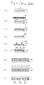
- a black matrix 4 is first formed on a glass substrate 1 and thereafter each of the color filter elements 3R, 3G and 3B are formed. While four methods of forming a color filter 3 have been employed up to present, a brief explanation will here be given of a pigment dispersion method and an electroplating method in the interest of convenience.
- a glass substrate 1 on which a black matrix 4 is formed as shown at (a) is coated over its entire surface with a coloring resist 13 for a said red color filter element 3R, as shown at (b), by the spin coating method or the roll coating method.
- the above mentioned coloring resist 13 is coated with a photo resist 14 by the spin coating method or the roll coating method.
- the layers 13 and 14 through a photo mask 15 are exposed to a light and developed to form red color filter elements 3R.
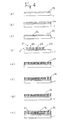
- a glass substrate 1 has an ITO (indium tin oxide) thin film 16 for electroplating formed thereon by the evaporation method, whereafter the said ITO thin film 16 is coated with a photo resist 14, as shown at (a). Then, as shown at (b), (c) and (d), the layers 14 and 16 are exposed through a photo mask 15 to a light and developed, and etched to form a stripe of the said ITO thin film 16.
- ITO indium tin oxide
- the glass plate 1 on which the said stripe of the ITO thin film 16 is formed is immersed in an electroplating or electro-depositing liquid in which particles of a pigment for a said red color filter element 3R are dispersed, and a positive voltage is applied between a pair of electrodes which are opposed to each other across the said ITO thin film 16 stripe so that those particles of the red pigment which have a particle size in the order of submicrons and are charged negative may electrolytically migrate towards the said ITO thin film 16 stripe charged positive and may then be electrolytically deposited on its surfaces.
- a said green color filter element 3G and a said blue color filter element 3B are electrolytically deposited by using respective electrolytic depositing or plating (i. e. electro-depositing or electroplating) liquids therefor.
- a color filter in a matrix 17 that comprises red, green and blue color filter elements 3R, 3G and 3B is formed on the said glass substrate 1 as shown at (f), referring continuingly to Fig. 3.
- a resinous black 18 having a photosensitivity is coated on the said color matrix 17 by the spin coating method or the roll coating method.
- the photosensitive resinous black 18 on the said colour matrix 17 will not be exposed to the said light in the presence of the intervening color filter elements 3R, 3G and 3B. And, it will be removed in the development process.
- a black matrix 4 will be formed in which the said resinous black 18 remains only between the adjacent ones of the said color filter elements 3R, 3G and 3B as shown at (i).
- a color filter 3 arrangement has an extremely large external size and requires a dimensional accuracy represented by a pixel pitch of 75 ⁇ m and a gap of 25 ⁇ m in the VGA (Video Graphic Array) specification, and a pixel of 70 ⁇ m and a gap of 20 ⁇ m in the SVGA (Super Video Graphic Array) specification and requires a positional accuracy per a panel of ⁇ 2 ⁇ m.
- VGA Video Graphic Array
- SVGA Super Video Graphic Array
- the present invention has been provided in view of the foregoing problems taken into account, and has for its object to provide a method of manufacturing a color display, whereby a color filter and a black matrix therein can be manufactured while not using at all a photo-lithographic step that is complicated and yet that requires a high degree of cleanness or using the latter step at the minimum, the black matrix can be manufactured having a high optical density and a low reflectivity as well as an enhanced aperture rate, and an arrangement of columnar cell gap controlling spacers therein which are precisely positionable can be obtained.
- a method of manufacturing a color display including a color filter and a black matrix characterized in that the said black matrix is prepared by the steps of: forming a film of zinc oxide on a transparent substrate; and applying a deposit of electroless copper plating onto the said film of zinc oxide while utilizing an catalytic action by palladium chloride, the said deposit constituting an element of the said black matrix.
- a color display may be provided with a black matrix that can be obtained which is of a high optical density and a low reflectivity.
- the invention also provides, in a second aspect thereof, a method of manufacturing a color display including a color filter and a black matrix, characterized in that it comprises the steps of: forming a film of zinc oxide on a transparent substrate; forming the said color filter on the said film of zinc oxide; and thereafter, applying a deposit of electroless copper plating on an area of the said film of zinc oxide on which the said color filter is not formed, the said deposit having a thickness which is substantially equal to a thickness of the said color filter and constituting an element of said black matrix.
- a color display may be provided simply with a black matrix that is commensurate in film thickness with the said color filter.
- a thin film of copper oxide is formed on a surface of the said deposit of electroless plating.
- a color display may be provided with a black matrix that can be obtained which is stable and of a low reflectivity as viewed from the side of the color filter.
- the said film of zinc oxide is doped with aluminum and is then used to serve as a transparent electroplating electrode as well.
- the said transparent substrate is a glass substrate, which may be made up of a soda glass.
- the said transparent substrate is made up of an organic film, which may be a polyester film.
- a driver integrated circuit is connected through a solder bump to the said electrolessly plated copper deposit.
- the invention also provides a third aspect thereof, a method of manufacturing a color display including a color filter and a black matrix, characterized in that said color filter is prepared by the steps of: forming a first film that is of a first color filter element of a first color which is selected from three primary colors: red R, blue B and green G over a surface of a glass substrate, and dividing, by means of eximer laser machining, the said first film into a plurality of color filter regions of the said first color; forming a second film that is of a second color filter element of a second color which has not been selected from the said three colors: R, B and G over such a surface of the said glass substrate as is exposed among the said first color filter regions of the said first color as a result of division of the said first film, and dividing, by means of eximer laser machining, the said second film into a plurality of color filter regions of the said second color; and forming a third film that is of a third color filter element of a third color which has not been
- the invention also provides, in a fourth aspect thereof, a method of manufacturing a color display including a color filter and a black matrix, characterized in that said color filter is prepared by the steps of: a) coating a surface of a glass substrate with a transparent electrode; b) forming a transparent film of a ferroelectric substance on the said transparent electrode; c) partially polarizing and charging the said transparent film of the ferroelectric substance in color filter forming regions thereof of a particular color; d) depositing on the said polarized and charged transparent film of the ferroelectric substance a color filter pigment of the said particular color that is reversely polarized and charged; and e) repetitively performing the steps c) and d) for the said color filter forming regions with respect to a red R, a blue B and a green G color as the said particular color.
- a color display may be provided with a color filter that can be prepared without using a photoresist step at all.
- the method set forth in the preceding paragraph may further comprises: providing a black matrix forming region in the said transparent film of the ferroelectric substance that is formed on the said transparent electrode; forming a polarization and charging preventive film on the said black matrix forming region; forming an electrolessly plated copper film on the said polarization and charging preventive film; and oxidizing at least partially the said electrolessly plated copper film.
- a color display may be provided with a black matrix that can be distinctly formed by preventing a color filter from being formed in a black matrix forming region.
- the invention also provides, in a still further aspect thereof, a method of manufacturing a color display including a color filter and a black matrix, characterized in that the said black matrix is prepared by the steps of: coating a surface of a glass substrate with a transparent electrode; forming a color filter on the said transparent electrode; forming on a surface portion of the said transparent electrode which has not been formed thereon with the said color filter and which is thus exposed a film of zinc oxide with the said transparent electrode serving as an electrically conducting terminal; forming an electrolessly plated copper film on the said film of zinc oxide; and oxidizing at least partially the said electrolessly plated copper film.
- a color display may be provided with a black matrix having a high aperture rate that can be formed simply and without using a photo step at all.
- the invention also provides, in yet a further aspect thereof, a method of manufacturing a color display including a color filter, a black matrix and a cell gap controlling spacer arrangement, characterized in that the said spacer assembly is prepared by the steps of: forming a glass substrate with a color filter having an uppermost layer constituted of a transparent electrode; forming a photo resist pattern on the said transparent electrode while using a mask for forming a spacer; forming a plurality of columnar spacers each composed of transparent zinc oxide by using a solution electrolysis process; and coating a surface of each of the said spacers with an insulating film of zinc oxide.
- a color display may be provided with an arrangement of spacers which are accurately positioned with a photo step that can be obtained without using a spacer spreading unit.
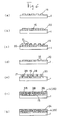
- Fig. 4 shows the form of a first embodiment of the method of preparing a black matrix in which a color filter is formed by a dyeing method, a pigment dispersion method, a printing method or the like.
- the glass substrate 1 will be formed with a film 20 of zinc oxide (ZnO) by sputtering or the like as shown at (a) in Fig. 4.
- the zinc oxide film 20 is a transparent oxide film which if it is a zinc oxide film having a thickness of 2000 to 3000 angstroms, has a transmissivity not less than 85 % in the visible light range of the said substrate glass.
- the said zinc oxide film 20 will be formed by a photo process with a pixel section 21 and a driver circuit section 22 patterned as shown at (c).
- the above mentioned pixel section 21 that has been formed by the photo process will be formed, by the dyeing method, the pigment dispersion method, the printing method or the like, on the above mentioned zinc oxide film 20 with a color matrix 17 that comprises red, green and blue color filter elements.
- the color matrix 17 will have a film thickness which is considered to be of 1 to 2 ⁇ m.
- the said glass substrate 1 formed with the said color matrix 17 will be immersed in a solution of palladium chloride (PdCl 2 ) having a catalytic action for a period of 1 to 2 minutes to adsorb Pd ions on its exposed outer surfaces.
- the resulting glass substrate 1 will be immersed in an electroless copper plating solution to allow a copper component 23 to be electrolessly deposited thereon with a thickness corresponding to the film thickness of the said color matrix 17 as shown at (e) in Fig. 4.
- the above mentioned palladium chloride solution may, as an example, have a composition of 0.2 g of PdCl 2 , 0.5 ml of HCl and 500 ml of H 2 O.
- the said copper component 23 will be selectively deposited only on a portion at which the said zinc oxide film 20 is exposed and may not be deposited on a portion on which the said color matrix 17 has been formed. This indicates that the said color matrix 17 plays a role as a mask. As a consequence, a black matrix 4 can be formed automatically, without requiring any photo process at all.
- the said copper component 23 that has been deposited at the above mentioned pixel section 21 will, as seen from the side of the said glass substrate 1 located backwards, be viewed in a black color because of the appearance of a surface plasmon polariton (SPP) which is to be described later, but will, as seen from the side at which the said color matrix 17 has been formed, be viewed in a color of copper itself having a metallic brightness. Thus, in this state, it has a high reflectivity to a back light and is poor in its utility. Therefore, as shown at (f) in Fig. 4, the said driver circuit section 22 should be masked with photo resists 14 and the said glass substrate 1 as a whole will be immersed in a solution that is capable of oxidizing the copper component, e.
- SPP surface plasmon polariton
- the said photo resist 14 that has masked the said driver circuit section 22 will be removed, whereupon the said pixel section 21 will be formed with a said ITO thin film 16 for display and will thus be electrically connected to the said driver circuit section 22 having the said copper component 23 deposited on the said zinc oxide film 20.
- a driver IC 25 will be applied to the said driver circuit section 22 at an exposed copper component 23.
- a black matrix 4 can be prepared simply and inexpensively without requiring a photo process.
- plasma polariton that involves the vibration of an electromagnetic field (and that results from a combination of the vibration of particles and the vibration of an electromagnetic field).
- plasma polariton since a metal or a semiconductor has on its surface a vibrational mode called "plasma polariton", it may be able to absorb lights whose phase velocities become identical to one another. In general, lights having different phase velocities are not absorbed by a metal having a smooth surface.
- the black matrix 4 that is prepared according to the present form of embodiment of the invention will enable the surface plasmon polariton to be excited at the said surface irregularity with lights in the visible range and, as a result, will exhibit a tremendous visible light absorptivity, as represented at the interface between the copper deposition component 23 and the zinc oxide film 20 by its optical density (OD) being 5, thus putting an enhanced aperture rate into reality.
- OD optical density
- an active matrix liquid crystal display makes use of a glass substrate 1 that is constituted of a non-alkaline glass substrate or a silica glass substrate and that an STN (Super Twisted Nematic) liquid crystal display makes use of a glass substrate which is coated with SiO 2 .
- the zinc oxide film 20 acts to prevent the alkaline from being dissolved and hence can omit the step of coating the soda glass with SiO 2 , thus permitting a further cost-down to be achieved.
- a driver IC is mounted on both one glass substrate 1 at the side of a color filter and the other glass substrate.
- ACF Adisotropic Conductive Film
- Figs. 5 to 7 of the drawings attached hereto show a form of embodiment in which the present invention is applied to the method of preparing a color filter assembly by using an electroplating or electro-depositing technique.
- Fig. 5 is a top plan view that illustrates a color filter prepared according to the electroplating or electro-depositing technique.
- color filter elements 3R, 3G and 3B are arranged in a cellular form to stand in lines, color by color, with each thereof being surrounded by elements of a black matrix 4.
- This form of embodiment of the invention is designed to provide a black matrix 4 which is clearer in picture quality than the conventional black matrix 4.
- Fig. 6 is a set of cross sectional views taken along the line III -III in Fig. 5 whereas Fig. 7 is a set of cross sectional views taken along IV -IV in Fig. 5.
- a glass substrate 1 will be formed, as shown at (a), with a discontinuous ITO thin film 16 in the form of a stripe for the purpose of electroplating.
- the said glass substrate 1 and the said ITO thin film 16 will be formed thereon, by a sputtering or the like technique, with a film of zinc oxide 20 until its thickness is grown to 2000 to 3000 angstroms.
- areas other than pixel portions 21 of a color filter 3 will be masked with a discontinuous photo resist 14 and the said oxide film 20 in areas at the said pixel portions 21 will be removed by etching.
- the said ITO thin film 16 at those pixel portions 21 and the said film of zinc oxide 20 in the areas other than those portions 21 are made substantially equal to each other in thickness.
- the said discontinuous ITO thin film 16 will be formed thereon, by electroplating, with a color matrix 17 which comprises red color filter elements 3R, green color filter elements 3G and blue color filter elements 3B. And, after the said color matrix 17 has been formed, the glass plate 1 will be immersed in a palladium chloride (PdCl 2 ) solution to allow Pd ions to be adsorbed onto the said film of zinc oxide 20 and will then be subjected to an electroless copper plating process to form a black matrix 4 which consists of copper deposits 23 electrolessly plated, as shown at (f) in Fig. 6.
- PdCl 2 palladium chloride
- any copper component will never be electrolessly deposited on the said color matrix 17.
- the said copper deposits 23 on the said film of zinc oxide 20 will have a thickness that is substantially equal to the thickness of the said color matrix 17.
- the above mentioned black matrix 4 has a copper surface having a metallic brightness, it is desirable that in order to reduce the reflectivity for a back light the same should be immersed in, for example, water of hydrogen peroxide or nitric acid to convert the surfaces of the said copper deposits 23 into a discontinuous film of copper oxide 24, as shown at (g) in Fig. 6.
- Fig. 7 is a set of cross sectional views taken alone the line IV -IV in Fig. 5 previously described, the section shown represents a cross arrangement of a portion in which a said discontinuous ITO thin film 16 for the purpose of electroplating is disposed in the form of a stripe and a series of spacings where the said ITO film 16 are removed.
- a black matrix 4 there in a transverse direction in the Figure as shown at (a) a said film of zinc oxide 20 as formed on a said glass plate 1 and the said discontinuous ITO thin film 16 as in Fig. 6(b) previously described will be masked with a said photo resist 14 as shown at (b) in Fig.
- a said black matrix 4 can be formed simply and expensively, without requiring the photo step.
- a said film of zinc oxide 20 that is used as rendered electrically conductive by being doped with aluminum is capable of playing two roles as the said ITO thin film for the purpose of electroplating and as the base in the formation of the said black matrix 4.
- Fig. 8 shows a third form of embodiment of the present invention.
- the stripe of a said ITO thin film for electroplating is used in electroplating a said color filter, it employs a patternless method using the overall surface of a said ITO thin film, without photoetching the same.
- an explanation will be given of an example using a film of zinc oxide that is doped with aluminum, as prepared by using a target of zinc oxide which contains 2 % by weight Al 2 O 3 instead of a said ITO thin film.
- a film of zinc oxide that is doped with aluminum can provide materials ranging from an electrical insulator to an electrical conductor having an electrical resistivity not greater than 3x10 -4 ⁇ ⁇ cm.
- a said glass substrate 1 will be formed with an aluminum doped zinc oxide film 26 (that is a film of zinc oxide doped with aluminum by sputtering) until its thickness is grown to 2000 to 3000 angstroms. Over the entire surface of the said aluminum doped zinc oxide film 26, there will be electrolytically plated a red color filter element 3R layer over which a said photo resist 14 is coated.
- an aluminum doped zinc oxide film 26 that is a film of zinc oxide doped with aluminum by sputtering
- the said layer will be pattern exposed to a light via the said photo resist 14 to provide a said red color filter element 3R, and the color filter element 3R material that is electroplated on the said aluminum doped zinc oxide film 26 at those portions which are other than such color filter 3R elements will be removed by development, as shown at (c). It should be noted at this point that those photo resists 14 on the color filter elements 3R will be left intact. Then, each set of green color filter elements 3G and blue color filter elements 3B will be formed similarly with a series of the procedures (a) to (c) that is repetitively performed.
- the said glass substrate 1 which has been formed with the color filter 3 will be immersed in a palladium chloride (PdCl 2 ) solution to allow Pd ions to be adsorbed onto the said aluminum doped zinc oxide film 26. Thereafter, the said glass substrate 1 will be immersed in an electroless copper plating solution to apply copper deposits 23 onto those portions at which the said color filter 3 was not electroplated and the said aluminum doped zinc oxide film 26 is exposed, thereby forming a black matrix 4 as shown at (e) in Fig. 8. The thickness of the said black matrix 4 will then be made substantially equal to the thickness of the said color filter elements 3R, 3G and 3B.
- PdCl 2 palladium chloride
- the said glass substrate 1 will be immersed in water of hydrogen peroxide or a solution of nitric acid to lightly oxidize the surfaces of the said copper deposits 23, thereby forming a black colored thin film of copper oxide 24, as shown at (f) in Fig. 8.
- the photo resist 14 on each of the color filter elements 3 will be removed, thus completing a color matrix 17 defined by the said black matrix 4.
- the present invention will allow a transparent organic film such as a polyester film, other than a glass, to be used as the said substrate.
- a transparent organic film such as a polyester film, other than a glass
- a polyester film has been tested in applying the present invention thereto and it has been confirmed to achieve the effects which are similar to those attained with a glass substrate. It may be noted, however, that an organic film is relatively poor in heat resistivity as compared with a glass and, for this reason, a selection thereof should be made to use a material which does not cause an adverse thermal influence on the substrate that is formed with a film of zinc oxide by a sputtering or the like technique.
- the present invention is not limited to the electroless copper plating but may utilize electroless plating of any other metal.
- the present invention enables a black matrix to be manufactured simply and inexpensively, yet having a high optical density and a low reflectivity.
- a film of zinc oxide on a transparent substrate, forming a color filter on the said film of zinc oxide and thereafter applying a deposit of electroless plating onto those portions of the said film of zinc oxide which are not formed with the said color filter while utilizing a catalytic action by means of palladium chloride so that the said deposit of electroless copper plating may have a thickness which is substantially equal to the thickness of the said color filter, it has been noted that a black matrix with the thickness commensurate with the thickness of the color filter can be simply prepared.
- the glass substrate that may be composed of a soda glass.
- a black matrix can be formed that corresponds to a color film liquid crystal display device.
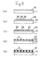
- Fig. 9 shows another form of embodiment of the method according to the present invention, in which a color filter is formed by a dyeing method, a pigment dispersion method, a film transfer printing method or the like and thereafter a black matrix is formed.
- a glass substrate 1 will be formed, by a sputtering or the like film forming technique, with a transparent ITO (indium tin oxide) electrode film 16 until its thickness is grown to 500 to 1000 angstroms.
- a color filter 3 of red, green and blue color filter elements 3R, 3G and 3B will be formed on the said ITO transparent electrode film 16 by using any one of color filter preparation methods mentioned earlier.
- the said color filter will have a film thickness in a range from 1 to 2 angstroms.
- a film of zinc oxide (ZnO) 20 will be formed, using a solution electrolysis method, on those surface portions of the ITO transparent electrode 16 which have not been formed with the R, G and B color filter elements 3R, 3G and 3B and which represent a black matrix forming region.
- the zinc oxide component that constitutes the said film 20 can be cathodically deposited in an aqueous solution of zinc nitrate having a pH of 5.2 with a zinc anode to which a voltage of -0.7 to -1.0 volt is applied.
- the above mentioned transparent electrode 16 functions to serves as a power supply electrode also for the purpose of cathodically depositing the said zinc oxide component.
- the time period that is required to cathodically deposit the said film of zinc oxide 20 of a thickness of 0.15 to 0.3 micron has been found to be 2 to 3 minutes.
- the said glass substrate 1 that has been formed with the said color filter 3 will be immersed in solution of palladium chloride (PdCl 2 ) having a catalytic action for a period of 1 to 2 minutes to allow Pd ions to be adsorbed onto the said transparent electrode 16, whereupon it will be immersed in an electroless copper plating solution to electrolessly form a copper deposit 23 on the said film of zinc oxide 20 until the said copper deposit has a thickness that is commensurate with the thickness of the said color filter 3.
- the above mentioned solution of palladium chloride may have, for example, a composition having 0.2 g of Pd Cl 2 , 0.5 ml of HCl and 500 ml of H 2 O.
- the said copper deposit 23 will be selectively applied onto those surface portions of the film of zinc oxide 20 where it is exposed, and may not be formed on such surface portions thereof as are formed with the said color filter 3. This is because the said color filter 3 plays a role as a mask. It follows, therefore, that a black matrix 4 can be formed in a self-alignment without using a photo step at all.
- the said copper deposit 23 of the black matrix 4 will. as seen from the side of the said glass substrate 1 located backwards, be viewed in a black color because of the appearance of a surface plasmon polariton (SPP) which is to be described later, but will, as seen from the side at which the said color filter 3 has been formed, be viewed in a color of copper itself having a metallic brightness.
- SPP surface plasmon polariton
- the said glass substrate 1 will as a whole be immersed in a solution that is capable of oxidizing a copper component, e. g., water of hydrogen peroxide or a solution of nitric acid, in order to convert the surface of the said copper deposit 23 into a thin film 24 of copper oxide (CuO) having a low reflectivity.
- a solution that is capable of oxidizing a copper component e. g., water of hydrogen peroxide or a solution of nitric acid
- CuO copper oxide
- a heat treatment in an oxygen atmosphere may be employed as well to convert the surface of the copper deposit 23 into a said thin film of copper oxide 24.
- plasma polariton that involves the vibration of an electromagnetic field (and that results from a combination of the vibration of particles and the vibration of an electromagnetic field).
- plasma polariton since a metal or a semiconductor has on its surface a vibrational mode called "plasma polariton", it may be able to absorb lights whose phase velocities become identical to one another.
- the black matrix 4 that is prepared according to the present form of embodiment of the invention will enable the surface plasmon polariton to be excited at the said surface irregularity with lights in the visible range and, as a result, will exhibit a tremendous visible light absorptivity, as represented at the interface between the copper deposition component 23 and the zinc oxide film 20 by its optical density (OD) being 5, thus putting an enhanced aperture rate that is much higher than in the prior art, into reality.
- OD optical density
- Fig. 10 illustrates a certain form of embodiment of the present invention in which a color filter is prepared by using laser ablation and without using at all a photo resist step that is complicated.
- a said glass plate 1 has preliminarily been formed, by a sputtering or the like technique, with a said ITO transparent electrode 16 so that it may have a thickness of around 1000 angstroms.
- any one of the pigment dispersion method, the dyeing method, the film transfer method is applicable, but an explanation will here be given with exemplary reference to the electroplating method that that has been known to be the most simple among the others.
- a film for a red (R) color filter element 3R will be electroplated over the entire surface of the said glass substrate 1 with the said ITO transparent electrode 16 serving as an electroplating electrode. Then, the said film for R will be laser ablated by an eximer laser, via a color filter R forming pattern to form R color filter elements 3R as shown at (c) in Fig. 10.
- An eximer laser is an ultraviolet laser and is able to form a pattern by machining a workpiece through laser ablation. Its machining depth is also controllable with a number of laser pulses.
- the eximer laser machining is a technology that has been widely employed for machining fine small holes (e. g., via holes and through holes) in a polyimide workpiece that may constitute a flexible printed circuit board, a thin film laminated substrate or the like in recent years.
- a laser light that is emitted from an eximer laser oscillator 30 is passed through a laser shaping system 31, and its utility efficiency is enhanced through a multi-reflection optical system 40 that comprises a high reflectivity mask 33 and a high reflectivity mirror 32. Then, with a pattern gained through a high reflectivity mask 37 and passing through a focusing optical system 34, the laser light is controlled to illuminate a workpiece 36 and while it is being viewed with a monitor 35 is used to ablate the workpiece 36.
- the said mask 37 and the said workpiece 36 are scanned by a scanning system 38 under the control of a CNC controller 39 to carry out a desired ablation machining operation over an entire surface of the workpiece 36.
- Fig. 13 illustrates details of an ablation machining operation while a said mask 37 and a said workpiece 36 are being scanned.
- the said mask 37 and the said workpiece 36 will be placed each as movable so that a laser light passed through a pattern a of the mask 37 may be focused through a said focusing optical system 34 to illuminate the workpiece 36, imparting thereto an ablation machined pattern a '. Then, as shown at (b), (c) and (d) in succession, the said mask 37 and the said workpiece 36 will each be intermittently displaced so that when they are stopped, the laser light passed through b , c d and e of the mask 37 may be focused to illuminate the workpiece 35, thereby imparting thereto ablation machined patterns a ', b ', c ' and d '.
- a film for a green G color filter element 3G will be electroplated over the entire pixel section except the red R color filter elements 3G by the electroplating method.
- the eximer laser will be applied via a said imaging mask 37 for forming a said color filter element 3G to machine through laser ablation blue B color filter 3B forming regions.
- a film for a blue B color filter element 3B will be electroplated onto those regions of the said transparent electrode 16 which are exposed, by the electroplating method. It will be apparent that the said glass substrate 1 in this stage has thereon the three color filter elements 3R, 3G and 3B arranged with no interstice whatsoever therebetween, as shown at (f). Then, as shown at (g), using the black matrix forming mask 35 the black matrix forming regions will be machined through laser ablation. Then, as shown at (h), the color filter 3 will be removed by laser ablation so that a said film of zinc oxide 20 may be formed by the solution electrolysis method on those surface portions of the transparent electrode 16 which are exposed.
- a said copper deposit 23 will be applied by the electroless plating method upon the said film of zinc oxide 20. Thereafter, as shown t (j), a said film of copper oxide 24 will be formed on a surface of the said copper deposit 23 by an oxidation treatment.
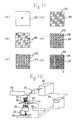
- Fig. 11 there is shown a feature of the laser ablation method in which the color filter elements 3R, 3G and 3B if to be arranged in a triangular or a mosaic pattern can be simply formed by only changing the imaging mask, this being shown in its steps with exemplary reference to a said mosaic pattern.
- a film for a red R color filter element will be electroplated on the said transparent electrode 16. Then, as shown at (b), the said film will be removed except for those regions in which the color red R filter elements 3R are to be formed as are originally intended. Further, as shown at (c), a film for a green G color filter element 3G will be electroplated over the entire area of the transparent electrode 16 from which the film for a said red R color element has been removed. Then, as shown (d), those portions of the film for a said green G color element which are to be formed with blue B color filter elements 3B will be removed by the eximer laser. Then, as shown at (e), a film for a said blue color filter element 3B will be electroplated. Further, as shown at (f), those portion of this film which represent black matrix forming regions will be removed by the eximer laser.
- Figs. 14 to 16 illustrate certain forms of embodiment of the present invention which are limited to the use of an electroplating method.
- an electroplating method it should be noted that it has hither been difficult to form any relevant thing other than a black matrix. Now, an explanation will be given of a method of manufacturing for providing a desired formation by taking the advantage in the electroplating method for a black matrix.
- Fig. 14 is a top plan view that illustrates a color filter as prepared in the electroplating method
- Fig. 15 is a series of step views in cross section taken along the line A-A in Fig. 14
- Fig. 16 is a series of step views in cross section taken along the line B-B in Fig. 14.
- a said glass plate 1 will be formed, by a sputtering or the like technique, with a said ITO transparent electrode 16 until its thickness is grown to around 0.1 micron, and a transparent electrode strip 16' for the purpose of electroplating a color filter film will be formed by means of a series of photo resists 14.
- the said glass substrate 1 will be immersed in an aqueous solution of a temperature of 50 °C and containing zinc nitrate and dimethylaminoborane (DMAB) for a period of about 20 minutes to form an insulating film of zinc oxide 20 with a film thickness of 0.2 micron. Then, the said photo resists 14 will be removed to form a said transparent electrode 16 and a said film of zinc oxide 20 in a state in which they are cross arranged, as shown at (d).
- DMAB dimethylaminoborane
- the said color filter elements 3R, the said color filter elements 3G and the said color filter elements 3B will be electroplated in succession.
- an electroless plating process will be carried out to form a said copper deposit 23 ay each of those portion in which a said film of zinc oxide 20 has been formed, as shown at (f).
- a surface of the said copper deposit 23 will be oxidized to form a said film of copper oxide 24, thus completing a black matrix 4.
- Fig. 16 is a set of step views in cross section taken along the line B-B in Fig. 14, in which the steps (a) to (d) are identical to (a) to (d) in Fig. 15.
- the said photo resist 14 will be removed as shown at (f) in Fig. 16, and those exposed portions of the transparent electrode 16 which correspond to the said transverse stripe will be electroplated with a film of zinc oxide 20' by a solution electrolysis method. Then, the said color filter substrate 1 will be immersed in an electroless copper plating solution to allow a film of copper 23 to be deposited on the said film of zinc oxide 20' as shown at (g). Finally, as shown at (h), a surface of the said copper film 23 will be oxidized to form a film of copper oxide 24, thus completing a black matrix 4.
- the glass substrate After washing, the glass substrate will be immersed in a sensitizer liquid containing 1 g/dm -3 of SnCl 2 ⁇ 2H 2 O and 1.0 ml/dm -3 of 37 % HCl for several minutes and then will be immersed in an active ⁇ liquid containing 0.1 g/dm -3 of PdCl 2 and 0.1 ml/dm -3 of 37 % HCl.
- the said glass substrate 1 After having been subjected to the above mentioned preliminary treatment, the said glass substrate 1 will be immersed in the aqueous solution that is heated to about 50 °C and that contains 0.05 mol/l of zinc nitrate and 0.001 to 0.15 mol/l of dimethylboran (DMAB). Then, after a lapse of time of about 20 minutes, a film of zinc oxide 20 of a thickness of 0.2 micron will be formed on the said glass substrate 1.
- DMAB dimethylboran
- a film 20 that is formed according to the above mentioned method is characterized in that it is high in its insulation properties. This fact constitutes a favorable feature since a high resistivity is required for a zinc oxide material that is used as the base of a black matrix where a color filter is formed by an electroplating method, although a high resistance zinc oxide film 20 that is used as the said transparent electrode is a problem.
- a said glass matrix 1 will be formed over its entire surface with a said ITO transparent electrode 16 by a sputtering or the like technique until its thickness is grown to 500 to 1000 angstroms.
- a transparent film 25 of a ferroelectric substance such as PZT
- the said film of the ferroelectric substance 25 will be coated over its entire a zinc oxide material having a photosensitivity by a spin coating or roll coating method and then will be preliminarily baked.
- a DC filed will be applied between the said transparent electrode 16 poled negative on the said glass substrate 1 and the positively poled regions where red R color filter elements 3R are to be formed, to produce a residual plus polarization on the surface of the said film of the ferroelectric substance 25, as shown at (d).
- the polarization to this end may be carried out either by polarizing the entire surface of the color filter at a one time with a two-dimensional stylus or successively polarizing the same with a one-dimensional stylus.
- the said glass substrate 1 on which the said color filter elements 3R have been polarized will be immersed in a micell electrolyte in which particles of an organic pigment for a red color filter element 3R are dispersed.
- the said particles of the organic pigment of the color filter elements 3R will be charged negative by the presence of a micellized substance so that, as shown at (e), the said color filter elements 3R may be deposited onto the said film of the ferroelectric substance 25 whose surface is polarized positive.
- the color filter elements 3G and the color filter elements 3B will be deposited onto the said glass substrate 1.
- the said glass substrate 1 on which the said color filter elements 3R, 3G and 3B have been formed will be immersed in an electroless copper plating liquid to apply a copper deposit 23 on each of the portions which are to constitute a black matrix, as shown at (g).
- the surface of the said copper deposit or film 23 will be oxidized to form a film of copper oxide 244 thereon.
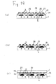
- Fig. 18 illustrates a certain form of embodiment of the method of preparing a cell gap controlling spacer arrangement according to the present invention.
- a black matrix 4 and a color filter 3 have been formed on a said glass substrate 1, by using any of the methods mentioned earlier
- the color filter elements 3 are covered with a protective film 26.
- an ITO thin film 16 constituting the transparent electrode will be formed on the above mentioned protective film 26 by a sputtering or evaporation method, and a photo resist pattern 27 for the purpose of forming spacers will be formed on the said ITO thin film 16 by using a spacer forming mask.
- a plurality of square columnar spacers 28, 28, ... for controlling cell gaps each of which consists of a transparent zinc oxide component, will be formed as spaced apart from one another with a predetermined spacing, by a solution electrolysis method, lying at portions not covered by the said photo resist pattern 27 and being connected to the said ITO thin film 16. It can be seen that the top of each of the said spacers 28 is projected upwards of the said photo resist pattern 27. Then, by using an immersion method, the surface of each of the said spacers 28 will be coated with a highly insulating film of zinc oxide 29.
- each of the said spacers 28 may be cylindrical.
- a liquid crystal display device can be manufactured as shown at (c) in Fig. 18 by attaching a unit with the said substrate 1 as assembled as above to another substrate 1 with an ITO thin film 16 and so forth with the use of the said cell gap controlling spacers 28 and sealing a liquid crystal in the construction so attached.
- an arrangement of spacers which are accurately positioned in a photo step without a spacer spreading unit can be prepared to enable a liquid crystal display device to be created with a predetermined thickness.
Abstract
There is provided a method of manufacturing a color display including a color filter and a black matrix, characterized in that it comprises the steps of: forming a film of zinc oxide on a transparent substrate; forming the the color filter on the said film of zinc oxide; and thereafter, applying a deposit of electroless copper plating on an area of the said film of zinc oxide on which the said color filter is not formed, the said deposit having a thickness which is substantially equal to a thickness of the said color filter and constituting an element of said black matrix. Thus, a color display may be provided with a black matrix that is of high optical density and a low reflectivity. The black matrix can also be commensurate with film thickness with the color matrix. No photo lithographic process is required in preparing the color filter and black matrix. Various modified forms of embodiments of the method of manufacturing a color display are also disclosed.
Description
- The present invention relates to a black matrix as well as a color filter for use in a color (flat) display such as a liquid crystal display, a thin film EL display or a field emitter display device to obtain a clear color display. More particularly, the invention relates to a method of manufacturing a color (flat) display, whereby the black matrix and the color filter may be prepared with an enhanced aperture rate and they as well as a cell gap controlling spacer arrangement can be prepared without a photo lithographic process that has hitherto had to be used despite of its complicated handling procedures.
- An explanation will first be given of a typical color liquid crystal display device with reference to Fig. 1 of the drawings attached hereto.
- In Fig. 1, there is shown a pair of
glass substrates glass plate 1A has, outside thereof, apolarization plate 2A bonded thereto and has, inside thereof, a number ofcolor filter elements color filter elements black stripe 4 that is designed to effect a glare protection and thus to obtain a clear color display. Of them, the black stripe is used exclusively for an electroplated color filter. Hence,numeral 4 here is used hereinafter in connection with the present invention to refer to a black matrix or black matrix element. Also, inside of thecolor filter 3 and theblack matrix 4 mentioned above, there is disposed via a protective filter 5 atransparent electrode 6A. - On the other hand, outside of the other 1B of the above mentioned glass substrates, there is disposed via a
polarization plate 2B a light illuminating plate 7 that functions to provide a back light. In the vicinity of an end surface of the said light illuminating plate 7, there is disposed afluorescent lamp 8 that is adapted to cause the said light illuminating plate 7 to emit a light from over a surface thereof. Also, inside of the above mentionedglass substrate 1B, there are so arranged a plurality ofgates 10 as are covered with aninsulating layer 9. Further, inside of the saidinsulating layer 9, there are arranged hydrogenated amorphousthin film transistors 11, which are switching elements in opposition to the above mentionedgates 10, in a manner such that they may be surrounded with their respectiveprotective members 12. And, inside of the above mentionedinsulating layer 9, there are arrangedtransparent electrodes 6B, each associated with a said hydrogenated amorphousthin film transistor 11 for supplying the same with an electric current, respectively. It should also be noted that a liquid crystal LC is sealed in a tightly closed space between the above mentionedtransparent electrodes - An explanation will now be given with respect the functions of the above mentioned
black matrix 4 in a liquid crystal color display device as mentioned above. If the saidblack matrix 4 is held in the state in which the greencolor filter element 3G is turned ON and the redcolor filter element 3R and the bluecolor filter element 3B which are adjacent thereto are each turned OFF, it will function in a manner such that the back light which is surface emitted from the said light illuminating plate 7 may be transmitted only through the saidgreen color filter 3G that is in the ON state and may not reach the said red andblue color filters - And, the said
black light matrix 4 is required to be composed of a material that is not only capable of shielding the back light but is of a low reflectivity to the back light. This is because if the greencolor filter element 3G is in the ON state and the red and bluecolor filter elements black matrix 4 has a high reflectivity to the back light a said back light that is reflected at theblack matrix 4 will be incident to those hydrogenated amorphousthin film transistors 11 which are each in the OFF state, corresponding to the red and bluecolor filter elements transistors 11 each into the ON state. - By the way, from the standpoint of the requirement for a lower reflectivity, a resinous black may be used as a composition for a
black matrix 4 to provide a reflectivity that is as low as 0.5 %, and is thus found to be much superior to a metallic chromium composition having a reflectivity of 50 % and to a low reflection chromium composition having a reflectivity of 30 % or less. Ablack matrix 4 that is composed of the resinous black has the problem, however, that its optical density (OD) which is an index that is indicative of a light shielding performance for the back light is 2.3 which is lower than 4 or more with the metallic chromium composition or the low reflection chromium. For this reason, a low reflection composition in which a chromium oxide component is mounted on a metallic chromium component is now becoming a leading composition for ablack matrix 4. - An explanation will next be given with respect to a method of preparing a
black matrix 4. In a method other than an electroplating method, ablack matrix 4 is first formed on aglass substrate 1 and thereafter each of thecolor filter elements color filter 3 have been employed up to present, a brief explanation will here be given of a pigment dispersion method and an electroplating method in the interest of convenience. - First, an explanation will be given of the pigment dispersion method.
- Referring to Fig. 2, a
glass substrate 1 on which ablack matrix 4 is formed as shown at (a), is coated over its entire surface with acoloring resist 13 for a said redcolor filter element 3R, as shown at (b), by the spin coating method or the roll coating method. Then, as shown at (c), the above mentionedcoloring resist 13 is coated with aphoto resist 14 by the spin coating method or the roll coating method. Further, as shown at (d) and (e), thelayers photo mask 15 are exposed to a light and developed to form redcolor filter elements 3R. - Thereafter, by repeating a procedure as mentioned above with respect to a said green
color filter element 3G and a said bluecolor filter element 3B, eventually the threecolor filter elements - Next, an explanation will be given of the electroplating method.
- Referring to Fig. 3, a
glass substrate 1 has an ITO (indium tin oxide)thin film 16 for electroplating formed thereon by the evaporation method, whereafter the said ITOthin film 16 is coated with aphoto resist 14, as shown at (a). Then, as shown at (b), (c) and (d), thelayers photo mask 15 to a light and developed, and etched to form a stripe of the said ITOthin film 16. Thereafter, as shown at (e), theglass plate 1 on which the said stripe of the ITOthin film 16 is formed is immersed in an electroplating or electro-depositing liquid in which particles of a pigment for a said redcolor filter element 3R are dispersed, and a positive voltage is applied between a pair of electrodes which are opposed to each other across the said ITOthin film 16 stripe so that those particles of the red pigment which have a particle size in the order of submicrons and are charged negative may electrolytically migrate towards the said ITOthin film 16 stripe charged positive and may then be electrolytically deposited on its surfaces. Subsequently, a said greencolor filter element 3G and a said bluecolor filter element 3B are electrolytically deposited by using respective electrolytic depositing or plating (i. e. electro-depositing or electroplating) liquids therefor. - In this manner, a color filter in a
matrix 17 that comprises red, green and bluecolor filter elements said glass substrate 1 as shown at (f), referring continuingly to Fig. 3. Then, as shown at (g), a resinous black 18 having a photosensitivity is coated on the saidcolor matrix 17 by the spin coating method or the roll coating method. Thereafter, if thesaid glass substrate 1 is exposed to a back light in the form of ultraviolet (UV) rays as shown at (h), the photosensitive resinous black 18 on thesaid colour matrix 17 will not be exposed to the said light in the presence of the interveningcolor filter elements black matrix 4 will be formed in which the said resinous black 18 remains only between the adjacent ones of the saidcolor filter elements - By the way, unlike a semiconductor IC a
color filter 3 arrangement has an extremely large external size and requires a dimensional accuracy represented by a pixel pitch of 75 µm and a gap of 25 µm in the VGA (Video Graphic Array) specification, and a pixel of 70 µm and a gap of 20 µm in the SVGA (Super Video Graphic Array) specification and requires a positional accuracy per a panel of ± 2 µm. Hence, it has adopted its manufacturing process which relies much on a photo step, if the process were not the printing method. - And, it has been recognized that the printing method will be unable to meet with the requirement in the future that the mother glass should be much more large sized and the pixel should be made increasingly finer.
- In forming a color filter arrangement according to a conventional method, there has also been a fear that due to the presence of a difference in level between a
color filter 3 and ablack matrix 4 arising from a difference between the film thicknesses, a problem of step coverage may be created at a location where there is such a difference in level. This has hitherto required the said difference in level to be filled up by coating a transparent resin over the entire surface and, if needed, the coated surface to be further processed by polishing, thus rendering the process much complicated. - The present invention has been provided in view of the foregoing problems taken into account, and has for its object to provide a method of manufacturing a color display, whereby a color filter and a black matrix therein can be manufactured while not using at all a photo-lithographic step that is complicated and yet that requires a high degree of cleanness or using the latter step at the minimum, the black matrix can be manufactured having a high optical density and a low reflectivity as well as an enhanced aperture rate, and an arrangement of columnar cell gap controlling spacers therein which are precisely positionable can be obtained.
- In order to achieve the object mentioned above, there is provided in accordance with the present invention, in a first aspect thereof, a method of manufacturing a color display including a color filter and a black matrix, characterized in that the said black matrix is prepared by the steps of: forming a film of zinc oxide on a transparent substrate; and applying a deposit of electroless copper plating onto the said film of zinc oxide while utilizing an catalytic action by palladium chloride, the said deposit constituting an element of the said black matrix.
- By adopting the construction mentioned above, it should be noted that a color display may be provided with a black matrix that can be obtained which is of a high optical density and a low reflectivity.
- The invention also provides, in a second aspect thereof, a method of manufacturing a color display including a color filter and a black matrix, characterized in that it comprises the steps of: forming a film of zinc oxide on a transparent substrate; forming the said color filter on the said film of zinc oxide; and thereafter, applying a deposit of electroless copper plating on an area of the said film of zinc oxide on which the said color filter is not formed, the said deposit having a thickness which is substantially equal to a thickness of the said color filter and constituting an element of said black matrix.
- By adopting the configuration set forth above, it should be noted that a color display may be provided simply with a black matrix that is commensurate in film thickness with the said color filter.
- According to a certain feature of the present invention, that is concomitant with the above mentioned aspects thereof, a thin film of copper oxide is formed on a surface of the said deposit of electroless plating.
- By adopting the construction mentioned above, it should be noted that a color display may be provided with a black matrix that can be obtained which is stable and of a low reflectivity as viewed from the side of the color filter.
- According to another feature of the present invention, that is concomitant with the above mentioned aspects thereof, the said film of zinc oxide is doped with aluminum and is then used to serve as a transparent electroplating electrode as well.
- By adopting the construction mentioned above, it should be noted that there will be no need to provide the said ITO transparent electrode separately.
- According to another feature of the present invention, that is concomitant with the above mentioned aspects thereof, the said transparent substrate is a glass substrate, which may be made up of a soda glass.
- It should be noted that these arrangements are enabled because the said zinc oxide is effective to prevent an alkaline dissolution.
- According to another feature of the present invention, that is concomitant with the above mentioned aspects thereof, the said transparent substrate is made up of an organic film, which may be a polyester film.
- By adopting such a construction as set forth above, it should be noted that an further inexpensive black matrix and hence such a color display can be provided.
- According to another feature of the present invention, that is concomitant with the above mentioned aspects thereof, a driver integrated circuit is connected through a solder bump to the said electrolessly plated copper deposit.
- By adopting such a construction as set forth above, it should be noted that in a color display such as an STN (Super Twisted Nematic) liquid crystal display, there will be no need to provide an expensive bump such as a metallic bump, and a direct bonding to the said IC glass substrate will be made possible.
- The invention also provides a third aspect thereof, a method of manufacturing a color display including a color filter and a black matrix, characterized in that said color filter is prepared by the steps of: forming a first film that is of a first color filter element of a first color which is selected from three primary colors: red R, blue B and green G over a surface of a glass substrate, and dividing, by means of eximer laser machining, the said first film into a plurality of color filter regions of the said first color; forming a second film that is of a second color filter element of a second color which has not been selected from the said three colors: R, B and G over such a surface of the said glass substrate as is exposed among the said first color filter regions of the said first color as a result of division of the said first film, and dividing, by means of eximer laser machining, the said second film into a plurality of color filter regions of the said second color; and forming a third film that is of a third color filter element of a third color which has not been selected from the said three colors and which is other than the said first and second colors, over such a surface of the said glass substrate as is exposed among the said first and second color filter regions divided from the said first and second films, and dividing, by means of eximer laser, the said third film into a plurality of color filter regions of the said third color, thereby forming over the surface of the said substrate a color filter which consists of a plurality of red R color filter elements, a plurality of blue B color filter elements and a plurality of green G color filter elements.
- By adopting the construction mentioned in the preceding paragraph, it should be noted that without using at all a photo-process that has been complicated a color filter can be prepared in a triangular or a mosaic pattern which it has hitherto been impossible to form based on an electroplating process.
- The invention also provides, in a fourth aspect thereof, a method of manufacturing a color display including a color filter and a black matrix, characterized in that said color filter is prepared by the steps of: a) coating a surface of a glass substrate with a transparent electrode; b) forming a transparent film of a ferroelectric substance on the said transparent electrode; c) partially polarizing and charging the said transparent film of the ferroelectric substance in color filter forming regions thereof of a particular color; d) depositing on the said polarized and charged transparent film of the ferroelectric substance a color filter pigment of the said particular color that is reversely polarized and charged; and e) repetitively performing the steps c) and d) for the said color filter forming regions with respect to a red R, a blue B and a green G color as the said particular color.
- By adopting the construction mentioned above, it should be noted that a color display may be provided with a color filter that can be prepared without using a photoresist step at all.
- According to a further aspect of the present invention, the method set forth in the preceding paragraph may further comprises: providing a black matrix forming region in the said transparent film of the ferroelectric substance that is formed on the said transparent electrode; forming a polarization and charging preventive film on the said black matrix forming region; forming an electrolessly plated copper film on the said polarization and charging preventive film; and oxidizing at least partially the said electrolessly plated copper film.
- By adopting the construction mentioned in the preceding paragraph, it should be noted that a color display may be provided with a black matrix that can be distinctly formed by preventing a color filter from being formed in a black matrix forming region.
- The invention also provides, in a still further aspect thereof, a method of manufacturing a color display including a color filter and a black matrix, characterized in that the said black matrix is prepared by the steps of: coating a surface of a glass substrate with a transparent electrode; forming a color filter on the said transparent electrode; forming on a surface portion of the said transparent electrode which has not been formed thereon with the said color filter and which is thus exposed a film of zinc oxide with the said transparent electrode serving as an electrically conducting terminal; forming an electrolessly plated copper film on the said film of zinc oxide; and oxidizing at least partially the said electrolessly plated copper film.
- By adopting the construction mentioned mentioned in the preceding paragraph, it should be noted that a color display may be provided with a black matrix having a high aperture rate that can be formed simply and without using a photo step at all.
- The invention also provides, in yet a further aspect thereof, a method of manufacturing a color display including a color filter, a black matrix and a cell gap controlling spacer arrangement, characterized in that the said spacer assembly is prepared by the steps of: forming a glass substrate with a color filter having an uppermost layer constituted of a transparent electrode; forming a photo resist pattern on the said transparent electrode while using a mask for forming a spacer; forming a plurality of columnar spacers each composed of transparent zinc oxide by using a solution electrolysis process; and coating a surface of each of the said spacers with an insulating film of zinc oxide.
- By adopting the construction mentioned in the preceding paragraph, it should be noted that a color display may be provided with an arrangement of spacers which are accurately positioned with a photo step that can be obtained without using a spacer spreading unit.
- The present invention will better be understood from the following detailed description and the drawings attached hereto showing certain illustrative embodiments of the present invention. In this connection, it should be noted that such embodiments as illustrated in the accompanying drawings are intended in no way to limit the present invention but to facilitate an explanation and understanding thereof.
- In the accompanying drawings:
- Fig. 1 is a longitudinal cross sectional view that shows a typical color liquid crystal display device;
- Fig. 2 is a series of step views that shows a method of preparing a black matrix according to a pigment dispersion method in the prior art;
- Fig. 3 is a series of step views that shows a method of preparing a black matrix according to an electroplating method in the prior art;
- Fig. 4 is an explanatory view that shows a first form of embodiment of the present invention, successively with a series of steps (a) to (h);
- Fig. 5 is a top plan view that shows a configuration of a black matrix in a second form of embodiment of the present invention;
- Fig. 6 is an explanatory view that shows the first form of embodiment of the present invention successively in a series of steps (a) to (g), taken along the line III -III in Fig. 2;
- Fig. 7 an explanatory view that shows the first form of embodiment of the present invention successively in a series of steps (a) to (d), taken along the line lV-IV in Fig. 2;
- Fig. 8 is an explanatory view that shows a third form of embodiment of the present invention successively in steps (a) to (g);
- Fig. 9 is a series of step views that shows a certain form of embodiment of the present invention with respect to a method of preparing a color filter and a black matrix;
- Fig. 10 is a series of step views that shows another form of embodiment of the present invention with respect to a method of preparing a color filter and a black matrix;
- Fig. 11 is a series of step views that shows the formation of a complicated array of a color filter in the said form of embodiment of the invention in Fig. 11:
- Fig. 12 is a perspective view that shows a specific example of an eximer laser;
- Fig. 13 is a series of step views that shows an eximer laser machining operation with an apparatus shown in Fig. 12;
- Fig. 14 is a top plan view that shows a certain form of embodiment of the color filter as prepared by an electroplating method;
- Fig. 15 is a series of step views in cross section taken along the line A-A' in Fig. 14;
- Fig. 16 is a series of step views in cross section taken along the line B-B' in Fig. 14;
- Fig. 17 is a series of step views that shows another form embodiment of the present invention with respect to a method of preparing a color filter and a black matrix; and
- Fig. 18 is a series of step views that diagrammatically shows a certain form of embodiment of the formation of a liquid crystal display device utilizing a method of preparing a cell gap controlling spacer arrangement according to the present invention.
- Hereinafter, suitable embodiments of the present invention with respect to a color (flat) display will be set forth with reference to the accompanying drawings hereof.
- A detailed explanation will now be given of a certain embodiment of the present invention with references to the drawings hereof.
- Fig. 4 shows the form of a first embodiment of the method of preparing a black matrix in which a color filter is formed by a dyeing method, a pigment dispersion method, a printing method or the like.
- First of all, the
glass substrate 1 will be formed with afilm 20 of zinc oxide (ZnO) by sputtering or the like as shown at (a) in Fig. 4. Thezinc oxide film 20 is a transparent oxide film which if it is a zinc oxide film having a thickness of 2000 to 3000 angstroms, has a transmissivity not less than 85 % in the visible light range of the said substrate glass. Then, using a photo resist 14 as shown at (b), the saidzinc oxide film 20 will be formed by a photo process with apixel section 21 and adriver circuit section 22 patterned as shown at (c). - Then, as shown at (d) in Fig. 4, the above mentioned
pixel section 21 that has been formed by the photo process will be formed, by the dyeing method, the pigment dispersion method, the printing method or the like, on the above mentionedzinc oxide film 20 with acolor matrix 17 that comprises red, green and blue color filter elements. Thecolor matrix 17 will have a film thickness which is considered to be of 1 to 2 µm. - Subsequently, the said
glass substrate 1 formed with the saidcolor matrix 17 will be immersed in a solution of palladium chloride (PdCl2) having a catalytic action for a period of 1 to 2 minutes to adsorb Pd ions on its exposed outer surfaces. The resultingglass substrate 1 will be immersed in an electroless copper plating solution to allow acopper component 23 to be electrolessly deposited thereon with a thickness corresponding to the film thickness of the saidcolor matrix 17 as shown at (e) in Fig. 4. It should be noted here that the above mentioned palladium chloride solution may, as an example, have a composition of 0.2 g of PdCl2, 0.5 ml of HCl and 500 ml of H2O. - And, in an electroless depositing process as mentioned above, the said
copper component 23 will be selectively deposited only on a portion at which the saidzinc oxide film 20 is exposed and may not be deposited on a portion on which the saidcolor matrix 17 has been formed. This indicates that the saidcolor matrix 17 plays a role as a mask. As a consequence, ablack matrix 4 can be formed automatically, without requiring any photo process at all. - The said
copper component 23 that has been deposited at the above mentionedpixel section 21 will, as seen from the side of the saidglass substrate 1 located backwards, be viewed in a black color because of the appearance of a surface plasmon polariton (SPP) which is to be described later, but will, as seen from the side at which the saidcolor matrix 17 has been formed, be viewed in a color of copper itself having a metallic brightness. Thus, in this state, it has a high reflectivity to a back light and is poor in its utility. Therefore, as shown at (f) in Fig. 4, the saiddriver circuit section 22 should be masked with photo resists 14 and the saidglass substrate 1 as a whole will be immersed in a solution that is capable of oxidizing the copper component, e. g., in a peroxide, nitric acid or like solution, so as to convert the surface of thecopper deposition component 23 to athin film 24 of copper oxide (CuO) that has a low reflectivity as shown at (g). It should be noted at this point that instead of such a wet type oxidation, a heating in an oxygen plasma may be employed to convert the surface of thecopper deposition component 23 to a said copper oxidethin film 24. - Subsequently, as shown at (h) in Fig. 4, the said photo resist 14 that has masked the said
driver circuit section 22 will be removed, whereupon the saidpixel section 21 will be formed with a said ITOthin film 16 for display and will thus be electrically connected to the saiddriver circuit section 22 having the saidcopper component 23 deposited on the saidzinc oxide film 20. Finally, adriver IC 25 will be applied to the saiddriver circuit section 22 at an exposedcopper component 23. - According to the above mentioned first embodiment of the present invention, a
black matrix 4 can be prepared simply and inexpensively without requiring a photo process. - It may be noted at this point that in a metal and a semiconductor that is high in free electron concentration there is a plasmon that is constituted by a compressional wave of free electrons. Since the plasmon is represented by a collective vibration of free electrons, it may of necessity be classified into a polariton that involves the vibration of an electromagnetic field (and that results from a combination of the vibration of particles and the vibration of an electromagnetic field). And, it is known that since a metal or a semiconductor has on its surface a vibrational mode called "plasma polariton", it may be able to absorb lights whose phase velocities become identical to one another. In general, lights having different phase velocities are not absorbed by a metal having a smooth surface. However, if a metal has a surface irregularity, a change will occur in the phase velocity of an incident light so that lights may be absorbed thereby. When the interface between the
copper deposition component 23 and thezinc oxide film 20 in the above mentionedblack matrix 4 was observed by an electron microscope, it was confirmed that a minute irregularity in the order of submicrons had been formed. Accordingly, it can be concluded that theblack matrix 4 that is prepared according to the present form of embodiment of the invention will enable the surface plasmon polariton to be excited at the said surface irregularity with lights in the visible range and, as a result, will exhibit a tremendous visible light absorptivity, as represented at the interface between thecopper deposition component 23 and thezinc oxide film 20 by its optical density (OD) being 5, thus putting an enhanced aperture rate into reality. - Further, the above mentioned problem in the prior art with respect to a difference in level between a
color matrix 17 and ablack matrix 4 will also be resolved by the present form of embodiment of the invention in which an electroless plating operation is carried out to fill up spaces the width of which corresponds to the film thickness of thecolor matrix 17. Thus, a flatblack matrix 4 can be obtained with no difference in level between the same and thecolor matrix 17. - It may also be noted that in general an active matrix liquid crystal display makes use of a
glass substrate 1 that is constituted of a non-alkaline glass substrate or a silica glass substrate and that an STN (Super Twisted Nematic) liquid crystal display makes use of a glass substrate which is coated with SiO2. With a black matrix prepared according to this form of embodiment of the present invention, thezinc oxide film 20 acts to prevent the alkaline from being dissolved and hence can omit the step of coating the soda glass with SiO2, thus permitting a further cost-down to be achieved. - It should also be noted that in an STN liquid crystal display, in general a driver IC is mounted on both one
glass substrate 1 at the side of a color filter and the other glass substrate. In the prior art, because of the inability to solder onto an ITOthin film 16, it has been the common practice to use an ACF (Anisotropic Conductive Film) to which is connected the driver IC having a bump that consists of gold. According to the present form of embodiment of the invention, however, it will be seen that since ablack matrix 4 is formed from acopper deposition component 23, a driver IC having a soldered bump can easily be mounted. - Figs. 5 to 7 of the drawings attached hereto show a form of embodiment in which the present invention is applied to the method of preparing a color filter assembly by using an electroplating or electro-depositing technique.
- Fig. 5 is a top plan view that illustrates a color filter prepared according to the electroplating or electro-depositing technique. In this Figure,
color filter elements black matrix 4. And, This form of embodiment of the invention is designed to provide ablack matrix 4 which is clearer in picture quality than the conventionalblack matrix 4. - Fig. 6 is a set of cross sectional views taken along the line III -III in Fig. 5 whereas Fig. 7 is a set of cross sectional views taken along IV -IV in Fig. 5.
- An explanation will first be given with respect to Fig. 6. First of all, a
glass substrate 1 will be formed, as shown at (a), with a discontinuous ITOthin film 16 in the form of a stripe for the purpose of electroplating. Next, as shown at (b), the saidglass substrate 1 and the said ITOthin film 16 will be formed thereon, by a sputtering or the like technique, with a film ofzinc oxide 20 until its thickness is grown to 2000 to 3000 angstroms. Further, as shown in at (c), areas other thanpixel portions 21 of acolor filter 3 will be masked with a discontinuous photo resist 14 and the saidoxide film 20 in areas at the saidpixel portions 21 will be removed by etching. Then, as shown at (d), the said ITOthin film 16 at thosepixel portions 21 and the said film ofzinc oxide 20 in the areas other than thoseportions 21 are made substantially equal to each other in thickness. - Next, as shown at (e) in Fig. 6, the said discontinuous ITO
thin film 16 will be formed thereon, by electroplating, with acolor matrix 17 which comprises redcolor filter elements 3R, greencolor filter elements 3G and bluecolor filter elements 3B. And, after the saidcolor matrix 17 has been formed, theglass plate 1 will be immersed in a palladium chloride (PdCl2) solution to allow Pd ions to be adsorbed onto the said film ofzinc oxide 20 and will then be subjected to an electroless copper plating process to form ablack matrix 4 which consists ofcopper deposits 23 electrolessly plated, as shown at (f) in Fig. 6. In this instance, with saidcolor matrix 17 playing a role as a mask as in the form of embodiment described earlier in connection with Fig. 4, any copper component will never be electrolessly deposited on the saidcolor matrix 17. Thus, the saidcopper deposits 23 on the said film ofzinc oxide 20 will have a thickness that is substantially equal to the thickness of the saidcolor matrix 17. - By the way, since the above mentioned
black matrix 4 has a copper surface having a metallic brightness, it is desirable that in order to reduce the reflectivity for a back light the same should be immersed in, for example, water of hydrogen peroxide or nitric acid to convert the surfaces of the saidcopper deposits 23 into a discontinuous film ofcopper oxide 24, as shown at (g) in Fig. 6. - Next, referring to Fig. 7, which is a set of cross sectional views taken alone the line IV -IV in Fig. 5 previously described, the section shown represents a cross arrangement of a portion in which a said discontinuous ITO
thin film 16 for the purpose of electroplating is disposed in the form of a stripe and a series of spacings where the saidITO film 16 are removed. Accordingly, in order to form ablack matrix 4 there in a transverse direction in the Figure, as shown at (a) a said film ofzinc oxide 20 as formed on a saidglass plate 1 and the said discontinuous ITOthin film 16 as in Fig. 6(b) previously described will be masked with a said photo resist 14 as shown at (b) in Fig. 7 so that it may not be etched when a said film ofzinc oxide 20 at thepixel portions 21 in Fig. 6(c) is removed. Then, the said photo resist 14 will be removed after the said film ofzinc oxide 20 at the said pixel portions has been etched. Thereafter, as in the step of Fig. 6(f), saidcopper deposits 23 will be electrolessly formed on the said film ofzinc oxide 20 and this will be followed by the oxidation of the saidcopper deposit 23 on the surface of theblack matrix 4, thus forming a said thin film ofcopper oxide 24 having a low reflectivity for a back light. - According to the above mentioned second form of embodiment of the present invention, it follows that a said
black matrix 4 can be formed simply and expensively, without requiring the photo step. - Also, in the electroplating method, it can also be seen that a said film of
zinc oxide 20 that is used as rendered electrically conductive by being doped with aluminum is capable of playing two roles as the said ITO thin film for the purpose of electroplating and as the base in the formation of the saidblack matrix 4. - Fig. 8 shows a third form of embodiment of the present invention. In contrast to the previously mentioned second embodiment in which the stripe of a said ITO thin film for electroplating is used in electroplating a said color filter, it employs a patternless method using the overall surface of a said ITO thin film, without photoetching the same. Further, an explanation will be given of an example using a film of zinc oxide that is doped with aluminum, as prepared by using a target of zinc oxide which contains 2 % by weight Al2O3 instead of a said ITO thin film. As compared with a film of zinc oxide that is not doped with aluminum, a film of zinc oxide that is doped with aluminum can provide materials ranging from an electrical insulator to an electrical conductor having an electrical resistivity not greater than 3x10⁻⁴Ω · cm.
- First of all, as shown at (a) in Fig. 8 a said
glass substrate 1 will be formed with an aluminum doped zinc oxide film 26 (that is a film of zinc oxide doped with aluminum by sputtering) until its thickness is grown to 2000 to 3000 angstroms. Over the entire surface of the said aluminum dopedzinc oxide film 26, there will be electrolytically plated a redcolor filter element 3R layer over which a said photo resist 14 is coated. - Next, as shown at (b) in Fig. 8, the said layer will be pattern exposed to a light via the said photo resist 14 to provide a said red
color filter element 3R, and thecolor filter element 3R material that is electroplated on the said aluminum dopedzinc oxide film 26 at those portions which are other thansuch color filter 3R elements will be removed by development, as shown at (c). It should be noted at this point that those photo resists 14 on thecolor filter elements 3R will be left intact. Then, each set of greencolor filter elements 3G and bluecolor filter elements 3B will be formed similarly with a series of the procedures (a) to (c) that is repetitively performed. - After the three
color filter elements zinc oxide film 26 in this fashion, the saidglass substrate 1 which has been formed with thecolor filter 3 will be immersed in a palladium chloride (PdCl2) solution to allow Pd ions to be adsorbed onto the said aluminum dopedzinc oxide film 26. Thereafter, the saidglass substrate 1 will be immersed in an electroless copper plating solution to applycopper deposits 23 onto those portions at which the saidcolor filter 3 was not electroplated and the said aluminum dopedzinc oxide film 26 is exposed, thereby forming ablack matrix 4 as shown at (e) in Fig. 8. The thickness of the saidblack matrix 4 will then be made substantially equal to the thickness of the saidcolor filter elements - Subsequently, the said
glass substrate 1 will be immersed in water of hydrogen peroxide or a solution of nitric acid to lightly oxidize the surfaces of the saidcopper deposits 23, thereby forming a black colored thin film ofcopper oxide 24, as shown at (f) in Fig. 8. Finally, as shown at (g), the photo resist 14 on each of thecolor filter elements 3 will be removed, thus completing acolor matrix 17 defined by the saidblack matrix 4. - According to the present form of embodiment of the invention, although there is a demerit of increasing the photo steps as compared with the previously mentioned second form of embodiment of the invention, it will be seen that a complete, flat color matrix can be formed without requiring an ITO
thin film 16 for electroplating, which is essential in the said second form of embodiment of the invention. - It should be noted here that the present invention is not limited to the above mentioned form of embodiment thereof and they can, as needed, be modified or altered in a variety of ways.
- For example, while the substrate is composed of a glass in the above mentioned forms of embodiment, the present invention will allow a transparent organic film such as a polyester film, other than a glass, to be used as the said substrate. A polyester film has been tested in applying the present invention thereto and it has been confirmed to achieve the effects which are similar to those attained with a glass substrate. It may be noted, however, that an organic film is relatively poor in heat resistivity as compared with a glass and, for this reason, a selection thereof should be made to use a material which does not cause an adverse thermal influence on the substrate that is formed with a film of zinc oxide by a sputtering or the like technique.
- It should also be noted that the present invention is not limited to the electroless copper plating but may utilize electroless plating of any other metal.
- As set forth in the foregoing description, it can be seen that the present invention enables a black matrix to be manufactured simply and inexpensively, yet having a high optical density and a low reflectivity.
- Also, by forming a film of zinc oxide on a transparent substrate, forming a color filter on the said film of zinc oxide and thereafter applying a deposit of electroless plating onto those portions of the said film of zinc oxide which are not formed with the said color filter while utilizing a catalytic action by means of palladium chloride so that the said deposit of electroless copper plating may have a thickness which is substantially equal to the thickness of the said color filter, it has been noted that a black matrix with the thickness commensurate with the thickness of the color filter can be simply prepared.
- Further, by forming a thin film of copper oxide on the surface of a said deposit of electroless copper plating, it has been noted that a black matrix which is stable and of a low reflectivity if viewed from the side of the said color filter can be provided.
- Yet further, by using a said film of zinc oxide that is doped with aluminum and permitting it to serve as a transparent electroplating electrode as well, it has been noted that there can be no need to separately provide an ITO transparent electrode.
- Also, since zinc oxide is effective to prevent an alkaline substance from being dissolved, it will become possible to use the glass substrate that may be composed of a soda glass.
- Further, by using an organic film such as a polyester film as the transparent substrate, it has been noted that a black matrix can be formed that corresponds to a color film liquid crystal display device.
- Still also, by connecting a driver IC via its soldered bump to the said copper component in a method of preparing a black matrix for an STN liquid crystal display device, it has been noted that the said driver IC can be directly bonded to the glass substrate.
- Fig. 9 shows another form of embodiment of the method according to the present invention, in which a color filter is formed by a dyeing method, a pigment dispersion method, a film transfer printing method or the like and thereafter a black matrix is formed.
- First of all, as shown at (a) in Fig. 9, a
glass substrate 1 will be formed, by a sputtering or the like film forming technique, with a transparent ITO (indium tin oxide)electrode film 16 until its thickness is grown to 500 to 1000 angstroms. Thereafter, as shown at (b), acolor filter 3 of red, green and bluecolor filter elements transparent electrode film 16 by using any one of color filter preparation methods mentioned earlier. The said color filter will have a film thickness in a range from 1 to 2 angstroms. - Then, in the step (c) in Fig. 9, a film of zinc oxide (ZnO) 20 will be formed, using a solution electrolysis method, on those surface portions of the ITO
transparent electrode 16 which have not been formed with the R, G and Bcolor filter elements film 20 can be cathodically deposited in an aqueous solution of zinc nitrate having a pH of 5.2 with a zinc anode to which a voltage of -0.7 to -1.0 volt is applied. - The above mentioned
transparent electrode 16 functions to serves as a power supply electrode also for the purpose of cathodically depositing the said zinc oxide component. The time period that is required to cathodically deposit the said film ofzinc oxide 20 of a thickness of 0.15 to 0.3 micron has been found to be 2 to 3 minutes. - Thereafter, in the step (d) in Fig. 9, the said
glass substrate 1 that has been formed with the saidcolor filter 3 will be immersed in solution of palladium chloride (PdCl2) having a catalytic action for a period of 1 to 2 minutes to allow Pd ions to be adsorbed onto the saidtransparent electrode 16, whereupon it will be immersed in an electroless copper plating solution to electrolessly form acopper deposit 23 on the said film ofzinc oxide 20 until the said copper deposit has a thickness that is commensurate with the thickness of the saidcolor filter 3. It should be noted at this point that the above mentioned solution of palladium chloride may have, for example, a composition having 0.2 g of Pd Cl2, 0.5 ml of HCl and 500 ml of H2O. - And, while the said electroless plating solution is being carried out, the said
copper deposit 23 will be selectively applied onto those surface portions of the film ofzinc oxide 20 where it is exposed, and may not be formed on such surface portions thereof as are formed with the saidcolor filter 3. This is because the saidcolor filter 3 plays a role as a mask. It follows, therefore, that ablack matrix 4 can be formed in a self-alignment without using a photo step at all. - The said
copper deposit 23 of theblack matrix 4 will. as seen from the side of the saidglass substrate 1 located backwards, be viewed in a black color because of the appearance of a surface plasmon polariton (SPP) which is to be described later, but will, as seen from the side at which the saidcolor filter 3 has been formed, be viewed in a color of copper itself having a metallic brightness. Thus, in this state, it has a high reflectivity to a back light and must be said to be poor in its utility. - For this reason, as shown at (e) in Fig. 9, the said
glass substrate 1 will as a whole be immersed in a solution that is capable of oxidizing a copper component, e. g., water of hydrogen peroxide or a solution of nitric acid, in order to convert the surface of the saidcopper deposit 23 into athin film 24 of copper oxide (CuO) having a low reflectivity. It should be noted, however, that instead of using this wet type of oxidation, a heat treatment in an oxygen atmosphere may be employed as well to convert the surface of thecopper deposit 23 into a said thin film ofcopper oxide 24. - It may be noted at this point that in a metal and a semiconductor that is high in free electron concentration there is a plasmon that is constituted by a compressional wave of free electrons. Since the plasmon is represented by a collective vibration of free electrons, it may of necessity be classified into a polariton that involves the vibration of an electromagnetic field (and that results from a combination of the vibration of particles and the vibration of an electromagnetic field). And, it is known that since a metal or a semiconductor has on its surface a vibrational mode called "plasma polariton", it may be able to absorb lights whose phase velocities become identical to one another.
- In general, lights having different phase velocities are not absorbed by a metal having a smooth surface. However, if a metal has a surface irregularity, a change will occur in the phase velocity of an incident light so that lights may be absorbed thereby. When the interface between the
copper deposition component 23 and thezinc oxide film 20 in the above mentionedblack matrix 4 was observed by an electron microscope, it was confirmed that a minute irregularity in the order of submicrons had been formed. Accordingly, it can be concluded that theblack matrix 4 that is prepared according to the present form of embodiment of the invention will enable the surface plasmon polariton to be excited at the said surface irregularity with lights in the visible range and, as a result, will exhibit a tremendous visible light absorptivity, as represented at the interface between thecopper deposition component 23 and thezinc oxide film 20 by its optical density (OD) being 5, thus putting an enhanced aperture rate that is much higher than in the prior art, into reality. - Fig. 10 illustrates a certain form of embodiment of the present invention in which a color filter is prepared by using laser ablation and without using at all a photo resist step that is complicated.
- A said
glass plate 1 has preliminarily been formed, by a sputtering or the like technique, with a said ITOtransparent electrode 16 so that it may have a thickness of around 1000 angstroms. In coating a color filter over the saidtransparent electrode 16, any one of the pigment dispersion method, the dyeing method, the film transfer method is applicable, but an explanation will here be given with exemplary reference to the electroplating method that that has been known to be the most simple among the others. - In the step (b) shown in Fig. 10, a film for a red (R)
color filter element 3R will be electroplated over the entire surface of the saidglass substrate 1 with the said ITOtransparent electrode 16 serving as an electroplating electrode. Then, the said film for R will be laser ablated by an eximer laser, via a color filter R forming pattern to form Rcolor filter elements 3R as shown at (c) in Fig. 10. - An explanation will here be given of the laser ablation with reference to Figs. 12 and 13.
- An eximer laser is an ultraviolet laser and is able to form a pattern by machining a workpiece through laser ablation. Its machining depth is also controllable with a number of laser pulses. Thus, the eximer laser machining is a technology that has been widely employed for machining fine small holes (e. g., via holes and through holes) in a polyimide workpiece that may constitute a flexible printed circuit board, a thin film laminated substrate or the like in recent years.
- Referring to Fig. 12, a laser light that is emitted from an
eximer laser oscillator 30 is passed through alaser shaping system 31, and its utility efficiency is enhanced through a multi-reflectionoptical system 40 that comprises ahigh reflectivity mask 33 and ahigh reflectivity mirror 32. Then, with a pattern gained through ahigh reflectivity mask 37 and passing through a focusingoptical system 34, the laser light is controlled to illuminate aworkpiece 36 and while it is being viewed with amonitor 35 is used to ablate theworkpiece 36. In order to enhance the rate of ablation machining, the saidmask 37 and the saidworkpiece 36 are scanned by ascanning system 38 under the control of aCNC controller 39 to carry out a desired ablation machining operation over an entire surface of theworkpiece 36. - Fig. 13 illustrates details of an ablation machining operation while a said
mask 37 and a saidworkpiece 36 are being scanned. - First of all, as shown at (a) in Fig. 13, the said
mask 37 and the saidworkpiece 36 will be placed each as movable so that a laser light passed through a pattern a of themask 37 may be focused through a said focusingoptical system 34 to illuminate theworkpiece 36, imparting thereto an ablation machined pattern a'. Then, as shown at (b), (c) and (d) in succession, the saidmask 37 and the saidworkpiece 36 will each be intermittently displaced so that when they are stopped, the laser light passed through b, c d and e of themask 37 may be focused to illuminate theworkpiece 35, thereby imparting thereto ablation machined patterns a', b', c' and d'. - Thereafter, referring back to Fig. 10, as shown at (d), a film for a green G
color filter element 3G will be electroplated over the entire pixel section except the red Rcolor filter elements 3G by the electroplating method. - Subsequently, the eximer laser will be applied via a said
imaging mask 37 for forming a saidcolor filter element 3G to machine through laser ablation blueB color filter 3B forming regions. - As shown at (e) in Fig. 10, a film for a blue B
color filter element 3B will be electroplated onto those regions of the saidtransparent electrode 16 which are exposed, by the electroplating method. It will be apparent that the saidglass substrate 1 in this stage has thereon the threecolor filter elements matrix forming mask 35 the black matrix forming regions will be machined through laser ablation. Then, as shown at (h), thecolor filter 3 will be removed by laser ablation so that a said film ofzinc oxide 20 may be formed by the solution electrolysis method on those surface portions of thetransparent electrode 16 which are exposed. Further, as shown at (i), a saidcopper deposit 23 will be applied by the electroless plating method upon the said film ofzinc oxide 20. Thereafter, as shown t (j), a said film ofcopper oxide 24 will be formed on a surface of the saidcopper deposit 23 by an oxidation treatment. - In Fig. 11, there is shown a feature of the laser ablation method in which the
color filter elements - More specifically, as shown at (a) in Fig. 11, a film for a red R color filter element will be electroplated on the said
transparent electrode 16. Then, as shown at (b), the said film will be removed except for those regions in which the color redR filter elements 3R are to be formed as are originally intended. Further, as shown at (c), a film for a green Gcolor filter element 3G will be electroplated over the entire area of thetransparent electrode 16 from which the film for a said red R color element has been removed. Then, as shown (d), those portions of the film for a said green G color element which are to be formed with blue Bcolor filter elements 3B will be removed by the eximer laser. Then, as shown at (e), a film for a said bluecolor filter element 3B will be electroplated. Further, as shown at (f), those portion of this film which represent black matrix forming regions will be removed by the eximer laser. - In this manner, it will be seen that by employing an eximer laser an extremely fine arrangement of
color filter elements - Figs. 14 to 16 illustrate certain forms of embodiment of the present invention which are limited to the use of an electroplating method. In an electroplating method, it should be noted that it has hither been difficult to form any relevant thing other than a black matrix. Now, an explanation will be given of a method of manufacturing for providing a desired formation by taking the advantage in the electroplating method for a black matrix.
- Fig. 14 is a top plan view that illustrates a color filter as prepared in the electroplating method, Fig. 15 is a series of step views in cross section taken along the line A-A in Fig. 14, and Fig. 16 is a series of step views in cross section taken along the line B-B in Fig. 14.
- As shown at (a) to (c) in Fig. 15, a said
glass plate 1 will be formed, by a sputtering or the like technique, with a said ITOtransparent electrode 16 until its thickness is grown to around 0.1 micron, and a transparent electrode strip 16' for the purpose of electroplating a color filter film will be formed by means of a series of photo resists 14. In the state in which the said photo resists 14 for forming the said transparent electrode strip 16' are left intact, the saidglass substrate 1 will be immersed in an aqueous solution of a temperature of 50 °C and containing zinc nitrate and dimethylaminoborane (DMAB) for a period of about 20 minutes to form an insulating film ofzinc oxide 20 with a film thickness of 0.2 micron. Then, the said photo resists 14 will be removed to form a saidtransparent electrode 16 and a said film ofzinc oxide 20 in a state in which they are cross arranged, as shown at (d). - Thereafter, as shown at (e) in Fig. 15, the said
color filter elements 3R, the saidcolor filter elements 3G and the saidcolor filter elements 3B will be electroplated in succession. After thesecolor filter elements copper deposit 23 ay each of those portion in which a said film ofzinc oxide 20 has been formed, as shown at (f). Finally, as shown at (g), a surface of the saidcopper deposit 23 will be oxidized to form a said film ofcopper oxide 24, thus completing ablack matrix 4. - Fig. 16 is a set of step views in cross section taken along the line B-B in Fig. 14, in which the steps (a) to (d) are identical to (a) to (d) in Fig. 15.
- Following the step (d) in Fig. 16, in order to prevent
color filter elements transparent electrode 16 which have been formed with the saidblack matrix 4, such portions as corresponding to a transverse stripe will be coated with a photo resist 14, as shown at (e). Then, a process of electroplating will be entered in which, however, anycolor filter element 3 will be electroplated where there is the said photo resist 14 formed in the said transverse stripe. - After the process of electroplating the said
color filter elements transparent electrode 16 which correspond to the said transverse stripe will be electroplated with a film of zinc oxide 20' by a solution electrolysis method. Then, the saidcolor filter substrate 1 will be immersed in an electroless copper plating solution to allow a film ofcopper 23 to be deposited on the said film of zinc oxide 20' as shown at (g). Finally, as shown at (h), a surface of the saidcopper film 23 will be oxidized to form a film ofcopper oxide 24, thus completing ablack matrix 4. - An explanation will here be given briefly of the method of forming a transparent film of zinc oxide from an aqueous solution. In this method, unlike the previously described electroplating method by which a film of zinc oxide is formed, makes it unnecessary to provide a power supply electrode terminal. What plays an important role there is a reduction reaction of nitride ions which forms zinc oxide from the aqueous solution. Reactions equations there involved are set forth below.
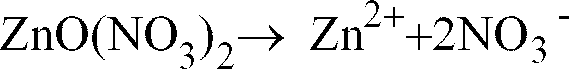


- After washing, the glass substrate will be immersed in a sensitizer liquid containing 1 g/dm-3 of SnCl2 · 2H2O and 1.0 ml/dm-3 of 37 % HCl for several minutes and then will be immersed in an active β liquid containing 0.1 g/dm-3 of PdCl2 and 0.1 ml/dm-3 of 37 % HCl. After having been subjected to the above mentioned preliminary treatment, the said
glass substrate 1 will be immersed in the aqueous solution that is heated to about 50 °C and that contains 0.05 mol/l of zinc nitrate and 0.001 to 0.15 mol/l of dimethylboran (DMAB). Then, after a lapse of time of about 20 minutes, a film ofzinc oxide 20 of a thickness of 0.2 micron will be formed on the saidglass substrate 1. - Unlike a film of zinc oxide that is formed according to a sputtering or electroplating method, a
film 20 that is formed according to the above mentioned method is characterized in that it is high in its insulation properties. This fact constitutes a favorable feature since a high resistivity is required for a zinc oxide material that is used as the base of a black matrix where a color filter is formed by an electroplating method, although a high resistancezinc oxide film 20 that is used as the said transparent electrode is a problem. - An explanation will next be given of a method of forming a color filter and a black matrix without requiring a photo resist at all, with reference to Fig. 17.
- As shown at (a), a said
glass matrix 1 will be formed over its entire surface with a said ITOtransparent electrode 16 by a sputtering or the like technique until its thickness is grown to 500 to 1000 angstroms. In order to polarize and charge the saidtransparent electrode 16, there will be formed thereon atransparent film 25 of a ferroelectric substance (such as PZT) of a thickness of 0.1 micron. Then, the said film of theferroelectric substance 25 will be coated over its entire a zinc oxide material having a photosensitivity by a spin coating or roll coating method and then will be preliminarily baked. Subsequently, by using a black matrix forming mask for a color filter, it will be exposed to a light and developed, whereafter as shown at (b), a film ofzinc oxide 20 mentioned above will be left only in those regions thereof where a black matrix will be formed. Then, by performing a main baking procedure, a fine film ofzinc oxide 20 will be formed. With the said film ofzinc oxide 20 being a film of non-ferroelectric substance, it can be seen that a DC field is applied across it in an attempt to polarize the same, there will be left thereon no residual polarization. Then, as shown at (c), a DC filed will be applied between the saidtransparent electrode 16 poled negative on the saidglass substrate 1 and the positively poled regions where red Rcolor filter elements 3R are to be formed, to produce a residual plus polarization on the surface of the said film of theferroelectric substance 25, as shown at (d). The polarization to this end may be carried out either by polarizing the entire surface of the color filter at a one time with a two-dimensional stylus or successively polarizing the same with a one-dimensional stylus. - Next, the said
glass substrate 1 on which the saidcolor filter elements 3R have been polarized will be immersed in a micell electrolyte in which particles of an organic pigment for a redcolor filter element 3R are dispersed. The said particles of the organic pigment of thecolor filter elements 3R will be charged negative by the presence of a micellized substance so that, as shown at (e), the saidcolor filter elements 3R may be deposited onto the said film of theferroelectric substance 25 whose surface is polarized positive. Similarly, thecolor filter elements 3G and thecolor filter elements 3B will be deposited onto the saidglass substrate 1. In the step (f) shown in Fig. 17, the saidglass substrate 1 on which the saidcolor filter elements copper deposit 23 on each of the portions which are to constitute a black matrix, as shown at (g). Finally, as shown at (h), the surface of the said copper deposit orfilm 23 will be oxidized to form a film of copper oxide 244 thereon. - Fig. 18 illustrates a certain form of embodiment of the method of preparing a cell gap controlling spacer arrangement according to the present invention.
- As shown at (a) in Fig. 18, it is seen that a
black matrix 4 and acolor filter 3 have been formed on a saidglass substrate 1, by using any of the methods mentioned earlier In addition, thecolor filter elements 3 are covered with aprotective film 26. - In such a state, an ITO
thin film 16 constituting the transparent electrode will be formed on the above mentionedprotective film 26 by a sputtering or evaporation method, and a photo resistpattern 27 for the purpose of forming spacers will be formed on the said ITOthin film 16 by using a spacer forming mask. Then, a plurality of squarecolumnar spacers pattern 27 and being connected to the said ITOthin film 16. It can be seen that the top of each of the saidspacers 28 is projected upwards of the said photo resistpattern 27. Then, by using an immersion method, the surface of each of the saidspacers 28 will be coated with a highly insulating film ofzinc oxide 29. - Then, as shown at (b) in Fig. 18, a cell gap controlling
spacer arrangement 28 will result by removing the said photo resistpattern 27. It should be noted at this point that each of the saidspacers 28 may be cylindrical. - And, a liquid crystal display device can be manufactured as shown at (c) in Fig. 18 by attaching a unit with the said
substrate 1 as assembled as above to anothersubstrate 1 with an ITOthin film 16 and so forth with the use of the said cellgap controlling spacers 28 and sealing a liquid crystal in the construction so attached. - According to the present form of embodiment of the invention, it will thus be seen that an arrangement of spacers which are accurately positioned in a photo step without a spacer spreading unit can be prepared to enable a liquid crystal display device to be created with a predetermined thickness.
- While the present invention has hereinbefore been described with respect to a certain illustrative embodiment thereof, it will readily be appreciated by a person skilled in the art to be obvious that many alterations thereof, omissions therefrom and additions thereto can be made without departing from the essence and the scope of the present invention. Accordingly, it should be understood that the present invention is not limited to the specific embodiments thereof set out above, but includes all possible embodiments thereof that can be made within the scope with respect to the features specifically set forth in the appended claims and encompasses all equivalents thereof.
Claims (15)
- A method of manufacturing a color display including a color filter and a black matrix, characterized in that said black matrix is prepared by the steps of:forming a film of zinc oxide on a transparent substrate; andapplying a deposit of electroless copper plating onto said film of zinc oxide while utilizing an catalytic action by palladium chloride, said deposit constituting an element of said black matrix.
- A method of manufacturing a color display including a color filter and a black matrix, characterized in that it comprises the steps of:forming a film of zinc oxide on a transparent substrate;forming said color filter on said film of zinc oxide; andthereafter, applying a deposit of electroless copper plating on an area of said film of zinc oxide on which said color filter is not formed, said deposit having a thickness which is substantially equal to a thickness of said color filter and constituting an element of said black matrix.
- A method as set forth in claim 1 or 2, characterized in that a thin film of copper oxide is formed on a surface of said deposit of electroless plating.
- A method as set forth in any one of claims 1 to 3, characterized in that said film of zinc oxide is doped with aluminum and is then used to serve as a transparent electroplating electrode as well.
- A method as set forth in any one of claims 1 to 4, characterized in that said transparent substrate is a glass substrate.
- A method as set forth in claim 5, characterized in that said glass substrate is made up of a soda glass.
- A method as set forth in any one of claims 1 to 4, characterized in that said transparent substrate is made up of an organic film.
- A method as set forth in claim 7, characterized in that said organic film is a polyester film.
- A method as set forth in any one of claims 1 to 8, characterized in that a driver integrated circuit is connected through a solder bump to said electrolessly plated copper deposit.
- A method of manufacturing a color display including a color filter and a black matrix, characterized in that said color filter is prepared by the steps of:forming a first film that is of a first color filter element of a first color which is selected from three colors: red R, blue B and green G over a surface of a glass substrate, and dividing, by means of eximer laser machining, said first film into a plurality of color filter regions of said first color;forming a second film that is of a second color filter element of a second color which has not been selected from said three colors: R, B and G over such a surface of said glass substrate as is exposed among said first color filter regions of the first color as a result of division of said first film, and dividing, by means of eximer laser machining, said second film into a plurality of color filter regions of said second color; andforming a third film that is of a third color filter element of a third color which has not been selected from said three colors and which is other than said first and second colors, over such a surface of said glass substrate as is exposed among said first and second color filter regions divided from said first and second films, and dividing, by means of eximer laser, said third film into a plurality of color filter regions of said third color,thereby forming over the surface of said substrate a color filter which consists of a plurality of red R color filter elements, a plurality of blue B color filter elements and a plurality of green G color filter elements.
- A method of manufacturing a color display including a color filter and a black matrix, characterized in that said color filter is prepared by the steps of:a) coating a surface of a glass substrate with a transparent electrode;b) forming a transparent film of a ferroelectric substance on said transparent electrode;c) partially polarizing and charging said transparent film of the ferroelectric substance in color filter forming regions thereof of a particular color;d) depositing on said polarized and charged transparent film of the ferroelectric substance a color filter pigment of said particular color that is reversely polarized and charged; ande) repetitively performing the steps c) and d) for said color filter forming regions with respect to a red R, a blue B and a green G color as said particular color.
- A method as set forth in claim 11, characterized in that it comprises the steps of:providing a black matrix forming region in said transparent film of the ferroelectric substance that is formed on said transparent electrode;forming a polarization and charging preventive film on said black matrix forming region;forming an electrolessly plated copper film on said polarization and charging preventive film; andoxidizing at least partially said electrolessly plated copper film.
- A method of manufacturing a color display including a color filter and a black matrix, characterized in that said black matrix is prepared by the steps of:coating a surface of a glass substrate with a transparent electrode;forming a color filter on said transparent electrode;forming on a surface portion of said transparent electrode which has not been formed thereon with said color filter and which is thus exposed a film of zinc oxide with said transparent electrode serving as an electrically conducting terminal;forming an electrolessly plated copper film on said film of zinc oxide; andoxidizing at least partially said electrolessly plated copper film.
- A method of manufacturing a color display including a color filter, a black matrix and a cell gap controlling spacer arrangement, characterized in that said spacer arrangement is prepared by the steps of:forming a glass substrate with a color filter having an uppermost layer constituted of a transparent electrode;forming a photo resist pattern on said transparent electrode while using a mask for forming a spacer;forming a plurality of columnar spacers each composed of transparent zinc oxide by using a solution electrolysis process; andcoating a surface of each of said spacers with an insulating film of zinc oxide.
- A product manufactured by a method as set forth in any one of the preceding claims.
Applications Claiming Priority (6)
| Application Number | Priority Date | Filing Date | Title |
|---|---|---|---|
| JP12155996 | 1996-05-16 | ||
| JP121559/96 | 1996-05-16 | ||
| JP12155996A JP3048221B2 (en) | 1996-05-16 | 1996-05-16 | Black matrix formation method |
| JP10340497 | 1997-04-21 | ||
| JP10340497A JPH10293206A (en) | 1997-04-21 | 1997-04-21 | Formation of color filter, black matrix and spacer for controlling cell gap |
| JP103404/97 | 1997-04-21 |
Publications (2)
| Publication Number | Publication Date |
|---|---|
| EP0807846A2 true EP0807846A2 (en) | 1997-11-19 |
| EP0807846A3 EP0807846A3 (en) | 2000-03-01 |
Family
ID=26444041
Family Applications (1)
| Application Number | Title | Priority Date | Filing Date |
|---|---|---|---|
| EP97303293A Withdrawn EP0807846A3 (en) | 1996-05-16 | 1997-05-14 | Color Display and its manufacturing method |
Country Status (2)
| Country | Link |
|---|---|
| US (2) | US6208404B1 (en) |
| EP (1) | EP0807846A3 (en) |
Cited By (5)
| Publication number | Priority date | Publication date | Assignee | Title |
|---|---|---|---|---|
| WO2007118895A1 (en) * | 2006-04-19 | 2007-10-25 | Commissariat A L'energie Atomique | Microstructured spectral filter and image sensor |
| EP1163544B1 (en) * | 1999-03-17 | 2010-12-29 | SABIC Innovative Plastics IP B.V. | method of making ultraviolet filters with enhanced weatherability |
| US9122007B2 (en) | 2008-09-11 | 2015-09-01 | Commissariat A L'energie Atomique Et Aux Energies Alternatives | Nanostructured spectral filter and image sensor |
| US9236157B2 (en) | 2009-09-03 | 2016-01-12 | Isis Innovation Limited | Transparent electrically conducting oxides |
| US9552902B2 (en) | 2008-02-28 | 2017-01-24 | Oxford University Innovation Limited | Transparent conducting oxides |
Families Citing this family (10)
| Publication number | Priority date | Publication date | Assignee | Title |
|---|---|---|---|---|
| US6410214B1 (en) * | 1998-10-01 | 2002-06-25 | Lg Electronics Inc. | Method for manufacturing black matrix of plasma display panel |
| KR100301667B1 (en) * | 1999-05-21 | 2001-09-26 | 구본준, 론 위라하디락사 | Liquid Crystal Display Device And Fabricating Method Thereof |
| JP2001266654A (en) * | 2000-01-11 | 2001-09-28 | Sanyo Electric Co Ltd | Transparent electrode and its patterning method and method of manufacturing semiconductor element using the same |
| JP2002033058A (en) * | 2000-07-14 | 2002-01-31 | Sony Corp | Front plate for field emission type display device |
| US20020061510A1 (en) * | 2000-10-16 | 2002-05-23 | Jonathan Miller | Method and system for designing proteins and protein backbone configurations |
| KR101002648B1 (en) * | 2003-11-26 | 2010-12-20 | 삼성에스디아이 주식회사 | Flat panel display device and method of preparing the same |
| US20060215105A1 (en) * | 2005-03-28 | 2006-09-28 | Innolux Display Corp. | Liquid crystal display device with photo spacers |
| KR101182305B1 (en) * | 2005-06-30 | 2012-09-20 | 엘지디스플레이 주식회사 | A method for fabricating the same |
| CN101295090B (en) * | 2007-04-27 | 2010-12-29 | 群康科技(深圳)有限公司 | LCD device |
| US20110254440A1 (en) * | 2009-01-07 | 2011-10-20 | Kiyoshi Minoura | Organic electroluminescence display device and method for producing the same |
Citations (11)
| Publication number | Priority date | Publication date | Assignee | Title |
|---|---|---|---|---|
| US4787716A (en) * | 1984-02-28 | 1988-11-29 | Seiko Instruments & Electronics Ltd. | Color member and method for manufacturing same |
| US4818075A (en) * | 1987-01-23 | 1989-04-04 | Canon Kabushiki Kaisha | Color liquid crystal device |
| EP0431249A2 (en) * | 1989-12-08 | 1991-06-12 | International Business Machines Corporation | Electrostatic deposition of LCD color filters |
| US5117299A (en) * | 1989-05-20 | 1992-05-26 | Ricoh Company, Ltd. | Liquid crystal display with a light blocking film of hard carbon |
| EP0572672A1 (en) * | 1991-10-02 | 1993-12-08 | Nippon Paint Co., Ltd. | Process for manufacturing multicolor display |
| US5340619A (en) * | 1993-10-18 | 1994-08-23 | Brewer Science, Inc. | Method of manufacturing a color filter array |
| US5401616A (en) * | 1992-09-21 | 1995-03-28 | Matsushita Electric Industrial Co., Ltd. | Patterning method employing laser |
| EP0670509A1 (en) * | 1994-03-01 | 1995-09-06 | Seiko Instruments Inc. | Method for manufacturing colour filter and multiple colour liquid crystal display devices |
| EP0675383A1 (en) * | 1994-03-28 | 1995-10-04 | Nippon Paint Co., Ltd. | Method for correcting defect in color filter |
| EP0725303A1 (en) * | 1995-02-06 | 1996-08-07 | International Business Machines Corporation | Liquid crystal display device |
| EP0772071A1 (en) * | 1995-11-06 | 1997-05-07 | Sharp Kabushiki Kaisha | Liquid crystal display element and fabrication process thereof |
Family Cites Families (2)
| Publication number | Priority date | Publication date | Assignee | Title |
|---|---|---|---|---|
| FR2697922B1 (en) * | 1992-11-12 | 1995-09-22 | Gold Star Co | METHOD FOR MANUFACTURING A COLOR FILTER FOR A LIQUID CRYSTAL SCREEN. |
| JPH09152507A (en) * | 1995-03-29 | 1997-06-10 | Seiko Instr Inc | Production of multicolor liquid crystal display device |
-
1997
- 1997-05-13 US US08/854,897 patent/US6208404B1/en not_active Expired - Fee Related
- 1997-05-14 EP EP97303293A patent/EP0807846A3/en not_active Withdrawn
-
2000
- 2000-12-20 US US09/747,390 patent/US20010001288A1/en not_active Abandoned
Patent Citations (11)
| Publication number | Priority date | Publication date | Assignee | Title |
|---|---|---|---|---|
| US4787716A (en) * | 1984-02-28 | 1988-11-29 | Seiko Instruments & Electronics Ltd. | Color member and method for manufacturing same |
| US4818075A (en) * | 1987-01-23 | 1989-04-04 | Canon Kabushiki Kaisha | Color liquid crystal device |
| US5117299A (en) * | 1989-05-20 | 1992-05-26 | Ricoh Company, Ltd. | Liquid crystal display with a light blocking film of hard carbon |
| EP0431249A2 (en) * | 1989-12-08 | 1991-06-12 | International Business Machines Corporation | Electrostatic deposition of LCD color filters |
| EP0572672A1 (en) * | 1991-10-02 | 1993-12-08 | Nippon Paint Co., Ltd. | Process for manufacturing multicolor display |
| US5401616A (en) * | 1992-09-21 | 1995-03-28 | Matsushita Electric Industrial Co., Ltd. | Patterning method employing laser |
| US5340619A (en) * | 1993-10-18 | 1994-08-23 | Brewer Science, Inc. | Method of manufacturing a color filter array |
| EP0670509A1 (en) * | 1994-03-01 | 1995-09-06 | Seiko Instruments Inc. | Method for manufacturing colour filter and multiple colour liquid crystal display devices |
| EP0675383A1 (en) * | 1994-03-28 | 1995-10-04 | Nippon Paint Co., Ltd. | Method for correcting defect in color filter |
| EP0725303A1 (en) * | 1995-02-06 | 1996-08-07 | International Business Machines Corporation | Liquid crystal display device |
| EP0772071A1 (en) * | 1995-11-06 | 1997-05-07 | Sharp Kabushiki Kaisha | Liquid crystal display element and fabrication process thereof |
Non-Patent Citations (1)
| Title |
|---|
| MURPHY M: "Method for Manufacturing a Color Filter" METAL FINISHING,US,ELSEVIER SCIENCE PUBLISHING, NEW YORK, NY, vol. 96, no. 5, page 92 XP004118343 ISSN: 0026-0576 * |
Cited By (6)
| Publication number | Priority date | Publication date | Assignee | Title |
|---|---|---|---|---|
| EP1163544B1 (en) * | 1999-03-17 | 2010-12-29 | SABIC Innovative Plastics IP B.V. | method of making ultraviolet filters with enhanced weatherability |
| WO2007118895A1 (en) * | 2006-04-19 | 2007-10-25 | Commissariat A L'energie Atomique | Microstructured spectral filter and image sensor |
| FR2900279A1 (en) * | 2006-04-19 | 2007-10-26 | Commissariat Energie Atomique | MICRO-STRUCTURE SPECTRAL FILTER AND IMAGE SENSOR |
| US9552902B2 (en) | 2008-02-28 | 2017-01-24 | Oxford University Innovation Limited | Transparent conducting oxides |
| US9122007B2 (en) | 2008-09-11 | 2015-09-01 | Commissariat A L'energie Atomique Et Aux Energies Alternatives | Nanostructured spectral filter and image sensor |
| US9236157B2 (en) | 2009-09-03 | 2016-01-12 | Isis Innovation Limited | Transparent electrically conducting oxides |
Also Published As
| Publication number | Publication date |
|---|---|
| US20010001288A1 (en) | 2001-05-17 |
| EP0807846A3 (en) | 2000-03-01 |
| US6208404B1 (en) | 2001-03-27 |
Similar Documents
| Publication | Publication Date | Title |
|---|---|---|
| US6208404B1 (en) | Black matrix | |
| US4422731A (en) | Display unit with half-stud, spacer, connection layer and method of manufacturing | |
| US7052811B2 (en) | Color filter, display device and electronic equipment, manufacturing method thereof, and apparatus for manufacturing display device | |
| US8665401B2 (en) | Liquid crystal display panel having hydrophobic planarization with hydrophilic regions and fabricating method and apparatus thereof | |
| JPH10142610A (en) | Liquid crystal device and its manufacture | |
| KR20050059154A (en) | Tft array substrate, liquid crystal display device, manufacturing methods of tft array substrate and liquid crystal display device, and electronic device | |
| JPH1062789A (en) | Liquid crystal display device and its production | |
| CN101149506B (en) | Liquid crystal display panel manufacturing method and liquid crystal display panel | |
| DE602006000191T2 (en) | Pixel electrode, process for its manufacture, electro-optical device and electronic device | |
| KR100411570B1 (en) | Method for manufacturing multicolor liquid crystal display device | |
| JP2000098368A (en) | Active matrix substrate and its manufacture, liquid crystal display device using the same | |
| JPH10186349A (en) | Liquid crystal display element and production thereof | |
| JP4970242B2 (en) | Application of color elements and bus bars to display substrates | |
| JP4689943B2 (en) | Electrochromic display device and manufacturing method thereof | |
| CN100456099C (en) | Liquid crystal display device | |
| US5702871A (en) | Liquid crystal display with low resistance electrode and method therefor | |
| KR20010067098A (en) | Method for fabricating metal wirings | |
| KR960013793B1 (en) | Color filter and production thereof | |
| JPS6212899B2 (en) | ||
| US5595790A (en) | Method for forming a reflective surface for a LCD | |
| JP3552805B2 (en) | Method of manufacturing film liquid crystal panel | |
| JPH11259008A (en) | Planar panel display device provided with patterned conductive trace of internal connection type | |
| JPH10293206A (en) | Formation of color filter, black matrix and spacer for controlling cell gap | |
| JPH01138530A (en) | Manufacture of color display device | |
| JPS63144390A (en) | Manufacture of display device |
Legal Events
| Date | Code | Title | Description |
|---|---|---|---|
| PUAI | Public reference made under article 153(3) epc to a published international application that has entered the european phase |
Free format text: ORIGINAL CODE: 0009012 |
|
| AK | Designated contracting states |
Kind code of ref document: A2 Designated state(s): DE FR GB IT |
|
| PUAL | Search report despatched |
Free format text: ORIGINAL CODE: 0009013 |
|
| AK | Designated contracting states |
Kind code of ref document: A3 Designated state(s): DE FR GB IT |
|
| 17P | Request for examination filed |
Effective date: 20000829 |
|
| STAA | Information on the status of an ep patent application or granted ep patent |
Free format text: STATUS: THE APPLICATION HAS BEEN WITHDRAWN |
|
| 18W | Application withdrawn |
Withdrawal date: 20010419 |