EP0806867A2 - Video signal processing apparatus - Google Patents
Video signal processing apparatus Download PDFInfo
- Publication number
- EP0806867A2 EP0806867A2 EP97107508A EP97107508A EP0806867A2 EP 0806867 A2 EP0806867 A2 EP 0806867A2 EP 97107508 A EP97107508 A EP 97107508A EP 97107508 A EP97107508 A EP 97107508A EP 0806867 A2 EP0806867 A2 EP 0806867A2
- Authority
- EP
- European Patent Office
- Prior art keywords
- signal
- video signal
- synchronizing
- programmable
- video
- Prior art date
- Legal status (The legal status is an assumption and is not a legal conclusion. Google has not performed a legal analysis and makes no representation as to the accuracy of the status listed.)
- Granted
Links
Images


Classifications
-
- H—ELECTRICITY
- H04—ELECTRIC COMMUNICATION TECHNIQUE
- H04N—PICTORIAL COMMUNICATION, e.g. TELEVISION
- H04N5/00—Details of television systems
- H04N5/44—Receiver circuitry for the reception of television signals according to analogue transmission standards
- H04N5/46—Receiver circuitry for the reception of television signals according to analogue transmission standards for receiving on more than one standard at will
Definitions
- the present invention relates to the field of video signal processing apparatus which regenerates and decodes video signals employing a programmable signal processor.
- NTSC broadcasting systems via broadcast satellite and communications satellite, high definition television broadcasting, and digital television broadcasting are already in operation, in addition to existing terrestrial television broadcasting in NTSC color format (hereafter referred to as NTSC television broadcasting).
- VGA-class Video Graphics Array
- Fig. 6 shows a block diagram of a television set designed to receive both NTSC television composite video signals and MUSE television composite video signals.
- NTSC television composite video signals are received as follows.
- a tuner selects a channel for NTSC television composite video signals. Signals are amplified by a VIF (Video Intermediate Frequency) amplifier and then detected by a detector to generate baseband NTSC TV composite video signals. Baseband NTSC TV composite video signals are input to an input terminal 72 in Fig. 6.
- a clamping circuit 82 adjusts the DC level of the baseband NTSC television composite video signals to an appropriate level, and an analog-to-digital converter 83 quantizes the resultant baseband NTSC television composite video signals and converts them to digital signals.
- Sampling frequency for quantization is phase-locked to the color subcarrier and has a four times (hereafter referred to as 4f sc ) higher frequency than the color subcarrier: approximately 14 MHz.
- Digitized baseband NTSC TV composite video signals are fed to a NTSC video signal decoder 76N.
- a synchronizing signal regenerator 75 for NTSC TV composite video signals regenerates a clock signal ⁇ 81 , phase-locked to the color subcarrier, from quantized and digitized baseband NTSC TV composite video signals with a resonance circuit comprising a crystal resonator 102.
- the synchronizing signal regenerator 75 also detects synchronizing signal components of quantized and digitized NTSC composite video signals with the clock signal ⁇ 81 , regenerates horizontal synchronizing signals and vertical synchronizing signals, and generates the required pulse signals such as a clock signal ⁇ 82 phase-locked to input horizontal synchronizing signals and a clamp pulse.
- the NTSC TV composite video signal decoder 76N decodes NTSC TV composite video signals through a luminance signal process and a chrominance signal process using a range of signals including clock signal ⁇ 81 , clock signal ⁇ 82 , and horizontal synchronizing signals.
- the 2nd phase extended definition television standard (ED2) baseband composite video signal decoder 76E regenerates horizontal high-emphasis processing signals from ED2 composite video signals, in addition to decoding by 76N, using the clock signals ⁇ 81 , clock signals phased-locked to ⁇ 81 , and synchronizing signals.
- Video signals after the above processing are sampled by a clock signal ⁇ 83 synchronized with the horizontal synchronizing pulse and vertical synchronizing pulse of the output circuit for synchronizing video signals with the horizontal synchronizing pulse and vertical synchronizing pulse of the output circuit.
- the clock signal ⁇ 83 is generated from a resonance circuit comprising a crystal resonator 103, and is synchronized with the horizontal synchronizing pulse and vertical synchronizing pulse of the output circuit.
- a vertical high-emphasis processing signal is regenerated using the clock signal ⁇ 83 and a clock signal phase-locked to ⁇ 83 .
- the luminance signal process in 76N and the luminance signal process in 76E can be combined to share a common circuit, as can the chrominance signal process in 76N and the chrominance signal process in 76E .
- the method for decoding MUSE television composite video signals is as follows.
- a tuner selects a channel, and the VIF (video intermediate frequency) circuit amplifies the signals received.
- the detector detects the waveform and generates baseband MUSE television composite video signals.
- Baseband MUSE TV composite video signals are input to an input terminal 71.
- a clamping circuit 92 adjusts the DC level of baseband MUSE television composite video signals to appropriate level, and an analog-to-digital converter 93 quantizes baseband MUSE television composite video signals and converts them to digital composite video signals.
- a clock signal which is phase-locked to the horizontal phase standard signal and is about 16.2 MHz is used as sampling frequency for quantization.
- Digitized MUSE TV composite video signals are fed to a MUSE TV composite video signal decoder 74.
- the decoder 74 regenerates wide-band high definition video signals by approximately interpolating untransmitted signals of sampling points employing infield interpolation, inframe interpolation, or interframe interpolation.
- a synchronizing signal regenerator 73 for MUSE television composite video signals regenerates horizontal phase standard signals, horizontal synchronizing signals, vertical phase standard signals, and vertical synchronizing signals from MUSE composite video signals.
- the synchronizing signal regenerator 73 regenerates a clock signal ⁇ 91 required for operating the MUSE composite video signal decoder, from a resonance circuit comprising a crystal resonator 100, and generates a range of control signals for the input signal.
- video signals of horizontal scanning period are compressed to 11/12 for transmission, requiring the decoder to decompress them.
- a clock signal ⁇ 93 phase-locked to the horizontal scanning pulse of the display apparatus, whose frequency is about 44 MHz, is generated from the resonance circuit comprising the crystal resonator 101.
- decoded video signals are sampled by the clock signal ⁇ 93 of about 44 MHz, and synchronized with the horizontal scanning pulse.
- the digital-to-analog converters 87 and 97 convert each of the outputs of the NTSC television composite video signal decoder 76N, the ED2 composite video signal decoder 76E, and the MUSE television composite video signal decoder 74 to analog signals.
- the switching circuit 80 selects and outputs signals.
- the switching circuit 79 also selects and outputs synchronizing signals.
- the present invention relates to a video signal processing apparatus for regenerating and decoding video signals employing programmable signal processors.
- the object of the present invention is to provide solutions to the above disadvantages.
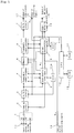
- Fig. 1 is a block diagram of a video signal processing apparatus of the present invention.
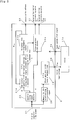
- Fig. 2 is a block diagram of an input synchronizing signal processor of the video signal processing apparatus in Fig.1.
- Fig. 3 is a block diagram of an output synchronizing signal processor of the video signal processing apparatus in Fig. 1.
- Fig. 4 is a block diagram of an output deflection signal generator of the video signal processing apparatus in Fig. 1.
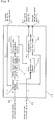
- Fig. 5 is a block diagram of a programmable signal processor of the video signal processing apparatus in Fig. 1.
- Fig. 6 is a block diagram of the conventional video signal processing apparatus for receiving and processing the NTSC television composite video signal and the MUSE television composite video signal.
- Fig. 1 is a block diagram of a video signal processing apparatus of the present invention.
- the invention is intended for a wide range of input composite video signals (including synchronizing signals) such as MUSE TV composite video signals, NTSC TV composite video signals, and high definition baseband TV composite signals.
- a signal selector 1 selects a video signal
- a clamping circuit 2 adjusts the DC level
- an analog-to-digital converter 3 converts the video signal to a digital video signal.
- the digital video signal is then supplied to a first programmable signal processor 4 and an input synchronizing signal processor 8.
- the input synchronizing signal processor 8 separates and regenerates the synchronizing signal from the input video signal and also generates a clock signal phase-locked to the horizontal phase standard signal of the input video signal.
- Fig. 2 is a block diagram of the input synchronizing signal processor 8.
- the input synchronizing signal processor 8 comprises a programmable counter in order to process multiple input composite video signals.
- Such processor can be provided with a structure to switch functions and operations of each block according to multiple input composite video signals.
- a synchronizing signal detector 20 separates the horizontal synchronizing signal component and vertical synchronizing signal component from the digital video signal.
- the DC level of the synchronizing signal is specified to be lower than the black level of the video signal. Therefore, horizontal and vertical synchronizing signal components are separable by integrating the output after slicing based on the appropriate slice level setting in a synchronizing signal separator.
- a frame synchronizing pulse which is the vertical synchronizing signal component, is detectable by autocorrelation with time.
- the horizontal synchronizing signal component is separable by a counter activated by said frame synchronizing pulse.
- a digital composite video signal is input to the memory 25 for the synchronizing standard signal.
- the memory 25 extracts the waveform of the horizontal phase standard signal mixed in the composite video signal.
- the memory extracts a color burst signal for regenerating color subcarrier.
- the extracted digital signal waveform is sent to a CPU 12. Via the operation of a loop filter, the input voltage V 28 to be applied to the input voltage terminal 28 of a VCO is calculated by the CPU and supplied to a VCO 11a to form a feedback loop.
- the VCO 11a is a wideband variable clock generator controlled by DC voltage, and is capable of generating a wideband clock pulse, for example, about 32 MHz for MUSE TV composite video signals, 28 MHz for NTSC TV composite video signals, and 50 MHz for VGA (Video Graphics Array) employing, for example, a positive feedback oscillator as an oscillation source.
- a wideband clock pulse for example, about 32 MHz for MUSE TV composite video signals, 28 MHz for NTSC TV composite video signals, and 50 MHz for VGA (Video Graphics Array) employing, for example, a positive feedback oscillator as an oscillation source.
- the output clock pulse ⁇ 29 of the VCO 11a is sent to the analog-to-digital converter 3, the programmable processor 4, and the input synchronizing signal processor 8, and used as a system clock pulse.
- the output horizontal synchronizing pulse from the synchronizing signal detector 20 is not used as it is, and requires to be stabilized using a feedback loop in order to process non-standard NTSC composite video signals such as reconstruction signals of the VTR.
- a horizontal synchronizing phase detector 21a detects any phase error between the generated horizontal synchronizing pulse and the horizontal synchronizing signal detected by the horizontal synchronizing phase detector 21a.
- the detection result is sent to the CPU 12 for calculating the dividing ratio to be used for a horizontal rate programmable counter 23a to cancel the phase error.
- the CPU 12 sends the calculation result to the horizontal rate programmable counter 23a to form a feedback loop. Said calculation result indicates the number of input system clock pulses in one horizontal scanning period.
- the divided output of said horizontal rate programmable counter 23 is sent to a memory 5 as a write address. Any phase error below the cycle frequency of the system clock is detected by the CPU 12 as a horizontal skew, and such phase error can be absorbed by applying a phase correction which cancels the skew in the programmable processor 4.
- the pulse generating counter 24a adjusts the divided output of the horizontal rate programmable counter 23a to the required phase and pulse width, and sends it to an output synchronizing pulse processor 9 as a detected horizontal synchronizing pulse ⁇ 31 .
- the pulse generating counter 24a also adjusts the vertical synchronizing signal detected by the synchronizing signal detector 20 in Fig. 20 to the required phase and pulse width, and outputs it as a detected vertical synchronizing pulse ⁇ 32 .
- FIG. 5 is a preferred embodiment of a block diagram of the programmable processor.
- a processing element 50 is aligned in matrix based on MIMD (Multiple Instruction Multiple Data stream) system, and each processing element 50 is connected by lattice network wiring.
- the processing element 50 comprises an arithmetic and logic unit (ALU), an instruction register which controls the ALU, and a data register for inputting numerical values.
- ALU arithmetic and logic unit
- Each register is connected to the CPU 12 by an exclusive wire so that methods of signal processing are dynamically changeable by rewriting the register according to the standard of input video signal or type of decode mode.
- Table 1 is a comparison between the signal process of programmable signal processors and each signal format.
- the programmable signal processor 4 separates Y/C, decodes the chrominance signal, and processes ACC for decoding NTSC TV composite video signals.
- the programmable signal processor 4 For decoding ED2 TV composite video signals, the programmable signal processor 4 separates Y/C, decodes the chrominance signal, processes ACC, and processes the horizontal high-emphasis signal (HH).
- the input system clock pulses ⁇ 29 are used for these processes.
- the programmable signal processor 4 interpolates the still picture region and moving picture region of the signal, detects motion, and processes progressive scanning.
- Signals decoded with the programmable signal processor 4 are written into the memory 5 for synchronizing with the system clock pulse for display.
- a readable/writable memory (so-called read modified write) is used for sending and receiving digital signals between circuits operated by different system clock signals.
- the write address for the memory 5 is formed by the input system clock pulse ⁇ 29 generated from the input synchronizing signal processor 8 which generates an input synchronizing signal and a range of pulses synchronized to it.
- Table 1 NTSC TV composite video signal Decoding ED2 TV composite video signal Decoding MUSE TV composite video signal Decoding Programmable signal processor 4 YE separation YE separation Interpolation in still picture region Chrominance signal decoding Chrominance signal decoding Interpolation in moving picture region ACC process ACC process Motion detection HH regeneration Progressive scanning process Programmable signal processor 6 Line signal interpolation Line signal interpolation Picture quality compensation VT/VH regeneration Caption signal insertion Caption signal insertion Picture quality compensation
- the horizontal synchronizing signal ⁇ 31 , vertical synchronizing signal ⁇ 32 and external synchronizing signal ⁇ 16 detected by the input synchronizing signal processor 8 form the phase-locked loop (PLL) for synchronizing the system clock for display to the external synchronizing signal ⁇ 16 .
- PLL phase-locked loop
- the external synchronizing signal ⁇ 16 uses the synchronizing signal of the video signal to be displayed in the main picture as the standard of the synchronizing pulse for display, and generate an address data, based on the standard, for storing the video signal to be displayed in the sub-picture in the memory 5.
- Fig. 2 and Fig. 3 omit signal processing of the external synchronizing signal, but the memory 5 can be synchronized to the external synchronizing signal just by switching over the write address.
- a write address generator is operated by field periodically, when inputting the external synchronizing signal, to absorb the difference in frame frequency. When inputting the internal synchronizing signal, the write address generator is operated by frame periodically.
- the picture-in-picture display is realized by writing two types of asynchronous digital video signals to the memory using the external synchronizing signal ⁇ 16 , the input system clock pulse ⁇ 69 synchronized to the signal ⁇ 16 , and the internal input system clock pulse ⁇ 29 , and reading out the digital video signal from the memory 5 using the same system clock pulses for display.
- a horizontal phase detector 21b detects any phase error between the horizontal synchronizing pulse ⁇ 34 generated from a horizontal rate programmable counter 23b, which divides the approximately 28-MHz clock to 1/1820, and the detected horizontal synchronizing pulse ⁇ 31 .
- the detection result is calculated with the CPU 12 to convert the result to voltage, and it is output as V28 from the input voltage terminal 28 to control the oscillation frequency of a VCO 11b.
- the VCO 11b adds the output system clock ⁇ 33 , synchronized to the horizontal scanning frequency of display apparatus, to the horizontal programmable counter 23b to form a feedback loop.
- the synchronizing pulse processor for display apparatus 9 always operates with reference to the output system clock ⁇ 33 as a standard clock.
- the time constant of said feedback loop is set very long to form a stable output system clock locked to the line frequency of the input video signal and to avoid the influence of jitters from the input horizontal synchronizing signal.
- the horizontal rate programmable counter 23b which is controlled by the horizontal synchronizing pulse adjusts the output horizontal scanning rate pulse to the required phase and pulse width using a pulse generator with counter 24b, and outputs the pulse as a horizontal synchronizing pulse ⁇ 35 for display.
- the pulse generator with counter 24b adjusts the phase and pulse width of the detected vertical synchronizing pulse and outputs it as a vertical synchronizing pulse ⁇ 36 .
- the frequency of the system clock signal ⁇ 33 for display is approximately 44 MHz and the dividing ratio used in the horizontal rate programmable counter 23b controlled by the horizontal synchronizing pulse is 1/1320.
- the VCO 11a and VCO 11b are variable oscillators adjustable from about 10 MHz to 50 MHz in order to correspond to wideband output signals.
- the read-out address of the memory 5 is created in the output synchronizing pulse processor 9.
- the line memory is used to process video signals by line and convert read-out phase and frequency using the output system clock ⁇ 33 .
- the programmable signal processor 6 decodes the composite video signal using the output system clock ⁇ 33 and the output synchronizing pulse. As shown in Table 1, for decoding NTSC TV composite video signals, processes including line signal interpolation, caption signal insertion, and picture quality compensation are executed. For decoding ED2 signals, processes including line signal interpolation, regeneration of vertical temporal-emphasis processing signal (VT) or vertical high-emphasis processing signal (VH), caption signal insertion, and picture quality compensation are executed.
- VT vertical temporal-emphasis processing signal
- VH vertical high-emphasis processing signal
- ROM Read Only Memory
- the CPU 12 loads the required program for decoding video signals into the instruction register of the programmable signal processor depending on the type of video signal detected.
- Decoded composite video signals are converted to analog signals via the digital-to-analog converter 7, and output as video signals for display.
- the output synchronizing pulse processor 9 generates a synchronizing pulse ⁇ 18 which is shaped to the pulse waveform.
- Fig. 4 illustrates a deflection signal generator 10.
- the pulses driving the horizontal output transistor are fed back to a horizontal phase detector 21c and form a PLL circuit comprising the horizontal synchronizing pulse to stabilize the special operation of the horizontal deflection circuit for CRT.
- the horizontal phase detector 21c detects any frequency or phase errors between the output horizontal synchronizing pulse ⁇ 35 and the pulses driving the horizontal output transistor ⁇ 41 for deflection.
- the detection result is input to the CPU 12, which contains a horizontal scanning signal processor which forms a feedback loop to calculate any phase error.
- the value to compensate for the calculated phase error is set as the dividing ratio to a horizontal rate programmable counter 23c.
- the pulse generator with counter 24c adjusts the phase and pulse width of the output of the horizontal rate programmable counter 23c. Since the above processes are executed in a unit of the system clock for display, any phase error below the clock rate of the system clock for display ⁇ 33 is ignored. (In other words, the system does not respond to such phase error.)
- a compensation circuit to the skew of clock signal 40 compensates continuously, in analog, the phase error calculated by the horizontal synchronizing signal processor forming a feedback loop in the CPU 12, amplifies the pulse waveform of the generated horizontal frequency, and outputs it as the horizontal deflection output pulse ⁇ 42 .
- the pulse generator with counter 24c shapes the waveform of the vertical synchronizing output pulse ⁇ 36 and outputs it as the vertical deflection output pulse ⁇ 43 . Depend on the horizontal deflection output pulse ⁇ 42 and the vertical deflection output pulse ⁇ 43 .
- the present invention has programmable signal processors connected to the input terminal and the output terminal of the memory, thereby enabling one video signal processor to process video signals of many different broadcasting systems which have different synchronizing signal frequencies, field frequencies, and sampling frequencies, and data signals composed of composite synchronizing signals which have different sampling frequencies.
Abstract
Description
- The present invention relates to the field of video signal processing apparatus which regenerates and decodes video signals employing a programmable signal processor.
- The specifications of broadcasting system for television signals are becoming increasingly diverse. At present, NTSC broadcasting systems via broadcast satellite and communications satellite, high definition television broadcasting, and digital television broadcasting are already in operation, in addition to existing terrestrial television broadcasting in NTSC color format (hereafter referred to as NTSC television broadcasting).
- As the specifications of broadcasting systems continue to diversify, television sets require the corresponding ability to receive television signals broadcast via a range of broadcasting systems. In addition, as information processing devices such as personal computers become increasingly popular, display performance of so-called VGA-class (Video Graphics Array) resolution is required for home-use television sets.
- Conventionally, television signals from different broadcasting systems are received and processed by switching field frequency, resolution, and number of horizontal scanning lines for each system, and this has resulted in larger and more complicated circuits.
- For example, Fig. 6 shows a block diagram of a television set designed to receive both NTSC television composite video signals and MUSE television composite video signals.
- NTSC television composite video signals are received as follows. A tuner selects a channel for NTSC television composite video signals. Signals are amplified by a VIF (Video Intermediate Frequency) amplifier and then detected by a detector to generate baseband NTSC TV composite video signals. Baseband NTSC TV composite video signals are input to an
input terminal 72 in Fig. 6. A clamping circuit 82 adjusts the DC level of the baseband NTSC television composite video signals to an appropriate level, and an analog-to-digital converter 83 quantizes the resultant baseband NTSC television composite video signals and converts them to digital signals. Sampling frequency for quantization is phase-locked to the color subcarrier and has a four times (hereafter referred to as 4fsc) higher frequency than the color subcarrier: approximately 14 MHz. Digitized baseband NTSC TV composite video signals are fed to a NTSC video signal decoder 76N. - On the other hand, a synchronizing signal regenerator 75 for NTSC TV composite video signals regenerates a clock signal φ81, phase-locked to the color subcarrier, from quantized and digitized baseband NTSC TV composite video signals with a resonance circuit comprising a
crystal resonator 102. The synchronizing signal regenerator 75 also detects synchronizing signal components of quantized and digitized NTSC composite video signals with the clock signal φ81, regenerates horizontal synchronizing signals and vertical synchronizing signals, and generates the required pulse signals such as a clock signal φ82 phase-locked to input horizontal synchronizing signals and a clamp pulse. The NTSC TV composite video signal decoder 76N decodes NTSC TV composite video signals through a luminance signal process and a chrominance signal process using a range of signals including clock signal φ81, clock signal φ82, and horizontal synchronizing signals. - The 2nd phase extended definition television standard (ED2) baseband composite video signal decoder 76E regenerates horizontal high-emphasis processing signals from ED2 composite video signals, in addition to decoding by 76N, using the clock signals φ81, clock signals phased-locked to φ81, and synchronizing signals. Video signals after the above processing are sampled by a clock signal φ83 synchronized with the horizontal synchronizing pulse and vertical synchronizing pulse of the output circuit for synchronizing video signals with the horizontal synchronizing pulse and vertical synchronizing pulse of the output circuit. The clock signal φ83 is generated from a resonance circuit comprising a crystal resonator 103, and is synchronized with the horizontal synchronizing pulse and vertical synchronizing pulse of the output circuit. For ED2 composite video signals, after the abovementioned processing, a vertical high-emphasis processing signal is regenerated using the clock signal φ83 and a clock signal phase-locked to φ83.
- At this point, the luminance signal process in 76N and the luminance signal process in 76E can be combined to share a common circuit, as can the chrominance signal process in 76N and the chrominance signal process in 76E .
- The method for decoding MUSE television composite video signals is as follows. A tuner selects a channel, and the VIF (video intermediate frequency) circuit amplifies the signals received. The detector detects the waveform and generates baseband MUSE television composite video signals. Baseband MUSE TV composite video signals are input to an
input terminal 71. Aclamping circuit 92 adjusts the DC level of baseband MUSE television composite video signals to appropriate level, and an analog-to-digital converter 93 quantizes baseband MUSE television composite video signals and converts them to digital composite video signals. A clock signal which is phase-locked to the horizontal phase standard signal and is about 16.2 MHz is used as sampling frequency for quantization. Digitized MUSE TV composite video signals are fed to a MUSE TV compositevideo signal decoder 74. Thedecoder 74 regenerates wide-band high definition video signals by approximately interpolating untransmitted signals of sampling points employing infield interpolation, inframe interpolation, or interframe interpolation. - A synchronizing
signal regenerator 73 for MUSE television composite video signals regenerates horizontal phase standard signals, horizontal synchronizing signals, vertical phase standard signals, and vertical synchronizing signals from MUSE composite video signals. In addition, thesynchronizing signal regenerator 73 regenerates a clock signal φ91 required for operating the MUSE composite video signal decoder, from a resonance circuit comprising acrystal resonator 100, and generates a range of control signals for the input signal. Moreover, for MUSE composite video signals, video signals of horizontal scanning period are compressed to 11/12 for transmission, requiring the decoder to decompress them. For this purpose, a clock signal φ93, phase-locked to the horizontal scanning pulse of the display apparatus, whose frequency is about 44 MHz, is generated from the resonance circuit comprising the crystal resonator 101. At the final stage of decoding process for MUSE composite video signals, decoded video signals are sampled by the clock signal φ93 of about 44 MHz, and synchronized with the horizontal scanning pulse. The digital-to-analog converters video signal decoder 74 to analog signals. The switching circuit 80 selects and outputs signals. At the same time, theswitching circuit 79 also selects and outputs synchronizing signals. - The present invention relates to a video signal processing apparatus for regenerating and decoding video signals employing programmable signal processors.
- In general, an exclusive decoder, synchronizing regenerator, and clock generator are required for decoding input television video signals of each signal standard. This has resulted in larger circuits and also disadvantages in cost and productivity.
- The object of the present invention is to provide solutions to the above disadvantages.
- (1) The present invention relates to a video signal processing apparatus employing a synchronizing signal processor for separating and processing the synchronizing signal from the composite video signal, a clock signal generator for generating the clock signal phase-locked to the horizontal phase standard signal in the video signal, a first programmable signal processor for decoding the video signal, a storage means for storing the output signal of the first programmable signal processor, a generating and processing means of the output synchronizing pulse for generating and processing the synchronizing pulse so as to display the video signal on the display apparatus, a memory for storing multiple programs which are used for processing the video signal after the first decoding step by said first programmable signal processor at receiving the output signal from said storage, and a control means for selecting and reading out a suitable program from the memory where the multiple programs are stored.
The present invention enables one video display apparatus to process signals with different formats by overwriting an operating program of the programmable signal processor depending on the format of the input composite video signal, and thus provides cost-efficient video signal processing apparatus with higher productivity. - (2) The present invention also relates to a video signal processing apparatus employing a synchronizing signal separator for separating the synchronizing signal from the composite video signal, a clock signal generator for generating the clock signal phase-locked to the horizontal phase standard signal in said video signal, a first programmable signal processor for decoding said video signal, a storage means for storing the output signal of the first programmable signal processor, a generating and processing means of the synchronizing pulse for generating and processing the output synchronizing pulse so as to display the video signal on a display apparatus, and a control means for selecting and reading out a suitable program from the memory for processing the video signal after the first decoding step by said first programmable signal processor at receiving the output signal from said storage means.
The present invention enables one device to process signals of many different formats by switching programmable processors and clock signal generators depending on the format of the input composite video signal. - (3) The present invention also relates to a video signal decoder which generates a clock signal phase-locked to an external input synchronizing signal which is unlocked to a first composite video signal, and employs a first clock signal generator for phase-locking said clock signal to the synchronizing pulse φ21 for displaying an image on a display apparatus. For displaying two video signals with different signal formats on the same screen, a first synchronizing signal is separated from a first composite video signal, and a clock signal for a second video composite signal is generated from an external synchronizing signal so as to generate a pulse for displaying a second video composite signal.
By reading out and displaying the first and second video signals stored in the memory after synchronizing them to the same clock signal, i.e., a clock signal phase-locked to the synchronizing pulse for displaying the video signal, an entire or a part of video signals with two different signal formats can be displayed on the same screen. - (4) The present invention also relates to a video signal decoder employing a clock signal generator for generating the clock signal phase-locked to the horizontal phase standard signal in the input composite video signal, another clock signal generator for generating the clock signal phase-locked to the synchronizing pulse for driving a display apparatus so as to display the video signal on the screen, and a Voltage Controlled Oscillator (VCO) which enables each clock signal generator to output different frequency signals. The VCO enables to output wideband frequency depending on the format of the input video signal.
- (5) The present invention relates to a video signal processing apparatus comprising a CRT as an apparatus for displaying the composite video signal. The invention employs a second programmable signal processor for reading out the composite video signal stored in the memory with reference to the synchronizing signal generated from a synchronizing pulse generator for displaying decoded composite video signals, a memory which stores multiple programs for controlling said second programmable signal processor, and a control means for selecting and reading out a program stored in said memory depending on the format of the input video signal and writing in the selected program to a memory of the programmable processor. This enables the programmable processor to select required deflection process corresponding to the format of the video signal to be displayed with reference to the synchronizing pulse for displaying the video signal, and thus realizes one apparatus to handle multiple display formats.
- Fig. 1 is a block diagram of a video signal processing apparatus of the present invention.
- Fig. 2 is a block diagram of an input synchronizing signal processor of the video signal processing apparatus in Fig.1.
- Fig. 3 is a block diagram of an output synchronizing signal processor of the video signal processing apparatus in Fig. 1.
- Fig. 4 is a block diagram of an output deflection signal generator of the video signal processing apparatus in Fig. 1.
- Fig. 5 is a block diagram of a programmable signal processor of the video signal processing apparatus in Fig. 1.
- Fig. 6 is a block diagram of the conventional video signal processing apparatus for receiving and processing the NTSC television composite video signal and the MUSE television composite video signal.
- Fig. 1 is a block diagram of a video signal processing apparatus of the present invention. The invention is intended for a wide range of input composite video signals (including synchronizing signals) such as MUSE TV composite video signals, NTSC TV composite video signals, and high definition baseband TV composite signals.
- A
signal selector 1 selects a video signal, aclamping circuit 2 adjusts the DC level, and an analog-to-digital converter 3 converts the video signal to a digital video signal. The digital video signal is then supplied to a firstprogrammable signal processor 4 and an input synchronizingsignal processor 8. The input synchronizingsignal processor 8 separates and regenerates the synchronizing signal from the input video signal and also generates a clock signal phase-locked to the horizontal phase standard signal of the input video signal. - Fig. 2 is a block diagram of the input synchronizing
signal processor 8. The input synchronizingsignal processor 8 comprises a programmable counter in order to process multiple input composite video signals. Such processor can be provided with a structure to switch functions and operations of each block according to multiple input composite video signals. First, a synchronizingsignal detector 20 separates the horizontal synchronizing signal component and vertical synchronizing signal component from the digital video signal. For NTSC TV composite video signals, the DC level of the synchronizing signal is specified to be lower than the black level of the video signal. Therefore, horizontal and vertical synchronizing signal components are separable by integrating the output after slicing based on the appropriate slice level setting in a synchronizing signal separator. For MUSE TV composite video signals, a frame synchronizing pulse, which is the vertical synchronizing signal component, is detectable by autocorrelation with time. The horizontal synchronizing signal component is separable by a counter activated by said frame synchronizing pulse. - A digital composite video signal is input to the
memory 25 for the synchronizing standard signal. In the case of MUSE TV composite video signals, thememory 25 extracts the waveform of the horizontal phase standard signal mixed in the composite video signal. In the case of NTSC TV composite video signals, the memory extracts a color burst signal for regenerating color subcarrier. The extracted digital signal waveform is sent to aCPU 12. Via the operation of a loop filter, the input voltage V28 to be applied to theinput voltage terminal 28 of a VCO is calculated by the CPU and supplied to a VCO 11a to form a feedback loop. - The VCO 11a is a wideband variable clock generator controlled by DC voltage, and is capable of generating a wideband clock pulse, for example, about 32 MHz for MUSE TV composite video signals, 28 MHz for NTSC TV composite video signals, and 50 MHz for VGA (Video Graphics Array) employing, for example, a positive feedback oscillator as an oscillation source.
- The output clock pulse φ29 of the VCO 11a is sent to the analog-to-
digital converter 3, theprogrammable processor 4, and the input synchronizingsignal processor 8, and used as a system clock pulse. - The output horizontal synchronizing pulse from the synchronizing
signal detector 20 is not used as it is, and requires to be stabilized using a feedback loop in order to process non-standard NTSC composite video signals such as reconstruction signals of the VTR. A horizontal synchronizing phase detector 21a detects any phase error between the generated horizontal synchronizing pulse and the horizontal synchronizing signal detected by the horizontal synchronizing phase detector 21a. The detection result is sent to theCPU 12 for calculating the dividing ratio to be used for a horizontal rate programmable counter 23a to cancel the phase error. TheCPU 12 sends the calculation result to the horizontal rate programmable counter 23a to form a feedback loop. Said calculation result indicates the number of input system clock pulses in one horizontal scanning period. The divided output of said horizontal rateprogrammable counter 23 is sent to amemory 5 as a write address. Any phase error below the cycle frequency of the system clock is detected by theCPU 12 as a horizontal skew, and such phase error can be absorbed by applying a phase correction which cancels the skew in theprogrammable processor 4. - In addition, the pulse generating counter 24a adjusts the divided output of the horizontal rate programmable counter 23a to the required phase and pulse width, and sends it to an output synchronizing
pulse processor 9 as a detected horizontal synchronizing pulse φ31. The pulse generating counter 24a also adjusts the vertical synchronizing signal detected by the synchronizingsignal detector 20 in Fig. 20 to the required phase and pulse width, and outputs it as a detected vertical synchronizing pulse φ32. - Meanwhile, the digital video signal which has been input to the
programmable processor 4 is decoded according to the format of the input video signal. Fig. 5 is a preferred embodiment of a block diagram of the programmable processor. Aprocessing element 50 is aligned in matrix based on MIMD (Multiple Instruction Multiple Data stream) system, and eachprocessing element 50 is connected by lattice network wiring. Theprocessing element 50 comprises an arithmetic and logic unit (ALU), an instruction register which controls the ALU, and a data register for inputting numerical values. Each register is connected to theCPU 12 by an exclusive wire so that methods of signal processing are dynamically changeable by rewriting the register according to the standard of input video signal or type of decode mode. - Table 1 is a comparison between the signal process of programmable signal processors and each signal format.
- As shown in Table 1, the
programmable signal processor 4 separates Y/C, decodes the chrominance signal, and processes ACC for decoding NTSC TV composite video signals. For decoding ED2 TV composite video signals, theprogrammable signal processor 4 separates Y/C, decodes the chrominance signal, processes ACC, and processes the horizontal high-emphasis signal (HH). The input system clock pulses φ29 are used for these processes. For decoding MUSE TV composite video signals, theprogrammable signal processor 4 interpolates the still picture region and moving picture region of the signal, detects motion, and processes progressive scanning. - Signals decoded with the
programmable signal processor 4 are written into thememory 5 for synchronizing with the system clock pulse for display. In general, regardless of asynchronous or synchronous processing, a readable/writable memory (so-called read modified write) is used for sending and receiving digital signals between circuits operated by different system clock signals. The write address for thememory 5 is formed by the input system clock pulse φ29 generated from the input synchronizingsignal processor 8 which generates an input synchronizing signal and a range of pulses synchronized to it.Table 1 NTSC TV composite video signal Decoding ED2 TV composite video signal Decoding MUSE TV composite video signal Decoding Programmable signal processor 4YE separation YE separation Interpolation in still picture region Chrominance signal decoding Chrominance signal decoding Interpolation in moving picture region ACC process ACC process Motion detection HH regeneration Progressive scanning process Programmable signal processor 6Line signal interpolation Line signal interpolation Picture quality compensation VT/VH regeneration Caption signal insertion Caption signal insertion Picture quality compensation - Next, the output synchronizing
pulse processor 9 is explained with reference to Fig. 3. The horizontal synchronizing signal φ31, vertical synchronizing signal φ32 and external synchronizing signal φ16 detected by the input synchronizingsignal processor 8 form the phase-locked loop (PLL) for synchronizing the system clock for display to the external synchronizing signal φ16. - For picture-in-picture display TV sets, the external synchronizing signal φ16 uses the synchronizing signal of the video signal to be displayed in the main picture as the standard of the synchronizing pulse for display, and generate an address data, based on the standard, for storing the video signal to be displayed in the sub-picture in the
memory 5. Fig. 2 and Fig. 3 omit signal processing of the external synchronizing signal, but thememory 5 can be synchronized to the external synchronizing signal just by switching over the write address. A write address generator is operated by field periodically, when inputting the external synchronizing signal, to absorb the difference in frame frequency. When inputting the internal synchronizing signal, the write address generator is operated by frame periodically. The picture-in-picture display is realized by writing two types of asynchronous digital video signals to the memory using the external synchronizing signal φ16, the input system clock pulse φ69 synchronized to the signal φ16, and the internal input system clock pulse φ29, and reading out the digital video signal from thememory 5 using the same system clock pulses for display. - For NTSC composite video signals, it is necessary to match the number of clock pulses to the display width (number of picture elements) for every line because video signal processing, such as interpolation of horizontal scanning line signals, is executed by line. It is also necessary to generate a clock pulse phase-locked to the line frequency (horizontal scanning frequency). A horizontal phase detector 21b detects any phase error between the horizontal synchronizing pulse φ34 generated from a horizontal rate programmable counter 23b, which divides the approximately 28-MHz clock to 1/1820, and the detected horizontal synchronizing pulse φ31. The detection result is calculated with the
CPU 12 to convert the result to voltage, and it is output as V28 from theinput voltage terminal 28 to control the oscillation frequency of a VCO 11b. The VCO 11b adds the output system clock φ33, synchronized to the horizontal scanning frequency of display apparatus, to the horizontal programmable counter 23b to form a feedback loop. The synchronizing pulse processor fordisplay apparatus 9 always operates with reference to the output system clock φ33 as a standard clock. In general, the time constant of said feedback loop is set very long to form a stable output system clock locked to the line frequency of the input video signal and to avoid the influence of jitters from the input horizontal synchronizing signal. - The horizontal rate programmable counter 23b which is controlled by the horizontal synchronizing pulse adjusts the output horizontal scanning rate pulse to the required phase and pulse width using a pulse generator with counter 24b, and outputs the pulse as a horizontal synchronizing pulse φ35 for display. In the same way, the pulse generator with counter 24b adjusts the phase and pulse width of the detected vertical synchronizing pulse and outputs it as a vertical synchronizing pulse φ36.
- For MUSE TV composite video signals, the frequency of the system clock signal φ33 for display is approximately 44 MHz and the dividing ratio used in the horizontal rate programmable counter 23b controlled by the horizontal synchronizing pulse is 1/1320.
- The VCO 11a and VCO 11b are variable oscillators adjustable from about 10 MHz to 50 MHz in order to correspond to wideband output signals.
- The read-out address of the
memory 5 is created in the output synchronizingpulse processor 9. For NTSC TV composite video signals and MUSE TV composite video signals, the line memory is used to process video signals by line and convert read-out phase and frequency using the output system clock φ33. - The
programmable signal processor 6 decodes the composite video signal using the output system clock φ33 and the output synchronizing pulse. As shown in Table 1, for decoding NTSC TV composite video signals, processes including line signal interpolation, caption signal insertion, and picture quality compensation are executed. For decoding ED2 signals, processes including line signal interpolation, regeneration of vertical temporal-emphasis processing signal (VT) or vertical high-emphasis processing signal (VH), caption signal insertion, and picture quality compensation are executed. - Multiple signal processing programs are stored in the ROM, and the
CPU 12 loads the required program for decoding video signals into the instruction register of the programmable signal processor depending on the type of video signal detected. Decoded composite video signals are converted to analog signals via the digital-to-analog converter 7, and output as video signals for display. At the same time, the output synchronizingpulse processor 9 generates a synchronizing pulse φ18 which is shaped to the pulse waveform. - Fig. 4 illustrates a
deflection signal generator 10. When the display apparatus is a cathode ray tube (CRT), the pulses driving the horizontal output transistor are fed back to a horizontal phase detector 21c and form a PLL circuit comprising the horizontal synchronizing pulse to stabilize the special operation of the horizontal deflection circuit for CRT. The horizontal phase detector 21c detects any frequency or phase errors between the output horizontal synchronizing pulse φ35 and the pulses driving the horizontal output transistor φ41 for deflection. The detection result is input to theCPU 12, which contains a horizontal scanning signal processor which forms a feedback loop to calculate any phase error. The value to compensate for the calculated phase error is set as the dividing ratio to a horizontal rate programmable counter 23c. Next, the pulse generator with counter 24c adjusts the phase and pulse width of the output of the horizontal rate programmable counter 23c. Since the above processes are executed in a unit of the system clock for display, any phase error below the clock rate of the system clock for display φ33 is ignored. (In other words, the system does not respond to such phase error.) A compensation circuit to the skew ofclock signal 40 compensates continuously, in analog, the phase error calculated by the horizontal synchronizing signal processor forming a feedback loop in theCPU 12, amplifies the pulse waveform of the generated horizontal frequency, and outputs it as the horizontal deflection output pulse φ42. The pulse generator with counter 24c shapes the waveform of the vertical synchronizing output pulse φ36 and outputs it as the vertical deflection output pulse φ43. Depend on the horizontal deflection output pulse φ42 and the vertical deflection output pulse φ43. By programmably switching operation of the deflection circuit according to the standard of video signals to be displayed, multiple display formats can be accepted. - The present invention has programmable signal processors connected to the input terminal and the output terminal of the memory, thereby enabling one video signal processor to process video signals of many different broadcasting systems which have different synchronizing signal frequencies, field frequencies, and sampling frequencies, and data signals composed of composite synchronizing signals which have different sampling frequencies.
Claims (7)
- A video signal processing apparatus comprising:at least two programmable signal processors which can select a means for processing a composite video signal made up of synchronizing signal components with multiple signal formats;at least one storage means; anda means for sending a different clock signal for each of said programmable signal processors;
wherein at least one first programmable signal processor is connected to the input terminal of at least one said storage means and at least one second programmable signal processor is connected to the output terminal of said storage means so that an appropriate program for processing signals is input to said first and second programmable signal processors depending on the format of the input video signal. - A video signal processing apparatus comprising:a means for generating and separating a synchronizing signal component from an input video signal made up of different signal formats;a clock signal generator for generating a clock signal phase-locked to the phase standard signal which appoints the synchronizing phase of said input video signal;a first programmable signal processor for decoding said input video signal;a storage means for storing the output of said first programmable signal processor;an output system clock signal generator for generating a synchronizing pulse to display the video signal on a display apparatus and thereby generating an output system clock signal which is phase-locked to said synchronizing pulse;a second programmable signal processor which receives the output signal from said storage means for decoding video signals decoded by said first programmable processor, and outputs the video signal;a memory which stores multiple programs for processing the video signal including one of video signal decoding and video signal output, and clock signal generation; anda control means for selecting a program stored in said memory depending on the format of the input video signal.
- A video signal processing apparatus as defined in Claim 2, wherein said output system clock signal generator generates a clock signal phase-locked to the external synchronizing signal which is unlocked to the synchronizing signal of the input video signal.
- A video signal processing apparatus as defined in Claim 2, wherein said clock signal generator, which generates a clock signal phase-locked to the phase standard signal of the input video signal, comprises a voltage controlled oscillator (VCO) to output a clock signal of more than one frequency.
- A video signal processing apparatus as defined in Claim 2, wherein a cathode ray tube is employed as a video display apparatus thereof and comprising:a programmable signal processor for deflecting the output with reference to the output clock signal generated from the output system clock signal generator for displaying decoded video signals on the video display apparatus;a memory which stores multiple programs; anda control means for selecting a program stored in said memory depending on the format of the input video signal.
- A video signal processing apparatus as defined in Claim 2, wherein the second programmable processor employs a frequency double that of the synchronizing signal of the video signal processed with the first programmable processor.
- A video signal processing apparatus as defined in Claim 2, wherein two video signals, whose frequencies of the synchronizing signal are f1 and f2, are displayed on a split screen or overlay screen of one display apparatus by employing the output system clock phase-locked to the synchronizing signal with the frequency f2;
whereas:f1 is the frequency of the synchronizing signal of the video signal processed with the first programmable processor andf2 is the frequency input from outside (f1 ≠ f2).
Applications Claiming Priority (2)
| Application Number | Priority Date | Filing Date | Title |
|---|---|---|---|
| JP112461/96 | 1996-05-07 | ||
| JP11246196 | 1996-05-07 |
Publications (3)
| Publication Number | Publication Date |
|---|---|
| EP0806867A2 true EP0806867A2 (en) | 1997-11-12 |
| EP0806867A3 EP0806867A3 (en) | 1999-01-20 |
| EP0806867B1 EP0806867B1 (en) | 2006-01-04 |
Family
ID=14587223
Family Applications (1)
| Application Number | Title | Priority Date | Filing Date |
|---|---|---|---|
| EP97107508A Expired - Lifetime EP0806867B1 (en) | 1996-05-07 | 1997-05-07 | Video signal processing apparatus |
Country Status (7)
| Country | Link |
|---|---|
| US (1) | US6441860B1 (en) |
| EP (1) | EP0806867B1 (en) |
| KR (1) | KR100449116B1 (en) |
| CN (1) | CN1174610C (en) |
| DE (1) | DE69735034T2 (en) |
| MY (1) | MY121608A (en) |
| TW (1) | TW376642B (en) |
Cited By (1)
| Publication number | Priority date | Publication date | Assignee | Title |
|---|---|---|---|---|
| WO2000030363A1 (en) * | 1998-11-13 | 2000-05-25 | Intel Corporation | Programmably controlling video formats |
Families Citing this family (32)
| Publication number | Priority date | Publication date | Assignee | Title |
|---|---|---|---|---|
| JP3564961B2 (en) | 1997-08-21 | 2004-09-15 | 株式会社日立製作所 | Digital broadcast receiver |
| US6622308B1 (en) * | 1999-03-23 | 2003-09-16 | Scientific-Atlanta, Inc. | Automatic digital television (DTV) bypass for a CATV converter using a CATV tuner |
| US6833875B1 (en) * | 1999-09-02 | 2004-12-21 | Techwell, Inc. | Multi-standard video decoder |
| US6609188B1 (en) * | 2000-03-31 | 2003-08-19 | Intel Corporation | Data flow processor |
| JP2002023678A (en) * | 2000-07-10 | 2002-01-23 | Matsushita Electric Ind Co Ltd | Horizontal afc circuit |
| JP4465570B2 (en) * | 2000-09-26 | 2010-05-19 | ソニー株式会社 | Image processing apparatus and method, and recording medium |
| JP3820891B2 (en) * | 2001-02-07 | 2006-09-13 | セイコーエプソン株式会社 | Image display device |
| US8284844B2 (en) | 2002-04-01 | 2012-10-09 | Broadcom Corporation | Video decoding system supporting multiple standards |
| US7961251B2 (en) * | 2002-06-28 | 2011-06-14 | Trident Microsystems (Far East) Ltd. | Method and apparatus for conversion of video formats to 120 Hz 4 to 1 interlaced formats |
| KR100490420B1 (en) * | 2002-12-26 | 2005-05-17 | 삼성전자주식회사 | Apparatus and method for generating programmable drive signal in display panel |
| KR100484185B1 (en) * | 2002-12-27 | 2005-04-20 | 삼성전자주식회사 | Digital pulse generation apparatus and method thereof |
| JP3922252B2 (en) * | 2003-03-04 | 2007-05-30 | ソニー株式会社 | Video signal processing circuit and video signal processing method |
| JP3711994B2 (en) * | 2003-12-03 | 2005-11-02 | セイコーエプソン株式会社 | Video signal discrimination apparatus and video signal discrimination method |
| US8135261B1 (en) * | 2003-12-09 | 2012-03-13 | Apple Inc. | Insertion and usage of metadata in digital video |
| US7119847B2 (en) * | 2003-12-17 | 2006-10-10 | Texas Instruments Incorporated | Method for identifying format of a received video signal |
| US20050262311A1 (en) * | 2004-05-20 | 2005-11-24 | Lippincott Louis A | Hierarchical processor architecture for video processing |
| US7355652B2 (en) * | 2004-10-13 | 2008-04-08 | Cirrus Logic, Inc. | Inverse tracking over two different clock domains |
| US7339628B2 (en) * | 2004-10-13 | 2008-03-04 | Cirrus Logic, Inc. | Method and apparatus to improve decoding of composite video signals |
| KR100651543B1 (en) * | 2005-06-15 | 2006-11-29 | 삼성전자주식회사 | Wireless terminal for reducing moving picture screen distortion |
| JP4595709B2 (en) * | 2005-06-27 | 2010-12-08 | 船井電機株式会社 | Video processing device |
| US7483085B2 (en) * | 2005-07-11 | 2009-01-27 | Sandbridge Technologies, Inc. | Digital implementation of analog TV receiver |
| KR100747499B1 (en) * | 2005-07-26 | 2007-08-08 | 삼성전자주식회사 | Video processing apparatus and video processing method |
| TWI329422B (en) * | 2006-12-06 | 2010-08-21 | Novatek Microelectronics Corp | H-sync phase locked loop device and method for a tv video signal |
| US8144250B2 (en) * | 2006-12-26 | 2012-03-27 | John Louis Kotos | Microcontroller-based multi-format video AGC/sync loop regulator |
| KR20100089828A (en) * | 2007-10-26 | 2010-08-12 | 다이요 유덴 가부시키가이샤 | Video display device and method, and signal processing circuit and liquid crystal backlight drive device used in the same |
| US8605224B2 (en) * | 2008-02-27 | 2013-12-10 | Silicon Laboratories Inc. | Digital interface for tuner-demodulator communications |
| US8059200B2 (en) * | 2008-04-14 | 2011-11-15 | National Semiconductor Corporation | Video clock generator for multiple video formats |
| GB2460418B (en) * | 2008-05-28 | 2010-04-14 | Mirics Semiconductor Ltd | Broadcast receiver system |
| GB2460416B (en) * | 2008-05-28 | 2010-07-07 | Mirics Semiconductor Ltd | Broadcast receiver system |
| US9136824B2 (en) | 2014-01-10 | 2015-09-15 | Silicon Laboratories Inc. | Frequency management using sample rate conversion |
| CN109215611B (en) * | 2018-11-16 | 2021-08-20 | 京东方科技集团股份有限公司 | Gate drive circuit and drive method thereof, GOA unit circuit and display device |
| CN112422770A (en) * | 2020-11-18 | 2021-02-26 | 厦门视诚科技有限公司 | Synchronization method and system for multiple 4K-resolution video processors |
Citations (8)
| Publication number | Priority date | Publication date | Assignee | Title |
|---|---|---|---|---|
| US4797746A (en) * | 1987-08-24 | 1989-01-10 | Rockwell International Corporation | Digital image interface system |
| EP0444341A2 (en) * | 1990-03-01 | 1991-09-04 | Texas Instruments Incorporated | Improved definition television |
| EP0444368A1 (en) * | 1990-02-28 | 1991-09-04 | Texas Instruments France | Data input system for single-instruction multiple-data processor |
| EP0529442A2 (en) * | 1991-08-27 | 1993-03-03 | Kabushiki Kaisha Toshiba | Television receiver using digital signal processors |
| DE4233368C1 (en) * | 1992-10-05 | 1993-04-29 | Loewe Opta Gmbh, 8640 Kronach, De | |
| EP0574901A2 (en) * | 1992-06-16 | 1993-12-22 | Kabushiki Kaisha Toshiba | Image signal processor |
| EP0587130A2 (en) * | 1992-09-07 | 1994-03-16 | Kabushiki Kaisha Toshiba | Television signal processor |
| EP0710016A2 (en) * | 1994-10-31 | 1996-05-01 | Texas Instruments Incorporated | Television receiver for broadcast systems with a multiple of display formats |
Family Cites Families (10)
| Publication number | Priority date | Publication date | Assignee | Title |
|---|---|---|---|---|
| US4652906A (en) * | 1985-03-12 | 1987-03-24 | Racal Data Communications Inc. | Method and apparatus for color decomposition of video signals |
| KR930006612B1 (en) * | 1990-06-30 | 1993-07-21 | 금성계전 주식회사 | Inner temperature sensing method of programmable logic controller |
| JPH04256294A (en) * | 1991-02-08 | 1992-09-10 | Toshiba Corp | Television receiver |
| JPH066809A (en) * | 1992-06-16 | 1994-01-14 | Toshiba Corp | Picture signal processor |
| JP3527259B2 (en) * | 1993-04-12 | 2004-05-17 | 松下電器産業株式会社 | Video signal processing apparatus and processing method |
| KR0142803B1 (en) * | 1993-09-02 | 1998-07-15 | 모리시다 요이치 | Signal processor |
| JP3119996B2 (en) * | 1994-06-09 | 2000-12-25 | シャープ株式会社 | Multi-scan display device |
| JPH089343A (en) * | 1994-06-20 | 1996-01-12 | Fujitsu General Ltd | Video signal converter |
| JPH08340497A (en) * | 1995-06-14 | 1996-12-24 | Hitachi Ltd | Receiving device for television signal |
| TW373402B (en) * | 1996-01-10 | 1999-11-01 | Matsushita Electric Ind Co Ltd | Television receiver |
-
1997
- 1997-01-29 TW TW086101004A patent/TW376642B/en active
- 1997-03-27 CN CNB971033889A patent/CN1174610C/en not_active Expired - Fee Related
- 1997-03-27 KR KR1019970010766A patent/KR100449116B1/en not_active IP Right Cessation
- 1997-05-07 MY MYPI97001998A patent/MY121608A/en unknown
- 1997-05-07 US US08/852,388 patent/US6441860B1/en not_active Expired - Fee Related
- 1997-05-07 DE DE69735034T patent/DE69735034T2/en not_active Expired - Fee Related
- 1997-05-07 EP EP97107508A patent/EP0806867B1/en not_active Expired - Lifetime
Patent Citations (8)
| Publication number | Priority date | Publication date | Assignee | Title |
|---|---|---|---|---|
| US4797746A (en) * | 1987-08-24 | 1989-01-10 | Rockwell International Corporation | Digital image interface system |
| EP0444368A1 (en) * | 1990-02-28 | 1991-09-04 | Texas Instruments France | Data input system for single-instruction multiple-data processor |
| EP0444341A2 (en) * | 1990-03-01 | 1991-09-04 | Texas Instruments Incorporated | Improved definition television |
| EP0529442A2 (en) * | 1991-08-27 | 1993-03-03 | Kabushiki Kaisha Toshiba | Television receiver using digital signal processors |
| EP0574901A2 (en) * | 1992-06-16 | 1993-12-22 | Kabushiki Kaisha Toshiba | Image signal processor |
| EP0587130A2 (en) * | 1992-09-07 | 1994-03-16 | Kabushiki Kaisha Toshiba | Television signal processor |
| DE4233368C1 (en) * | 1992-10-05 | 1993-04-29 | Loewe Opta Gmbh, 8640 Kronach, De | |
| EP0710016A2 (en) * | 1994-10-31 | 1996-05-01 | Texas Instruments Incorporated | Television receiver for broadcast systems with a multiple of display formats |
Cited By (2)
| Publication number | Priority date | Publication date | Assignee | Title |
|---|---|---|---|---|
| WO2000030363A1 (en) * | 1998-11-13 | 2000-05-25 | Intel Corporation | Programmably controlling video formats |
| US6839093B1 (en) | 1998-11-13 | 2005-01-04 | Intel Corporation | Programmably controlling video formats |
Also Published As
| Publication number | Publication date |
|---|---|
| TW376642B (en) | 1999-12-11 |
| US20020085120A1 (en) | 2002-07-04 |
| EP0806867B1 (en) | 2006-01-04 |
| DE69735034T2 (en) | 2006-08-31 |
| DE69735034D1 (en) | 2006-03-30 |
| CN1164796A (en) | 1997-11-12 |
| KR100449116B1 (en) | 2005-06-16 |
| KR970078508A (en) | 1997-12-12 |
| MY121608A (en) | 2006-02-28 |
| CN1174610C (en) | 2004-11-03 |
| US6441860B1 (en) | 2002-08-27 |
| EP0806867A3 (en) | 1999-01-20 |
Similar Documents
| Publication | Publication Date | Title |
|---|---|---|
| US6441860B1 (en) | Video signal processing apparatus | |
| EP0551168B1 (en) | Display apparatus | |
| US4665438A (en) | Picture-in-picture color television receiver | |
| US5541666A (en) | Method and apparatus for overlaying digitally generated graphics over an analog video signal | |
| US5134479A (en) | NTSC high resolution television converting apparatus for converting television signals of an NTSC system into high resolution television signals | |
| CA2241457C (en) | High definition television for simultaneously displaying plural images contained in broadcasting signals of mutually different broadcasting systems | |
| US7102692B1 (en) | Digital and analog television signal digitization and processing device | |
| US5208660A (en) | Television display apparatus having picture-in-picture display function and the method of operating the same | |
| JPH1023377A (en) | Text data processor using television receiver | |
| US6532042B1 (en) | Clock supply device for use in digital video apparatus | |
| EP1264476A2 (en) | Method and apparatus for simultaneous recording and displaying two different video programs | |
| US5896177A (en) | Device for controlling an aspect ratio in tv-monitor integrated wide screen receiver | |
| US6624852B1 (en) | Sync signal correcting apparatus for DTV receiver | |
| JPH1028245A (en) | Video-signal processor | |
| JP2539919B2 (en) | HDTV receiver time axis compression device | |
| JP2525431B2 (en) | RGB multi-terminal input type progressive scan conversion television receiver | |
| JP2699305B2 (en) | n-speed scanning television receiver | |
| JP3129866B2 (en) | Aspect ratio converter | |
| JP2604265B2 (en) | Television receiver | |
| JP2003304414A (en) | Synchronizing signal generating circuit, video signal processing circuit, and video display unit | |
| JP3232659B2 (en) | Display stabilization device for field double speed display | |
| KR200274172Y1 (en) | On screen display output apparatus using a digital graphic function | |
| JP2644045B2 (en) | Time compression device for HDTV receiver | |
| KR0147580B1 (en) | 2 picture displaying in the wide television | |
| JPH08331470A (en) | Multi-picture television receiver |
Legal Events
| Date | Code | Title | Description |
|---|---|---|---|
| PUAI | Public reference made under article 153(3) epc to a published international application that has entered the european phase |
Free format text: ORIGINAL CODE: 0009012 |
|
| AK | Designated contracting states |
Kind code of ref document: A2 Designated state(s): DE FR GB |
|
| PUAL | Search report despatched |
Free format text: ORIGINAL CODE: 0009013 |
|
| AK | Designated contracting states |
Kind code of ref document: A3 Designated state(s): DE FR GB |
|
| 17P | Request for examination filed |
Effective date: 19990416 |
|
| 17Q | First examination report despatched |
Effective date: 20030917 |
|
| GRAP | Despatch of communication of intention to grant a patent |
Free format text: ORIGINAL CODE: EPIDOSNIGR1 |
|
| GRAS | Grant fee paid |
Free format text: ORIGINAL CODE: EPIDOSNIGR3 |
|
| GRAA | (expected) grant |
Free format text: ORIGINAL CODE: 0009210 |
|
| AK | Designated contracting states |
Kind code of ref document: B1 Designated state(s): DE FR GB |
|
| REG | Reference to a national code |
Ref country code: GB Ref legal event code: FG4D |
|
| REF | Corresponds to: |
Ref document number: 69735034 Country of ref document: DE Date of ref document: 20060330 Kind code of ref document: P |
|
| ET | Fr: translation filed | ||
| PLBE | No opposition filed within time limit |
Free format text: ORIGINAL CODE: 0009261 |
|
| STAA | Information on the status of an ep patent application or granted ep patent |
Free format text: STATUS: NO OPPOSITION FILED WITHIN TIME LIMIT |
|
| 26N | No opposition filed |
Effective date: 20061005 |
|
| PGFP | Annual fee paid to national office [announced via postgrant information from national office to epo] |
Ref country code: DE Payment date: 20080515 Year of fee payment: 12 |
|
| PGFP | Annual fee paid to national office [announced via postgrant information from national office to epo] |
Ref country code: GB Payment date: 20080507 Year of fee payment: 12 |
|
| GBPC | Gb: european patent ceased through non-payment of renewal fee |
Effective date: 20090507 |
|
| REG | Reference to a national code |
Ref country code: FR Ref legal event code: ST Effective date: 20100129 |
|
| PG25 | Lapsed in a contracting state [announced via postgrant information from national office to epo] |
Ref country code: FR Free format text: LAPSE BECAUSE OF NON-PAYMENT OF DUE FEES Effective date: 20090602 |
|
| PGFP | Annual fee paid to national office [announced via postgrant information from national office to epo] |
Ref country code: FR Payment date: 20080514 Year of fee payment: 12 |
|
| PG25 | Lapsed in a contracting state [announced via postgrant information from national office to epo] |
Ref country code: GB Free format text: LAPSE BECAUSE OF NON-PAYMENT OF DUE FEES Effective date: 20090507 |
|
| PG25 | Lapsed in a contracting state [announced via postgrant information from national office to epo] |
Ref country code: DE Free format text: LAPSE BECAUSE OF NON-PAYMENT OF DUE FEES Effective date: 20091201 |