EP0803901A2 - Method of mounting a plurality of semiconductor devices in corresponding supporters - Google Patents
Method of mounting a plurality of semiconductor devices in corresponding supporters Download PDFInfo
- Publication number
- EP0803901A2 EP0803901A2 EP97106644A EP97106644A EP0803901A2 EP 0803901 A2 EP0803901 A2 EP 0803901A2 EP 97106644 A EP97106644 A EP 97106644A EP 97106644 A EP97106644 A EP 97106644A EP 0803901 A2 EP0803901 A2 EP 0803901A2
- Authority
- EP
- European Patent Office
- Prior art keywords
- semiconductor
- substrate
- adhesive layer
- supporter
- module
- Prior art date
- Legal status (The legal status is an assumption and is not a legal conclusion. Google has not performed a legal analysis and makes no representation as to the accuracy of the status listed.)
- Granted
Links
- 239000004065 semiconductor Substances 0.000 title claims abstract description 123
- 238000000034 method Methods 0.000 title claims description 29
- 239000000758 substrate Substances 0.000 claims abstract description 54
- 239000012790 adhesive layer Substances 0.000 claims abstract description 24
- 239000000463 material Substances 0.000 claims abstract description 21
- 230000001681 protective effect Effects 0.000 claims abstract description 18
- 239000011347 resin Substances 0.000 claims abstract description 11
- 229920005989 resin Polymers 0.000 claims abstract description 11
- 238000004519 manufacturing process Methods 0.000 claims abstract description 5
- 239000000853 adhesive Substances 0.000 claims description 88
- 230000001070 adhesive effect Effects 0.000 claims description 88
- 238000005520 cutting process Methods 0.000 claims description 6
- 239000010410 layer Substances 0.000 claims 2
- 238000000465 moulding Methods 0.000 description 21
- 230000006835 compression Effects 0.000 description 5
- 238000007906 compression Methods 0.000 description 5
- 238000005452 bending Methods 0.000 description 4
- 239000007788 liquid Substances 0.000 description 3
- 230000007547 defect Effects 0.000 description 2
- 238000012986 modification Methods 0.000 description 2
- 230000004048 modification Effects 0.000 description 2
- PCHJSUWPFVWCPO-UHFFFAOYSA-N gold Chemical compound [Au] PCHJSUWPFVWCPO-UHFFFAOYSA-N 0.000 description 1
- 238000003780 insertion Methods 0.000 description 1
- 230000037431 insertion Effects 0.000 description 1
- 230000001788 irregular Effects 0.000 description 1
- 238000004806 packaging method and process Methods 0.000 description 1
Images


Classifications
-
- H—ELECTRICITY
- H01—ELECTRIC ELEMENTS
- H01L—SEMICONDUCTOR DEVICES NOT COVERED BY CLASS H10
- H01L21/00—Processes or apparatus adapted for the manufacture or treatment of semiconductor or solid state devices or of parts thereof
- H01L21/67—Apparatus specially adapted for handling semiconductor or electric solid state devices during manufacture or treatment thereof; Apparatus specially adapted for handling wafers during manufacture or treatment of semiconductor or electric solid state devices or components ; Apparatus not specifically provided for elsewhere
- H01L21/683—Apparatus specially adapted for handling semiconductor or electric solid state devices during manufacture or treatment thereof; Apparatus specially adapted for handling wafers during manufacture or treatment of semiconductor or electric solid state devices or components ; Apparatus not specifically provided for elsewhere for supporting or gripping
- H01L21/6835—Apparatus specially adapted for handling semiconductor or electric solid state devices during manufacture or treatment thereof; Apparatus specially adapted for handling wafers during manufacture or treatment of semiconductor or electric solid state devices or components ; Apparatus not specifically provided for elsewhere for supporting or gripping using temporarily an auxiliary support
-
- G—PHYSICS
- G06—COMPUTING; CALCULATING OR COUNTING
- G06K—GRAPHICAL DATA READING; PRESENTATION OF DATA; RECORD CARRIERS; HANDLING RECORD CARRIERS
- G06K19/00—Record carriers for use with machines and with at least a part designed to carry digital markings
- G06K19/06—Record carriers for use with machines and with at least a part designed to carry digital markings characterised by the kind of the digital marking, e.g. shape, nature, code
- G06K19/067—Record carriers with conductive marks, printed circuits or semiconductor circuit elements, e.g. credit or identity cards also with resonating or responding marks without active components
- G06K19/07—Record carriers with conductive marks, printed circuits or semiconductor circuit elements, e.g. credit or identity cards also with resonating or responding marks without active components with integrated circuit chips
- G06K19/077—Constructional details, e.g. mounting of circuits in the carrier
- G06K19/07745—Mounting details of integrated circuit chips
-
- H—ELECTRICITY
- H01—ELECTRIC ELEMENTS
- H01L—SEMICONDUCTOR DEVICES NOT COVERED BY CLASS H10
- H01L23/00—Details of semiconductor or other solid state devices
- H01L23/28—Encapsulations, e.g. encapsulating layers, coatings, e.g. for protection
- H01L23/31—Encapsulations, e.g. encapsulating layers, coatings, e.g. for protection characterised by the arrangement or shape
- H01L23/3107—Encapsulations, e.g. encapsulating layers, coatings, e.g. for protection characterised by the arrangement or shape the device being completely enclosed
- H01L23/3121—Encapsulations, e.g. encapsulating layers, coatings, e.g. for protection characterised by the arrangement or shape the device being completely enclosed a substrate forming part of the encapsulation
-
- H—ELECTRICITY
- H01—ELECTRIC ELEMENTS
- H01L—SEMICONDUCTOR DEVICES NOT COVERED BY CLASS H10
- H01L23/00—Details of semiconductor or other solid state devices
- H01L23/562—Protection against mechanical damage
-
- H—ELECTRICITY
- H01—ELECTRIC ELEMENTS
- H01L—SEMICONDUCTOR DEVICES NOT COVERED BY CLASS H10
- H01L2224/00—Indexing scheme for arrangements for connecting or disconnecting semiconductor or solid-state bodies and methods related thereto as covered by H01L24/00
- H01L2224/01—Means for bonding being attached to, or being formed on, the surface to be connected, e.g. chip-to-package, die-attach, "first-level" interconnects; Manufacturing methods related thereto
- H01L2224/42—Wire connectors; Manufacturing methods related thereto
- H01L2224/44—Structure, shape, material or disposition of the wire connectors prior to the connecting process
- H01L2224/45—Structure, shape, material or disposition of the wire connectors prior to the connecting process of an individual wire connector
- H01L2224/45001—Core members of the connector
- H01L2224/45099—Material
- H01L2224/451—Material with a principal constituent of the material being a metal or a metalloid, e.g. boron (B), silicon (Si), germanium (Ge), arsenic (As), antimony (Sb), tellurium (Te) and polonium (Po), and alloys thereof
- H01L2224/45138—Material with a principal constituent of the material being a metal or a metalloid, e.g. boron (B), silicon (Si), germanium (Ge), arsenic (As), antimony (Sb), tellurium (Te) and polonium (Po), and alloys thereof the principal constituent melting at a temperature of greater than or equal to 950°C and less than 1550°C
- H01L2224/45144—Gold (Au) as principal constituent
-
- H—ELECTRICITY
- H01—ELECTRIC ELEMENTS
- H01L—SEMICONDUCTOR DEVICES NOT COVERED BY CLASS H10
- H01L2224/00—Indexing scheme for arrangements for connecting or disconnecting semiconductor or solid-state bodies and methods related thereto as covered by H01L24/00
- H01L2224/01—Means for bonding being attached to, or being formed on, the surface to be connected, e.g. chip-to-package, die-attach, "first-level" interconnects; Manufacturing methods related thereto
- H01L2224/42—Wire connectors; Manufacturing methods related thereto
- H01L2224/47—Structure, shape, material or disposition of the wire connectors after the connecting process
- H01L2224/48—Structure, shape, material or disposition of the wire connectors after the connecting process of an individual wire connector
- H01L2224/481—Disposition
- H01L2224/48151—Connecting between a semiconductor or solid-state body and an item not being a semiconductor or solid-state body, e.g. chip-to-substrate, chip-to-passive
- H01L2224/48221—Connecting between a semiconductor or solid-state body and an item not being a semiconductor or solid-state body, e.g. chip-to-substrate, chip-to-passive the body and the item being stacked
- H01L2224/48225—Connecting between a semiconductor or solid-state body and an item not being a semiconductor or solid-state body, e.g. chip-to-substrate, chip-to-passive the body and the item being stacked the item being non-metallic, e.g. insulating substrate with or without metallisation
- H01L2224/48227—Connecting between a semiconductor or solid-state body and an item not being a semiconductor or solid-state body, e.g. chip-to-substrate, chip-to-passive the body and the item being stacked the item being non-metallic, e.g. insulating substrate with or without metallisation connecting the wire to a bond pad of the item
-
- H—ELECTRICITY
- H01—ELECTRIC ELEMENTS
- H01L—SEMICONDUCTOR DEVICES NOT COVERED BY CLASS H10
- H01L24/00—Arrangements for connecting or disconnecting semiconductor or solid-state bodies; Methods or apparatus related thereto
- H01L24/01—Means for bonding being attached to, or being formed on, the surface to be connected, e.g. chip-to-package, die-attach, "first-level" interconnects; Manufacturing methods related thereto
- H01L24/42—Wire connectors; Manufacturing methods related thereto
- H01L24/44—Structure, shape, material or disposition of the wire connectors prior to the connecting process
- H01L24/45—Structure, shape, material or disposition of the wire connectors prior to the connecting process of an individual wire connector
-
- H—ELECTRICITY
- H01—ELECTRIC ELEMENTS
- H01L—SEMICONDUCTOR DEVICES NOT COVERED BY CLASS H10
- H01L24/00—Arrangements for connecting or disconnecting semiconductor or solid-state bodies; Methods or apparatus related thereto
- H01L24/01—Means for bonding being attached to, or being formed on, the surface to be connected, e.g. chip-to-package, die-attach, "first-level" interconnects; Manufacturing methods related thereto
- H01L24/42—Wire connectors; Manufacturing methods related thereto
- H01L24/47—Structure, shape, material or disposition of the wire connectors after the connecting process
- H01L24/48—Structure, shape, material or disposition of the wire connectors after the connecting process of an individual wire connector
-
- H—ELECTRICITY
- H01—ELECTRIC ELEMENTS
- H01L—SEMICONDUCTOR DEVICES NOT COVERED BY CLASS H10
- H01L2924/00—Indexing scheme for arrangements or methods for connecting or disconnecting semiconductor or solid-state bodies as covered by H01L24/00
- H01L2924/0001—Technical content checked by a classifier
- H01L2924/00014—Technical content checked by a classifier the subject-matter covered by the group, the symbol of which is combined with the symbol of this group, being disclosed without further technical details
-
- H—ELECTRICITY
- H01—ELECTRIC ELEMENTS
- H01L—SEMICONDUCTOR DEVICES NOT COVERED BY CLASS H10
- H01L2924/00—Indexing scheme for arrangements or methods for connecting or disconnecting semiconductor or solid-state bodies as covered by H01L24/00
- H01L2924/01—Chemical elements
- H01L2924/01079—Gold [Au]
-
- H—ELECTRICITY
- H01—ELECTRIC ELEMENTS
- H01L—SEMICONDUCTOR DEVICES NOT COVERED BY CLASS H10
- H01L2924/00—Indexing scheme for arrangements or methods for connecting or disconnecting semiconductor or solid-state bodies as covered by H01L24/00
- H01L2924/15—Details of package parts other than the semiconductor or other solid state devices to be connected
- H01L2924/181—Encapsulation
Abstract


Description
- This invention relates to a manufacturing method for a semiconductor device, and more particularly to a method of bonding a plurality of semiconductor module and a substrate supporting it in a corresponding plurality of supporters.
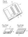
- In recent years, a card-type memory device, such as an IC card, has been put into practical use. Some IC cards comprise a detachable card-type module which contains a memory. Fig. 4 shows an example of the card-type module commonly used in portable computers. Figs. 5(a), 5(b) and 6 show a semiconductor module used for the card-type module. In particular, Fig. 5(a) is a perspective view of a surface of the semiconductor module which is sealed by resin. Fig. 5(b) is a perspective view of the bottom surface of the semiconductor module on which terminals connected to the external circuit are provided. Fig. 6 is a cross-sectional view of the semiconductor module. In the semiconductor module shown in Fig. 6, a
semiconductor chip 25 is bonded on the surface of asubstrate 13, and abonding pad 29 of thesemiconductor chip 25 is connected by agold wire 27 to a terminal formed on thesubstrate 13 to be connected to the semiconductor chip. The semiconductor chip may be connected to the chip connecting terminal on the substrate by a flip-chip bonding technique using a bump. Thesemiconductor chip 25 is then sealed by amolding portion 14. Typically, a non-volatile semiconductor memory, such as a flash EEPROM, is used as thesemiconductor chip 25. The periphery of thesubstrate 13 is exposed to the outside and surrounds theresin mold section 14. The opposite surface of the substrate is provided with aplain connection terminal 12 which can be connected to external circuits. Commonly, theexternal connection terminal 12 is connected to thechip connecting terminal 26 by a throughhole 28. - Referring to Fig. 4, a
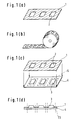
semiconductor module 10 formed in the above-mentioned manner is bonded to a concave portion 11a of amodule supporter 11 made of resin or plastic, so that thesemiconductor module 10 is embedded in the concave portion 11a. Theexternal connection terminals 12 are exposed to the outer environment on substantially the same plain as that of themodule supporter 11. The periphery portion of thesubstrate 13 is bonded to the concave portion 11a of themodule supporter 11, preferably, with the use of liquid or sheet-like adhesive. - Figs. 7(a)-7(c) show one method of bonding a semiconductor module and a module supporter with the sheet-like adhesive piece. As shown in Fig. 7 (a), a
semiconductor module 17 is cut away from asubstrate 15 which has a plurality of serially arranged semiconductor modules. In particular, aresin mold section 16 corresponding to eachsemiconductor module 17 is serially arranged on thesubstrate 15. Next,adhesive pieces 19, each having a shape corresponding to a bonding interface of a semiconductor module and a module supporter, are cut away from anadhesive sheet 18, as shown in Fig. 7(b). Each adhesive piece has a shape of a frame. Theadhesive sheet 18 and theadhesive pieces 19 have adhesive materials on both sides. Eachadhesive piece 19 is then applied to the concave portion 11a of themodule supporter 11, as shown in Fig. 7(c). Finally, as shown in Fig. 7(c), thesemiconductor module 17 is placed substantially on top of theadhesive piece 19 for bonding to themodule supporter 11. - Fig. 8 shows an alternative method for bonding a semiconductor module and a module supporter with the sheet-like adhesive pieces. As shown in Fig. 8(a), a
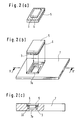
semiconductor module 17 is cut away from asubstrate 15 which has a plurality of serially arranged semiconductor modules. Next,adhesive pieces 19 each having the same area as that of one semiconductor module are cut away from anadhesive sheet 18, as shown in Fig. 8(b). Subsequently, each of theadhesive pieces 19 is applied to thesemiconductor module 17, as shown in Fig. 8(c). Thesemiconductor module 17 is then placed substantially on top of the concave portion 11a of themodule supporter 11, such that thesemiconductor module 17 applied with theadhesive pieces 19 is bonded to the concave portion 11a of themodule supporter 11, as shown in Fig. 8(d). - Alternatively, when a liquid adhesive is used to bond the
semiconductor module 17 with themodule supporter 11, asemiconductor module 17 is cut away from a plurality of semiconductor modules formed on asubstrate 15. Then, the liquid adhesive is applied to the portion of the module supporter, on which the semiconductor module is to be bonded. - In the conventional process described above, it is difficult to cut away from the adhesive sheet the adhesive pieces each having the shape of the bonding portion of the
module supporter 11 for bonding the semiconductor module and the module supporter. To cut the adhesive pieces having the corresponding shape of the bonding portion with a die, the adhesive sheet must be divided into three portions (i.e., outer portion, frame portion, and inner portion), and thus a special die is required. Further, the cutting edge of the die become dull after continuous use so that the adhesive material from the adhesive sheet smears over the die. - In addition, the adhesive piece cut in the shape of the bonding portion of the
module supporter 11 is very thin, small, sticky and light. As a result, handling of the adhesive piece can be problematic. In particular, if the user wishes to perform the bonding process automatically, it may be impossible for a machine to deal with such an adhesive piece with ease. - It is also difficult to precisely align the adhesive pieces with the bonding portion of the
module supporter 11. In particular, if the adhesive piece is misaligned, the adhesive piece may undesirably protrude beyond the bonding surface and encroach on the external connection terminals. This misalignment results in a undesirable appearance and increases the defect rate in the final products. - To prevent such misalignment of the adhesive piece to the bonding surface, an adhesive piece having a smaller adhesive area than that of the bonding portion might be used. However, a small adhesive piece does not have strong adhesion.
- It is an object of the present invention to provide a method for packaging a semiconductor module with a module supporter using an adhesive piece without the above described problems.
- According to one embodiment of the present invention, a semiconductor substrate has a plurality of semiconductor modules, where each semiconductor module has a semiconductor chip covered with a protective material, such as resin, on a first surface and a connector formed on a second surface which is electrically connected to the semiconductor chip. An adhesive layer is applied to the first surface of the substrate. The adhesive layer has a plurality of opening portions arranged to correspond to the plurality of semiconductor modules on the substrate. The adhesive layer may be wound onto a reel for easy handling. Then the substrate and the adhesive layer are cut into individual substrates, each having the semiconductor chip so that each semiconductor module has the adhesive layer on a periphery of the protective material. An individual substrate containing a semiconductor module is then bonded to a supporter having a concave portion for holding the semiconductor module.
- In the above embodiment, it is preferable that the protective material covering the semiconductor chip be smaller than the concave portion of the supporter so that any bending pressure applied to the supporter is not substantially transferred to the semiconductor chip residing inside the protective material.
- According to another embodiment of the present invention, the adhesive layer may have a plurality of adhesive portions each shaped like a frame to surround the periphery of the semiconductor module. The plurality of adhesive portions are arranged to correspond to the plurality of semiconductor modules on the substrate.
- These and other aspects, features and advantages of the present invention will be better understood by studying the detailed description in conjunction with the drawings and the accompanying claims.
- A detailed description of embodiments of the present invention will be made with reference to the accompanying drawings, wherein like numerals designate corresponding parts in the several figures.
- Figs. 1(a)-1(d) show a first embodiment of the present invention where an adhesive layer is being applied to a substrate;
- Figs. 2(a)-2(c) show a first embodiment of the present invention where a semiconductor module is bonded to a support module;
- Figs. 3(a)-3(c) show a second embodiment of the present invention;
- Fig. 4 shows a card-type module;
- Figs. 5(a) and 5(b) show a semiconductor module;
- Fig. 6 is a sectional view of the semiconductor module;
- Figs. 7(a)-7(c) show a conventional bonding method; and
- Figs. 8 (a)-8(d) show another conventional bonding method.
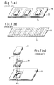
- Preferred embodiments of the present invention are described in detail hereinbelow with reference to the attached drawings. Figs. 1(a)-1(d) and 2(a)-2(c) show a first embodiment of the present invention. In particular, Fig. 1(c) shows a plurality of semiconductor chips (residing inside the molding portions 3) arranged at a predetermined interval on a substrate 4 formed of any suitable material, such as resin. The adhesive sheet 1 having double adhesive sides is formed by applying adhesive on one side of peelable paper (not shown) releasably secured to the adhesive sheet and has opening
portions 2, as shown in Fig. 1(a). The openingportions 2 are formed to correspond to the arrangement of themolding portion 3 of the semiconductor modules. - The adhesive sheet 1 with a peelable paper may be wound into a reel as shown in Fig. 1(b). As shown in Fig. 1(c), the opening
portions 2 of the adhesive sheet 1 are aligned with themolding portions 3 and applied to the substrate 4 on which a plurality of thesemiconductor modules 5 are arranged. - Next, as shown in Fig. 1(d), the substrate 4 on which the adhesive sheet 1 is applied is cut along the die lines 23. In the preferred embodiment, the adhesive sheet 1 and the
semiconductor modules 5 are simultaneously cut to result in individual modules, one of which is shown in Fig. 2(a). Thesemiconductor modules 5 each have a properly alignedadhesive piece 6 around themolding portions 3. The peelable paper may be detached from the adhesive piece either before or after the die-cutting process. Finally, as shown in Fig. 2(b), thesemiconductor module 5 with theadhesive piece 6 is bonded to a concave portion 7a of themodule supporter 7. - As an alternative to bonding the adhesive sheet 1 and the
adhesive piece 6 to the substrate 4, thermal compression may be used. Thermal compression may be used when the adhesive sheet 1 is applied to the substrate 4 having a plurality of the semiconductor modules, or when thesemiconductor modules 5 are bonded to themodule supporter 7. - When the adhesive sheet 1 is applied to the substrate 4 by thermal compression, the adhesive sheet 1 may be temporarily attached to the substrate 4 until the
semiconductor module 5 is bonded to themodule supporter 7 by thermal compression. If the adhesive sheet 1 uses an adhesive not requiring the thermal compression step, the above-mentioned step need not be performed. - When the adhesive sheet 1 is applied to the substrate 4 having a plurality of the semiconductor modules, the adhesive sheet 1 may be applied simultaneously on the entire surface of the substrate 4. Alternatively, the adhesive sheet 1 may be sequentially applied to each
module portion 3. - As described above, in the preferred embodiment, an adhesive sheet 1 having a plurality of holes is used to simultaneously bond against a plurality of semiconductor sheets. By performing the simultaneous bonding process in such a manner, the opening
portions 2 and themolding portions 3 are properly aligned and may require only one bonding process. - Fig. 2(c) shows a cross-sectional view of the devices shown in Fig. 2(b) taken along a line X-X . As shown in Fig. 2(c), the
semiconductor module 5 applied with theadhesive piece 6 on its periphery is bonded to the concave portion 7a of themodule supporter 7. As a result, the bending stress exerted on themodule supporter 7 is not forced upon asemiconductor chip 25 contained in themolding portion 3, because the size of themolding 3 is smaller than that of the concave portion 7a. In other words, agap 33 created between themolding portion 3 and the bottom of the concave portion 7a substantially blocks any pressure applied to themolding portion 3. - To alleviate the application pressure, the adhesive sheet 1 is not applied on top the
molding portion 3. If the adhesive sheet 1 is applied to the entire surface of thesemiconductor module 5 so as to cover the substantiallyentire molding portion 3, the bending stress or pressure exerted on themodule supporter 7 may be transferred to thesemiconductor chip 25 thus damaging the same. In any event, the adhesive sheet 1 cannot easily be applied evenly to thesemiconductor module 5 due to the irregular and non-flat surface of themolding portion 3. - Figs. 3(a)-3(c) shows a second embodiment of the present invention. In particular, Fig. 3(c) shows a plurality of semiconductor chips (residing inside the molding portions 3) arranged at a predetermined interval on a substrate 4 formed of material such as resin or tape. As shown in Fig. 3(a), the
adhesive sheet 22 is formed, for example, by applying anadhesive piece 8 formed in a shape of a frame or a rectangle on the surface of peelable paper. Theadhesive piece 8 is formed in a shape having an inner dimensions substantially the same as that of the bonding interface of the semiconductor module and the module supporter and an outer dimensions larger than the bonding interface. Theadhesive piece 8 is positioned on the peelable paper to correspond the arrangement of themolding portions 3 on the substrate 4. Theadhesive sheet 22 has opening portions 9a which are formed by die-cutting the peelable paper on the portions corresponding to the inner dimensions of the frame-shapedadhesive piece 8. Similar to the first embodiment of the present invention, theadhesive sheet 22 may be wound onto a reel as shown in Fig. 3(b). - Then, as shown in Fig. 3(c), the
adhesive pieces 8 on theadhesive sheet 9 are sequentially applied to the substrate 4 having a plurality of thesemiconductor modules 5, such that themolding portion 3 is inserted in the opening portions 9a. Next, the substrate 4 having theadhesive pieces 8 is cut along the die lines 24. As a result, theadhesive pieces 8 and the semiconductor modules are simultaneously cut. Consequently, thesemiconductor modules 5 having theadhesive piece 6 shown in Fig. 2(a) are rendered. Thepeelable paper 9 may be detached from theadhesive piece 6 either before or after the die-cutting process. Finally, as shown in Fig. 2(b), thesemiconductor module 5 with theadhesive piece 6 is bonded to a concave portion 7a of themodule supporter 7. - As described above, the second embodiment is intended to simultaneously bond an adhesive sheet to a plurality of semiconductor sheets. By performing the simultaneous bonding process in such a manner, the opening
portions 2 and themolding portions 3 can be properly aligned and may require only one bonding process. - As described above, according to the various embodiments of the present invention, an adhesive sheet having a plurality of holes is simultaneously bond to a plurality of semiconductor sheets. Thus, the process period can be shortened and the alignment can be performed with more ease.
- In addition, according to the present invention, the semiconductor modules and the adhesive pieces are simultaneously die-cut, and the number of steps in manufacturing process is reduced. Further, the semiconductor modules are die-cut after the adhesive piece is applied, and thus the adhesion of the adhesive piece to the external connection electrodes, which is caused by the misalignment of the adhesive piece can be prevented. By virtue of this feature, the defect rate is reduced.
- Additionally, according to the present invention, the entire bonding portion of the semiconductor module can be applied with the adhesive. Accordingly, adhesive strength is increased, and the mechanical strength of an IC card using the semiconductor device formed in such a manner is improved, thus improving reliability of the device.
- Since the
molding portion 3 has a smaller size than that of the concave portion 7a of the module supporter, and the top surface of themolding portion 3 is not in contact with the module supporter, the bending stress exerted on the module supporter is not transferred to the semiconductor chip residing in themolding portion 3. - The above-mentioned process according to the present invention may be used with semiconductor modules having
external connection terminals 12 on the opposite surface of the molding surface, as shown in Fig. 5(b). The semiconductor module constructed using the present invention is preferably mounted in amodule supporter 11 formed of resin having, for example, a length, a width, and a thickness of 37 mm x 45 mm x 0.76 mm, respectively. - The card-type module is connected to an adapter card (not shown). The adapter card may be configured to be used with a PCMCIA card slot or the like. The adapter card includes an insertion hole for receiving a card-type module therein, and a standard connector for attaching to, for example, a PCMCIA card slot of a personal computer. The adapter card has an interior provided with a connector for being contacted with the external-connection terminal of the card-type module and an interface circuit for functioning as an interface between the card-type module and an external apparatus, such as a personal computer. Also, the adapter card may be of types other than a PCMCIA card. Furthermore, a connector may be provided, together with the interface circuit, in the main body of a personal computer or a camera to communicate with the external-connection terminal of the card-type module.
- While the description above refers to particular embodiments of the present invention, it will be understood that many modifications may be made without departing from the spirit thereof. The accompanying claims are intended to cover such modifications as would fall within the true scope and spirit of the present invention. The presently disclosed embodiments are therefore to be considered in all respects as illustrative and not restrictive, the scope of the invention being indicated by the appended claims, rather than the foregoing description, and all changes which come within the meaning and range of equivalency of the claims are therefore intended to be embraced therein.
Claims (13)
- A method of manufacturing a semiconductor device mountable in a supporter, the method comprising:preparing a plurality of semiconductor modules, all the semiconductor modules being on one substrate, in which each semiconductor module has a semiconductor chip covered with a protective material on a first surface of the substrate and a connector formed on a second surface of the substrate and electrically connected to the semiconductor chip;applying an adhesive layer to the first surface of the substrate, the adhesive layer having a plurality of opening portions arranged to positionally correspond to the plurality of semiconductor modules on the substrate;cutting both the substrate and the adhesive layer into individual substrates having the semiconductor chip so that each semiconductor module has the adhesive layer on a periphery of the protective material; andbonding each one of the individual substrates containing a semiconductor module to a corresponding supporter.
- A method according to claim 1, wherein the adhesive layer is wound onto a reel.
- A method according to claim 1, wherein the protective material is resin.
- A method according to claim 1, wherein the supporter has a concave portion for holding the semiconductor module, in which the periphery of the protective material is securely attached to the concave portion so that the connector to the semiconductor chip is accessible.
- A method according to claim 4, wherein the protective material covering the semiconductor chip is smaller than the concave portion of the supporter so that a gap is formed between the protective material and the supporter.
- A method according to claim 1, wherein the adhesive layer removably secured to a peelable layer.
- A method of manufacturing a semiconductor device mountable in a supporter, the method comprising:preparing a plurality of semiconductor modules, all the semiconductor modules being on one substrate, in which each semiconductor module has a semiconductor chip covered with a protective material on a first surface of the substrate and a connector formed on a second surface of the substrate and electrically connected to the semiconductor chip;applying an adhesive layer to the first surface of the substrate, the adhesive layer having a plurality of adhesive portions each shaped to surround the periphery of the semiconductor module, wherein the plurality of adhesive portions are arranged to positionally correspond to the plurality of semiconductor modules on the substrate;cutting both the substrate and the adhesive layer into individual substrates having the semiconductor chip so that each semiconductor module has the adhesive layer on a periphery of the protective; andboncling each one of the individual substrates containing a semiconductor module to a corresponding supporter.
- A method according to claim 7, wherein the adhesive layer is wound onto a reel.
- A method according to claim 7, wherein the adhesive layer is resin.
- A method according to claim 7, wherein the supporter has a concave portion for hodding the semiconductor nodule, in which the periphery of the protective material is securely attached to the concave portion so that the connector to the semiconductor chip is accessible.
- A method according to claim 10, wherein the protective material covering the semiconductor chip is smaller than the concave portion of the supporter so that a gap is formed between the protective material and the supporter.
- A method according to claim 7, wherein the adhesive layer includes the plurality of adhesive portions removably attached to a peelable paper layer.
- A method according to claim 7, wherein each adhesive portion has a rectangular frame shape to match a rectangular shape of the protective material covering the semiconductor chip.
Applications Claiming Priority (3)
| Application Number | Priority Date | Filing Date | Title |
|---|---|---|---|
| JP10535996 | 1996-04-25 | ||
| JP10535996 | 1996-04-25 | ||
| JP105359/96 | 1996-04-25 |
Publications (3)
| Publication Number | Publication Date |
|---|---|
| EP0803901A2 true EP0803901A2 (en) | 1997-10-29 |
| EP0803901A3 EP0803901A3 (en) | 1999-09-22 |
| EP0803901B1 EP0803901B1 (en) | 2006-08-16 |
Family
ID=14405537
Family Applications (1)
| Application Number | Title | Priority Date | Filing Date |
|---|---|---|---|
| EP97106644A Expired - Lifetime EP0803901B1 (en) | 1996-04-25 | 1997-04-22 | Method of mounting a plurality of semiconductor devices in corresponding supporters |
Country Status (6)
| Country | Link |
|---|---|
| US (1) | US5956601A (en) |
| EP (1) | EP0803901B1 (en) |
| KR (1) | KR100269850B1 (en) |
| CN (1) | CN1092399C (en) |
| DE (1) | DE69736499T2 (en) |
| TW (1) | TW334619B (en) |
Cited By (1)
| Publication number | Priority date | Publication date | Assignee | Title |
|---|---|---|---|---|
| WO2001095486A1 (en) * | 2000-06-06 | 2001-12-13 | Sawtek Inc. | System and method for array processing of surface acoustic wave devices |
Families Citing this family (14)
| Publication number | Priority date | Publication date | Assignee | Title |
|---|---|---|---|---|
| FR2773900B1 (en) * | 1998-01-22 | 2000-02-18 | Gemplus Card Int | CARD WITH INTEGRATED CONTACT CIRCUIT (S), COMPRISING A DETACHABLE MINICARD |
| SG80077A1 (en) * | 1998-10-19 | 2001-04-17 | Sony Corp | Semiconductor integrated circuit card manufacturing method, and semiconductor integrated circuit card |
| JP2002092575A (en) * | 2000-09-19 | 2002-03-29 | Mitsubishi Electric Corp | Small card and manufacturing method thereof |
| JP4162930B2 (en) * | 2002-06-25 | 2008-10-08 | 富士機械製造株式会社 | Substrate transfer device for electronic component mounting equipment |
| JP4002143B2 (en) * | 2002-07-10 | 2007-10-31 | 株式会社ルネサステクノロジ | Manufacturing method of semiconductor device |
| CN100336072C (en) * | 2004-06-16 | 2007-09-05 | 台湾典范半导体股份有限公司 | Memory card constituting method and structure thereof |
| USD794641S1 (en) * | 2009-01-07 | 2017-08-15 | Samsung Electronics Co., Ltd. | Memory device |
| USD794034S1 (en) * | 2009-01-07 | 2017-08-08 | Samsung Electronics Co., Ltd. | Memory device |
| USD794643S1 (en) * | 2009-01-07 | 2017-08-15 | Samsung Electronics Co., Ltd. | Memory device |
| USD795261S1 (en) * | 2009-01-07 | 2017-08-22 | Samsung Electronics Co., Ltd. | Memory device |
| USD795262S1 (en) * | 2009-01-07 | 2017-08-22 | Samsung Electronics Co., Ltd. | Memory device |
| USD794644S1 (en) * | 2009-01-07 | 2017-08-15 | Samsung Electronics Co., Ltd. | Memory device |
| USD794642S1 (en) * | 2009-01-07 | 2017-08-15 | Samsung Electronics Co., Ltd. | Memory device |
| CN111640677B (en) * | 2020-03-02 | 2022-04-26 | 浙江集迈科微电子有限公司 | Method for placing chips in groove |
Citations (2)
| Publication number | Priority date | Publication date | Assignee | Title |
|---|---|---|---|---|
| US4701236A (en) * | 1985-04-12 | 1987-10-20 | U.S. Philips Corporation | Method of manufacturing an electronic identification card |
| EP0426406A2 (en) * | 1989-10-31 | 1991-05-08 | Citizen Watch Co., Ltd. | IC card having an integrated circuit module |
Family Cites Families (34)
| Publication number | Priority date | Publication date | Assignee | Title |
|---|---|---|---|---|
| FR2439478A1 (en) * | 1978-10-19 | 1980-05-16 | Cii Honeywell Bull | FLAT HOUSING FOR DEVICES WITH INTEGRATED CIRCUITS |
| JPS5623759A (en) * | 1979-08-01 | 1981-03-06 | Hitachi Ltd | Resin-sealed semiconductor device and manufacture thereof |
| JP2582013B2 (en) * | 1991-02-08 | 1997-02-19 | 株式会社東芝 | Resin-sealed semiconductor device and method of manufacturing the same |
| IT1212711B (en) * | 1983-03-09 | 1989-11-30 | Ates Componenti Elettron | SEMI-CONDUCTOR AFORMA FLAT BOARD DEVICE WITH ELECTRIC CONTACTS ON BOTH SIDES AND PROCEDURE FOR ITS MANUFACTURE. |
| DE3546780C2 (en) * | 1985-09-02 | 1996-04-25 | Amphenol Corp | Contact unit for chip card access |
| JPS6478397A (en) * | 1987-09-18 | 1989-03-23 | Mitsubishi Electric Corp | Ic card writing system |
| FR2624635B1 (en) * | 1987-12-14 | 1991-05-10 | Sgs Thomson Microelectronics | ELECTRONIC COMPONENT HOLDER FOR MEMORY CARD AND PRODUCT THUS OBTAINED |
| JP2510694B2 (en) * | 1988-09-16 | 1996-06-26 | 大日本印刷株式会社 | IC card |
| US5068714A (en) * | 1989-04-05 | 1991-11-26 | Robert Bosch Gmbh | Method of electrically and mechanically connecting a semiconductor to a substrate using an electrically conductive tacky adhesive and the device so made |
| DE69033262T2 (en) * | 1989-04-13 | 2000-02-24 | Sandisk Corp | EEPROM card with replacement of faulty memory cells and buffer |
| US5535328A (en) * | 1989-04-13 | 1996-07-09 | Sandisk Corporation | Non-volatile memory system card with flash erasable sectors of EEprom cells including a mechanism for substituting defective cells |
| JPH02301155A (en) * | 1989-05-16 | 1990-12-13 | Citizen Watch Co Ltd | Method of fixing ic module |
| FR2659157B2 (en) * | 1989-05-26 | 1994-09-30 | Lemaire Gerard | METHOD FOR MANUFACTURING A CARD, SAID CARD, AND CARD OBTAINED BY THIS PROCESS. |
| US5200362A (en) * | 1989-09-06 | 1993-04-06 | Motorola, Inc. | Method of attaching conductive traces to an encapsulated semiconductor die using a removable transfer film |
| US5153818A (en) * | 1990-04-20 | 1992-10-06 | Rohm Co., Ltd. | Ic memory card with an anisotropic conductive rubber interconnector |
| JP2874279B2 (en) * | 1990-05-10 | 1999-03-24 | 三菱電機株式会社 | Method for manufacturing thin semiconductor device |
| JPH0416396A (en) * | 1990-05-10 | 1992-01-21 | Mitsubishi Electric Corp | Semiconductor device card |
| JP2560895B2 (en) * | 1990-07-25 | 1996-12-04 | 三菱電機株式会社 | IC card manufacturing method and IC card |
| FR2673017A1 (en) * | 1991-02-18 | 1992-08-21 | Schlumberger Ind Sa | METHOD FOR MANUFACTURING AN ELECTRONIC MODULE FOR A MEMORY CARD AND ELECTRONIC MODULE THUS OBTAINED. |
| US5663901A (en) * | 1991-04-11 | 1997-09-02 | Sandisk Corporation | Computer memory cards using flash EEPROM integrated circuit chips and memory-controller systems |
| US5284784A (en) * | 1991-10-02 | 1994-02-08 | National Semiconductor Corporation | Buried bit-line source-side injection flash memory cell |
| US5299089A (en) * | 1991-10-28 | 1994-03-29 | E. I. Dupont De Nemours & Co. | Connector device having two storage decks and three contact arrays for one hard disk drive package or two memory cards |
| FR2686172B1 (en) * | 1992-01-14 | 1996-09-06 | Gemplus Card Int | PLUG - IN CARD FOR A MICROCOMPUTER FORMING A CARD READER WITH FLUSHED CONTACTS. |
| US5169056A (en) * | 1992-02-21 | 1992-12-08 | Eastman Kodak Company | Connecting of semiconductor chips to circuit substrates |
| US5247423A (en) * | 1992-05-26 | 1993-09-21 | Motorola, Inc. | Stacking three dimensional leadless multi-chip module and method for making the same |
| JP2674924B2 (en) * | 1992-07-13 | 1997-11-12 | 積水化学工業株式会社 | IC card manufacturing apparatus and method of manufacturing adhesive piece supply roll used for the same |
| US5469399A (en) * | 1993-03-16 | 1995-11-21 | Kabushiki Kaisha Toshiba | Semiconductor memory, memory card, and method of driving power supply for EEPROM |
| JPH0737049A (en) * | 1993-07-23 | 1995-02-07 | Toshiba Corp | External storage |
| TW272311B (en) * | 1994-01-12 | 1996-03-11 | At & T Corp | |
| US5480842A (en) * | 1994-04-11 | 1996-01-02 | At&T Corp. | Method for fabricating thin, strong, and flexible die for smart cards |
| KR0144818B1 (en) * | 1994-07-25 | 1998-08-17 | 김광호 | Nand type flash memory ic card |
| US5508971A (en) * | 1994-10-17 | 1996-04-16 | Sandisk Corporation | Programmable power generation circuit for flash EEPROM memory systems |
| KR0152042B1 (en) * | 1995-04-15 | 1998-10-15 | 김광호 | Nand type flash memory i.c. card recording apparatus |
| US5596532A (en) * | 1995-10-18 | 1997-01-21 | Sandisk Corporation | Flash EEPROM self-adaptive voltage generation circuit operative within a continuous voltage source range |
-
1997
- 1997-04-17 US US08/839,358 patent/US5956601A/en not_active Expired - Lifetime
- 1997-04-21 TW TW086105149A patent/TW334619B/en not_active IP Right Cessation
- 1997-04-22 DE DE69736499T patent/DE69736499T2/en not_active Expired - Lifetime
- 1997-04-22 EP EP97106644A patent/EP0803901B1/en not_active Expired - Lifetime
- 1997-04-23 KR KR1019970015183A patent/KR100269850B1/en not_active IP Right Cessation
- 1997-04-24 CN CN97110389A patent/CN1092399C/en not_active Expired - Fee Related
Patent Citations (2)
| Publication number | Priority date | Publication date | Assignee | Title |
|---|---|---|---|---|
| US4701236A (en) * | 1985-04-12 | 1987-10-20 | U.S. Philips Corporation | Method of manufacturing an electronic identification card |
| EP0426406A2 (en) * | 1989-10-31 | 1991-05-08 | Citizen Watch Co., Ltd. | IC card having an integrated circuit module |
Non-Patent Citations (2)
| Title |
|---|
| PATENT ABSTRACTS OF JAPAN vol. 014, no. 271 (M-0983), 12 June 1990 (1990-06-12) & JP 02 080299 A (DAINIPPON PRINTING CO LTD), 20 March 1990 (1990-03-20) * |
| PATENT ABSTRACTS OF JAPAN vol. 018, no. 231 (M-1599), 27 April 1994 (1994-04-27) & JP 06 024187 A (SEKISUI CHEM CO LTD), 1 February 1994 (1994-02-01) * |
Cited By (2)
| Publication number | Priority date | Publication date | Assignee | Title |
|---|---|---|---|---|
| WO2001095486A1 (en) * | 2000-06-06 | 2001-12-13 | Sawtek Inc. | System and method for array processing of surface acoustic wave devices |
| US6928718B2 (en) | 2000-06-06 | 2005-08-16 | Sawtekk, Inc. | Method for array processing of surface acoustic wave devices |
Also Published As
| Publication number | Publication date |
|---|---|
| CN1173041A (en) | 1998-02-11 |
| DE69736499T2 (en) | 2007-08-16 |
| US5956601A (en) | 1999-09-21 |
| EP0803901A3 (en) | 1999-09-22 |
| DE69736499D1 (en) | 2006-09-28 |
| TW334619B (en) | 1998-06-21 |
| KR100269850B1 (en) | 2000-10-16 |
| CN1092399C (en) | 2002-10-09 |
| EP0803901B1 (en) | 2006-08-16 |
Similar Documents
| Publication | Publication Date | Title |
|---|---|---|
| EP0803901B1 (en) | Method of mounting a plurality of semiconductor devices in corresponding supporters | |
| US7094633B2 (en) | Method for efficiently producing removable peripheral cards | |
| US5600175A (en) | Apparatus and method for flat circuit assembly | |
| US6462273B1 (en) | Semiconductor card and method of fabrication | |
| US4549247A (en) | Carrier element for IC-modules | |
| JP2849594B2 (en) | Electronic module sealing method | |
| EP1639644B1 (en) | Integrated circuit package having stacked integrated circuits and method therefor | |
| KR100280170B1 (en) | Substrate for semiconductor device and manufacturing method thereof, semiconductor device, card type module and information storage device | |
| US5184207A (en) | Semiconductor die packages having lead support frame | |
| EP0435093A2 (en) | Thin, molded, surface mount electronic device | |
| US20030029920A1 (en) | Molded memory module and method of making the module absent a substrate support | |
| US6025997A (en) | Chip module for semiconductor chips having arbitrary footprints | |
| US20010001507A1 (en) | Substrate for a semiconductor device, a semiconductor device, a card type module, and a data memory device | |
| KR100572425B1 (en) | Pc adapter cards and method of manufacturing the same | |
| US20040043551A1 (en) | Method of making a microelectronic assembly | |
| JP3485736B2 (en) | Semiconductor device and manufacturing method thereof | |
| JPH02177553A (en) | Integrated circuit device and manufacture thereof | |
| JP3976984B2 (en) | Semiconductor device and manufacturing method thereof | |
| JPH1056028A (en) | Manufacturing method of semiconductor device | |
| JP2007034786A (en) | Composite ic card and its manufacturing method | |
| JPS63317395A (en) | Ic card | |
| JPS60129897A (en) | Miniature electronic device | |
| JPH0276798A (en) | Manufacture of integrated circuit device | |
| JP2010251764A (en) | Sealing method for enhancing adhesive strength between package material and substrate | |
| JPS6359593A (en) | Mounting method in portable medium |
Legal Events
| Date | Code | Title | Description |
|---|---|---|---|
| PUAI | Public reference made under article 153(3) epc to a published international application that has entered the european phase |
Free format text: ORIGINAL CODE: 0009012 |
|
| 17P | Request for examination filed |
Effective date: 19970422 |
|
| AK | Designated contracting states |
Kind code of ref document: A2 Designated state(s): DE FR GB |
|
| PUAL | Search report despatched |
Free format text: ORIGINAL CODE: 0009013 |
|
| AK | Designated contracting states |
Kind code of ref document: A3 Designated state(s): DE FR GB |
|
| GRAP | Despatch of communication of intention to grant a patent |
Free format text: ORIGINAL CODE: EPIDOSNIGR1 |
|
| GRAS | Grant fee paid |
Free format text: ORIGINAL CODE: EPIDOSNIGR3 |
|
| GRAA | (expected) grant |
Free format text: ORIGINAL CODE: 0009210 |
|
| AK | Designated contracting states |
Kind code of ref document: B1 Designated state(s): DE FR GB |
|
| REG | Reference to a national code |
Ref country code: GB Ref legal event code: FG4D |
|
| REF | Corresponds to: |
Ref document number: 69736499 Country of ref document: DE Date of ref document: 20060928 Kind code of ref document: P |
|
| ET | Fr: translation filed | ||
| PLBE | No opposition filed within time limit |
Free format text: ORIGINAL CODE: 0009261 |
|
| STAA | Information on the status of an ep patent application or granted ep patent |
Free format text: STATUS: NO OPPOSITION FILED WITHIN TIME LIMIT |
|
| 26N | No opposition filed |
Effective date: 20070518 |
|
| PGFP | Annual fee paid to national office [announced via postgrant information from national office to epo] |
Ref country code: DE Payment date: 20120425 Year of fee payment: 16 |
|
| PGFP | Annual fee paid to national office [announced via postgrant information from national office to epo] |
Ref country code: FR Payment date: 20120504 Year of fee payment: 16 Ref country code: GB Payment date: 20120418 Year of fee payment: 16 |
|
| GBPC | Gb: european patent ceased through non-payment of renewal fee |
Effective date: 20130422 |
|
| PG25 | Lapsed in a contracting state [announced via postgrant information from national office to epo] |
Ref country code: GB Free format text: LAPSE BECAUSE OF NON-PAYMENT OF DUE FEES Effective date: 20130422 Ref country code: DE Free format text: LAPSE BECAUSE OF NON-PAYMENT OF DUE FEES Effective date: 20131101 |
|
| REG | Reference to a national code |
Ref country code: FR Ref legal event code: ST Effective date: 20131231 |
|
| REG | Reference to a national code |
Ref country code: DE Ref legal event code: R119 Ref document number: 69736499 Country of ref document: DE Effective date: 20131101 |
|
| PG25 | Lapsed in a contracting state [announced via postgrant information from national office to epo] |
Ref country code: FR Free format text: LAPSE BECAUSE OF NON-PAYMENT OF DUE FEES Effective date: 20130430 |