EP0803856A1 - Display - Google Patents
Display Download PDFInfo
- Publication number
- EP0803856A1 EP0803856A1 EP96933645A EP96933645A EP0803856A1 EP 0803856 A1 EP0803856 A1 EP 0803856A1 EP 96933645 A EP96933645 A EP 96933645A EP 96933645 A EP96933645 A EP 96933645A EP 0803856 A1 EP0803856 A1 EP 0803856A1
- Authority
- EP
- European Patent Office
- Prior art keywords
- clock signal
- signal
- circuit
- duty ratio
- phase
- Prior art date
- Legal status (The legal status is an assumption and is not a legal conclusion. Google has not performed a legal analysis and makes no representation as to the accuracy of the status listed.)
- Withdrawn
Links
Images


Classifications
-
- G—PHYSICS
- G09—EDUCATION; CRYPTOGRAPHY; DISPLAY; ADVERTISING; SEALS
- G09G—ARRANGEMENTS OR CIRCUITS FOR CONTROL OF INDICATING DEVICES USING STATIC MEANS TO PRESENT VARIABLE INFORMATION
- G09G3/00—Control arrangements or circuits, of interest only in connection with visual indicators other than cathode-ray tubes
- G09G3/20—Control arrangements or circuits, of interest only in connection with visual indicators other than cathode-ray tubes for presentation of an assembly of a number of characters, e.g. a page, by composing the assembly by combination of individual elements arranged in a matrix no fixed position being assigned to or needed to be assigned to the individual characters or partial characters
- G09G3/34—Control arrangements or circuits, of interest only in connection with visual indicators other than cathode-ray tubes for presentation of an assembly of a number of characters, e.g. a page, by composing the assembly by combination of individual elements arranged in a matrix no fixed position being assigned to or needed to be assigned to the individual characters or partial characters by control of light from an independent source
- G09G3/36—Control arrangements or circuits, of interest only in connection with visual indicators other than cathode-ray tubes for presentation of an assembly of a number of characters, e.g. a page, by composing the assembly by combination of individual elements arranged in a matrix no fixed position being assigned to or needed to be assigned to the individual characters or partial characters by control of light from an independent source using liquid crystals
- G09G3/3611—Control of matrices with row and column drivers
-
- G—PHYSICS
- G09—EDUCATION; CRYPTOGRAPHY; DISPLAY; ADVERTISING; SEALS
- G09G—ARRANGEMENTS OR CIRCUITS FOR CONTROL OF INDICATING DEVICES USING STATIC MEANS TO PRESENT VARIABLE INFORMATION
- G09G5/00—Control arrangements or circuits for visual indicators common to cathode-ray tube indicators and other visual indicators
- G09G5/18—Timing circuits for raster scan displays
Definitions
- the present invention relates generally to display devices with an optical modulation layer such as a liquid crystal layer, and more particularly to liquid crystal display (LCD) devices.
- an optical modulation layer such as a liquid crystal layer
- LCD liquid crystal display
- Fig. 13 is a diagram showing a configuration of driver circuit of an active-matrix LCD device.
- Numeral 102 designates an LCD panel which is constituted from a first electrode substrate having a plurality of pixel electrodes as arranged in a matrix form, for example, a second electrode substrate with an opposed electrode opposing the pixel electrodes, and a liquid crystal provided as an optical modulation layer disposed between these first and second electrode substrates through orientation films.
- Numeral 104 designates a predetermined number of signal-line driver circuits each of which output an image signal, to the signal lines connected to the pixel electrodes, via switching elements such as a thin-film transistor (referred to as "TFT" hereinafter), of the LCD panel 102.
- TFT thin-film transistor
- Numeral 108 indicates a scanning-line driver circuit which serves to output a scanning signal to the scanning lines for control of switching element being electrically connected to the pixel electrodes of LCD panel 102.
- Numeral 110 is a control circuit which generates and supplies several signals, including image data Data, a horizontal clock signal CK1 and a start signal ST, to the signal-line driver circuits 104, and which generates and supplies several signals including a vertical clock signal CK2 to the scanning-line driver circuit 108.
- the control circuit 110 comprises a horizontal clock signal generator circuit section 109, a signal generator circuit section 112, and a delay time adjuster circuit section 113.
- the horizontal clock signal generator circuit section 109 generates the horizontal clock signal CK1 and an adjustment clock signal SCK based on a reference clock signal CK as provided from an external unit operatively associated therewith, such as a personal computer or the like.
- the delay time adjuster circuit section adjust the phase of image data Data and the horizontal clock signal CK1 to each other to delay the time of generating the horizontal clock signal CK1 by the horizontal clock signal generator circuit section 109, when image data of red (R), green (G) and blue (B) components (referred to as "RGB” hereinafter) are input from outside.
- a circuit configuration thereof is such that latch circuits 114 are connected in series to signal lines of transmission of respective RGB image data Data while constructing multiple stages therein, enabling the image data Data to delay due to operation of latches 114. This delayed time can be adjusted in response to receipt of the adjustment clock signal SCK which is fed from the horizontal clock signal generator circuit section 109 to each stage of latch 114.
- the signal generator circuit section 112 is responsive to receipt of a synchronization signal EN and reference clock signal CK provided by the external unit such as the personal computer, for generating and issuing the vertical clock signal CK2, horizontal start signal ST and others.
- the signal generator circuit section 112 also delay the timing of the generated signals, including the vertical clock signal CK2 and horizontal start signal ST, based on the adjustment clock signal SCK which is defined by the time lag for generating the horizontal clock signal CK1 by the horizontal clock signal generator circuit section 109, and adjust the phase of generated signals and the horizontal clock signals CK1 to each other, in a manner similar to that of the delay time adjuster circuit.
- the operation of the driver circuit 100 thus arranged is as follows.
- the RGB image data Data, synchronization signal EN and reference clock signal CK are input to the control circuit 110.
- the horizontal clock signal generator circuit section 109 and signal generator circuit section 112 generate and issue the horizontal clock signal CK1, vertical clock signal CK2 and horizontal start signal ST or the like while outputting the adjustment clock signal SCK to respective latches 114 of the delay time adjuster circuit section 113, thus effecting phase adjustment between RGB image data Data and horizontal clock signal CK1.
- an image signal is generated based on the horizontal clock signal CK1, horizontal start signal ST, image data Data and load signal LD to be output to each of the signal lines of the LCD panel 102.
- a scanning signal is generated based on the vertical clock signal CK2 for supplement to the scanning lines of the LCD panel 102.
- Fig. 15 shows a timing chart of the horizontal clock signal CK1, horizontal start signal ST, load signal LD and vertical clock signal CK2.
- the prior known driver circuit 100 mentioned suffers from several problems as will be set forth below.
- a display device includes a display panel having a plurality of display pixels electrically connected to a plurality of signal lines, a control circuit which includes clock signal generator means responsive to receipt of an input reference clock signal for generating based thereon a first clock signal and a phase-adjustment clock signal and phase adjuster means for adjusting based on the adjustment clock signal the relation in phase between input image data and the first clock signal, and a signal-line driver circuit for providing an image signal to the signal lines based on at least the image data and the first clock signal, featured in that the clock signal generator means includes therein a duty-ratio adjuster circuit for correcting the duty ratio of the first clock signal being output to the signal-line driver circuit so that the ratio is approximately 50 percent (%).
- a display device in accordance with a second principle of the invention, includes a display panel having a plurality of display pixels electrically connected to a plurality of signal lines, a control circuit including clock signal generator means responsive to an incoming reference clock signal for generating a first clock signal and an adjustment clock signal and phase adjuster means for adjusting based on the adjustment clock signal the relation in phase between input image data and the first clock signal, and a signal-line driver circuit for providing an image signal to the signal lines based on at least the image data and the first clock signal, featured in that the clock signal generator means and the phase adjuster means are connected to each other through a PLL circuit for the adjustment clock signal.
- a display device in accordance with a third principle of the invention, includes a display panel having a plurality of display pixels electrically connected to a plurality of signal lines, a control circuit section for output of image data, a first clock signal and a control signal, and a signal-line driver circuit for supplying an image signal to the signal lines based on the image data and the control signal, featured in that the signal-line driver circuit includes first phase adjuster means on the input side of at least one of the image data, the first clock signal and the control signal.
- a display device includes a display panel having a plurality of display pixels electrically connected to a plurality of signal lines, a control circuit including clock signal generator means responsive to an input reference clock signal for generating a first clock signal and an adjustment clock signal and phase adjuster means for adjusting based on the adjustment clock signal the relation in phase between the first clock signal and one of input image data and a control signal, and a signal-line driver circuit for providing an image signal to the signal lines based on the image data, the first clock signal and the control signal, featured in that the clock signal generator means includes therein a built-in duty-ratio adjuster circuit for correction of the duty ratio of the first clock signal being output to the signal-line driver circuit so that the ratio is approximately 50%.
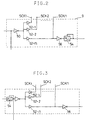
- Fig. 1 is a circuit diagram of a control circuit of a liquid crystal driver device in accordance with a first embodiment of the present invention.
- Fig. 2 is a circuit diagram showing one modification of the control circuit section shown in Fig. 1.
- Fig. 3 is a circuit diagram showing another modification of the control circuit section of Fig. 1.
- Fig. 4 is a circuit diagram of a signal-line driver circuit of the liquid crystal driver device in accordance with the first embodiment of the invention.
- Fig. 5 is a circuit diagram showing a modification of the signal-line driver circuit in Fig. 4.
- Fig. 6 is a circuit diagram showing another modification of the signal-line driver circuit in Fig. 4.
- Fig. 7 is a timing chart of respective signals in the first embodiment.
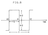
- Fig. 8 is a diagram for explanation of the duty ratio in accordance with the principles of the present invention.
- Fig. 9 is a circuit diagram of an analog PLL circuit.
- Fig. 10 is a circuit diagram of a digital PLL circuit.
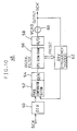
- Fig. 11 is a circuit diagram of a control circuit of a liquid crystal driver device in accordance with a second embodiment of the invention.
- Fig. 12 is a timing chart of respective signals in the second embodiment.
- Fig. 13 is a circuit diagram of a driver circuit of one prior known liquid crystal display device.
- Fig. 14 is a circuit diagram of a control circuit as provided in the prior art device.
- Fig. 15 is a timing chart of respective signals in the prior art.
- a driver circuit adaptable for use in an active-matrix liquid crystal display (LCD) device in accordance with a first embodiment of the present invention will now be described with reference to Figs. 1 through 10. Note here that the overall configuration of the active-matrix LCD device may be similar to that shown in Fig. 13.
- IC integrated circuit
- the control circuit 10 includes a horizontal clock signal generator circuit section 9 for generating and issuing a horizontal clock signal CK1 and phase-adjustment clock signals SCK, a signal generator circuit section 11 for producing several signals including a horizontal start signal ST, a vertical clock signal CK and a load signal LD, and for delaying them by a specified time interval, and a delay-time adjuster circuit section 14 for receiving RGB color image data items Data, which may be input as 8-bit digital signals, for example, and for delaying a respective one of these signals by a predefined time interval.
- FIG. 7 shows a timing chart of the horizontal clock signal CK1, horizontal start signal ST, image data Data, load signal LD and vertical clock signal CK2.
- the horizontal clock signal generator circuit section 9 is constituted from a phase inversion circuit 50 consisting of an inverter circuit that inverts by 180 degrees the phase of a reference clock signal CK as input thereto.
- the horizontal clock signal generator circuit section 9 also includes a predetermined number (n) of buffers 52-1, 52-2,..., 52-n that are parallel-connected to an output terminal of the phase inversion circuit 50 for generating and issuing adjustment clock signals SCK, each of which is supplied to a corresponding one of RGB latches 18R-1, 18G-1, 18B-1; 18R-2, 18G-2, 18B-2;...; 18R-n, 18G-n, 18B-n constituting the delay-time adjuster circuit section 14 and latches (these may be similar in configuration to those in the delay-time adjuster circuit section 14, and not shown here) of the signal generator circuit section 11.
- the final-stage latches 18R-n, 18G-n, 18B-n of the delay-time adjuster circuit section 14 and the output of buffer 52-n for control of the final-stage latches (not shown) in the signal generator circuit section 11 are connected to a phase-locked loop (PLL) circuit 54.
- PLL phase-locked loop
- This PLL circuit 54 has two output diverted: one output is connected to the final-stage latches 18R-n, 18G-n, 18B-n in delay-time adjuster circuit section 14 and the final-stage latches in signal generator circuit section 11; the other is tied to a phase inversion circuit 56 consisting of an inverter circuit or the like.
- This phase inversion circuit 56 generates at its output an inverted signal which is then sent forth from the control circuit 10 as the horizontal clock signal CK1.
- the delay-time adjuster circuit section 14 is arranged so that it includes a serial combination of n latches 18 as operatively coupled at its input to a corresponding one of R, G and B data items Data(R), Data(G), Data(B) of the color image data Data, and also coupled at the output of final-stage latch 18R-n, 18G-n or 18B-n to an amplifier 20 as shown.
- a corresponding row of latches 18R-1, 18R-2,..., 18R-n are connected in series thereto; for green (G) data, another row of latches 18G-1, 18G-2,..., 18G-n are series-connected thereto; and, for blue (B), the remaining row of latches 18B-1, 18B-2,..., 18B-n are series-coupled in a similar manner.
- the first buffer 52-1 issues a first adjustment clock signal SCK-1, which is then supplied in parallel to the individual one of the first-stage latches of respective RGB image data Data, that is, the latches 18R-1, 18G-1 and 18B-1. Hence, each latch 18 operates in response to the first adjustment clock signal SCK-1.
- each RGB image data Data is delayed by a predetermined time interval.
- n-th adjustment clock signal SCK-n fed from the PLL circuit 54 as discussed previously is input to the final-stage latches 18R-n, 18G-n, 18B-n forcing each RGB image data Data to be delayed in time so as to be synchronized with the horizontal clock signal CK1.
- control signals such as the horizontal start signal ST, vertical clock signal CK2 and load signal LD generated by the signal generator circuit section 11 are also delayed by a predetermined time interval based on each adjustment clock signal SCK such that the individual signal is in synchronization with the horizontal clock signal CK1.
- the PLL circuit as employed herein is defined as phase-locked loop circuit which provides an oscillation output that is kept constantly in phase and in frequency with an input signal thereof at any events, and which monitors and compares the oscillation output with the input signal to ensure that the duty ratio thereof is 50% while controlling its oscillator so that a difference between the both signals to be substantially zero (0) constantly.
- the horizontal clock signal CK1 is generated and the signal generator circuit section 11 and the final-stage latches 18R-n, 18G-n, 18B-n constituting the delay-time adjuster circuit section 14 is controlled.
- the horiozntal clock signal CK1 fed from the control circuit 10 is kept substantially in phase with respective image signals Data(R), Data(G), Data(B), horizontal start signal ST, vertical clock signal CK2, load signal LD and the like.
- the output from the PLL circuit 54 is or approximates 50% in duty ratio; therefore, as shown in the timing chart of Fig. 7, even where the RGB image signals Data are subject to sampling in signal-line driver circuit 24 by utilizing the timing of descending pulse edges of the horizontal clock signal CK1, it will no longer happen that the timing of sampling deviate significantly enabling achievement of reliable sampling of image signals Data even at extra-high operating speed.
- Another advantage of the illustrative circuit configuration is that even when the duty ratio of the incoming reference clock signal CK is much deviated from 50%, the duty ratio can be compensated for.
- Fig. 4 is a diagram showing a configuration of signal-line driver circuits 24 as employed in the LCD driver circuit embodying the present invention, wherein a plurality of signal-line driver circuits 24 are disposed and electrically connected.
- each signal-line driver circuit 24 typically includes a shift register section 26, a first latch section 28, a second latch section 30, and a plurality of driver circuit sections 32, all of which are integrated in the semiconductor chip.
- the shift register section 26 is connected to receive the horizontal start signal ST and horizontal clock signal CK1 as fed from the control circuit 10, whereas the first latch section 28 is to receive the RGB image data Data.
- the second latch section 30 receives the load signal LD from control circuit 10. Using these signals, image signals are produced which are supplied from the driver circuits 32 to the signal lines.
- the horizontal clock signal CK1 is input to the shift register section 26 via a PLL circuit 34 (as inserted into the clock-signal line).
- a PLL circuit 34 By passing through this PLL circuit 34, any possible distortion of waveform of the horizontal clock signal CK1 and deviation or "breakage" of the duty ratio thereof can be corrected enabling the horizontal clock signal to be input while being kept exactly in phase with RGB image data Data.
- respective signal-line driver circuits 24 are integrated in the semiconductor chip as an IC element while allowing the PLL circuit 34 to be operatively coupled in common to respective signal-line driver circuits 24 as a separate circuit component therefor, the present invention should not be limited exclusively to such configuration.
- the signal-line driver circuits 24 may be modified so that each comes with its exclusive PLL circuit 34 as integrally formed in the same semiconductor chip.
- the PLL circuit 34 may be added also to other signal transmission paths for the RGB image data Data, start signal ST and load signal LD, not only to the horizontal clock signal CK1.
- PLL circuits generally include analog PLL circuits and digital ones. Any one of such types may be employed as the PLL circuit(s) 34 in the illustrative embodiment.
- Digital PLL circuits can offer an largely increased time constant by supplying control while digitalizing phase comparison results between the input frequency and output frequency, averaging resultant phase difference data during time elapse of several seconds, and detecting extra low-frequency phase deviations alone, thereby lowering the jitter cutoff frequency. Further the duty ratio can easily be controlled at 50%.
- Fig. 9 shows one exemplary configuration of an analog PLL circuit 40, which includes a series combination of a phase comparator section 42, an analog filter 44, and a voltage-controlled oscillator (VCO) 46 as labelled by "VCXO" here, with an output thereof being fed back to the phase comparator section 42.
- VCO voltage-controlled oscillator
- Fig. 10 shows one exemplary configuration of a digital PLL circuit 48.
- This digital PLL circuit 48 includes a series connection of a frequency divider 50 as labelled “DIV” here, a phase comparator section 52, a digital-to-analog (D/A) converter 54, a digital filter 56, an analog-to-digital (A/D) converter 58, and a VCO 60 as labelled "VCXO" with its output being fed back to the phase comparator 52 through DIV 62.
- the digital filter 56 operates to preset DIV 62.
- the PLL circuit 54 is connected to the final-stage buffer 52-n; alternatively, the same may be provided on the output side of the phase inversion circuit 56 as shown in Fig. 2.
- the PLL circuit 54 is connected to the input of phase inversion circuit 50.
- the control operation of control circuit 10 may be facilitated because of the fact that wave-shaping is executed even where the duty ratio of an externally supplied reference clock signal CK is deviated from its intended value.
- the signal generator circuit section 11 does generate and issue several control signals including the start signal ST and load signal LD based on the reference clock signal CK with its duty ratio being compensated for by the PLL circuit 54. This essentially enables several kinds of signals to be exactly in phase with each other accomplishing excellent, high-quality/high-precision display images even in extra-high speed operation.
- the PLL circuit or circuits are employed for holding the duty ratio at 50%; however, zero-cross detectors or the like may alternatively be used therefor.
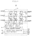
- control circuit 10 in accordance with a second embodiment of the present invention will now be described with reference to Fig. 11.
- the control circuit 10 is integrated as an IC element on a semiconductor chip substrate together with other elements as mounted thereon.
- the control circuit 10 includes a signal generator circuit section 12 which is responsive to receipt of a reference clock signal CK and synchronization signal EN as externally supplied from an outside personal computer or the like associated therewith, for generating and issuing the horizontal clock signal CK1, horizontal start signal ST, vertical clock signal CK2 and phase-adjustment clock signals SCK, and a delay-time adjuster circuit section 14 that operates to delay RGB image data Data by a predefined time interval.
- a combination of the horizontal clock signal generator circuit section 9 as used in the first embodiment and the signal generator circuit section 11 for production of several signals including the horizontal start signal ST, vertical clock signal CK2 and load signal LD is called the "signal generator circuit section 12."
- the signal generator circuit section 12 While the signal generator circuit section 12 generates and issues the adjustment clock signals SCK1, SCK2,..., SCKn that may each act as a reference signal for operation control of the delay-time adjuster circuit section 14, this circuit 12 does not directly provide such output signals SCK to the delay-time adjuster circuit section 14; rather, it provides the same thereto via respective PLL circuits 16-1, 16-2,..., 16-n shown.
- the delay-time adjuster circuit section 14 includes therein a plurality of latches 18 with each series combination of latches being connected to a corresponding one of RGB image data Data while allowing each color data output being sent forth via an amplifier 20.
- the latches 18 include a first row of latches 18R-1, 18R-2,..., 18R-n as series-connected to the red (R) image data Data(R).
- the latches 18 also include a second row of series-connected latches 18G-1, 18G-2,..., 18G-n for the green (G) image data Data(G), and a third row of series latches 18B-1, 18B-2,..., 18B-n for the blue (B) image data Data(B).
- the signal generator circuit section 12 generates a first adjustment clock signal SCK-1, which is corrected by its associated PLL circuit 16-1 providing a corrected first adjustment clock signal as labelled "SCK'-1.”
- This clock signal is then passed to an associative column or "first-stage” latches 18R-1, 18G-1, 18B-1, and further to the signal generator circuit section 12 in a parallel manner, causing a respective one of these first-stage latches 18R-1, 18G-1, 18B-1 to operate in response to such PLL-corrected first adjustment clock signal SCK'-1.
- Providing the PLL circuit 16-1 may ensure that even where three latches 18R-1, 18G-1, 18B-1 are parallel-connected, the first adjustment clock signal SCK'-1 will no longer be out of phase without being adversely affected therefrom. Consequently, it makes it possible for RGB image data Data to be kept exactly in phase with the first adjustment clock signal SCK-1.
- the second-stage latch set 18R-2, 18G-2, 18B-2 since a second adjustment clock signal SCK-2 is input thereto via a PLL circuit 16-2, accurate phase adjustment or "synchronization control" can be accomplished letting the RGB image data be exactly in phase with the second adjustment clock signal. The same is true for the remaining, third to final-stage latches, enabling by adequate PLL-phase correction achievement of accurate synchronization between each stage latch set and its associated adjustment clock signal SCK.
- PLL circuits 16 as employed in the control circuit 10 and the signal-line driver circuits 24 connected to the control circuit 10 may be similar in configuration to those as used in the first embodiment as discussed previously.
- a display device capable of achieving accurate sampling of image data even where the operation speed is increased to attain extra-high precision image display schemes thereby enabling accomplishment of excellent, high-quality display images thereon.
Abstract
A display comprises a liquid crystal panel, a signal line driver circuit for generating a signal, which is to be supplied to a signal line, on the basis of image data and a first clock signal CK1, a control signal generating circuit (12) for generating the first clock signal CK1 and a regulating clock signal SCK on the basis of a reference clock signal, and a delay time regulating circuit (14) for delaying data by a predetermined time on the basis of the regulating clock signal SCK from the control signal generating circuit (12) for the purpose of regulating the delay time of the first clock signal CK1 generated with respect to the data by the control signal generating circuit (12). The delay time regulating circuit (14) is provided with a PLL circuit (16) for correcting the regulating clock signal SCK, and a PLL circuit (34) for correcting the first clock signal CK1 supplied to the signal line driver circuit, whereby the phase of the first clock signal CK1 and that of the data are accurately set in agreement with each other.
Description
- The present invention relates generally to display devices with an optical modulation layer such as a liquid crystal layer, and more particularly to liquid crystal display (LCD) devices.
- Fig. 13 is a diagram showing a configuration of driver circuit of an active-matrix LCD device.
-
Numeral 102 designates an LCD panel which is constituted from a first electrode substrate having a plurality of pixel electrodes as arranged in a matrix form, for example, a second electrode substrate with an opposed electrode opposing the pixel electrodes, and a liquid crystal provided as an optical modulation layer disposed between these first and second electrode substrates through orientation films. - Numeral 104 designates a predetermined number of signal-line driver circuits each of which output an image signal, to the signal lines connected to the pixel electrodes, via switching elements such as a thin-film transistor (referred to as "TFT" hereinafter), of the
LCD panel 102. -
Numeral 108 indicates a scanning-line driver circuit which serves to output a scanning signal to the scanning lines for control of switching element being electrically connected to the pixel electrodes ofLCD panel 102. -
Numeral 110 is a control circuit which generates and supplies several signals, including image data Data, a horizontal clock signal CK1 and a start signal ST, to the signal-line driver circuits 104, and which generates and supplies several signals including a vertical clock signal CK2 to the scanning-line driver circuit 108. - This
control circuit 110 will now be described in detail with reference to Fig. 9. - The
control circuit 110 comprises a horizontal clock signalgenerator circuit section 109, a signalgenerator circuit section 112, and a delay timeadjuster circuit section 113. - The horizontal clock signal
generator circuit section 109 generates the horizontal clock signal CK1 and an adjustment clock signal SCK based on a reference clock signal CK as provided from an external unit operatively associated therewith, such as a personal computer or the like. - The delay time adjuster circuit section adjust the phase of image data Data and the horizontal clock signal CK1 to each other to delay the time of generating the horizontal clock signal CK1 by the horizontal clock signal
generator circuit section 109, when image data of red (R), green (G) and blue (B) components (referred to as "RGB" hereinafter) are input from outside. A circuit configuration thereof is such that latch circuits 114 are connected in series to signal lines of transmission of respective RGB image data Data while constructing multiple stages therein, enabling the image data Data to delay due to operation of latches 114. This delayed time can be adjusted in response to receipt of the adjustment clock signal SCK which is fed from the horizontal clock signalgenerator circuit section 109 to each stage of latch 114. - The signal
generator circuit section 112 is responsive to receipt of a synchronization signal EN and reference clock signal CK provided by the external unit such as the personal computer, for generating and issuing the vertical clock signal CK2, horizontal start signal ST and others. - The signal
generator circuit section 112 also delay the timing of the generated signals, including the vertical clock signal CK2 and horizontal start signal ST, based on the adjustment clock signal SCK which is defined by the time lag for generating the horizontal clock signal CK1 by the horizontal clock signalgenerator circuit section 109, and adjust the phase of generated signals and the horizontal clock signals CK1 to each other, in a manner similar to that of the delay time adjuster circuit. - The operation of the driver circuit 100 thus arranged is as follows.
- The RGB image data Data, synchronization signal EN and reference clock signal CK are input to the
control circuit 110. In responding, the horizontal clock signalgenerator circuit section 109 and signalgenerator circuit section 112 generate and issue the horizontal clock signal CK1, vertical clock signal CK2 and horizontal start signal ST or the like while outputting the adjustment clock signal SCK to respective latches 114 of the delay timeadjuster circuit section 113, thus effecting phase adjustment between RGB image data Data and horizontal clock signal CK1. - In the signal-
line driver circuit 104 an image signal is generated based on the horizontal clock signal CK1, horizontal start signal ST, image data Data and load signal LD to be output to each of the signal lines of theLCD panel 102. - In the scanning-line driver circuit 108 a scanning signal is generated based on the vertical clock signal CK2 for supplement to the scanning lines of the
LCD panel 102. - Fig. 15 shows a timing chart of the horizontal clock signal CK1, horizontal start signal ST, load signal LD and vertical clock signal CK2.
- The prior known driver circuit 100 mentioned suffers from several problems as will be set forth below.
- (1) While the reference clock signal CK externally supplied thereto is passing through circuit elements such as a phase inversion circuit as provided in the horizontal clock signal
generator circuit section 109, it will possibly happen that the duty ratio of reference clock signal CK is deviated. If this is the case, the duty ratio of the horizontal clock signal CK1 fed to the signal-line driver circuit 104 can also be deviated accordingly. Especially, in cases where aphase inversion circuit 150 is disposed at a subsequent node of the output of the final-stage adjustment clock signal SCKn as in thecontrol circuit 110 of Fig. 14, resultant sampling of RGB image signal Data should be carried out utilizing the timing of the falling pulse edge of horizontal clock signal CK1 as demonstrated in the timing chart of Fig. 15. When this is done, if the duty ratio is deviated, the sampling will also deviate in timing causing the set-up time to become insufficient, which in turn leads to the risk of sampling of different image signals Data. - (2) While in the
control circuit 110 the horizontal clock signalgenerator circuit section 109 supplies the adjustment clock signal SCK to the latches 114 of the delay timeadjuster circuit section 113 and the signalgenerator circuit section 112, since these latches 114 are a parallel combination of plural sets of RGB latches, the adjustment clock signal SCK will be supplied to these latches 114 in a parallel signal transmission manner. This can adversely serve to cause such parallel-feed adjustment clock signals SCK to deviate in phase due to undesired distortion in waveform thereof as raised by the presence of inherent capacitance in the latches 114, leading to a problem in that phase deviation arises letting the RGB image data Data, horizontal clock signal CK1 and horizontal start signal ST be out of phase with the load signal LD or the like. - (3) A further problem is that where the horizontal clock signal CK1 alike and the RGB image data Data are input to the signal-
line driver circuit 104, the waveforms thereof can deviate under adverse interference with their associated wiring-line paths and internal circuits of the signal-line driver circuit 104 causing the phase to deviate between them. - After all, due to the aforesaid problems (1) to (3), several kinds of signals will possibly deviate in phase in the timing chart of Fig. 15. In particular, the horizontal clock signal CK1 and image data Data become different in phase from the vertical clock signal CK2 and horizontal start signal ST; if this once happens, since their periods are relatively narrow, the phase focussing can easily be out of work resulting in deviations in phase among them. This will become more serious as the operation speed is much increased to attain extra-high precision image display schemes as demanded endlessly in the art to which the invention pertains.
- It is therefore an object of the present invention to provide an improved display device capable of attaining accurate sampling of image data even where the operation speed is increased to achieve such extra-high precision image display schemes thereby enabling accomplishment of excellent, high-quality display images thereon.
- In accordance with a first principle of the present invention, a display device includes a display panel having a plurality of display pixels electrically connected to a plurality of signal lines, a control circuit which includes clock signal generator means responsive to receipt of an input reference clock signal for generating based thereon a first clock signal and a phase-adjustment clock signal and phase adjuster means for adjusting based on the adjustment clock signal the relation in phase between input image data and the first clock signal, and a signal-line driver circuit for providing an image signal to the signal lines based on at least the image data and the first clock signal, featured in that the clock signal generator means includes therein a duty-ratio adjuster circuit for correcting the duty ratio of the first clock signal being output to the signal-line driver circuit so that the ratio is approximately 50 percent (%).
- With such an arrangement, since the duty ratio of the first clock signal being output to the signal-line driver circuit is corrected to be approximately 50%, even where the operation speed is increased to attain high precision, accurate image-data sampling can be accomplished enabling achievement of excellent display images with enhanced quality.
- In accordance with a second principle of the invention, a display device includes a display panel having a plurality of display pixels electrically connected to a plurality of signal lines, a control circuit including clock signal generator means responsive to an incoming reference clock signal for generating a first clock signal and an adjustment clock signal and phase adjuster means for adjusting based on the adjustment clock signal the relation in phase between input image data and the first clock signal, and a signal-line driver circuit for providing an image signal to the signal lines based on at least the image data and the first clock signal, featured in that the clock signal generator means and the phase adjuster means are connected to each other through a PLL circuit for the adjustment clock signal.
- With the arrangement also, accurate image-data sampling can be achieved providing high-quality display images.
- In accordance with a third principle of the invention, a display device includes a display panel having a plurality of display pixels electrically connected to a plurality of signal lines, a control circuit section for output of image data, a first clock signal and a control signal, and a signal-line driver circuit for supplying an image signal to the signal lines based on the image data and the control signal, featured in that the signal-line driver circuit includes first phase adjuster means on the input side of at least one of the image data, the first clock signal and the control signal.
- It thus becomes possible, by providing the signal-line driver circuit with the first phase adjuster means disposed therein also, to achieve accurate image-data sampling attaining excellent display images.
- In accordance with a fourth principle of the invention, a display device includes a display panel having a plurality of display pixels electrically connected to a plurality of signal lines, a control circuit including clock signal generator means responsive to an input reference clock signal for generating a first clock signal and an adjustment clock signal and phase adjuster means for adjusting based on the adjustment clock signal the relation in phase between the first clock signal and one of input image data and a control signal, and a signal-line driver circuit for providing an image signal to the signal lines based on the image data, the first clock signal and the control signal, featured in that the clock signal generator means includes therein a built-in duty-ratio adjuster circuit for correction of the duty ratio of the first clock signal being output to the signal-line driver circuit so that the ratio is approximately 50%.
- Fig. 1 is a circuit diagram of a control circuit of a liquid crystal driver device in accordance with a first embodiment of the present invention.
- Fig. 2 is a circuit diagram showing one modification of the control circuit section shown in Fig. 1.
- Fig. 3 is a circuit diagram showing another modification of the control circuit section of Fig. 1.
- Fig. 4 is a circuit diagram of a signal-line driver circuit of the liquid crystal driver device in accordance with the first embodiment of the invention.
- Fig. 5 is a circuit diagram showing a modification of the signal-line driver circuit in Fig. 4.
- Fig. 6 is a circuit diagram showing another modification of the signal-line driver circuit in Fig. 4.
- Fig. 7 is a timing chart of respective signals in the first embodiment.
- Fig. 8 is a diagram for explanation of the duty ratio in accordance with the principles of the present invention.
- Fig. 9 is a circuit diagram of an analog PLL circuit.
- Fig. 10 is a circuit diagram of a digital PLL circuit.
- Fig. 11 is a circuit diagram of a control circuit of a liquid crystal driver device in accordance with a second embodiment of the invention.
- Fig. 12 is a timing chart of respective signals in the second embodiment.
- Fig. 13 is a circuit diagram of a driver circuit of one prior known liquid crystal display device.
- Fig. 14 is a circuit diagram of a control circuit as provided in the prior art device.
- Fig. 15 is a timing chart of respective signals in the prior art.
- A driver circuit adaptable for use in an active-matrix liquid crystal display (LCD) device in accordance with a first embodiment of the present invention will now be described with reference to Figs. 1 through 10. Note here that the overall configuration of the active-matrix LCD device may be similar to that shown in Fig. 13.
- Referring now to Fig. 1, there is shown a circuit configuration of a
control circuit 10 as employed in the driver circuit of this embodiment, wherein thecontrol circuit 10 is integrally arranged in a semiconductor chip as an integrated circuit (IC) element. - The
control circuit 10 includes a horizontal clock signalgenerator circuit section 9 for generating and issuing a horizontal clock signal CK1 and phase-adjustment clock signals SCK, a signalgenerator circuit section 11 for producing several signals including a horizontal start signal ST, a vertical clock signal CK and a load signal LD, and for delaying them by a specified time interval, and a delay-timeadjuster circuit section 14 for receiving RGB color image data items Data, which may be input as 8-bit digital signals, for example, and for delaying a respective one of these signals by a predefined time interval. - See Fig. 7, which shows a timing chart of the horizontal clock signal CK1, horizontal start signal ST, image data Data, load signal LD and vertical clock signal CK2.
- The horizontal clock signal
generator circuit section 9 is constituted from aphase inversion circuit 50 consisting of an inverter circuit that inverts by 180 degrees the phase of a reference clock signal CK as input thereto. The horizontal clock signalgenerator circuit section 9 also includes a predetermined number (n) of buffers 52-1, 52-2,..., 52-n that are parallel-connected to an output terminal of thephase inversion circuit 50 for generating and issuing adjustment clock signals SCK, each of which is supplied to a corresponding one of RGB latches 18R-1, 18G-1, 18B-1; 18R-2, 18G-2, 18B-2;...; 18R-n, 18G-n, 18B-n constituting the delay-timeadjuster circuit section 14 and latches (these may be similar in configuration to those in the delay-timeadjuster circuit section 14, and not shown here) of the signalgenerator circuit section 11. The final-stage latches 18R-n, 18G-n, 18B-n of the delay-timeadjuster circuit section 14 and the output of buffer 52-n for control of the final-stage latches (not shown) in the signalgenerator circuit section 11 are connected to a phase-locked loop (PLL)circuit 54. ThisPLL circuit 54 has two output diverted: one output is connected to the final-stage latches 18R-n, 18G-n, 18B-n in delay-timeadjuster circuit section 14 and the final-stage latches in signalgenerator circuit section 11; the other is tied to aphase inversion circuit 56 consisting of an inverter circuit or the like. Thisphase inversion circuit 56 generates at its output an inverted signal which is then sent forth from thecontrol circuit 10 as the horizontal clock signal CK1. - The delay-time
adjuster circuit section 14 is arranged so that it includes a serial combination of n latches 18 as operatively coupled at its input to a corresponding one of R, G and B data items Data(R), Data(G), Data(B) of the color image data Data, and also coupled at the output of final-stage latch 18R-n, 18G-n or 18B-n to anamplifier 20 as shown. For instance, upon receipt of incoming red (R) data item of the image data Data, a corresponding row oflatches 18R-1, 18R-2,..., 18R-n are connected in series thereto; for green (G) data, another row oflatches 18G-1, 18G-2,..., 18G-n are series-connected thereto; and, for blue (B), the remaining row oflatches 18B-1, 18B-2,..., 18B-n are series-coupled in a similar manner. - In the horizontal clock signal
generator circuit section 9 the first buffer 52-1 issues a first adjustment clock signal SCK-1, which is then supplied in parallel to the individual one of the first-stage latches of respective RGB image data Data, that is, thelatches 18R-1, 18G-1 and 18B-1. Hence, each latch 18 operates in response to the first adjustment clock signal SCK-1. - Similarly, also in each stage of latch 18 other than the final-stage one, a corresponding adjustment clock signal SCK is input causing each RGB image data Data to be delayed by a predetermined time interval.
- Further, the n-th adjustment clock signal SCK-n fed from the
PLL circuit 54 as discussed previously is input to the final-stage latches 18R-n, 18G-n, 18B-n forcing each RGB image data Data to be delayed in time so as to be synchronized with the horizontal clock signal CK1. - In a manner similar to that of each RGB image data, several control signals such as the horizontal start signal ST, vertical clock signal CK2 and load signal LD generated by the signal
generator circuit section 11 are also delayed by a predetermined time interval based on each adjustment clock signal SCK such that the individual signal is in synchronization with the horizontal clock signal CK1. - The PLL circuit as employed herein is defined as phase-locked loop circuit which provides an oscillation output that is kept constantly in phase and in frequency with an input signal thereof at any events, and which monitors and compares the oscillation output with the input signal to ensure that the duty ratio thereof is 50% while controlling its oscillator so that a difference between the both signals to be substantially zero (0) constantly.
- Here, the duty ratio is defined as follows. See Fig. 8, in the waveform of a pulse signal, when time points t0, t1, t2 is defined as "zero-cross" points or 1/2 of the amplitude A, T0 is defined as


- With the
control circuit 10 thus arranged, based on an output of thePLL circuit section 54, the horizontal clock signal CK1 is generated and the signalgenerator circuit section 11 and the final-stage latches 18R-n, 18G-n, 18B-n constituting the delay-timeadjuster circuit section 14 is controlled. For this reason, the horiozntal clock signal CK1 fed from thecontrol circuit 10 is kept substantially in phase with respective image signals Data(R), Data(G), Data(B), horizontal start signal ST, vertical clock signal CK2, load signal LD and the like. - Further, the output from the
PLL circuit 54 is or approximates 50% in duty ratio; therefore, as shown in the timing chart of Fig. 7, even where the RGB image signals Data are subject to sampling in signal-line driver circuit 24 by utilizing the timing of descending pulse edges of the horizontal clock signal CK1, it will no longer happen that the timing of sampling deviate significantly enabling achievement of reliable sampling of image signals Data even at extra-high operating speed. - Another advantage of the illustrative circuit configuration is that even when the duty ratio of the incoming reference clock signal CK is much deviated from 50%, the duty ratio can be compensated for.
- Fig. 4 is a diagram showing a configuration of signal-
line driver circuits 24 as employed in the LCD driver circuit embodying the present invention, wherein a plurality of signal-line driver circuits 24 are disposed and electrically connected. As shown in Fig. 4, for example, each signal-line driver circuit 24 typically includes ashift register section 26, afirst latch section 28, asecond latch section 30, and a plurality ofdriver circuit sections 32, all of which are integrated in the semiconductor chip. Theshift register section 26 is connected to receive the horizontal start signal ST and horizontal clock signal CK1 as fed from thecontrol circuit 10, whereas thefirst latch section 28 is to receive the RGB image data Data. Thesecond latch section 30 receives the load signal LD fromcontrol circuit 10. Using these signals, image signals are produced which are supplied from thedriver circuits 32 to the signal lines. - While the horizontal start signal ST and RGB image data Data are directly input to the
shift register section 26 andfirst latch section 28, the horizontal clock signal CK1 is input to theshift register section 26 via a PLL circuit 34 (as inserted into the clock-signal line). By passing through thisPLL circuit 34, any possible distortion of waveform of the horizontal clock signal CK1 and deviation or "breakage" of the duty ratio thereof can be corrected enabling the horizontal clock signal to be input while being kept exactly in phase with RGB image data Data. - With such an arrangement, even where the display operation increases in speed while having the horizontal clock signal CK1 and RGB image data Data increased in frequency with the period decreased, it becomes possible to suppress or eliminate degradation of the horizontal clock signal CK1 and deviation of the duty ratio thereof otherwise occurring due to adverse influence with the time constant as defined by inherent parasitic or stary capacitances on wiring lines, to ensure that the both can be exactly in phase with each other constantly. This advantageously serves to achieve accurate, high-speed synchronization in liquid crystal driving schemes, which in turn leads to the possibility of providing extra large-size LCD devices.
- Although in the illustrative embodiment respective signal-
line driver circuits 24 are integrated in the semiconductor chip as an IC element while allowing thePLL circuit 34 to be operatively coupled in common to respective signal-line driver circuits 24 as a separate circuit component therefor, the present invention should not be limited exclusively to such configuration. By way of example, as shown in Fig. 5, the signal-line driver circuits 24 may be modified so that each comes with itsexclusive PLL circuit 34 as integrally formed in the same semiconductor chip. - Alternatively, as shown in Fig. 6, the
PLL circuit 34 may be added also to other signal transmission paths for the RGB image data Data, start signal ST and load signal LD, not only to the horizontal clock signal CK1. - PLL circuits generally include analog PLL circuits and digital ones. Any one of such types may be employed as the PLL circuit(s) 34 in the illustrative embodiment. Digital PLL circuits can offer an largely increased time constant by supplying control while digitalizing phase comparison results between the input frequency and output frequency, averaging resultant phase difference data during time elapse of several seconds, and detecting extra low-frequency phase deviations alone, thereby lowering the jitter cutoff frequency. Further the duty ratio can easily be controlled at 50%.
- Fig. 9 shows one exemplary configuration of an
analog PLL circuit 40, which includes a series combination of aphase comparator section 42, ananalog filter 44, and a voltage-controlled oscillator (VCO) 46 as labelled by "VCXO" here, with an output thereof being fed back to thephase comparator section 42. In this case, as the accuracy ofVCXO 46 increases, controlling of the duty ratio at 50% may become easier accordingly. - Fig. 10 shows one exemplary configuration of a
digital PLL circuit 48. Thisdigital PLL circuit 48 includes a series connection of afrequency divider 50 as labelled "DIV" here, aphase comparator section 52, a digital-to-analog (D/A)converter 54, adigital filter 56, an analog-to-digital (A/D)converter 58, and aVCO 60 as labelled "VCXO" with its output being fed back to thephase comparator 52 throughDIV 62. Thedigital filter 56 operates to presetDIV 62. - In the
control circuit 10 of Fig. 1 thePLL circuit 54 is connected to the final-stage buffer 52-n; alternatively, the same may be provided on the output side of thephase inversion circuit 56 as shown in Fig. 2. - Another possible modification is that as shown in Fig. 3, the
PLL circuit 54 is connected to the input ofphase inversion circuit 50. In this case, the control operation ofcontrol circuit 10 may be facilitated because of the fact that wave-shaping is executed even where the duty ratio of an externally supplied reference clock signal CK is deviated from its intended value. Especially, with such an arrangement, the signalgenerator circuit section 11 does generate and issue several control signals including the start signal ST and load signal LD based on the reference clock signal CK with its duty ratio being compensated for by thePLL circuit 54. This essentially enables several kinds of signals to be exactly in phase with each other accomplishing excellent, high-quality/high-precision display images even in extra-high speed operation. - In the foregoing embodiment the PLL circuit or circuits are employed for holding the duty ratio at 50%; however, zero-cross detectors or the like may alternatively be used therefor.
- A
control circuit 10 in accordance with a second embodiment of the present invention will now be described with reference to Fig. 11. In this embodiment also, thecontrol circuit 10 is integrated as an IC element on a semiconductor chip substrate together with other elements as mounted thereon. - As shown in Fig. 11, the
control circuit 10 includes a signal generator circuit section 12 which is responsive to receipt of a reference clock signal CK and synchronization signal EN as externally supplied from an outside personal computer or the like associated therewith, for generating and issuing the horizontal clock signal CK1, horizontal start signal ST, vertical clock signal CK2 and phase-adjustment clock signals SCK, and a delay-timeadjuster circuit section 14 that operates to delay RGB image data Data by a predefined time interval. In this embodiment, a combination of the horizontal clock signalgenerator circuit section 9 as used in the first embodiment and the signalgenerator circuit section 11 for production of several signals including the horizontal start signal ST, vertical clock signal CK2 and load signal LD is called the "signal generator circuit section 12." - While the signal generator circuit section 12 generates and issues the adjustment clock signals SCK1, SCK2,..., SCKn that may each act as a reference signal for operation control of the delay-time
adjuster circuit section 14, this circuit 12 does not directly provide such output signals SCK to the delay-timeadjuster circuit section 14; rather, it provides the same thereto via respective PLL circuits 16-1, 16-2,..., 16-n shown. - The delay-time
adjuster circuit section 14 includes therein a plurality of latches 18 with each series combination of latches being connected to a corresponding one of RGB image data Data while allowing each color data output being sent forth via anamplifier 20. In other words, the latches 18 include a first row oflatches 18R-1, 18R-2,..., 18R-n as series-connected to the red (R) image data Data(R). The latches 18 also include a second row of series-connectedlatches 18G-1, 18G-2,..., 18G-n for the green (G) image data Data(G), and a third row of series latches 18B-1, 18B-2,..., 18B-n for the blue (B) image data Data(B). - The signal generator circuit section 12 generates a first adjustment clock signal SCK-1, which is corrected by its associated PLL circuit 16-1 providing a corrected first adjustment clock signal as labelled "SCK'-1." This clock signal is then passed to an associative column or "first-stage" latches 18R-1, 18G-1, 18B-1, and further to the signal generator circuit section 12 in a parallel manner, causing a respective one of these first-stage latches 18R-1, 18G-1, 18B-1 to operate in response to such PLL-corrected first adjustment clock signal SCK'-1. Providing the PLL circuit 16-1 may ensure that even where three
latches 18R-1, 18G-1, 18B-1 are parallel-connected, the first adjustment clock signal SCK'-1 will no longer be out of phase without being adversely affected therefrom. Consequently, it makes it possible for RGB image data Data to be kept exactly in phase with the first adjustment clock signal SCK-1. - Similarly, regarding the second-stage latch set 18R-2, 18G-2, 18B-2 also, since a second adjustment clock signal SCK-2 is input thereto via a PLL circuit 16-2, accurate phase adjustment or "synchronization control" can be accomplished letting the RGB image data be exactly in phase with the second adjustment clock signal. The same is true for the remaining, third to final-stage latches, enabling by adequate PLL-phase correction achievement of accurate synchronization between each stage latch set and its associated adjustment clock signal SCK.
- It should be noted that the
PLL circuits 16 as employed in thecontrol circuit 10 and the signal-line driver circuits 24 connected to thecontrol circuit 10 may be similar in configuration to those as used in the first embodiment as discussed previously. - In accordance with the present invention, there can be provided a display device capable of achieving accurate sampling of image data even where the operation speed is increased to attain extra-high precision image display schemes thereby enabling accomplishment of excellent, high-quality display images thereon.
Claims (12)
- A display device comprising:a display panel having a plurality of display picture elements electrically connected to a plurality of signal lines;a control circuit including clock signal generator means responsive to an input reference clock signal for generating a first clock signal and an adjustment clock signal, and phase adjuster means for adjusting based on said adjustment clock signal relation in phase between input image data and said first clock signal; anda signal line driver circuit for providing an image signal to the signal lines based on at least said image data and said first clock signal, whereinsaid clock signal generator means includes a duty ratio adjuster circuit for correction of a duty ratio of said first clock signal being output to said signal line driver circuit so that said ratio is substantially 50 percent (%).
- The display device according to claim 1, wherein said duty ratio adjuster circuit is in a path for generation of said first clock signal in said clock signal generator means and is arranged near an output position along said path at which position said first clock signal is output.
- The display device according to claim 1, wherein said duty ratio adjuster circuit is arranged near an input position in said clock signal generator means at which position said reference clock signal is input.
- The display device according to claim 1, wherein said duty ratio adjuster circuit is a phase locked loop (PLL) circuit.
- A display device comprising:a display panel having a plurality of display picture elements electrically connected to a plurality of signal lines;a control circuit including clock signal generator means responsive to an input reference clock signal for generating a first clock signal and an adjustment clock signal, and phase adjuster means for adjusting based on said adjustment clock signal relation in phase between input image data and said first clock signal; anda signal line driver circuit for providing an image signal to the signal lines based on at least said image data and said first clock signal, whereinsaid clock signal generator means and said phase adjuster means are connected to each other through a PLL circuit operatively coupled to the adjustment clock signal.
- The display device according to claim 5, wherein said phase adjuster means includes a series combination of a plurality of delay circuits as controlled based on said adjustment clock signal while said delay circuits define multiple stages, and that each said delay circuit is associated with the PLL circuit for adjustment clock signal as disposed on an input side of said adjustment clock signal.
- A display device comprising:a display panel having a plurality of display picture elements electrically connected to a plurality of signal lines;a control circuit section for output of image data, a first clock signal and a control signal; anda signal line driver circuit for supplying an image signal to the signal lines based on said image data and said control signal, whereinsaid signal line driver circuit includes first phase adjuster means at an input of at least one of said image data, said first clock signal and said control signal.
- The display device according to claim 7, wherein said phase adjuster means is a duty ratio adjuster circuit for correcting a duty ratio so that the duty ratio is approximately 50%.
- The display device according to claim 7, wherein said phase adjuster means is a PLL circuit.
- The display device according to claim 7, wherein said control circuit section includes clock signal generator means for generating from an incoming reference clock signal a first clock signal and an adjustment clock signal, and second phase adjuster means for adjusting relation in phase of said first clock signal and image data as input thereto based on said adjustment clock signal, and that
said clock signal generator means includes a duty ratio adjuster circuit for correcting a duty ratio of said first clock signal being output to said signal line driver circuit so that the duty ratio is approximately 50%. - The display device according to claim 7, wherein said signal line driver circuit integrally includes said first phase adjuster means.
- A display device comprising:a display panel having a plurality of display picture elements electrically connected to a plurality of signal lines;a control circuit including clock signal generator means responsive to a reference clock signal as input thereto for generating a first clock signal and an adjustment clock signal, and phase adjuster means for adjusting based on said adjustment clock signal relation in phase between said first clock signal and one of incoming input image data and a control signal; anda signal line driver circuit for providing an image signal to the signal lines based on said image data, said first clock signal and said control signal, whereinsaid clock signal generator means includes a duty ratio adjuster circuit for correction of a duty ratio of said first clock signal being output to said signal line driver circuit so that said duty ratio is substantially 50%.13. The display device according to claim 12, wherein said duty ratio adjuster circuit is in a path for generation of said first clock signal in said clock signal generator means and is arranged near an output position along said path at which position said first clock signal is output.14. The display device according to claim 12, wherein said duty ratio adjuster circuit is arranged near an input position in said clock signal generator means at which position said reference clock signal is input.15. The display device according to claim 12, wherein said duty ratio adjuster circuit is a PLL circuit.
Applications Claiming Priority (3)
| Application Number | Priority Date | Filing Date | Title |
|---|---|---|---|
| JP26691095 | 1995-10-16 | ||
| JP266910/95 | 1995-10-16 | ||
| PCT/JP1996/002979 WO1997015041A1 (en) | 1995-10-16 | 1996-10-15 | Display |
Publications (2)
| Publication Number | Publication Date |
|---|---|
| EP0803856A1 true EP0803856A1 (en) | 1997-10-29 |
| EP0803856A4 EP0803856A4 (en) | 1999-12-08 |
Family
ID=17437371
Family Applications (1)
| Application Number | Title | Priority Date | Filing Date |
|---|---|---|---|
| EP96933645A Withdrawn EP0803856A4 (en) | 1995-10-16 | 1996-10-15 | Display |
Country Status (5)
| Country | Link |
|---|---|
| US (1) | US6144355A (en) |
| EP (1) | EP0803856A4 (en) |
| KR (1) | KR100230473B1 (en) |
| TW (1) | TW324067B (en) |
| WO (1) | WO1997015041A1 (en) |
Cited By (1)
| Publication number | Priority date | Publication date | Assignee | Title |
|---|---|---|---|---|
| DE102006016080A1 (en) * | 2006-04-04 | 2007-10-18 | Küster Automotive Door Systems GmbH | Power supply device for a plurality of consumers to be connected thereto |
Families Citing this family (20)
| Publication number | Priority date | Publication date | Assignee | Title |
|---|---|---|---|---|
| TW575196U (en) * | 1996-09-24 | 2004-02-01 | Toshiba Electronic Eng | Liquid crystal display device |
| US5796392A (en) | 1997-02-24 | 1998-08-18 | Paradise Electronics, Inc. | Method and apparatus for clock recovery in a digital display unit |
| JP3385301B2 (en) * | 1997-04-23 | 2003-03-10 | シャープ株式会社 | Data signal line drive circuit and image display device |
| JPH117268A (en) * | 1997-06-18 | 1999-01-12 | Sony Corp | Sample-and-hold circuit |
| US6538648B1 (en) * | 1998-04-28 | 2003-03-25 | Sanyo Electric Co., Ltd. | Display device |
| US6288699B1 (en) * | 1998-07-10 | 2001-09-11 | Sharp Kabushiki Kaisha | Image display device |
| US6535193B1 (en) * | 1998-10-02 | 2003-03-18 | Canon Kabushiki Kaisha | Display apparatus |
| JP3469116B2 (en) * | 1999-01-28 | 2003-11-25 | シャープ株式会社 | Display driving device and liquid crystal module using the same |
| US6611247B1 (en) * | 1999-07-01 | 2003-08-26 | Himax Technologies, Inc. | Data transfer system and method for multi-level signal of matrix display |
| KR100563826B1 (en) * | 1999-08-21 | 2006-04-17 | 엘지.필립스 엘시디 주식회사 | Data driving circuit of liquid crystal display |
| JP2001075524A (en) * | 1999-09-03 | 2001-03-23 | Rohm Co Ltd | Display device |
| JP3827917B2 (en) | 2000-05-18 | 2006-09-27 | 株式会社日立製作所 | Liquid crystal display device and semiconductor integrated circuit device |
| JP2002189456A (en) * | 2000-12-20 | 2002-07-05 | Fujitsu Ltd | Liquid crystal display device |
| TW200405258A (en) * | 2002-08-28 | 2004-04-01 | Matsushita Electric Ind Co Ltd | Data driver |
| US7271788B2 (en) * | 2003-11-20 | 2007-09-18 | National Semiconductor Corporation | Generating adjustable-delay clock signal for processing color signals |
| US7830348B2 (en) * | 2003-12-11 | 2010-11-09 | Au Optronics Corporation | Integrated circuit for liquid crystal display device |
| US7564454B1 (en) * | 2004-12-06 | 2009-07-21 | National Semiconductor Corporation | Methods and displays having a self-calibrating delay line |
| JP2008309896A (en) * | 2007-06-12 | 2008-12-25 | Toshiba Corp | Liquid crystal driver and liquid crystal display device |
| KR101580897B1 (en) * | 2008-10-07 | 2015-12-30 | 삼성전자주식회사 | Display driver method thereof and device having the display driver |
| KR101607155B1 (en) * | 2008-12-26 | 2016-03-30 | 삼성디스플레이 주식회사 | Display apparatus and method for driving the same |
Citations (2)
| Publication number | Priority date | Publication date | Assignee | Title |
|---|---|---|---|---|
| EP0577841A1 (en) * | 1992-01-23 | 1994-01-12 | Fanuc Ltd. | Circuit for controlling phase of video signal |
| DE4438426A1 (en) * | 1993-10-28 | 1995-05-04 | Sharp Kk | Display driver and data-transmission method |
Family Cites Families (12)
| Publication number | Priority date | Publication date | Assignee | Title |
|---|---|---|---|---|
| JPS5921045B2 (en) * | 1978-12-20 | 1984-05-17 | 富士通株式会社 | Adjustment method of clock signal distribution circuit |
| US4275421A (en) * | 1979-02-26 | 1981-06-23 | The United States Of America As Represented By The Secretary Of The Navy | LCD controller |
| US4580165A (en) * | 1984-04-12 | 1986-04-01 | General Electric Company | Graphic video overlay system providing stable computer graphics overlayed with video image |
| US4688081A (en) * | 1985-01-25 | 1987-08-18 | Hitachi, Ltd. | Apparatus for correcting time base error of video signal |
| US5157773A (en) * | 1986-03-14 | 1992-10-20 | Canon Kabushiki Kaisha | Image data output apparatus |
| US4782391A (en) * | 1987-08-19 | 1988-11-01 | Rca Licensing Corporation | Multiple input digital video features processor for TV signals |
| JP2874187B2 (en) * | 1989-05-24 | 1999-03-24 | ソニー株式会社 | Liquid crystal display device |
| JP3143493B2 (en) * | 1991-06-21 | 2001-03-07 | キヤノン株式会社 | Display control device |
| JP3582082B2 (en) * | 1992-07-07 | 2004-10-27 | セイコーエプソン株式会社 | Matrix display device, matrix display control device, and matrix display drive device |
| JP3314421B2 (en) * | 1992-09-17 | 2002-08-12 | 富士ゼロックス株式会社 | Display device and its driving device |
| US5638085A (en) * | 1995-01-13 | 1997-06-10 | Micron Display Technology, Inc. | Timing control for a matrixed scanned array |
| US5635988A (en) * | 1995-08-24 | 1997-06-03 | Micron Display Technology, Inc. | Apparatus and method for maintaining synchronism between a picture signal and a matrix scanned array |
-
1996
- 1996-10-15 WO PCT/JP1996/002979 patent/WO1997015041A1/en not_active Application Discontinuation
- 1996-10-15 EP EP96933645A patent/EP0803856A4/en not_active Withdrawn
- 1996-10-16 US US08/733,716 patent/US6144355A/en not_active Expired - Lifetime
- 1996-10-16 KR KR1019960046108A patent/KR100230473B1/en not_active IP Right Cessation
- 1996-10-18 TW TW085112757A patent/TW324067B/en not_active IP Right Cessation
Patent Citations (2)
| Publication number | Priority date | Publication date | Assignee | Title |
|---|---|---|---|---|
| EP0577841A1 (en) * | 1992-01-23 | 1994-01-12 | Fanuc Ltd. | Circuit for controlling phase of video signal |
| DE4438426A1 (en) * | 1993-10-28 | 1995-05-04 | Sharp Kk | Display driver and data-transmission method |
Non-Patent Citations (1)
| Title |
|---|
| See also references of WO9715041A1 * |
Cited By (1)
| Publication number | Priority date | Publication date | Assignee | Title |
|---|---|---|---|---|
| DE102006016080A1 (en) * | 2006-04-04 | 2007-10-18 | Küster Automotive Door Systems GmbH | Power supply device for a plurality of consumers to be connected thereto |
Also Published As
| Publication number | Publication date |
|---|---|
| US6144355A (en) | 2000-11-07 |
| TW324067B (en) | 1998-01-01 |
| EP0803856A4 (en) | 1999-12-08 |
| KR100230473B1 (en) | 1999-11-15 |
| KR970022943A (en) | 1997-05-30 |
| WO1997015041A1 (en) | 1997-04-24 |
Similar Documents
| Publication | Publication Date | Title |
|---|---|---|
| US6144355A (en) | Display device including a phase adjuster | |
| US7498852B1 (en) | Phase error correction circuit for a high speed frequency synthesizer | |
| US6859081B2 (en) | Duty cycle correction circuit and delay locked loop having the same | |
| US20180183975A1 (en) | Data transmitting and receiving device, and display apparatus | |
| US7170505B2 (en) | Display apparatus drive circuit having a plurality of cascade connected driver ICs | |
| US11671237B2 (en) | Data driving device and method for driving the same | |
| US5479073A (en) | Dot clock generator for liquid crystal display device | |
| US20050206425A1 (en) | Delay circuit | |
| KR200204617Y1 (en) | Apparatus for control of vertical size in lcd monitor | |
| JP2001265302A (en) | Method for adjusting sampling clock and interface circuit for digital display device | |
| JP3679873B2 (en) | Display device | |
| US6404833B1 (en) | Digital phase synchronizing apparatus | |
| JP4322838B2 (en) | Display device | |
| US11527195B2 (en) | Display control system and related method of signal transmission | |
| JP3226464B2 (en) | Three-phase clock pulse generation circuit | |
| US7439936B2 (en) | Control circuit for displaying the same video simultaneously to two or more panels | |
| JPH07311561A (en) | Liquid crystal display driving device | |
| US6653879B2 (en) | Method and system for managing a pulse width of a signal pulse | |
| JP3276797B2 (en) | Horizontal output pulse generation circuit | |
| JP3656350B2 (en) | Phase adjustment circuit | |
| JP2000165782A (en) | Liquid crystal driving controller | |
| JPH06164376A (en) | Pll circuit | |
| JP3047254B2 (en) | Laser diode controller | |
| US5463475A (en) | Semiconductor delay line driven by an input signal-derived reference signal | |
| JP2000175069A (en) | Distortion correction circuit |
Legal Events
| Date | Code | Title | Description |
|---|---|---|---|
| PUAI | Public reference made under article 153(3) epc to a published international application that has entered the european phase |
Free format text: ORIGINAL CODE: 0009012 |
|
| 17P | Request for examination filed |
Effective date: 19970715 |
|
| AK | Designated contracting states |
Kind code of ref document: A1 Designated state(s): DE FR GB |
|
| A4 | Supplementary search report drawn up and despatched |
Effective date: 19991027 |
|
| AK | Designated contracting states |
Kind code of ref document: A4 Designated state(s): DE FR GB |
|
| 17Q | First examination report despatched |
Effective date: 20061012 |
|
| STAA | Information on the status of an ep patent application or granted ep patent |
Free format text: STATUS: THE APPLICATION IS DEEMED TO BE WITHDRAWN |
|
| 18D | Application deemed to be withdrawn |
Effective date: 20070223 |