EP0802644A2 - Variable-bandwith frequency division multiplex communication system - Google Patents
Variable-bandwith frequency division multiplex communication system Download PDFInfo
- Publication number
- EP0802644A2 EP0802644A2 EP97106084A EP97106084A EP0802644A2 EP 0802644 A2 EP0802644 A2 EP 0802644A2 EP 97106084 A EP97106084 A EP 97106084A EP 97106084 A EP97106084 A EP 97106084A EP 0802644 A2 EP0802644 A2 EP 0802644A2
- Authority
- EP
- European Patent Office
- Prior art keywords
- circuit
- signal
- output
- frequency
- complex
- Prior art date
- Legal status (The legal status is an assumption and is not a legal conclusion. Google has not performed a legal analysis and makes no representation as to the accuracy of the status listed.)
- Granted
Links
Images

Classifications
-
- H—ELECTRICITY
- H04—ELECTRIC COMMUNICATION TECHNIQUE
- H04J—MULTIPLEX COMMUNICATION
- H04J4/00—Combined time-division and frequency-division multiplex systems
- H04J4/005—Transmultiplexing
Definitions
- the present invention relates to a frequency-division multiplex (FDM) technology widely used in the art of communications and measurements, and more particularly to a variable-bandwidth frequency-division multiplex communication system capable of dividing and multiplexing frequency channels with the frequency band of each frequency channel being variable.
- FDM frequency-division multiplex
- Transmultiplexers are equipment for efficiently branching and combining a number of frequency-division multiplex signals according to batch digital signal processing.
- the transmultiplexers are widely used in the field of communications for mutual transformation between frequency-division multiplex signals and time-division multiplex (TDM) signals.
- TDM time-division multiplex
- the fundamental concept of transmultiplexers is proposed in Maurice G. Bellanger and Jacques L. Daguet, "TDM-FDM Transmultiplexer: Digital Polyphase and FFT", IEEE Trans., COM-22, No. 9, September 1974.
- JP, A, 63-200635 discloses a transmultiplexer of the multiple sampling type.
- the multiple-sampling-type transmultiplexer uses an interpolating digital subfilter, and generates a channel clock and an interpolation clock whose frequency is m times the frequency of the channel clock.
- the interpolating digital subfilter carries out a predetermined filtering process based on the timing provided by the channel clock and the interpolation clock, and generates a filter output at the sampling rate of the interpolation clock.
- the filter output is supplied to a Fourier transform circuit.
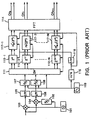
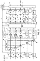
- FIG. 1 of the accompanying drawings shows the transmultiplexer disclosed in the above JP, A, 63-200635 document.
- the transmultiplexer comprises a local oscillator 101 for generating a local oscillation signal to convert an intermediate-frequency signal to a baseband signal, a multiplex clock generator 109 for generating a multiplex clock having a frequency of N ⁇ f, a divide-by-N/m frequency divider 115 for frequency-dividing the multiplex clock by N/m, and a divide-by-m frequency divider 116 for frequency-dividing an interpolation clock by m.
- a mixer 103 is supplied with the intermediate-frequency signal and the local oscillation signal, and another mixer 104 is supplied with the intermediate-frequency signal and the local oscillation signal which has been delayed in phase by ⁇ /2 by a ⁇ /2 phase shifter 102.
- the mixers 103, 104 have respective output terminals connected respectively through low-pass filters (LPFs) 105, 106 to respective analog-to-digital (A/D) converters 107, 108.
- LPFs low-pass filters
- the transmultiplexer also includes a switching circuit 111 for carrying out signal branching and sampling.
- the switching circuit 111 is supplied with output signals from the A/D converters 107, 108 and separates the inputted time sequence of signals into N separate output signals in every N samples.
- the N output signals from the switching circuit 111 are supplied through respective delay units 112-1 ⁇ 112-N to respective interpolating digital subfilters 117-1 ⁇ 117-N.
- the delay units 112-1 ⁇ 112-N serve to delay the supplied signals by time lags proportional to the order in which the signals come in, for thereby generating timed baseband signals.
- the transmultiplexer further has a fast Fourier transform (FFT) circuit 114 for effecting a complex fast Fourier transform of N points on respective output signals from the interpolating digital subfilters 117-1 ⁇ 117-N.
- the FFT circuit 114 produces N complex output signals as respective channel output signals of the transmultiplexer.
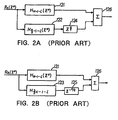
- FIG. 2A shows an arrangement of an interpolating digital subfilter 117-i where (N/2) + 1 ⁇ i ⁇ N
- FIG. 2B of the accompanying drawings shows an arrangement of an interpolating digital subfilter 117-i where 1 ⁇ i ⁇ N/2
- the interpolating digital subfilter comprises two digital subfilters 121, 122 connected to an input terminal, a delay circuit 124 for delaying an output signal from the digital subfilter 122, and an adder 126 for adding output signals from the digital subfilter 121 and the delay circuit 124.
- the interpolating digital subfilter comprises two digital subfilters 121, 122 connected to an input terminal, a delay circuit 124 for delaying an output signal from the digital subfilter 122, and an adder 126 for adding output signals from the digital subfilter 121 and the delay circuit 124.
- the interpolating digital subfilter comprises two digital subfilters 121, 123 connected to an input terminal, a delay circuit 125 for delaying an output signal from the digital subfilter 123, and an adder 126 for adding output signals from the digital subfilter 121 and the delay circuit 125.
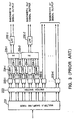
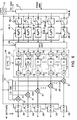
- FIG. 3 illustrates the revealed variable-bandwidth FDM signal branching circuit.
- the variable-bandwidth FDM signal branching circuit has a switch matrix 222 connected to output terminals of a multiple-sampling transmultiplexer (TMUX) 221 having a structure shown in FIG. 1, and k signal interpolation circuits 223-1 ⁇ 223-k connected to output terminals of the switch matrix 222.
- TMUX multiple-sampling transmultiplexer
- variable-bandwidth FDM signal branching circuit outputs (k-5) signals each having a bandwidth of ⁇ f, a signal having a bandwidth of 2 ⁇ f, and a signal having a bandwidth of 3 ⁇ f.
- the (k-5) signals each having a bandwidth of ⁇ f are outputted respectively from the signal interpolation circuits 223-6 ⁇ 223-k.
- the signal having a bandwidth of 2 ⁇ f is produced when output signals from the signal interpolation circuits 223-1, 223-2 are transferred through respective frequency shifters 224-1, 224-2 and added to each other by an adder 225-1, and a sum signal from the adder 225-1 is passed through an analog low-pass filter 226-1.
- the signal having a bandwidth of 3 ⁇ f is produced when output signals from the signal interpolation circuits 223-3 ⁇ 223-5 are transferred through respective frequency shifters 224-3 ⁇ 224-5 and added to each other by an adder 225-2, and a sum signal from the adder 225-2 is passed through an analog low-pass filter 226-2.
- the conventional multiple-sampling-type transmultiplexer Since the sampling frequency is 2 ⁇ f and the bandwidth of a signal for each channel is restricted to ⁇ f, the conventional multiple-sampling-type transmultiplexer needs a wide bandwidth for multiplexing channels, and hence requires a signal conversion to a signal sequence with an increased sampling frequency, i.e., an interpolation process. Accordingly, the conventional multiple-sampling-type transmultiplexer necessarily becomes large in circuit scale because of the need for interpolation circuits.
- a channel multiplexer which employs the above conventional multiple-sampling-type transmultiplexer is also large in circuit scale as it has signal interpolation circuits and frequency shifters.
- the channel multiplexer requires N ⁇ N full matrix switch elements in order to increase the bandwidth of a channel in any arbitrary frequency position. As a result, the channel multiplexer still remains large in circuit scale.
- variable-bandwidth frequency-division multiplex communication system having a transmission device including a signal combining circuit and a reception device including a signal branching circuit, for establishing channels having a frequency band wider than a channel frequency interval ⁇ f.
- the signal combining circuit has a sampling timing generator for generating a sampling frequency f s which is a multiple by a natural number of the channel frequency interval ⁇ f, a plurality of A/D converters associated respectively with N independent information signals to be transmitted, N being a natural number, for sampling the corresponding information signals at the sampling frequency f s and converting the information signals to digital signals, a complex local oscillator for generating complex signals each having a frequency which is k times the channel frequency interval ⁇ f, k being an integer ranging from 0 to N-1, N complex multipliers for multiplying the digital signals from the A/D converters by the respective complex signals from the complex local oscillator, and producing N output signals, an inverse Fourier transform circuit for effecting a complex inverse Fourier transform of N points, an N-input/N-output switch circuit connected between output terminals of the complex multipliers and input terminals of the inverse Fourier transform circuit, a plurality of digital subfilters connected respectively to N output terminals of the inverse Fourier transform
- the signal branching circuit has a sampling timing generator for generating a sampling frequency f s which is a multiple by a natural number of the channel frequency interval ⁇ f, an N-output shift register for shifting a complex digital numerical sequence of a received digital signal in synchronism with the sampling frequency f s , N being a natural number, a sampling circuit for sampling output signals from respective stages of the shift register in synchronism with the sampling frequency f s , a plurality of digital subfilters for filtering respective N signals outputted parallel from the sampling circuit, a Fourier transform circuit for effecting a complex Fourier transform of N points on respective output signals from the digital subfilters, an N-input/N-output switch circuit connected to output terminals of the Fourier transform circuit, a complex local oscillator for generating complex signals each having a frequency which is k times the channel frequency interval ⁇ f, k being an integer ranging from 0 to N-1, N complex multipliers for multiplying output signals from the switch circuit by the respective complex signals from the
- the objects of the present invention can also be achieved by a variable-bandwidth frequency-division multiplex communication system for achieving a multiplex access using a relay station having antennas corresponding to respective geographic regions, to provide a complete connection between the regions.
- the relay station has as many sets of a reception device and a transmission device as the number of the antennas, and a baseband switch matrix.
- Signal branching circuits, each identical to the above signal branching circuit, are connected between the reception devices and the baseband switch matrix, and signal combining circuits, each identical to the above signal combining circuit, are connected between the transmission devices and the baseband switch matrix.
- the sampling timing generator and the complex local oscillator may be shared by the signal branching circuits and the signal combining circuits.
- variable-bandwidth communication network having a flat frequency characteristic curve from a narrow-bandwidth communication network having a step frequency (channel frequency interval) of ⁇ f, the variable-bandwidth communication network having a bandwidth which is an integral multiple of the bandwidth of the narrow-bandwidth communication network. Because a filter bank is realized by a digital signal processing technology, the variable-bandwidth frequency-division multiplex communication system provide highly accurate characteristics, but is small in size, lightweight, has a low power requirement, and is highly reliable in operation.
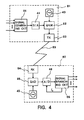
- a variable-bandwidth frequency-division multiplex communication system generally comprises a transmission device 81 and a reception device 82 which are connected to each other by a circuit 83.
- the transmission device 81 comprises a variable-bandwidth transmission device
- the reception device 82 comprises a variable-bandwidth reception device.
- the transmission device 81 comprises a signal combining circuit 91 for combining N independent information signals, N being a natural number, with a transmultiplexer according to the present invention, a high-speed digital-to-analog (D/A) converter 44 for converting a digital output signal from the signal combining circuit 91 to an analog signal, a local oscillator 40 for outputting a carrier, a quadrature amplitude modulation (QAM) circuit 92 for quadrature-amplitude-modulating the carrier from the local oscillator 40 with an output signal from the high-speed D/A converter 44, and a transmitter 93 for transmitting a modulated output signal from the QAM circuit 92 through the circuit 83 to the reception device 82.
- D/A digital-to-analog
- QAM quadrature amplitude modulation
- the reception device 82 comprises a receiver 94 for receiving a signal transmitted through the circuit 83 from the transmission device 81 as a received intermediate-frequency (IF) signal, a local oscillator 45 for generating a local oscillation signal having substantially the same frequency as the carrier outputted from the local oscillator 40 in the transmission device 81, a quadrature amplitude demodulation (QAD) circuit 95 for quadrature-amplitude-demodulating the received IF signal with the local oscillation signal, an A/D converter 48 for sampling a demodulated output signal from the QAD circuit 95 with a sampling frequency f s and converting it to a digital signal, and a signal branching circuit 96 for supplying a signal of the sampling frequency f s to the A/D converter 48 and branching the digital signal outputted from the A/D converter 48 into N information signals with the transmultiplexer according to the present invention.
- IF intermediate-frequency
- the sampling frequency f s is generated independently in the transmission device 81 and the reception device 82.
- the signal combining circuit 91 in the transmission device 81 will be described below with reference to FIG. 5.
- the signal combining circuit 91 includes a sampling timing generator 1 for generating a signal of the sampling frequency f s and N A/D converters 3 for sampling N independent information signals with the sampling frequency f s and converting them to digital signals.
- the term "complex" contained in the complex local signal signifies the simultaneous generation of cosine and sine components.
- the term "N-output" contained in the N-output complex local oscillator 4 means the simultaneous outputting of N sets of signals.
- the A/D converters 3 have respective output terminals connected to respective complex multipliers 5.
- an i-th (1 ⁇ i ⁇ N) information signal to be transmitted is supplied to and converted by an i-th A/D converter 3 to a digital signal, which is multiplied by a complex local signal having a frequency of (i-1) ⁇ f in an i-th complex multiplier 5.
- Output signals from the complex multipliers 5 are supplied to a switch circuit (i.e., switch matrix 6) which is controlled by a controller 8.
- the switch matrix 6 comprises N 3-input/1-output switch elements 7 each having input terminals S 1 , S 2 , S 3 .
- the output signal from an i-th (1 ⁇ i ⁇ N) complex multiplier 5 is supplied to the input terminal S 2 of an i-th switch element 7 and the input terminal S 1 of an (i+1)th switch element 7.
- the input terminal S 3 of an i-th switch element 7 is connected to the output terminal of an (i+1)th switch element 7. If i + 1 > N , however, then no such connection is made for an i-th switch element 7.
- the input terminals S 1 , S 2 , S 3 of the switch elements 7 are individually switched one from another by the controller 8.
- the signal combining circuit 91 also has an inverse fast Fourier transform (IFFT) circuit 9 for effecting an inverse fast Fourier transform of N-points on output signals from the switch elements 7 which are supplied as input signals to the IFFT circuit 9.
- the IFFT circuit 9 is also supplied with the sampling frequency f s .
- the IFFT circuit 9 produces N complex output signals which are supplied through respective digital subfilters 10-1 ⁇ 10-N to respective delay units 11-1 ⁇ 11-N.
- the digital filters 10-1 ⁇ 10-N and the delay units 11-1 ⁇ 11-N are supplied with the sampling frequency f s .
- An i-th digital subfilter 10-i serves to effect a filtering process whose transfer characteristic is expressed by G i-1 (Z N ).
- the N digital subfilters 10-1 ⁇ 10-N jointly make up a digital filter circuit.
- An i-th delay unit 11-i serves to give a time lag expressed by (i-1)/ ⁇ f .
- the N delay units 11-1 ⁇ 11-N jointly make up a delay circuit.
- Complex output signals from the delay units 11-1 ⁇ 11-N are added together by an adder 12, which supplies a sum signal as a complex sample sequence of data to the high-speed D/A converter 44 (see FIG. 4).
- the high-speed D/A converter 44 converts the supplied complex sample sequence to a complex continuous signal, which is applied to QAM circuit 92 (see FIG. 4).
- the signal branching circuit 96 in the reception device 82 will be described below with reference to FIG. 6.
- the signal branching circuit 96 includes a sampling timing generator 13 for generating a signal having substantially the same frequency as the sampling timing generator 1 in the signal combining circuit 91. Since the frequencies generated by the sampling timing generators 1, 13 are substantially the same as each other, the frequency generated by the sampling timing generator 13 in the signal branching circuit 96 is also referred to as a sampling frequency f s .
- a complex output signal from the QAD circuit 95 (see FIG. 4) is sampled and converted by the A/D converter 48 (see FIG. 4) with the sampling frequency f s to a digital signal.
- the digital signal is supplied as a complex digital numerical sequence of data to a shift register 27.
- the shift register 27 comprises a 1-input/N-output shift register that is driven by the sampling frequency f s .
- the shift register 27 produces complex output signals which are outputted from respective stages of the shift register 27 and supplied to respective sampling circuits 26-1 ⁇ 26-N.
- the sampling circuit 26-1 ⁇ 26-N sample the supplied complex output signals based on the sampling frequency f s .
- Sampled signals from the sampling circuits 26-1 ⁇ 26-N are then supplied to respective digital sub-filters 25-1 ⁇ 25-N.
- An i-th digital subfilter 15-i serves to perform a filtering process whose fundamental filter characteristic is expressed by H i-1 (Z N ).
- the N digital subfilters 25-1 ⁇ 25-N jointly make up a digital filter circuit.
- the signal branching circuit 96 also has a fast complex Fourier transform (FFT) circuit 24 for effecting a fast complex Fourier transform of N points on N parallel output signals (a complex numerical sequence of data) from the respective digital subfilters 25-1 ⁇ 25-N.
- the FFT circuit 24 has output terminals connected to a switch circuit 22 which is controlled by a controller 19.
- the switch circuit 22 comprises N first adders 16 coupled respectively to the output terminals of the FFT circuit 24, N 1-input/3-output switch elements 17 for being supplied with respective output signals from the adders 16, and N second adders 18 coupled respectively to output terminals of the switch elements 17.
- Each of the switch elements 17 has output terminals T 1 , T 2 , T 3 .
- An i-th first adder 16 adds a complex output signal from an i-th output terminal of the FFT circuit 24 and an output signal from the output terminal T 3 of an (i-1)th switch element 17, and outputs a sum signal to an i-th switch element 17.
- An i-th second adder 18 adds an output signal from the output terminal T 2 of an i-th switch element 17 and an output signal from the output terminal T 1 of an (i+1)th switch element 17, and outputs a sum signal. If i+1 > N or i-1 ⁇ 0, then no such connection is made for an i-th first adder 16, an i-th switch element 17, and i-th second adder 18.
- the output terminals T 1 , T 2 , T 3 of the switch elements 17 are individually switched one from another by the controller 19.
- the second adders 18 have respective output terminals connected to respective complex multipliers 21.
- the complex multipliers 21 have respective output terminals connected respectively to N D/A converters 20 which convert output signals from the complex multipliers 21 to analog signals based on the sampling frequency f s .
- a complex output signal from an i-th second adder 18 is multiplied by a complex local signal having a frequency of (i-1) ⁇ f in an i-th complex multiplier 21, which supplies an output signal to an i-th D/A converter 20 that converts the supplied signal to an analog signal as an output signal (i.e., information signal).
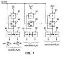
- Each of the complex local oscillators 4, 14 is shown in detail in FIG. 7.
- Each of the complex local oscillators 4, 14 comprises a plurality of blocks for generating respective complex local signals having respective frequencies to be outputted by each of the complex local oscillators 4, 14.
- Each of the blocks is constructed as a direct digital synthesizer (DDD), and has a D flip-flop 30, a table circuit 31 for generating a cosine component waveform, another table circuit 32 for generating a sine component waveform, and an adder 33.
- the D flip-flop 30 has a clock (C) terminal supplied with a common clock having the sampling frequency f s , for example.
- the adder 33 in that block is supplied with a numerical value corresponding to k ⁇ f/f s and an output signal from a terminal Q of the D flip-flop 30 in the same block, and outputs a sum signal to a terminal D of the D flip-flop 30.
- the terminal Q of the D flip-flop 30 is connected to respective input terminals of the table circuits 31, 32.
- the table circuits 31, 32 are in the form of lookup tables, respectively, and comprise respective read-only memories (ROMs), for example.
- ROMs read-only memories
- each of the complex local oscillators 4, 14 generate complex local signals having respective frequencies of 0, ⁇ f, 2 ⁇ f, ⁇ , (N-1) ⁇ f. Since complex frequencies are considered here, a frequency (N-1) ⁇ f is equivalent to a frequency - ⁇ f.
- FIG. 8A shows the QAM circuit 92 in detail
- FIG. 8B shows the QAD circuit 95 in detail.
- the signal combining circuit 91 outputs a complex digital signal, and a complex digital signal is inputted to the signal branching circuit 96.
- a complex digital signal outputted from the signal combining circuit 91 is converted by two high-speed D/A converters 44 to two analog signals corresponding respectively to real and imaginary components, which are supplied to the QAM circuit 92.
- the two high-speed D/A converters 44 are shown in FIG. 8A because they convert the real and imaginary components, respectively, of the supplied complex digital signal.
- the QAM circuit 92 comprises a ⁇ /2 phase shifter 41 for shifting the phase of the local oscillation signal (i.e., carrier) from the local oscillator 40 by ⁇ /2 (90 degrees), and outputting the phase-shifted local oscillation signal, two mixers 42 for being supplied with the two analog signals from the respective D/A converters 44, and a combiner 43 for combining output signals from the respective mixers 42.
- One of the mixers 42 is supplied with the local oscillation signal directly from the local oscillator 40, and the other mixers 42 is supplied with the phase-shifted local oscillation signal from the ⁇ /2 phase shifter 41.
- the QAD circuit 95 comprises a ⁇ /2 phase shifter 46 for shifting the phase of the local oscillation signal from the local oscillator 45 by ⁇ /2, and outputting the phase-shifted local oscillation signal, and two mixers 47 for being supplied with the received IF signal from the receiver 94 (see FIG. 4).
- One of the mixers 47 is supplied with the local oscillation signal directly from the local oscillator 45, and the other mixers 47 is supplied with the phase-shifted local oscillation signal from the ⁇ /2 phase shifter 46.
- Output signals from the respective mixers 47 are sampled and converted by two A/D converters 48 to digital signals, which are supplied as a complex digital signal to the signal branching circuit 96.
- the two A/D converters 48 are shown in FIG. 8B because they correspond to real and imaginary components, respectively, and output real and imaginary number components of the complex digital signal, respectively.
- variable-bandwidth frequency-division multiplex communication system of the present embodiment Operation of the variable-bandwidth frequency-division multiplex communication system of the present embodiment will be described below. First, a signal processing procedure in the transmission device 81 will first be described below.
- the signal in each channel is passed through the channel filter G(Z) and shifted to a designated frequency position, and thereafter the signals in all channels are added together, then there is obtained a frequency-division multiplex signal to be transmitted.
- a variable conversion represented by: Z ⁇ exp(-j ⁇ k /f s )*Z may be carried out.
- Such a signal combining process is carried out by the signal combining circuit 91 shown in FIG. 5.
- An input signal sequence which has been converted into a digital value by the A/D converters 3 is frequency-converted by the complex local oscillator 4 and the complex multipliers 5.
- This frequency conversion corresponds to a conversion in the equation (13), expressed by: x k (Z) ⁇ x k (exp(-j2 ⁇ k /N)*Z)
- the input signal sequence thus frequency-converted is inverse-complex-Fourier-transformed by the IFFT circuit 9, filtered by the digital subfilters 10-1 ⁇ 10-N, and passed through the delay units 11-1 ⁇ 11-N, whose output signals are added altogether by the adder 12. It can clearly be seen that these processing steps correspond to the right side of the equation (13).
- the output signal Y(Z) thus produced which is to be transmitted comprises a complex digital signal, and is converted into an analog signal by the high-speed D/A con-verter 44. Thereafter, the signal is converted by the QAM circuit 92 to a quadrature-amplitude-modulated signal, which is transmitted from the transmitter 93 to the reception device 82.
- a signal processing procedure in the reception device 82 will be described below.
- the signal received by the receiver 94 is supplied as a received IF signal to the QAD circuit 95, which demodulates the signal.
- the demodulated signal is converted by the A/D converter 48 to a complex digital signal that is applied to the signal branching circuit 96.
- the frequency conversion (frequency shift) is expressed by: Z ⁇ Z*exp(j2 ⁇ k/N)
- H(Z) a selected output signal of the k-th channel is obtained.
- Such a frequency branching process is carried out by the signal branching circuit 96.
- the complex digital signal that is applied from the A/D converter 48 to the signal branching circuit 96 is divided by the shift register 27 and the sampling circuits 26-1 ⁇ 26-N into N complex digital signals which are filtered by the digital subfilters 25-1 ⁇ 25-N.
- the filtered signals are then applied to the FFT circuit 24, which effects a fast complex Fourier transform thereon.
- the circuits ranging from the shift register 27 to the output terminals of the FFT circuit 24 serve as a filter bank.
- a k-th output signal from the FFT circuit 24 has a central frequency of ⁇ k and exhibits bandpass filter characteristics expressed by the fundamental filter H(Z).
- the switch circuit 22 When output signals of adjacent channels from the FFT circuit 24 are added together by the switch circuit 22, it is possible to provide filter banks of various frequency characteristics.
- the switch circuit 6 in the transmission device 81 it is possible for the switch circuit 6 in the transmission device 81 to distribute signals in frequency bands wider than the channel interval ⁇ f to a plurality of adjacent channels through the operation of the switch elements 7. Consequently, the variable-bandwidth frequency-division multiplex communication system according to the present invention can transmit signals in frequency bands wider than the channel interval ⁇ f.
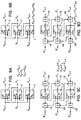
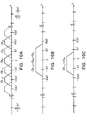
- FIGS. 9A, 9B, 9C, and 9D schematically illustrate how the switch elements 7, 17 in the switch circuits 6, 22 operate.
- each of the switch elements 7 comprises a 3-input/1-output switch element
- each of the switch elements 17 comprises a 1-input/3-output switch element.
- switch elements 17 select signals supplied to the respective output terminals S2, they supply the input signals as they are from the FFT circuit 24.
- the three adjacent switch elements 17 are controlled as shown in FIG. 9D, one of them adds the signals in the three adjacent channels and outputs a sum signal to a corresponding output terminal of the switch circuit 22.
- the switch arrangements shown in FIGS. 9B and 9D are combined with each other, they can transmit a signal with a bandwidth corresponding to three channels.
- FIGS. 10A, 10B, and 10C show the principles by which a frequency band spreads beyond the frequency interval ⁇ f according to the present embodiment.
- the fundamental filter H(Z) for each channel has such characteristics that when filters whose central frequencies deviate by ⁇ f are combined, the total frequency characteristic curve is flat as shown in FIG. 10A.
- the digital subfilters 10-1 ⁇ 10-N in the signal combining circuit 91 or the digital subfilters 25-1 ⁇ 25-N in the signal branching circuit 96 serve as one digital filter as a whole, and their frequency characteristic curve becomes completely flat in frequency regions [0, ⁇ f] when folded and superposed at a frequency of ⁇ f/2.
- Filters of such frequency characteristics are filters of Nyquist frequency characteristics having a Nyquist frequency of ⁇ f/2, and are widely used in communication networks. With fundamental filters of such frequency characteristics being established, when adjacent m channels are combined together, it is possible to construct a variable filter bank whose bandwidth is m times the bandwidth of each filter and whose transmission characteristic curve is flat. For example, when three successive channels (Ch 1 , Ch 0 , Ch -1 ) shown in FIG. 10B are combined together, a bandwidth for three channels can be obtained, and when two successive channels (Ch 0 , Ch -1 ) shown in FIG. 10C are combined together, a bandwidth for two channels can be obtained.
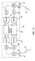
- a satellite-switched frequency-division multiple access system which is a typical example that incorporates the variable-bandwidth frequency-division multiplex communication system shown in FIG. 4, will be described below with reference to FIG. 11.
- the satellite-switched frequency-division multiple access system includes a relay station 50 on a communication satellite which has an antenna 51 corresponding to a first beam 64 and an antenna 52 corresponding to a second beam 65.
- a relay station 50 on a communication satellite which has an antenna 51 corresponding to a first beam 64 and an antenna 52 corresponding to a second beam 65.
- An arrangement for achieving a complete connection between channels using a baseband switch matrix 53 between the two beams 64, 65 will be described below.
- the first and second beams 64, 65 correspond to different geographic regions in a service area covered by the communication satellite.
- the antennas 51, 52 are connected respectively to signal branching units (DPX) 54, 55 for sharing transmission and reception waves.
- the signal branching circuit 54 is connected to a transmission device (TX) 56 and a reception device (RX) 58, and the signal branching circuit 55 is connected to a transmission device (TX) 57 and a reception device (RX) 59.
- Signal combining circuits (TMUX) 60, 61 are connected between the transmission devices 56, 57 and the baseband switch matrix 53.
- signal branching circuits (TDUX) 62, 63 each identical to the signal branching circuit shown in FIG.
- the reception devices 58, 59 and the baseband switch matrix 53 are connected between the reception devices 58, 59 and the baseband switch matrix 53. Since the signal combining circuits 60, 61 and the signal branching circuits 62, 63 are disposed in the same relay station 50, the sampling timing generator and the complex local oscillator may be shared by the signal combining circuits 60, 61 and the signal branching circuits 62, 63. Because the baseband switch matrix 53 usually comprises a digital signal processor, D/A converters on the input side of the signal combining circuits 60, 61 and A/D converters on the output side of the signal branching circuits 62, 63 are unnecessary.
- the relay station 50 of the above arrangement can achieve a multiple access capable of a complete connection in a variable bandwidth between channels between the first and second beams 64, 65 through the baseband switch matrix 53.
Abstract
Description
- The present invention relates to a frequency-division multiplex (FDM) technology widely used in the art of communications and measurements, and more particularly to a variable-bandwidth frequency-division multiplex communication system capable of dividing and multiplexing frequency channels with the frequency band of each frequency channel being variable.
- Transmultiplexers (TMUX) are equipment for efficiently branching and combining a number of frequency-division multiplex signals according to batch digital signal processing. The transmultiplexers are widely used in the field of communications for mutual transformation between frequency-division multiplex signals and time-division multiplex (TDM) signals. The fundamental concept of transmultiplexers is proposed in Maurice G. Bellanger and Jacques L. Daguet, "TDM-FDM Transmultiplexer: Digital Polyphase and FFT", IEEE Trans., COM-22, No. 9, September 1974.
- Conventional transmultiplexers suffer a problem in that if the frequency interval between FDM channels is expressed by Δf, then the maximum bandwidth of each FDM channel is limited to Δf. Multimedia communications which are currently drawing much attention require flexible communication paths which are capable of communications in a variety of bandwidths. The conventional transmultiplexers are not suitable for multimedia communications because of the fixed frequency band for each channel. Consequently, research efforts have been directed to transmultiplexers which are able to perform communications in variable bandwidths.
- For example, Japanese laid-open patent publication No. 63-200635 (JP, A, 63-200635) discloses a transmultiplexer of the multiple sampling type. The multiple-sampling-type transmultiplexer uses an interpolating digital subfilter, and generates a channel clock and an interpolation clock whose frequency is m times the frequency of the channel clock. The interpolating digital subfilter carries out a predetermined filtering process based on the timing provided by the channel clock and the interpolation clock, and generates a filter output at the sampling rate of the interpolation clock. The filter output is supplied to a Fourier transform circuit.
- FIG. 1 of the accompanying drawings shows the transmultiplexer disclosed in the above JP, A, 63-200635 document. In the transmultiplexer, it is assumed that an intermediate-frequency (IF) signal is supplied as an input thereto, a channel interval is represented by Δf, and the multiplex level by N. The transmultiplexer comprises a
local oscillator 101 for generating a local oscillation signal to convert an intermediate-frequency signal to a baseband signal, amultiplex clock generator 109 for generating a multiplex clock having a frequency of NΔf, a divide-by-N/m frequency divider 115 for frequency-dividing the multiplex clock by N/m, and a divide-by-m frequency divider 116 for frequency-dividing an interpolation clock by m. Amixer 103 is supplied with the intermediate-frequency signal and the local oscillation signal, and anothermixer 104 is supplied with the intermediate-frequency signal and the local oscillation signal which has been delayed in phase by π/2 by a π/2phase shifter 102. Themixers converters - The transmultiplexer also includes a
switching circuit 111 for carrying out signal branching and sampling. Specifically, theswitching circuit 111 is supplied with output signals from the A/D converters switching circuit 111 are supplied through respective delay units 112-1 ∼ 112-N to respective interpolating digital subfilters 117-1 ∼ 117-N. The delay units 112-1 ∼ 112-N serve to delay the supplied signals by time lags proportional to the order in which the signals come in, for thereby generating timed baseband signals. The transmultiplexer further has a fast Fourier transform (FFT)circuit 114 for effecting a complex fast Fourier transform of N points on respective output signals from the interpolating digital subfilters 117-1 ∼ 117-N. TheFFT circuit 114 produces N complex output signals as respective channel output signals of the transmultiplexer. - FIG. 2A shows an arrangement of an interpolating digital subfilter 117-i where


digital subfilters delay circuit 124 for delaying an output signal from thedigital subfilter 122, and anadder 126 for adding output signals from thedigital subfilter 121 and thedelay circuit 124. According to the arrangement shown in FIG. 2B, the interpolating digital subfilter comprises twodigital subfilters delay circuit 125 for delaying an output signal from thedigital subfilter 123, and anadder 126 for adding output signals from thedigital subfilter 121 and thedelay circuit 125. - Another document JP, A, 63-200636 reveals a variable-bandwidth FDM signal branching circuit which employs the above multiple-sampling-type transmultiplexer. FIG. 3 illustrates the revealed variable-bandwidth FDM signal branching circuit. As shown in FIG. 3, the variable-bandwidth FDM signal branching circuit has a
switch matrix 222 connected to output terminals of a multiple-sampling transmultiplexer (TMUX) 221 having a structure shown in FIG. 1, and k signal interpolation circuits 223-1 ∼ 223-k connected to output terminals of theswitch matrix 222. It is assumed that the variable-bandwidth FDM signal branching circuit outputs (k-5) signals each having a bandwidth of Δf, a signal having a bandwidth of 2Δf, and a signal having a bandwidth of 3Δf. The (k-5) signals each having a bandwidth of Δf are outputted respectively from the signal interpolation circuits 223-6 ∼ 223-k. The signal having a bandwidth of 2Δf is produced when output signals from the signal interpolation circuits 223-1, 223-2 are transferred through respective frequency shifters 224-1, 224-2 and added to each other by an adder 225-1, and a sum signal from the adder 225-1 is passed through an analog low-pass filter 226-1. The signal having a bandwidth of 3Δf is produced when output signals from the signal interpolation circuits 223-3 ∼ 223-5 are transferred through respective frequency shifters 224-3 ∼ 224-5 and added to each other by an adder 225-2, and a sum signal from the adder 225-2 is passed through an analog low-pass filter 226-2. - Since the sampling frequency is 2Δf and the bandwidth of a signal for each channel is restricted to Δf, the conventional multiple-sampling-type transmultiplexer needs a wide bandwidth for multiplexing channels, and hence requires a signal conversion to a signal sequence with an increased sampling frequency, i.e., an interpolation process. Accordingly, the conventional multiple-sampling-type transmultiplexer necessarily becomes large in circuit scale because of the need for interpolation circuits. A channel multiplexer which employs the above conventional multiple-sampling-type transmultiplexer is also large in circuit scale as it has signal interpolation circuits and frequency shifters. If only some of the channels are associated with frequency shifters so as to reduce the circuit scale, then the channel multiplexer requires N × N full matrix switch elements in order to increase the bandwidth of a channel in any arbitrary frequency position. As a result, the channel multiplexer still remains large in circuit scale.
- It is an object of the present invention to provide a variable-bandwidth frequency-division multiplex communication system which needs no interpolation circuits, but uses switch elements of simple structure for achieving fully bandwidth-variable communications.
- According to the present invention, the above object can be accomplished by a variable-bandwidth frequency-division multiplex communication system having a transmission device including a signal combining circuit and a reception device including a signal branching circuit, for establishing channels having a frequency band wider than a channel frequency interval Δf.
- The signal combining circuit has a sampling timing generator for generating a sampling frequency fs which is a multiple by a natural number of the channel frequency interval Δf, a plurality of A/D converters associated respectively with N independent information signals to be transmitted, N being a natural number, for sampling the corresponding information signals at the sampling frequency fs and converting the information signals to digital signals, a complex local oscillator for generating complex signals each having a frequency which is k times the channel frequency interval Δf, k being an integer ranging from 0 to N-1, N complex multipliers for multiplying the digital signals from the A/D converters by the respective complex signals from the complex local oscillator, and producing N output signals, an inverse Fourier transform circuit for effecting a complex inverse Fourier transform of N points, an N-input/N-output switch circuit connected between output terminals of the complex multipliers and input terminals of the inverse Fourier transform circuit, a plurality of digital subfilters connected respectively to N output terminals of the inverse Fourier transform circuit, for filtering output signals from the inverse Fourier transform circuit, a plurality of delay units connected respectively to output terminals of the digital subfilters, and an adder for adding output signals from the delay units and outputting a sum signal. In the signal branching circuit, a k-th delay unit (1 ≤ k ≤ N) applies a time lag expressed by

- The signal branching circuit has a sampling timing generator for generating a sampling frequency fs which is a multiple by a natural number of the channel frequency interval Δf, an N-output shift register for shifting a complex digital numerical sequence of a received digital signal in synchronism with the sampling frequency fs, N being a natural number, a sampling circuit for sampling output signals from respective stages of the shift register in synchronism with the sampling frequency fs, a plurality of digital subfilters for filtering respective N signals outputted parallel from the sampling circuit, a Fourier transform circuit for effecting a complex Fourier transform of N points on respective output signals from the digital subfilters, an N-input/N-output switch circuit connected to output terminals of the Fourier transform circuit, a complex local oscillator for generating complex signals each having a frequency which is k times the channel frequency interval Δf, k being an integer ranging from 0 to N-1, N complex multipliers for multiplying output signals from the switch circuit by the respective complex signals from the complex local oscillator, and producing N output signals, and a plurality of D/A converters connected respectively to output terminals of the complex multipliers. In the signal branching circuit, a received signal which is converted to a baseband signal and converted to a digital signal is applied to the signal branching circuit, and the D/A converters produce frequency-divided multiplex output signals.
- The objects of the present invention can also be achieved by a variable-bandwidth frequency-division multiplex communication system for achieving a multiplex access using a relay station having antennas corresponding to respective geographic regions, to provide a complete connection between the regions. The relay station has as many sets of a reception device and a transmission device as the number of the antennas, and a baseband switch matrix. Signal branching circuits, each identical to the above signal branching circuit, are connected between the reception devices and the baseband switch matrix, and signal combining circuits, each identical to the above signal combining circuit, are connected between the transmission devices and the baseband switch matrix. The sampling timing generator and the complex local oscillator may be shared by the signal branching circuits and the signal combining circuits.
- According to the present invention, it is possible to construct a variable-bandwidth communication network having a flat frequency characteristic curve from a narrow-bandwidth communication network having a step frequency (channel frequency interval) of Δf, the variable-bandwidth communication network having a bandwidth which is an integral multiple of the bandwidth of the narrow-bandwidth communication network. Because a filter bank is realized by a digital signal processing technology, the variable-bandwidth frequency-division multiplex communication system provide highly accurate characteristics, but is small in size, lightweight, has a low power requirement, and is highly reliable in operation.
- The above and other objects, features, and advantages of the present invention will become apparent from the following description with references to the accompanying drawings which illustrate an example of the present invention.
- FIG. 1 is a block diagram of a conventional multiple-sampling-type transmultiplexer;
- FIGS. 2A and 2B are block diagrams of interpolation digital subfilters for use in the conventional multiple-sampling-type transmultiplexer shown in FIG. 1;
- FIG. 3 is a block diagram of a conventional variable-bandwidth FDM signal branching circuit;
- FIG. 4 is a block diagram of a variable-bandwidth frequency-division multiplex communication system according to a preferred embodiment of the present invention;
- FIG. 5 is a block diagram of a transmultiplexer for use as a signal combining circuit in a transmission device in the variable-bandwidth frequency-division multiplex communication system shown in FIG. 4;
- FIG. 6 is a block diagram of a transmultiplexer for use as a signal branching circuit in a reception device in the variable-bandwidth frequency-division multiplex communication system shown in FIG. 4;
- FIG. 7 is a block diagram of a complex local oscillator in each of the signal combining circuit shown in FIG. 5 and the signal branching circuit shown in FIG. 6;
- FIGS. 8A and 8B are block diagrams of a quadrature amplitude modulation (QAM) circuit and a quadrature amplitude demodulation (QAD) circuit, respectively, in the variable-bandwidth frequency-division multiplex communication system shown in FIG. 4;
- FIGS. 9A and 9B are diagrams illustrative of how switch elements in the signal combining circuit operate;
- FIGS. 9C and 9D are diagrams illustrative of how switch elements in the signal branching circuit operate;
- FIGS. 10A, 10B, and 10C are diagrams showing frequency characteristics of filters in the variable-bandwidth frequency-division multiplex communication system shown in FIG. 4; and
- FIG. 11 is a block diagram of a satellite-switched frequency-division multiple access system which incorporates the variable-bandwidth frequency-division multiplex communication system shown in FIG. 4.
- As shown in FIG. 4, a variable-bandwidth frequency-division multiplex communication system according to a preferred embodiment of the present invention generally comprises a
transmission device 81 and areception device 82 which are connected to each other by acircuit 83. Thetransmission device 81 comprises a variable-bandwidth transmission device, and thereception device 82 comprises a variable-bandwidth reception device. - The
transmission device 81 comprises asignal combining circuit 91 for combining N independent information signals, N being a natural number, with a transmultiplexer according to the present invention, a high-speed digital-to-analog (D/A)converter 44 for converting a digital output signal from thesignal combining circuit 91 to an analog signal, alocal oscillator 40 for outputting a carrier, a quadrature amplitude modulation (QAM)circuit 92 for quadrature-amplitude-modulating the carrier from thelocal oscillator 40 with an output signal from the high-speed D/A converter 44, and atransmitter 93 for transmitting a modulated output signal from theQAM circuit 92 through thecircuit 83 to thereception device 82. - The
reception device 82 comprises areceiver 94 for receiving a signal transmitted through thecircuit 83 from thetransmission device 81 as a received intermediate-frequency (IF) signal, alocal oscillator 45 for generating a local oscillation signal having substantially the same frequency as the carrier outputted from thelocal oscillator 40 in thetransmission device 81, a quadrature amplitude demodulation (QAD)circuit 95 for quadrature-amplitude-demodulating the received IF signal with the local oscillation signal, an A/D converter 48 for sampling a demodulated output signal from theQAD circuit 95 with a sampling frequency fs and converting it to a digital signal, and asignal branching circuit 96 for supplying a signal of the sampling frequency fs to the A/D converter 48 and branching the digital signal outputted from the A/D converter 48 into N information signals with the transmultiplexer according to the present invention. - The sampling frequency fs is normally set to

transmission device 81 and thereception device 82. - The
signal combining circuit 91 in thetransmission device 81 will be described below with reference to FIG. 5. - As shown in FIG. 5, the
signal combining circuit 91 includes asampling timing generator 1 for generating a signal of the sampling frequency fs and N A/D converters 3 for sampling N independent information signals with the sampling frequency fs and converting them to digital signals. Thesignal combining circuit 91 also has an N-output complexlocal oscillator 4 for generating N complex local signals as digital signals having respective frequencies kΔf (
local oscillator 4 means the simultaneous outputting of N sets of signals. The A/D converters 3 have respective output terminals connected to respectivecomplex multipliers 5. Thecomplex multipliers 5 are supplied with the output digital signals from the respective A/D converters 3 and also with the complex local signals [
local oscillator 4. For example, an i-th (1 ≤ i ≤ N) information signal to be transmitted is supplied to and converted by an i-th A/D converter 3 to a digital signal, which is multiplied by a complex local signal having a frequency of (i-1)Δf in an i-thcomplex multiplier 5. Output signals from thecomplex multipliers 5 are supplied to a switch circuit (i.e., switch matrix 6) which is controlled by acontroller 8. Theswitch matrix 6 comprises N 3-input/1-output switch elements 7 each having input terminals S1, S2, S3. The output signal from an i-th (1 ≤ i ≤ N)complex multiplier 5 is supplied to the input terminal S2 of an i-th switch element 7 and the input terminal S1 of an (i+1)th switch element 7. The input terminal S3 of an i-th switch element 7 is connected to the output terminal of an (i+1)th switch element 7. If
th switch element 7. The input terminals S1, S2, S3 of theswitch elements 7 are individually switched one from another by thecontroller 8. - The
signal combining circuit 91 also has an inverse fast Fourier transform (IFFT)circuit 9 for effecting an inverse fast Fourier transform of N-points on output signals from theswitch elements 7 which are supplied as input signals to theIFFT circuit 9. TheIFFT circuit 9 is also supplied with the sampling frequency fs. TheIFFT circuit 9 produces N complex output signals which are supplied through respective digital subfilters 10-1 ∼ 10-N to respective delay units 11-1 ∼ 11-N. The digital filters 10-1 ∼ 10-N and the delay units 11-1 ∼ 11-N are supplied with the sampling frequency fs. An i-th digital subfilter 10-i serves to effect a filtering process whose transfer characteristic is expressed by Gi-1(ZN). The N digital subfilters 10-1 ∼ 10-N jointly make up a digital filter circuit. An i-th delay unit 11-i serves to give a time lag expressed by
adder 12, which supplies a sum signal as a complex sample sequence of data to the high-speed D/A converter 44 (see FIG. 4). The high-speed D/A converter 44 converts the supplied complex sample sequence to a complex continuous signal, which is applied to QAM circuit 92 (see FIG. 4). - The
signal branching circuit 96 in thereception device 82 will be described below with reference to FIG. 6. - As shown in FIG. 6, the
signal branching circuit 96 includes asampling timing generator 13 for generating a signal having substantially the same frequency as thesampling timing generator 1 in thesignal combining circuit 91. Since the frequencies generated by thesampling timing generators sampling timing generator 13 in thesignal branching circuit 96 is also referred to as a sampling frequency fs. A complex output signal from the QAD circuit 95 (see FIG. 4) is sampled and converted by the A/D converter 48 (see FIG. 4) with the sampling frequency fs to a digital signal. The digital signal is supplied as a complex digital numerical sequence of data to ashift register 27. Theshift register 27 comprises a 1-input/N-output shift register that is driven by the sampling frequency fs. Theshift register 27 produces complex output signals which are outputted from respective stages of theshift register 27 and supplied to respective sampling circuits 26-1 ∼ 26-N. The sampling circuit 26-1 ∼ 26-N sample the supplied complex output signals based on the sampling frequency fs. Sampled signals from the sampling circuits 26-1 ∼ 26-N are then supplied to respective digital sub-filters 25-1 ∼ 25-N. An i-th digital subfilter 15-i serves to perform a filtering process whose fundamental filter characteristic is expressed by Hi-1(ZN). The N digital subfilters 25-1 ∼ 25-N jointly make up a digital filter circuit. - The
signal branching circuit 96 also has a fast complex Fourier transform (FFT)circuit 24 for effecting a fast complex Fourier transform of N points on N parallel output signals (a complex numerical sequence of data) from the respective digital subfilters 25-1 ∼ 25-N.The FFT circuit 24 has output terminals connected to aswitch circuit 22 which is controlled by acontroller 19. Theswitch circuit 22 comprises Nfirst adders 16 coupled respectively to the output terminals of theFFT circuit 24, N 1-input/3-output switch elements 17 for being supplied with respective output signals from theadders 16, and Nsecond adders 18 coupled respectively to output terminals of theswitch elements 17. Each of theswitch elements 17 has output terminals T1, T2, T3. An i-thfirst adder 16 adds a complex output signal from an i-th output terminal of theFFT circuit 24 and an output signal from the output terminal T3 of an (i-1)th switch element 17, and outputs a sum signal to an i-th switch element 17. An i-thsecond adder 18 adds an output signal from the output terminal T2 of an i-th switch element 17 and an output signal from the output terminal T1 of an (i+1)th switch element 17, and outputs a sum signal. If
first adder 16, an i-th switch element 17, and i-thsecond adder 18. The output terminals T1, T2, T3 of theswitch elements 17 are individually switched one from another by thecontroller 19. - The
signal branching circuit 96 also has an N-output complexlocal oscillator 14 for generating N complex local signals having respective frequencies kΔf (
second adders 18 have respective output terminals connected to respectivecomplex multipliers 21. Thecomplex multipliers 21 are supplied with the output signals from the respectivesecond adders 18 and also with the complex local signals [
local oscillator 14. Thecomplex multipliers 21 have respective output terminals connected respectively to N D/A converters 20 which convert output signals from thecomplex multipliers 21 to analog signals based on the sampling frequency fs. For example, a complex output signal from an i-thsecond adder 18 is multiplied by a complex local signal having a frequency of (i-1)Δf in an i-th complex multiplier 21, which supplies an output signal to an i-th D/A converter 20 that converts the supplied signal to an analog signal as an output signal (i.e., information signal). - Each of the complex
local oscillators local oscillators local oscillators flop 30, atable circuit 31 for generating a cosine component waveform, anothertable circuit 32 for generating a sine component waveform, and anadder 33. The D flip-flop 30 has a clock (C) terminal supplied with a common clock having the sampling frequency fs, for example. If a complex local frequency of kΔf is to be generated by a certain block, then theadder 33 in that block is supplied with a numerical value corresponding to kΔf/fs and an output signal from a terminal Q of the D flip-flop 30 in the same block, and outputs a sum signal to a terminal D of the D flip-flop 30. The terminal Q of the D flip-flop 30 is connected to respective input terminals of thetable circuits table circuits local oscillators local oscillators - The
QAM circuit 92 and theQAD circuit 95 will be described with reference to FIGS. 8A and 8B. FIG. 8A shows theQAM circuit 92 in detail, and FIG. 8B shows theQAD circuit 95 in detail. - In the illustrated embodiment, the
signal combining circuit 91 outputs a complex digital signal, and a complex digital signal is inputted to thesignal branching circuit 96. As shown in FIG. 8A, a complex digital signal outputted from thesignal combining circuit 91 is converted by two high-speed D/A converters 44 to two analog signals corresponding respectively to real and imaginary components, which are supplied to theQAM circuit 92. The two high-speed D/A converters 44 are shown in FIG. 8A because they convert the real and imaginary components, respectively, of the supplied complex digital signal. - The
QAM circuit 92 comprises a π/2phase shifter 41 for shifting the phase of the local oscillation signal (i.e., carrier) from thelocal oscillator 40 by π/2 (90 degrees), and outputting the phase-shifted local oscillation signal, twomixers 42 for being supplied with the two analog signals from the respective D/A converters 44, and acombiner 43 for combining output signals from therespective mixers 42. One of themixers 42 is supplied with the local oscillation signal directly from thelocal oscillator 40, and theother mixers 42 is supplied with the phase-shifted local oscillation signal from the π/2phase shifter 41. - As shown in FIG. 8B, the
QAD circuit 95 comprises a π/2phase shifter 46 for shifting the phase of the local oscillation signal from thelocal oscillator 45 by π/2, and outputting the phase-shifted local oscillation signal, and twomixers 47 for being supplied with the received IF signal from the receiver 94 (see FIG. 4). One of themixers 47 is supplied with the local oscillation signal directly from thelocal oscillator 45, and theother mixers 47 is supplied with the phase-shifted local oscillation signal from the π/2phase shifter 46. Output signals from therespective mixers 47 are sampled and converted by two A/D converters 48 to digital signals, which are supplied as a complex digital signal to thesignal branching circuit 96. The two A/D converters 48 are shown in FIG. 8B because they correspond to real and imaginary components, respectively, and output real and imaginary number components of the complex digital signal, respectively. - Operation of the variable-bandwidth frequency-division multiplex communication system of the present embodiment will be described below. First, a signal processing procedure in the
transmission device 81 will first be described below. - In the
signal combining circuit 91, thesampling timing generator 1 generates sampling pulses at the sampling frequency fs, and the A/D converters 3 samples information signals in respective channels with the sampling pulses and convert them to respective digital signals. If it is assumed that an input signal (information signal) in a k-th channel to be transmitted is represented by xk(t) (
D converter 3 is expressed by:


- The characteristics of a channel filter for band-limiting the signal in each channel are expressed by:


- If the signal in each channel is passed through the channel filter G(Z) and shifted to a designated frequency position, and thereafter the signals in all channels are added together, then there is obtained a frequency-division multiplex signal to be transmitted. For example, the signal in the k-th channel is shifted to a frequency position indicated by:


- A result Yk(Z) obtained when an input signal xk(Z) in each channel is band-limited by the channel filter G(Z) is expressed by:

- To frequency-shift the result Yk(Z) to ωk, a variable conversion represented by:


- The channels each expressed by the equation (11) for


- Such a signal combining process is carried out by the
signal combining circuit 91 shown in FIG. 5. An input signal sequence which has been converted into a digital value by the A/D converters 3 is frequency-converted by the complexlocal oscillator 4 and thecomplex multipliers 5. This frequency conversion corresponds to a conversion in the equation (13), expressed by:
- The input signal sequence thus frequency-converted is inverse-complex-Fourier-transformed by the
IFFT circuit 9, filtered by the digital subfilters 10-1 ∼ 10-N, and passed through the delay units 11-1 ∼ 11-N, whose output signals are added altogether by theadder 12. It can clearly be seen that these processing steps correspond to the right side of the equation (13). - The output signal Y(Z) thus produced which is to be transmitted comprises a complex digital signal, and is converted into an analog signal by the high-speed D/A con-
verter 44. Thereafter, the signal is converted by theQAM circuit 92 to a quadrature-amplitude-modulated signal, which is transmitted from thetransmitter 93 to thereception device 82. - A signal processing procedure in the
reception device 82 will be described below. - The signal received by the
receiver 94 is supplied as a received IF signal to theQAD circuit 95, which demodulates the signal. The demodulated signal is converted by the A/D converter 48 to a complex digital signal that is applied to thesignal branching circuit 96. - It is assumed that the complex digital signal applied to the
signal branching circuit 96 is expressed by:
- A frequency branching process is to frequency-shift a signal in a channel k (


- When this result is extracted using a low-pass filter H(Z), a selected output signal of the k-th channel is obtained. The low-pass filter H(Z) is expressed by:

- An output signal to be determined is expressed by:

- Such a frequency branching process is carried out by the
signal branching circuit 96. The complex digital signal that is applied from the A/D converter 48 to thesignal branching circuit 96 is divided by theshift register 27 and the sampling circuits 26-1 ∼ 26-N into N complex digital signals which are filtered by the digital subfilters 25-1 ∼ 25-N. The filtered signals are then applied to theFFT circuit 24, which effects a fast complex Fourier transform thereon. The circuits ranging from theshift register 27 to the output terminals of theFFT circuit 24 serve as a filter bank. - A k-th output signal from the
FFT circuit 24 has a central frequency of ωk and exhibits bandpass filter characteristics expressed by the fundamental filter H(Z). When output signals of adjacent channels from theFFT circuit 24 are added together by theswitch circuit 22, it is possible to provide filter banks of various frequency characteristics. Similarly, it is possible for theswitch circuit 6 in thetransmission device 81 to distribute signals in frequency bands wider than the channel interval Δf to a plurality of adjacent channels through the operation of theswitch elements 7. Consequently, the variable-bandwidth frequency-division multiplex communication system according to the present invention can transmit signals in frequency bands wider than the channel interval Δf. - FIGS. 9A, 9B, 9C, and 9D schematically illustrate how the
switch elements switch circuits switch elements 7 comprises a 3-input/1-output switch element, whereas each of theswitch elements 17 comprises a 1-input/3-output switch element. - In the
switch circuit 6 in thetransmission device 81, as shown in FIG. 9A, when theswitch elements 7 select input signals applied to the respective input terminals S2, they supply the applied input signals as they are to theIFFT circuit 9. As shown in FIG. 9B, when the threeadjacent switch elements 7 select one input signal, the input signal is applied simultaneously to three input terminals of theIFFT circuit 9. As a result, this input signal is handled as having a bandwidth corresponding to three channels, and the bandwidth is divided into three bandwidths which are outputted from respective three digital subfilters to theadder 12. - In the
switch circuit 22 in thereception device 82, as shown in FIG. 9C, when theswitch elements 17 select signals supplied to the respective output terminals S2, they supply the input signals as they are from theFFT circuit 24. When the threeadjacent switch elements 17 are controlled as shown in FIG. 9D, one of them adds the signals in the three adjacent channels and outputs a sum signal to a corresponding output terminal of theswitch circuit 22. When the switch arrangements shown in FIGS. 9B and 9D are combined with each other, they can transmit a signal with a bandwidth corresponding to three channels. - FIGS. 10A, 10B, and 10C show the principles by which a frequency band spreads beyond the frequency interval Δf according to the present embodiment. The fundamental filter H(Z) for each channel has such characteristics that when filters whose central frequencies deviate by Δf are combined, the total frequency characteristic curve is flat as shown in FIG. 10A. Specifically, the digital subfilters 10-1 ∼ 10-N in the
signal combining circuit 91 or the digital subfilters 25-1 ∼ 25-N in thesignal branching circuit 96 serve as one digital filter as a whole, and their frequency characteristic curve becomes completely flat in frequency regions [0, Δf] when folded and superposed at a frequency of Δf/2. Filters of such frequency characteristics are filters of Nyquist frequency characteristics having a Nyquist frequency of Δf/2, and are widely used in communication networks. With fundamental filters of such frequency characteristics being established, when adjacent m channels are combined together, it is possible to construct a variable filter bank whose bandwidth is m times the bandwidth of each filter and whose transmission characteristic curve is flat. For example, when three successive channels (Ch1, Ch0, Ch-1) shown in FIG. 10B are combined together, a bandwidth for three channels can be obtained, and when two successive channels (Ch0, Ch-1) shown in FIG. 10C are combined together, a bandwidth for two channels can be obtained. - A satellite-switched frequency-division multiple access system, which is a typical example that incorporates the variable-bandwidth frequency-division multiplex communication system shown in FIG. 4, will be described below with reference to FIG. 11.
- As shown in FIG. 11, the satellite-switched frequency-division multiple access system includes a
relay station 50 on a communication satellite which has anantenna 51 corresponding to afirst beam 64 and anantenna 52 corresponding to asecond beam 65. An arrangement for achieving a complete connection between channels using abaseband switch matrix 53 between the twobeams - The first and
second beams antennas signal branching circuit 54 is connected to a transmission device (TX) 56 and a reception device (RX) 58, and thesignal branching circuit 55 is connected to a transmission device (TX) 57 and a reception device (RX) 59. Signal combining circuits (TMUX) 60, 61, each identical to the signal combining circuit shown in FIG. 5, are connected between thetransmission devices baseband switch matrix 53. Similarly, signal branching circuits (TDUX) 62, 63, each identical to the signal branching circuit shown in FIG. 6, are connected between thereception devices baseband switch matrix 53. Since thesignal combining circuits signal branching circuits same relay station 50, the sampling timing generator and the complex local oscillator may be shared by thesignal combining circuits signal branching circuits baseband switch matrix 53 usually comprises a digital signal processor, D/A converters on the input side of thesignal combining circuits signal branching circuits relay station 50 of the above arrangement can achieve a multiple access capable of a complete connection in a variable bandwidth between channels between the first andsecond beams baseband switch matrix 53. - While a preferred embodiment of the present invention has been described using specific terms, such description is for illustrative purposes only, and it is to be understood that changes and variations may be made without departing from the spirit or scope of the following claims.
Claims (14)
- A variable-bandwidth frequency-division multiplex communication system having a transmission device including a signal combining circuit and a reception device including a signal branching circuit, for establishing channels having a frequency band wider than a channel frequency interval Δf,
said signal combining circuit comprising:a sampling timing generator for generating a sampling frequency fs which is a multiple by a natural number of said channel frequency interval Δf;a plurality of A/D converters associated respectively with N independent information signals to be transmitted, N being a natural number, for sampling the corresponding information signals at said sampling frequency fs and converting the information signals to digital signals;a complex local oscillator for generating complex signals each having a frequency which is k times said channel frequency interval Δf, k being an integer ranging from 0 to N-1;N complex multipliers for multiplying the digital signals from said A/D converters by the respective complex signals from said complex local oscillator, and producing N output signals;an inverse Fourier transform circuit for effecting a complex inverse Fourier transform of N points;an N-input/N-output switch circuit connected between output terminals of said complex multipliers and input terminals of said inverse Fourier transform circuit;a plurality of digital subfilters connected respectively to N output terminals of said inverse Fourier transform circuit, for filtering output signals from said inverse Fourier transform circuit;a plurality of delay units connected respectively to output terminals of said digital subfilters; andan adder for adding output signals from said delay units and outputting a sum signal;
wherein a k-th delay unit (1 ≤ k ≤ N) applies a time lag expressed by
- The variable-bandwidth frequency-division multiplex communication system according to claim 1, wherein said sampling frequency fs is represented by NΔf, and said transmission device further comprises a high-speed D/A converter for converting a complex sample sequence outputted from said signal combining circuit to a complex continuous signal, and a quadrature amplitude modulation circuit for quadrature-amplitude-modulating a carrier with an output signal from said high-speed D/A converter.
- The variable-bandwidth frequency-division multiplex communication system according to claim 1 or 2, wherein said switch circuit comprises N 3-input/1-output switch elements each represented as a k-th switch element, and wherein said k-th switch element has:a first input terminal connected to a (k-1)th input terminal of said switch circuit;a second input terminal connected to a k-th input terminal of said switch circuit;a third input terminal connected to a (k+1)th input terminal of said switch circuit; andan output terminal connected to a k-th output terminal of said switch circuit.
- The variable-bandwidth frequency-division multiplex communication system according to claim 1, 2 or 3, wherein said complex local oscillator comprises an N-output direct digital synthesizer.
- The system according to any one of claims 1 to 4, wherein
said digital subfilters serve as a single digital filter as a whole, and have a frequency characteristic curve which becomes completely flat in frequency regions [0, Δf] when folded and superposed at a frequency of Δf/2. - The system according to any one of claims 1 to 5, wherein
said switch circuit comprises N 3-input/1-output switch elements each represented as a k-th switch element, and wherein said k-th switch element has:a first input terminal connected to a (k-1)th input terminal of said switch circuit;a second input terminal connected to a k-th input terminal of said switch circuit;a third input terminal connected to a (k+1)th input terminal of said switch circuit; andan output terminal connected to a k-th output terminal of said switch circuit. - A variable-bandwidth frequency-division multiplex communication system having a transmission device including a signal combining circuit and a reception device including a signal branching circuit, for establishing channels having a frequency band wider than a channel frequency interval Δf,
said signal branching circuit comprising:a sampling timing generator for generating a sampling frequency fs which is a multiple by a natural number of said channel frequency interval Δf;an N-output shift register for shifting a complex digital numerical sequence of a received digital signal in synchronism with said sampling frequency fs, N being a natural number;a sampling circuit for sampling output signals from respective stages of said shift register in synchronism with said sampling frequency fs;a plurality of digital subfilters for filtering respective N signals outputted parallel from said sampling circuit;a Fourier transform circuit for effecting a complex Fourier transform of N points on respective output signals from said digital subfilters;an N-input/N-output switch circuit connected to output terminals of said Fourier transform circuit;a complex local oscillator for generating complex signals each having a frequency which is k times said channel frequency interval Δf, k being an integer ranging from 0 to N-1;N complex multipliers for multiplying output signals from said switch circuit by the respective complex signals from said complex local oscillator, and producing N output signals; anda plurality of D/A converters connected respectively to output terminals of said complex multipliers. - The variable-bandwidth frequency-division multiplex communication system according to claim 7, wherein said sampling frequency fs is represented by NΔf, and said reception device further comprises a quadrature amplitude demodulation circuit for quadrature-amplitude-demodulating a received intermediate-frequency signal, and an A/D converter for sampling an output signal from said quadrature amplitude demodulation circuit at said sampling frequency fs and converting the sampled signal to a complex digital signal, which is applied to said shift register.
- The variable-bandwidth frequency-division multiplex communication system according to claim 7 or 8, wherein a received signal which is converted to a baseband signal and converted to a digital signal is applied to said signal branching circuit, and said D/A converters produce frequency-divided multiplex output signals.
- A variable-bandwidth frequency-division multiplex communication system according to claim 7, 8 or 9, wherein said switch circuit comprises N 1-input/3-output switch elements, N first adders each represented by a k-th first adder, and N second adders each represented by a k-th second adder, and wherein:said k-th second adder adds an output signal from a first output terminal of a (k+1)th switch element and an output signal from a second output terminal of a k-th switch element, and outputs a sum signal to a k-th output terminal of said switch circuit; andsaid k-th first adder adds an output signal from a third output terminal of a (k-1)th switch element and a signal from a k-th input terminal of said switch circuit, and inputs a sum signal to an input terminal of said k-th switch element.
- The system according to any one of claims 7 to 10, wherein
said complex local oscillator comprises an N-output direct digital synthesizer. - The system according to any one of claims 7 to 11, wherein
said digital subfilters serve as a single digital filter as a whole, and have a frequency characteristic curve which becomes completely flat in frequency regions [0, Δf] when folded and superposed at a frequency of Δf/2. - The system according to any one of claims 7 to 12, wherein
said switch circuit comprises N 1-input/3-output switch elements, N first adders each represented by a k-th first adder, and N second adders each represented by a k-th second adder, and wherein:said k-th second adder adds an output signal from a first output terminal of a (k+1)th switch element and an output signal from a second output terminal of a k-th switch element, and outputs a sum signal to a k-th output terminal of said switch circuit; andsaid k-th first adder adds an output signal from a third output terminal of a (k-1)th switch element and a signal from a k-th input terminal of said switch circuit, and inputs a sum signal to an input terminal of said k-th switch element. - A variable-bandwidth frequency-division multiplex communication system for achieving a multiplex access using a relay station having antennas corresponding to respective geographic regions, to provide a complete connection between said regions, said relay station having:as many sets of a reception device and a transmission device as the number of said antennas, a sampling timing generator for generating a sampling frequency fs which is a multiple by a natural number of said channel frequency interval Δf, a complex local oscillator for generating complex signals each having a frequency which is k times said channel frequency interval Δf, k being an integer ranging from 0 to N-1 and N being a natural number, a baseband switch matrix, signal branching circuits connected between the reception devices and said baseband switch matrix, and signal combining circuits connected between the transmission devices and said baseband switch matrix;each of said signal branching circuits comprising;a first complex multiplying circuit having complex multipliers associated respectively with N independent information signals outputted from said baseband switch matrix, for multiplying the information signals by the respective complex signals from said complex local oscillator and producing N output signals;an inverse Fourier transform circuit for effecting a complex inverse Fourier transform of N points;an N-input/N-output first switch circuit connected between output terminals of said first complex multiplying circuit and input terminals of said inverse Fourier transform circuit;a plurality of first digital subfilters connected respectively to N output terminals of said inverse Fourier transform circuit, for filtering output signals from said inverse Fourier transform circuit;a plurality of delay units connected respectively to output terminals of said digital subfilters; andan adder for adding output signals from said delay units and outputting a sum signal to said transmission device;
wherein a k-th delay unit (1 ≤ k ≤ N) applies a time lag expressed by each of said signal branching circuits comprising:an N-output shift register for shifting a complex digital numerical sequence from said reception device in synchronism with said sampling frequency fs;a sampling circuit for sampling output signals from respective stages of said shift register in synchronism with said sampling frequency fs;a plurality of second digital subfilters for filtering respective N signals outputted parallel from said sampling circuit;a Fourier transform circuit for effecting a complex Fourier transform of N points on respective output signals from said second digital subfilters;an N-input/N-output second switch circuit connected to output terminals of said Fourier transform circuit; anda second complex multiplying circuit having N complex multipliers for multiplying output signals from said second switch circuit by the respective complex signals, producing N output signals, and supplying the N output signals as frequency-divided multiplex signals to said baseband switch matrix.
Applications Claiming Priority (3)
| Application Number | Priority Date | Filing Date | Title |
|---|---|---|---|
| JP9283496 | 1996-04-15 | ||
| JP92834/96 | 1996-04-15 | ||
| JP9283496A JP2738385B2 (en) | 1996-04-15 | 1996-04-15 | Variable bandwidth frequency division multiplex communication system |
Publications (3)
| Publication Number | Publication Date |
|---|---|
| EP0802644A2 true EP0802644A2 (en) | 1997-10-22 |
| EP0802644A3 EP0802644A3 (en) | 2000-07-05 |
| EP0802644B1 EP0802644B1 (en) | 2004-06-30 |
Family
ID=14065468
Family Applications (1)
| Application Number | Title | Priority Date | Filing Date |
|---|---|---|---|
| EP97106084A Expired - Lifetime EP0802644B1 (en) | 1996-04-15 | 1997-04-14 | Variable-bandwith frequency division multiplex communication system |
Country Status (4)
| Country | Link |
|---|---|
| US (1) | US6014366A (en) |
| EP (1) | EP0802644B1 (en) |
| JP (1) | JP2738385B2 (en) |
| DE (1) | DE69729681T2 (en) |
Cited By (1)
| Publication number | Priority date | Publication date | Assignee | Title |
|---|---|---|---|---|
| US8687716B2 (en) | 2008-06-04 | 2014-04-01 | Sony Corporation | Digital signal transmission and reception |
Families Citing this family (31)
| Publication number | Priority date | Publication date | Assignee | Title |
|---|---|---|---|---|
| US5867479A (en) * | 1997-06-27 | 1999-02-02 | Lockheed Martin Corporation | Digital multi-channel demultiplexer/multiplex (MCD/M architecture) |
| US6442381B1 (en) * | 1998-10-30 | 2002-08-27 | Echelon Corporation | Method and apparatus for defining and generating local oscillator signals for down converter |
| JP3399400B2 (en) | 1999-04-15 | 2003-04-21 | 日本電気株式会社 | Frequency shift demodulation circuit |
| US6493358B1 (en) * | 1999-05-19 | 2002-12-10 | Ems Technologies Canada, Limited | Apparatus and method for demultiplexing a frequency division multiplexed input signal and polyphase digital filter network therefor |
| US7102692B1 (en) * | 1999-10-13 | 2006-09-05 | Thomson Licensing | Digital and analog television signal digitization and processing device |
| AU2001247819A1 (en) | 2000-03-27 | 2001-10-08 | Transcept Opencell, Inc. | Multi-protocol distributed wireless system architecture |
| US6704545B1 (en) | 2000-07-19 | 2004-03-09 | Adc Telecommunications, Inc. | Point-to-multipoint digital radio frequency transport |
| US6944406B1 (en) * | 2000-08-04 | 2005-09-13 | Fujitsu Limited | Transport system with tunable channel spacing DWDM |
| US6512799B2 (en) | 2001-02-06 | 2003-01-28 | University Of South Alabama | Digital communication system and method for increased bit rates |
| US6704372B2 (en) | 2001-09-18 | 2004-03-09 | Broadlogic Network Technologies Inc. | Digital implementation of multi-channel demodulators |
| US20030069022A1 (en) * | 2001-10-04 | 2003-04-10 | Mark Kintis | Amplitude cancellation topology for multichannel applications |
| US8811917B2 (en) | 2002-05-01 | 2014-08-19 | Dali Systems Co. Ltd. | Digital hybrid mode power amplifier system |
| US8380143B2 (en) | 2002-05-01 | 2013-02-19 | Dali Systems Co. Ltd | Power amplifier time-delay invariant predistortion methods and apparatus |
| US8958789B2 (en) | 2002-12-03 | 2015-02-17 | Adc Telecommunications, Inc. | Distributed digital antenna system |
| US7430254B1 (en) | 2003-08-06 | 2008-09-30 | Lockheed Martin Corporation | Matched detector/channelizer with adaptive threshold |
| US7424066B2 (en) * | 2005-01-21 | 2008-09-09 | Analog Devices, Inc. | Receiver structures for selectable direct conversion and low intermediate frequency operational modes |
| JP4541199B2 (en) * | 2005-03-18 | 2010-09-08 | 三菱電機株式会社 | Receiver |
| US7970345B2 (en) * | 2005-06-22 | 2011-06-28 | Atc Technologies, Llc | Systems and methods of waveform and/or information splitting for wireless transmission of information to one or more radioterminals over a plurality of transmission paths and/or system elements |
| CN102017553B (en) | 2006-12-26 | 2014-10-15 | 大力系统有限公司 | Method and system for baseband predistortion linearization in multi-channel wideband communication systems |
| JP5398242B2 (en) * | 2008-12-03 | 2014-01-29 | 株式会社東芝 | Radar signal processing device and radar device |
| CA2782338C (en) | 2009-11-30 | 2014-12-30 | Akinori Fujimura | Demultiplexing device, multiplexing device, and relay device |
| CA2791005C (en) | 2010-02-25 | 2015-09-29 | Mitsubishi Electric Corporation | Interference wave suppressing apparatus, relay apparatus, relay system, and interference wave suppressing method |
| CN107682021B (en) | 2010-08-17 | 2020-02-18 | 大力系统有限公司 | Remotely reconfigurable remote radio head unit |
| EP2611030B1 (en) | 2010-08-25 | 2019-09-25 | Mitsubishi Electric Corporation | Demultiplexing device, multiplexing device, and relay device |
| KR102136940B1 (en) | 2010-09-14 | 2020-07-23 | 달리 시스템즈 씨오. 엘티디. | Remotely Reconfigurable Distributed Antenna System and Methods |
| US9749947B2 (en) | 2013-04-19 | 2017-08-29 | Mitsubishi Electric Corporation | Wireless communication apparatus and wireless communication control method that performs communication using a frequency division multiplexing method |
| US10499269B2 (en) | 2015-11-12 | 2019-12-03 | Commscope Technologies Llc | Systems and methods for assigning controlled nodes to channel interfaces of a controller |
| CN108092704B (en) * | 2016-11-21 | 2023-04-07 | 普罗斯通信技术(苏州)有限公司 | Multi-sub-band variable bandwidth repeater |
| ES2886894T3 (en) | 2017-03-06 | 2021-12-21 | Mitsubishi Electric Corp | Demultiplexer circuit, multiplexer circuit and routing relay unit |
| WO2018208967A2 (en) * | 2017-05-11 | 2018-11-15 | Wilson Electronics, Llc | Variable channelized bandwidth booster |
| US10333639B2 (en) * | 2017-06-05 | 2019-06-25 | Capacicom Ltd. | Small-footprint digital synthesis channelizer for multiple narrowband frequency-slices |
Citations (3)
| Publication number | Priority date | Publication date | Assignee | Title |
|---|---|---|---|---|
| DE3837841C1 (en) * | 1988-10-22 | 1990-02-15 | Ant Nachrichtentechnik Gmbh, 7150 Backnang, De | Filter bank for the frequency-division multiplexing or frequency-division demultiplexing of channel signals |
| US5299192A (en) * | 1991-12-20 | 1994-03-29 | France Telecom | Digital filter-type frequency demultiplexing device |
| US5396489A (en) * | 1992-10-26 | 1995-03-07 | Motorola Inc. | Method and means for transmultiplexing signals between signal terminals and radio frequency channels |
Family Cites Families (9)
| Publication number | Priority date | Publication date | Assignee | Title |
|---|---|---|---|---|
| US3706929A (en) * | 1971-01-04 | 1972-12-19 | Philco Ford Corp | Combined modem and vocoder pipeline processor |
| FR2326818A1 (en) * | 1975-10-02 | 1977-04-29 | Thomson Csf | TELEPHONE TRANSMISSION SYSTEM, MULTIPLEXER AND DEMULTIPLEXER FOR THE IMPLEMENTATION OF SUCH A SYSTEM |
| JPS63200636A (en) * | 1987-02-17 | 1988-08-18 | Nec Corp | Variable band width fdm branching filter circuit |
| JPS63200635A (en) * | 1987-02-17 | 1988-08-18 | Nec Corp | Transmultiplexer |
| US5058107A (en) * | 1989-01-05 | 1991-10-15 | Hughes Aircraft Company | Efficient digital frequency division multiplexed signal receiver |
| US5251218A (en) * | 1989-01-05 | 1993-10-05 | Hughes Aircraft Company | Efficient digital frequency division multiplexed signal receiver |
| DE69534067T2 (en) * | 1994-05-09 | 2006-04-13 | Victor Company of Japan, Ltd., Yokohama | Setting a reference subcarrier in multi-carrier transmission |
| US5657313A (en) * | 1994-05-09 | 1997-08-12 | Victor Company Of Japan, Ltd. | Signal transmitting apparatus and signal receiving apparatus using orthogonal frequency division multiplexing |
| US5822323A (en) * | 1995-09-29 | 1998-10-13 | Victor Company Of Japan, Ltd. | Frequency division multiplexed signal generating apparatus and related decoding apparatus |
-
1996
- 1996-04-15 JP JP9283496A patent/JP2738385B2/en not_active Expired - Fee Related
-
1997
- 1997-04-14 EP EP97106084A patent/EP0802644B1/en not_active Expired - Lifetime
- 1997-04-14 DE DE69729681T patent/DE69729681T2/en not_active Expired - Fee Related
- 1997-04-15 US US08/839,753 patent/US6014366A/en not_active Expired - Fee Related
Patent Citations (3)
| Publication number | Priority date | Publication date | Assignee | Title |
|---|---|---|---|---|
| DE3837841C1 (en) * | 1988-10-22 | 1990-02-15 | Ant Nachrichtentechnik Gmbh, 7150 Backnang, De | Filter bank for the frequency-division multiplexing or frequency-division demultiplexing of channel signals |
| US5299192A (en) * | 1991-12-20 | 1994-03-29 | France Telecom | Digital filter-type frequency demultiplexing device |
| US5396489A (en) * | 1992-10-26 | 1995-03-07 | Motorola Inc. | Method and means for transmultiplexing signals between signal terminals and radio frequency channels |
Cited By (2)
| Publication number | Priority date | Publication date | Assignee | Title |
|---|---|---|---|---|
| US8687716B2 (en) | 2008-06-04 | 2014-04-01 | Sony Corporation | Digital signal transmission and reception |
| US9077598B2 (en) | 2008-06-04 | 2015-07-07 | Sony Corporation | Digital signal transmission and reception |
Also Published As
| Publication number | Publication date |
|---|---|
| US6014366A (en) | 2000-01-11 |
| JPH09284242A (en) | 1997-10-31 |
| EP0802644A3 (en) | 2000-07-05 |
| DE69729681D1 (en) | 2004-08-05 |
| DE69729681T2 (en) | 2004-12-09 |
| JP2738385B2 (en) | 1998-04-08 |
| EP0802644B1 (en) | 2004-06-30 |
Similar Documents
| Publication | Publication Date | Title |
|---|---|---|
| EP0802644B1 (en) | Variable-bandwith frequency division multiplex communication system | |
| US5299192A (en) | Digital filter-type frequency demultiplexing device | |
| KR100366751B1 (en) | Wideband FFT Channel Riser | |
| KR100338004B1 (en) | Transceiver for Multichannel Communication Networks Using Wideband FFT Channel Riser and Reverse FFT Combiner | |
| EP0534255B1 (en) | Multiple use digital transmitter/transceiver with time multiplexing | |
| KR0130471B1 (en) | Ssb signal generator | |
| US5872480A (en) | Programmable down-sampler having plural decimators and modulator using same | |
| US5519732A (en) | Digital baseband to IF conversion in cellular base stations | |
| US5889766A (en) | Transmission/reception method based on frequency division multiple access having changeable communication channel bandwidths and communication apparatus employing the method | |
| EP0613264B1 (en) | Group modulator | |
| EP1425857A2 (en) | Digital down converter | |
| US4759013A (en) | FDM-TDM transmultiplexing system | |
| JP3299952B2 (en) | Digital signal demultiplexer, digital signal multiplexer, digital signal transmitter | |
| US7130361B1 (en) | Telecommunication device with analog fourier transformation unit | |
| JP3974273B2 (en) | Communications system | |
| JP2001127736A (en) | Radio frequency transmitter of cdma type mobile communication base station system | |
| WO1997028611A1 (en) | Synchronization and downconversion in tdm/tdma systems | |
| KR20010071918A (en) | Phase domain multiplexed communications system | |
| JP3893078B2 (en) | Multichannel receiver | |
| JP6012066B2 (en) | Channelizer and signal processing method | |
| JP2754993B2 (en) | In-phase combined space diversity receiver | |
| US4001510A (en) | Digital modulator and demodulator system for fdm telephony | |
| JP2920221B2 (en) | Base station transmitter | |
| JPH0519342B2 (en) | ||
| JP2003258752A (en) | Multirate group modem, multirate group transmitter and receiver, and transmitter/receiver |
Legal Events
| Date | Code | Title | Description |
|---|---|---|---|
| PUAI | Public reference made under article 153(3) epc to a published international application that has entered the european phase |
Free format text: ORIGINAL CODE: 0009012 |
|
| AK | Designated contracting states |
Kind code of ref document: A2 Designated state(s): DE FR GB |
|
| PUAL | Search report despatched |
Free format text: ORIGINAL CODE: 0009013 |
|
| AK | Designated contracting states |
Kind code of ref document: A3 Designated state(s): DE FR GB |
|
| 17P | Request for examination filed |
Effective date: 20000529 |
|
| 17Q | First examination report despatched |
Effective date: 20030508 |
|
| GRAP | Despatch of communication of intention to grant a patent |
Free format text: ORIGINAL CODE: EPIDOSNIGR1 |
|
| GRAS | Grant fee paid |
Free format text: ORIGINAL CODE: EPIDOSNIGR3 |
|
| GRAA | (expected) grant |
Free format text: ORIGINAL CODE: 0009210 |
|
| AK | Designated contracting states |
Kind code of ref document: B1 Designated state(s): DE FR GB |
|
| REG | Reference to a national code |
Ref country code: GB Ref legal event code: FG4D |
|
| REF | Corresponds to: |
Ref document number: 69729681 Country of ref document: DE Date of ref document: 20040805 Kind code of ref document: P |
|
| ET | Fr: translation filed | ||
| PLBE | No opposition filed within time limit |
Free format text: ORIGINAL CODE: 0009261 |
|
| STAA | Information on the status of an ep patent application or granted ep patent |
Free format text: STATUS: NO OPPOSITION FILED WITHIN TIME LIMIT |
|
| 26N | No opposition filed |
Effective date: 20050331 |
|
| PGFP | Annual fee paid to national office [announced via postgrant information from national office to epo] |
Ref country code: FR Payment date: 20090417 Year of fee payment: 13 Ref country code: DE Payment date: 20090409 Year of fee payment: 13 |
|
| PGFP | Annual fee paid to national office [announced via postgrant information from national office to epo] |
Ref country code: GB Payment date: 20090408 Year of fee payment: 13 |
|
| GBPC | Gb: european patent ceased through non-payment of renewal fee |
Effective date: 20100414 |
|
| REG | Reference to a national code |
Ref country code: FR Ref legal event code: ST Effective date: 20101230 |
|
| PG25 | Lapsed in a contracting state [announced via postgrant information from national office to epo] |
Ref country code: DE Free format text: LAPSE BECAUSE OF NON-PAYMENT OF DUE FEES Effective date: 20101103 |
|
| PG25 | Lapsed in a contracting state [announced via postgrant information from national office to epo] |
Ref country code: GB Free format text: LAPSE BECAUSE OF NON-PAYMENT OF DUE FEES Effective date: 20100414 |
|
| PG25 | Lapsed in a contracting state [announced via postgrant information from national office to epo] |
Ref country code: FR Free format text: LAPSE BECAUSE OF NON-PAYMENT OF DUE FEES Effective date: 20100430 |