EP0802566A2 - Semiconductor devices, method of connecting semiconductor devices, and semicondutor device connectors - Google Patents
Semiconductor devices, method of connecting semiconductor devices, and semicondutor device connectors Download PDFInfo
- Publication number
- EP0802566A2 EP0802566A2 EP96110808A EP96110808A EP0802566A2 EP 0802566 A2 EP0802566 A2 EP 0802566A2 EP 96110808 A EP96110808 A EP 96110808A EP 96110808 A EP96110808 A EP 96110808A EP 0802566 A2 EP0802566 A2 EP 0802566A2
- Authority
- EP
- European Patent Office
- Prior art keywords
- package
- semiconductor devices
- exposed terminals
- terminals
- semiconductor
- Prior art date
- Legal status (The legal status is an assumption and is not a legal conclusion. Google has not performed a legal analysis and makes no representation as to the accuracy of the status listed.)
- Granted
Links
- 239000004065 semiconductor Substances 0.000 title claims abstract description 165
- 238000000034 method Methods 0.000 title claims abstract description 19
- 230000008878 coupling Effects 0.000 claims description 14
- 238000010168 coupling process Methods 0.000 claims description 14
- 238000005859 coupling reaction Methods 0.000 claims description 14
- 229910000679 solder Inorganic materials 0.000 claims description 11
- 238000007747 plating Methods 0.000 claims description 10
- 229910052751 metal Inorganic materials 0.000 claims description 7
- 239000000463 material Substances 0.000 claims description 6
- 239000002184 metal Substances 0.000 claims description 6
- 229920003002 synthetic resin Polymers 0.000 claims description 3
- 239000000057 synthetic resin Substances 0.000 claims description 3
- 230000000717 retained effect Effects 0.000 claims description 2
- 238000007789 sealing Methods 0.000 claims description 2
- 238000004806 packaging method and process Methods 0.000 abstract description 4
- 238000010276 construction Methods 0.000 description 9
- 239000003822 epoxy resin Substances 0.000 description 6
- 229920000647 polyepoxide Polymers 0.000 description 6
- 229920005989 resin Polymers 0.000 description 6
- 239000011347 resin Substances 0.000 description 6
- 238000009713 electroplating Methods 0.000 description 4
- 230000013011 mating Effects 0.000 description 4
- 230000003071 parasitic effect Effects 0.000 description 4
- 229910001111 Fine metal Inorganic materials 0.000 description 3
- 238000004519 manufacturing process Methods 0.000 description 2
- 230000001681 protective effect Effects 0.000 description 2
- 239000000853 adhesive Substances 0.000 description 1
- 230000001070 adhesive effect Effects 0.000 description 1
- 230000002411 adverse Effects 0.000 description 1
- 229910052782 aluminium Inorganic materials 0.000 description 1
- XAGFODPZIPBFFR-UHFFFAOYSA-N aluminium Chemical compound [Al] XAGFODPZIPBFFR-UHFFFAOYSA-N 0.000 description 1
- 239000000919 ceramic Substances 0.000 description 1
- 230000002950 deficient Effects 0.000 description 1
- 230000003467 diminishing effect Effects 0.000 description 1
- 238000005429 filling process Methods 0.000 description 1
- 238000002347 injection Methods 0.000 description 1
- 239000007924 injection Substances 0.000 description 1
- 238000009434 installation Methods 0.000 description 1
- 238000005304 joining Methods 0.000 description 1
- 238000004382 potting Methods 0.000 description 1
- 230000005855 radiation Effects 0.000 description 1
- 238000004904 shortening Methods 0.000 description 1
- 238000005476 soldering Methods 0.000 description 1
- 238000003466 welding Methods 0.000 description 1
Images


Classifications
-
- H—ELECTRICITY
- H05—ELECTRIC TECHNIQUES NOT OTHERWISE PROVIDED FOR
- H05K—PRINTED CIRCUITS; CASINGS OR CONSTRUCTIONAL DETAILS OF ELECTRIC APPARATUS; MANUFACTURE OF ASSEMBLAGES OF ELECTRICAL COMPONENTS
- H05K7/00—Constructional details common to different types of electric apparatus
- H05K7/02—Arrangements of circuit components or wiring on supporting structure
- H05K7/023—Stackable modules
-
- H—ELECTRICITY
- H01—ELECTRIC ELEMENTS
- H01L—SEMICONDUCTOR DEVICES NOT COVERED BY CLASS H10
- H01L23/00—Details of semiconductor or other solid state devices
- H01L23/32—Holders for supporting the complete device in operation, i.e. detachable fixtures
-
- H—ELECTRICITY
- H01—ELECTRIC ELEMENTS
- H01L—SEMICONDUCTOR DEVICES NOT COVERED BY CLASS H10
- H01L25/00—Assemblies consisting of a plurality of individual semiconductor or other solid state devices ; Multistep manufacturing processes thereof
- H01L25/03—Assemblies consisting of a plurality of individual semiconductor or other solid state devices ; Multistep manufacturing processes thereof all the devices being of a type provided for in the same subgroup of groups H01L27/00 - H01L33/00, or in a single subclass of H10K, H10N, e.g. assemblies of rectifier diodes
- H01L25/04—Assemblies consisting of a plurality of individual semiconductor or other solid state devices ; Multistep manufacturing processes thereof all the devices being of a type provided for in the same subgroup of groups H01L27/00 - H01L33/00, or in a single subclass of H10K, H10N, e.g. assemblies of rectifier diodes the devices not having separate containers
- H01L25/065—Assemblies consisting of a plurality of individual semiconductor or other solid state devices ; Multistep manufacturing processes thereof all the devices being of a type provided for in the same subgroup of groups H01L27/00 - H01L33/00, or in a single subclass of H10K, H10N, e.g. assemblies of rectifier diodes the devices not having separate containers the devices being of a type provided for in group H01L27/00
- H01L25/0657—Stacked arrangements of devices
-
- H—ELECTRICITY
- H01—ELECTRIC ELEMENTS
- H01L—SEMICONDUCTOR DEVICES NOT COVERED BY CLASS H10
- H01L25/00—Assemblies consisting of a plurality of individual semiconductor or other solid state devices ; Multistep manufacturing processes thereof
- H01L25/03—Assemblies consisting of a plurality of individual semiconductor or other solid state devices ; Multistep manufacturing processes thereof all the devices being of a type provided for in the same subgroup of groups H01L27/00 - H01L33/00, or in a single subclass of H10K, H10N, e.g. assemblies of rectifier diodes
- H01L25/10—Assemblies consisting of a plurality of individual semiconductor or other solid state devices ; Multistep manufacturing processes thereof all the devices being of a type provided for in the same subgroup of groups H01L27/00 - H01L33/00, or in a single subclass of H10K, H10N, e.g. assemblies of rectifier diodes the devices having separate containers
- H01L25/105—Assemblies consisting of a plurality of individual semiconductor or other solid state devices ; Multistep manufacturing processes thereof all the devices being of a type provided for in the same subgroup of groups H01L27/00 - H01L33/00, or in a single subclass of H10K, H10N, e.g. assemblies of rectifier diodes the devices having separate containers the devices being of a type provided for in group H01L27/00
-
- H—ELECTRICITY
- H01—ELECTRIC ELEMENTS
- H01L—SEMICONDUCTOR DEVICES NOT COVERED BY CLASS H10
- H01L2224/00—Indexing scheme for arrangements for connecting or disconnecting semiconductor or solid-state bodies and methods related thereto as covered by H01L24/00
- H01L2224/01—Means for bonding being attached to, or being formed on, the surface to be connected, e.g. chip-to-package, die-attach, "first-level" interconnects; Manufacturing methods related thereto
- H01L2224/42—Wire connectors; Manufacturing methods related thereto
- H01L2224/47—Structure, shape, material or disposition of the wire connectors after the connecting process
- H01L2224/48—Structure, shape, material or disposition of the wire connectors after the connecting process of an individual wire connector
- H01L2224/4805—Shape
- H01L2224/4809—Loop shape
- H01L2224/48091—Arched
-
- H—ELECTRICITY
- H01—ELECTRIC ELEMENTS
- H01L—SEMICONDUCTOR DEVICES NOT COVERED BY CLASS H10
- H01L2224/00—Indexing scheme for arrangements for connecting or disconnecting semiconductor or solid-state bodies and methods related thereto as covered by H01L24/00
- H01L2224/01—Means for bonding being attached to, or being formed on, the surface to be connected, e.g. chip-to-package, die-attach, "first-level" interconnects; Manufacturing methods related thereto
- H01L2224/42—Wire connectors; Manufacturing methods related thereto
- H01L2224/47—Structure, shape, material or disposition of the wire connectors after the connecting process
- H01L2224/48—Structure, shape, material or disposition of the wire connectors after the connecting process of an individual wire connector
- H01L2224/481—Disposition
- H01L2224/48151—Connecting between a semiconductor or solid-state body and an item not being a semiconductor or solid-state body, e.g. chip-to-substrate, chip-to-passive
- H01L2224/48221—Connecting between a semiconductor or solid-state body and an item not being a semiconductor or solid-state body, e.g. chip-to-substrate, chip-to-passive the body and the item being stacked
- H01L2224/48225—Connecting between a semiconductor or solid-state body and an item not being a semiconductor or solid-state body, e.g. chip-to-substrate, chip-to-passive the body and the item being stacked the item being non-metallic, e.g. insulating substrate with or without metallisation
- H01L2224/48227—Connecting between a semiconductor or solid-state body and an item not being a semiconductor or solid-state body, e.g. chip-to-substrate, chip-to-passive the body and the item being stacked the item being non-metallic, e.g. insulating substrate with or without metallisation connecting the wire to a bond pad of the item
-
- H—ELECTRICITY
- H01—ELECTRIC ELEMENTS
- H01L—SEMICONDUCTOR DEVICES NOT COVERED BY CLASS H10
- H01L2225/00—Details relating to assemblies covered by the group H01L25/00 but not provided for in its subgroups
- H01L2225/03—All the devices being of a type provided for in the same subgroup of groups H01L27/00 - H01L33/648 and H10K99/00
- H01L2225/04—All the devices being of a type provided for in the same subgroup of groups H01L27/00 - H01L33/648 and H10K99/00 the devices not having separate containers
- H01L2225/065—All the devices being of a type provided for in the same subgroup of groups H01L27/00 - H01L33/648 and H10K99/00 the devices not having separate containers the devices being of a type provided for in group H01L27/00
- H01L2225/06503—Stacked arrangements of devices
- H01L2225/0652—Bump or bump-like direct electrical connections from substrate to substrate
-
- H—ELECTRICITY
- H01—ELECTRIC ELEMENTS
- H01L—SEMICONDUCTOR DEVICES NOT COVERED BY CLASS H10
- H01L2225/00—Details relating to assemblies covered by the group H01L25/00 but not provided for in its subgroups
- H01L2225/03—All the devices being of a type provided for in the same subgroup of groups H01L27/00 - H01L33/648 and H10K99/00
- H01L2225/04—All the devices being of a type provided for in the same subgroup of groups H01L27/00 - H01L33/648 and H10K99/00 the devices not having separate containers
- H01L2225/065—All the devices being of a type provided for in the same subgroup of groups H01L27/00 - H01L33/648 and H10K99/00 the devices not having separate containers the devices being of a type provided for in group H01L27/00
- H01L2225/06503—Stacked arrangements of devices
- H01L2225/06527—Special adaptation of electrical connections, e.g. rewiring, engineering changes, pressure contacts, layout
-
- H—ELECTRICITY
- H01—ELECTRIC ELEMENTS
- H01L—SEMICONDUCTOR DEVICES NOT COVERED BY CLASS H10
- H01L2225/00—Details relating to assemblies covered by the group H01L25/00 but not provided for in its subgroups
- H01L2225/03—All the devices being of a type provided for in the same subgroup of groups H01L27/00 - H01L33/648 and H10K99/00
- H01L2225/04—All the devices being of a type provided for in the same subgroup of groups H01L27/00 - H01L33/648 and H10K99/00 the devices not having separate containers
- H01L2225/065—All the devices being of a type provided for in the same subgroup of groups H01L27/00 - H01L33/648 and H10K99/00 the devices not having separate containers the devices being of a type provided for in group H01L27/00
- H01L2225/06503—Stacked arrangements of devices
- H01L2225/06541—Conductive via connections through the device, e.g. vertical interconnects, through silicon via [TSV]
-
- H—ELECTRICITY
- H01—ELECTRIC ELEMENTS
- H01L—SEMICONDUCTOR DEVICES NOT COVERED BY CLASS H10
- H01L2225/00—Details relating to assemblies covered by the group H01L25/00 but not provided for in its subgroups
- H01L2225/03—All the devices being of a type provided for in the same subgroup of groups H01L27/00 - H01L33/648 and H10K99/00
- H01L2225/04—All the devices being of a type provided for in the same subgroup of groups H01L27/00 - H01L33/648 and H10K99/00 the devices not having separate containers
- H01L2225/065—All the devices being of a type provided for in the same subgroup of groups H01L27/00 - H01L33/648 and H10K99/00 the devices not having separate containers the devices being of a type provided for in group H01L27/00
- H01L2225/06503—Stacked arrangements of devices
- H01L2225/06572—Auxiliary carrier between devices, the carrier having an electrical connection structure
-
- H—ELECTRICITY
- H01—ELECTRIC ELEMENTS
- H01L—SEMICONDUCTOR DEVICES NOT COVERED BY CLASS H10
- H01L2225/00—Details relating to assemblies covered by the group H01L25/00 but not provided for in its subgroups
- H01L2225/03—All the devices being of a type provided for in the same subgroup of groups H01L27/00 - H01L33/648 and H10K99/00
- H01L2225/04—All the devices being of a type provided for in the same subgroup of groups H01L27/00 - H01L33/648 and H10K99/00 the devices not having separate containers
- H01L2225/065—All the devices being of a type provided for in the same subgroup of groups H01L27/00 - H01L33/648 and H10K99/00 the devices not having separate containers the devices being of a type provided for in group H01L27/00
- H01L2225/06503—Stacked arrangements of devices
- H01L2225/06575—Auxiliary carrier between devices, the carrier having no electrical connection structure
-
- H—ELECTRICITY
- H01—ELECTRIC ELEMENTS
- H01L—SEMICONDUCTOR DEVICES NOT COVERED BY CLASS H10
- H01L2225/00—Details relating to assemblies covered by the group H01L25/00 but not provided for in its subgroups
- H01L2225/03—All the devices being of a type provided for in the same subgroup of groups H01L27/00 - H01L33/648 and H10K99/00
- H01L2225/04—All the devices being of a type provided for in the same subgroup of groups H01L27/00 - H01L33/648 and H10K99/00 the devices not having separate containers
- H01L2225/065—All the devices being of a type provided for in the same subgroup of groups H01L27/00 - H01L33/648 and H10K99/00 the devices not having separate containers the devices being of a type provided for in group H01L27/00
- H01L2225/06503—Stacked arrangements of devices
- H01L2225/06579—TAB carriers; beam leads
-
- H—ELECTRICITY
- H01—ELECTRIC ELEMENTS
- H01L—SEMICONDUCTOR DEVICES NOT COVERED BY CLASS H10
- H01L2225/00—Details relating to assemblies covered by the group H01L25/00 but not provided for in its subgroups
- H01L2225/03—All the devices being of a type provided for in the same subgroup of groups H01L27/00 - H01L33/648 and H10K99/00
- H01L2225/04—All the devices being of a type provided for in the same subgroup of groups H01L27/00 - H01L33/648 and H10K99/00 the devices not having separate containers
- H01L2225/065—All the devices being of a type provided for in the same subgroup of groups H01L27/00 - H01L33/648 and H10K99/00 the devices not having separate containers the devices being of a type provided for in group H01L27/00
- H01L2225/06503—Stacked arrangements of devices
- H01L2225/06582—Housing for the assembly, e.g. chip scale package [CSP]
-
- H—ELECTRICITY
- H01—ELECTRIC ELEMENTS
- H01L—SEMICONDUCTOR DEVICES NOT COVERED BY CLASS H10
- H01L2225/00—Details relating to assemblies covered by the group H01L25/00 but not provided for in its subgroups
- H01L2225/03—All the devices being of a type provided for in the same subgroup of groups H01L27/00 - H01L33/648 and H10K99/00
- H01L2225/04—All the devices being of a type provided for in the same subgroup of groups H01L27/00 - H01L33/648 and H10K99/00 the devices not having separate containers
- H01L2225/065—All the devices being of a type provided for in the same subgroup of groups H01L27/00 - H01L33/648 and H10K99/00 the devices not having separate containers the devices being of a type provided for in group H01L27/00
- H01L2225/06503—Stacked arrangements of devices
- H01L2225/06593—Mounting aids permanently on device; arrangements for alignment
-
- H—ELECTRICITY
- H01—ELECTRIC ELEMENTS
- H01L—SEMICONDUCTOR DEVICES NOT COVERED BY CLASS H10
- H01L2225/00—Details relating to assemblies covered by the group H01L25/00 but not provided for in its subgroups
- H01L2225/03—All the devices being of a type provided for in the same subgroup of groups H01L27/00 - H01L33/648 and H10K99/00
- H01L2225/10—All the devices being of a type provided for in the same subgroup of groups H01L27/00 - H01L33/648 and H10K99/00 the devices having separate containers
- H01L2225/1005—All the devices being of a type provided for in the same subgroup of groups H01L27/00 - H01L33/648 and H10K99/00 the devices having separate containers the devices being of a type provided for in group H01L27/00
- H01L2225/1011—All the devices being of a type provided for in the same subgroup of groups H01L27/00 - H01L33/648 and H10K99/00 the devices having separate containers the devices being of a type provided for in group H01L27/00 the containers being in a stacked arrangement
- H01L2225/1047—Details of electrical connections between containers
- H01L2225/107—Indirect electrical connections, e.g. via an interposer, a flexible substrate, using TAB
-
- H—ELECTRICITY
- H01—ELECTRIC ELEMENTS
- H01L—SEMICONDUCTOR DEVICES NOT COVERED BY CLASS H10
- H01L24/00—Arrangements for connecting or disconnecting semiconductor or solid-state bodies; Methods or apparatus related thereto
- H01L24/01—Means for bonding being attached to, or being formed on, the surface to be connected, e.g. chip-to-package, die-attach, "first-level" interconnects; Manufacturing methods related thereto
- H01L24/42—Wire connectors; Manufacturing methods related thereto
- H01L24/47—Structure, shape, material or disposition of the wire connectors after the connecting process
- H01L24/48—Structure, shape, material or disposition of the wire connectors after the connecting process of an individual wire connector
-
- H—ELECTRICITY
- H01—ELECTRIC ELEMENTS
- H01L—SEMICONDUCTOR DEVICES NOT COVERED BY CLASS H10
- H01L2924/00—Indexing scheme for arrangements or methods for connecting or disconnecting semiconductor or solid-state bodies as covered by H01L24/00
- H01L2924/0001—Technical content checked by a classifier
- H01L2924/00014—Technical content checked by a classifier the subject-matter covered by the group, the symbol of which is combined with the symbol of this group, being disclosed without further technical details
-
- H—ELECTRICITY
- H01—ELECTRIC ELEMENTS
- H01L—SEMICONDUCTOR DEVICES NOT COVERED BY CLASS H10
- H01L2924/00—Indexing scheme for arrangements or methods for connecting or disconnecting semiconductor or solid-state bodies as covered by H01L24/00
- H01L2924/01—Chemical elements
- H01L2924/01078—Platinum [Pt]
-
- H—ELECTRICITY
- H01—ELECTRIC ELEMENTS
- H01L—SEMICONDUCTOR DEVICES NOT COVERED BY CLASS H10
- H01L2924/00—Indexing scheme for arrangements or methods for connecting or disconnecting semiconductor or solid-state bodies as covered by H01L24/00
- H01L2924/10—Details of semiconductor or other solid state devices to be connected
- H01L2924/11—Device type
- H01L2924/12—Passive devices, e.g. 2 terminal devices
- H01L2924/1204—Optical Diode
- H01L2924/12041—LED
-
- H—ELECTRICITY
- H01—ELECTRIC ELEMENTS
- H01L—SEMICONDUCTOR DEVICES NOT COVERED BY CLASS H10
- H01L2924/00—Indexing scheme for arrangements or methods for connecting or disconnecting semiconductor or solid-state bodies as covered by H01L24/00
- H01L2924/15—Details of package parts other than the semiconductor or other solid state devices to be connected
- H01L2924/161—Cap
- H01L2924/162—Disposition
- H01L2924/1627—Disposition stacked type assemblies, e.g. stacked multi-cavities
-
- H—ELECTRICITY
- H01—ELECTRIC ELEMENTS
- H01L—SEMICONDUCTOR DEVICES NOT COVERED BY CLASS H10
- H01L2924/00—Indexing scheme for arrangements or methods for connecting or disconnecting semiconductor or solid-state bodies as covered by H01L24/00
- H01L2924/15—Details of package parts other than the semiconductor or other solid state devices to be connected
- H01L2924/181—Encapsulation
-
- H—ELECTRICITY
- H01—ELECTRIC ELEMENTS
- H01L—SEMICONDUCTOR DEVICES NOT COVERED BY CLASS H10
- H01L2924/00—Indexing scheme for arrangements or methods for connecting or disconnecting semiconductor or solid-state bodies as covered by H01L24/00
- H01L2924/30—Technical effects
- H01L2924/301—Electrical effects
- H01L2924/30107—Inductance
-
- H—ELECTRICITY
- H01—ELECTRIC ELEMENTS
- H01R—ELECTRICALLY-CONDUCTIVE CONNECTIONS; STRUCTURAL ASSOCIATIONS OF A PLURALITY OF MUTUALLY-INSULATED ELECTRICAL CONNECTING ELEMENTS; COUPLING DEVICES; CURRENT COLLECTORS
- H01R12/00—Structural associations of a plurality of mutually-insulated electrical connecting elements, specially adapted for printed circuits, e.g. printed circuit boards [PCB], flat or ribbon cables, or like generally planar structures, e.g. terminal strips, terminal blocks; Coupling devices specially adapted for printed circuits, flat or ribbon cables, or like generally planar structures; Terminals specially adapted for contact with, or insertion into, printed circuits, flat or ribbon cables, or like generally planar structures
- H01R12/50—Fixed connections
- H01R12/51—Fixed connections for rigid printed circuits or like structures
- H01R12/52—Fixed connections for rigid printed circuits or like structures connecting to other rigid printed circuits or like structures
-
- H—ELECTRICITY
- H01—ELECTRIC ELEMENTS
- H01R—ELECTRICALLY-CONDUCTIVE CONNECTIONS; STRUCTURAL ASSOCIATIONS OF A PLURALITY OF MUTUALLY-INSULATED ELECTRICAL CONNECTING ELEMENTS; COUPLING DEVICES; CURRENT COLLECTORS
- H01R12/00—Structural associations of a plurality of mutually-insulated electrical connecting elements, specially adapted for printed circuits, e.g. printed circuit boards [PCB], flat or ribbon cables, or like generally planar structures, e.g. terminal strips, terminal blocks; Coupling devices specially adapted for printed circuits, flat or ribbon cables, or like generally planar structures; Terminals specially adapted for contact with, or insertion into, printed circuits, flat or ribbon cables, or like generally planar structures
- H01R12/70—Coupling devices
- H01R12/71—Coupling devices for rigid printing circuits or like structures
- H01R12/712—Coupling devices for rigid printing circuits or like structures co-operating with the surface of the printed circuit or with a coupling device exclusively provided on the surface of the printed circuit
- H01R12/714—Coupling devices for rigid printing circuits or like structures co-operating with the surface of the printed circuit or with a coupling device exclusively provided on the surface of the printed circuit with contacts abutting directly the printed circuit; Button contacts therefore provided on the printed circuit
-
- H—ELECTRICITY
- H01—ELECTRIC ELEMENTS
- H01R—ELECTRICALLY-CONDUCTIVE CONNECTIONS; STRUCTURAL ASSOCIATIONS OF A PLURALITY OF MUTUALLY-INSULATED ELECTRICAL CONNECTING ELEMENTS; COUPLING DEVICES; CURRENT COLLECTORS
- H01R13/00—Details of coupling devices of the kinds covered by groups H01R12/70 or H01R24/00 - H01R33/00
- H01R13/02—Contact members
- H01R13/22—Contacts for co-operating by abutting
- H01R13/24—Contacts for co-operating by abutting resilient; resiliently-mounted
- H01R13/2407—Contacts for co-operating by abutting resilient; resiliently-mounted characterized by the resilient means
- H01R13/2421—Contacts for co-operating by abutting resilient; resiliently-mounted characterized by the resilient means using coil springs
-
- H—ELECTRICITY
- H05—ELECTRIC TECHNIQUES NOT OTHERWISE PROVIDED FOR
- H05K—PRINTED CIRCUITS; CASINGS OR CONSTRUCTIONAL DETAILS OF ELECTRIC APPARATUS; MANUFACTURE OF ASSEMBLAGES OF ELECTRICAL COMPONENTS
- H05K1/00—Printed circuits
- H05K1/02—Details
- H05K1/14—Structural association of two or more printed circuits
- H05K1/148—Arrangements of two or more hingeably connected rigid printed circuit boards, i.e. connected by flexible means
-
- H—ELECTRICITY
- H05—ELECTRIC TECHNIQUES NOT OTHERWISE PROVIDED FOR
- H05K—PRINTED CIRCUITS; CASINGS OR CONSTRUCTIONAL DETAILS OF ELECTRIC APPARATUS; MANUFACTURE OF ASSEMBLAGES OF ELECTRICAL COMPONENTS
- H05K1/00—Printed circuits
- H05K1/18—Printed circuits structurally associated with non-printed electric components
- H05K1/182—Printed circuits structurally associated with non-printed electric components associated with components mounted in the printed circuit board, e.g. insert mounted components [IMC]
- H05K1/185—Components encapsulated in the insulating substrate of the printed circuit or incorporated in internal layers of a multilayer circuit
-
- H—ELECTRICITY
- H05—ELECTRIC TECHNIQUES NOT OTHERWISE PROVIDED FOR
- H05K—PRINTED CIRCUITS; CASINGS OR CONSTRUCTIONAL DETAILS OF ELECTRIC APPARATUS; MANUFACTURE OF ASSEMBLAGES OF ELECTRICAL COMPONENTS
- H05K3/00—Apparatus or processes for manufacturing printed circuits
- H05K3/22—Secondary treatment of printed circuits
- H05K3/28—Applying non-metallic protective coatings
- H05K3/284—Applying non-metallic protective coatings for encapsulating mounted components
Definitions
- This invention relates to semiconductor devices with semiconductor elements enclosed in packages, methods of electrically connecting such semiconductor devices, and semiconductor device connectors.
- the invention relates to a technique of packaging semiconductor devices in high density.
- a package 201 has a semiconductor element 202 enclosed therein, and numerous lead terminals 203 extending from all sides of the package 201 for connection to an external.
- the QFP is mounted on a carrier board 204 with the lead terminals 203 soldered to wiring patterns 205.
- a package 211 has a semiconductor element 212 enclosed therein, and numerous solder balls 213 arranged two-dimensionally on a back side surface of the package 211 for connection to an external.
- the BGA is mounted on a carrier board 214 with the solder balls 213 reflow-soldered to wiring patterns 215.
- This invention has been made having regard to the state of the art noted above, and has for a primary object to provide semiconductor devices suited for high-density packaging and for shortening wiring between the semiconductor devices.
- Another object of this invention is to provide a method of connecting such semiconductor devices.
- a further object of this invention is to provide connectors for connecting such semiconductor devices.
- a semiconductor device comprising:
- Semiconductor devices according to this invention are assembled three-dimensionally by arranging the devices such that front side surfaces or rear side surfaces of the packages defining the exposed terminals for external connection are in an opposed relationship.
- the exposed terminals in the opposed relationship of adjacent semiconductor devices are connected to each other.
- An area of the board occupied by these semiconductor devices corresponds to an installation area where the semiconductor devices assembled three-dimensionally contact the carrier board.
- This area occupied by the semiconductor devices is far smaller than an area occupied by conventional QFP or BGA devices mounted in horizontal posture on a carrier board.
- only short wirings are required to interconnect the exposed terminals. This provides the advantage of diminishing stray capacitance and parasitic inductance of wirings which hamper high-speed processing.
- the package includes package bases defining the opposite surfaces thereof, respectively, the exposed terminals for external connection being formed on outer surfaces of the package bases, the semiconductor element being die-bonded to an inner surface of at least one of the package bases.
- This construction facilitates fabrication of the semiconductor devices each having exposed terminals arranged on the opposite surfaces of the package.
- a sealing synthetic resin may be filled into a space between the package bases to secure reliability of the semiconductor device.
- the package bases are electrically interconnected through a flexible printed circuit board defining a plurality of wiring patterns, the wiring patterns being connected at first ends thereof to internal terminals formed on an inner surface of one of the package bases, and at second ends thereof to internal terminals formed on an inner surface of the other of the package bases.
- This construction facilitates electrical connection between the two package bases.
- This invention also provides a method of electrically connecting a plurality of semiconductor devices each having at least one semiconductor element enclosed in a package, a plurality of exposed terminals for external connection arranged two-dimensionally on each of opposite surfaces of the package, and internal wiring for interconnecting the semiconductor element and the exposed terminals for external connection on the opposite surfaces of the package, the method comprising:
- the semiconductor devices are arranged in an opposed relationship and at fixed intervals, with the conductive connecting elements interposed between an adjacent pair of the semiconductor devices to interconnect the exposed terminals of one semiconductor device and the exposed terminals of another semiconductor device.
- the semiconductor devices assembled in this way occupy only a very small area of a carrier board.
- the conductive connecting elements may have a minimal length for interconnecting the exposed terminals of the two semiconductor devices.
- the conductive connecting elements may, for example, be connecting pins having opposite ends thereof elastically contacting the exposed terminals opposed to each other.
- the conductive connecting elements may be connecting pins having opposite ends thereof joined by a joining material to the exposed terminals opposed to each other.
- a connector assembly for electrically connecting a plurality of semiconductor devices each having at least one semiconductor element enclosed in a package, a plurality of exposed terminals for external connection arranged two-dimensionally on each of opposite surfaces of the package, and internal wiring for interconnecting the semiconductor element and the exposed terminals for external connection on the opposite surfaces of the package.
- the connector assembly comprises a plurality of connectors each including:
- each connector is interposed between an adjacent pair of semiconductor devices.
- the base plate has conductive connecting elements in the same arrangement as the exposed terminals of the semiconductor devices.
- the conductive connecting elements extend through the base plate to project from the opposite surfaces thereof.
- the exposed terminals of an adjacent pair of semiconductor devices are electrically interconnected through the conductive connecting elements of the connector.
- the semiconductor devices may be assembled in high density by interposing therebetween the connector according to this invention.
- the conductive connecting elements for electrically interconnecting the exposed terminals of adjacent semiconductor devices may have a minimal length to minimize the influences of stray capacitance and parasitic inductance of wirings (connecting elements) which hamper high-speed processing of the semiconductor devices.
- the base plate includes a positioning structure for positioning the semiconductor devices such that the exposed terminals register with the conductive connecting elements.
- This construction facilitates a positional adjustment between the exposed terminals of the semiconductor devices and the conductive connecting elements of the connector.
- the base plate includes external connection terminals arranged on at least one side surface thereof.
- the external connection terminals may be used to facilitate connection to the wiring patterns on the carrier board.
- the conductive connecting elements may, for example, be axially elastic connecting pins having opposite ends thereof elastically contacting the exposed terminals of the semiconductor devices opposed to each other. According to this construction, the connectors and semiconductor devices are only in elastic contact with each other. Any semiconductor device failing to function properly after mounting on a carrier board may be replaced with ease.
- the connector assembly further comprises a coupling structure for rigidly coupling the base plates arranged in a direction of thickness thereof, with the semiconductor devices interposed therebetween.
- This coupling structure assures the elastic contact between the elastic connecting pins and the exposed terminals of the semiconductor devices. Any semiconductor device may be replaced with ease by undoing the coupling structure.
- each of the elastic connecting pins includes a conductive tube opening at opposite ends thereof, a pair of conductive contacts disposed in opposite end regions of the tube to be movable longitudinally thereof, the contacts being retained in the tube with only tip ends of the contacts projectable from the opposite ends, respectively, and a biasing element mounted in the tube for biasing the contacts in directions to project the tip ends from the opposite ends.
- the conductive connecting elements may be connecting pins in form of metal rods having opposite ends thereof joined through a joining material to the exposed terminals of the semiconductor devices opposed to each other.
- Such a connector has a simplified construction, and yet assures the electrical connection between semiconductor device and connector.
- the connecting pins in form of metal rods have solder balls formed at opposite ends thereof.
- solder balls may be formed easily by electroplating. This involves a less chance of adversely affecting the semiconductor devices than where solder balls are formed by electroplating on the exposed terminals of the semiconductor devices.
- the conductive connecting elements may be through hole platings formed by plating a metal in bores of the base plate.
- the through hole platings have opposite ends thereof joined through a joining material to the exposed terminals of the semiconductor devices opposed to each other.
- a semiconductor device according to this invention will be described first.
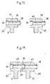
- Fig. 3 is a perspective view showing an outward appearance of a semiconductor device embodying this invention.
- Fig. 4 is a sectional view of the semiconductor device shown in Fig. 3.
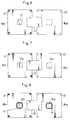
- a semiconductor device 10 has a rectangular package 11.
- the package 11 is about 10 to 50mm long in one side, and about 2 to 8mm thick.
- the package 11 is not limited to the rectangular shape but may be disk-shaped, for example.
- the package 11 encloses at least one semiconductor element. In this embodiment, two semiconductor elements 12a and 12b are enclosed therein.
- the package 11 includes a plurality of exposed terminals 13 for connection to an external, arranged two-dimensionally on a front side surface 11a and a back side surface 11b thereof.
- the exposed terminals 13 are about 0.3 to 1.2mm in diameter, and are arranged at intervals of about 0.5 to 1.5mm.
- the semiconductor elements 12a and 12b and the exposed terminals 13 on opposite surfaces 11a and 11b of package 11 are interconnected through internal wiring such as fine metal lines 14 and multi-layer wiring patterns 15.
- the semiconductor device 10 in this embodiment includes package bases 16a and 16b defining the opposite surfaces 11a and 11b of package 11.
- the package bases 16a and 16b are formed of ceramic, an epoxy resin or the like.
- the exposed terminals 13 are formed on outer surfaces of the package bases 16a and 16b (i.e. the opposite surfaces 11a and 11b of package 11).
- the semiconductor elements 12a and 12b are die-bonded by a conductive epoxy resin or the like to inner surfaces of the package bases 16a and 16b, respectively.
- the package bases 16a and 16b are interconnected inside the package 11 through a flexible printed circuit board 17. A space between the package bases 16a and 16b is filled with an insulating epoxy resin 18, for example.
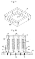
- package bases 16a and 16b defining through holes and multi-layer wiring are prepared.
- the exposed terminals 13 are already formed on the outer surfaces (back side surfaces in Fig. 5) of the package bases 16a and 16b.
- the package bases 16a and 16b define die pads 19 centrally of the inner surfaces thereof, respectively, for die-bonding the semiconductor elements 12a and 12b.
- Ends of a plurality of wiring patterns 15 are arranged around each die pad 19.
- the other ends of wiring patterns 15 are connected to the exposed terminals 13 through the multi-layer wiring and through holes formed in the package bases 16a and 16b. Part of the other ends are connected to internal connection terminals 20 formed on the inner surface adjacent one side of each package base 16a or 16b.
- the flexible printed circuit board 17 defining wiring patterns 17a extends between the internal connection terminals 20 of the two package bases 16a and 16b.
- the package base 16b includes pins 21 erected at the four corners of the inner surface thereof.
- Each pin 21 has a projection 21a formed at a free end thereof.
- the package base 16a defines holes 22 at the four corners of the inner surface thereof for fitting tight with the projections 21a.
- the semiconductor element 12b is die-bonded with a conductive epoxy resin on the die pad 19 of the package base 16b. Further, as shown in Fig. 7, the semiconductor element 12a is likewise die-bonded on the die pad 19 of the package base 16a.
- fine metal lines 14 are formed for wire-bonding between the ends of wiring patterns 15 and bonding pads of the semiconductor element 12b on the package base 16b.
- the semiconductor element 12a on the package base 16a is wire-bonded similarly.
- protective films 23 are formed by potting an insulating epoxy resin or the like over the semiconductor elements 12a and 12b and fine metal lines 14.
- the two package bases 16a and 16b are assembled to extend parallel to each other as vertically spaced by the pins 21, with the holes 22 at the four corners of the package base 16b fitted on the projections 21a of the pins 21 on the package base 16b.
- the assembly is placed in a square frame 24 for use in resin injection.
- the frame 24 is vertically open, and has a supporting shoulder 24a formed around a lower inner surface thereof.
- One side of the frame 24 is perforated to define a resin inlet 24b.
- the two package bases 16a and 16b are placed in the frame 24, with the package base 16b supported at peripheries thereof by the supporting shoulder 24a.
- the space between the package bases 16a and 16b is filled with the insulating epoxy resin 18 introduced through the resin inlet 24b.
- the package 11 is removed from the frame 24 to obtain the semiconductor device 10 shown in Fig. 3.
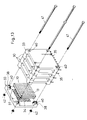
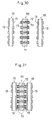
- Fig. 12 is a perspective view of the connectors embodying this invention.
- Fig. 13 is an exploded perspective view showing use of the connectors.
- Figs. 14 and 15 are fragmentary sectional views showing a connector coupling structure.
- Fig. 16 is a front view, partly in section, of the semiconductor devices mounted on a carrier board.
- each connector 30 includes a rectangular base plate 31, and a plurality of connecting pins 32 extending through the base plate 31 to project from opposite surfaces thereof.
- the base plate 31 is formed of an insulating synthetic resin. From the viewpoint of enhanced heat radiation of the connector 30, the base plate 31 may be formed of aluminum and covered with an insulating film.
- the connecting pins 32 are elastic axially thereof. Details of the connecting pins 32 will be described later.
- the connecting pins 32 are arranged two-dimensionally at the intervals corresponding to those of the exposed terminals 13 of the semiconductor device 10. When the semiconductor device 10 is sandwiched between two connectors 30, the connecting pins 32 of the respective connectors 30 press on the exposed terminals 13 on the opposite surfaces of the semiconductor device 10.
- These connecting pins 32 correspond to the conductive connecting elements of this invention.
- such connectors 30 may be interposed between a plurality of semiconductor devices 10 to realize a high-density package of semiconductor devices 10 (four devices in Fig. 13).
- the connecting pins 32 project from the opposite surfaces of each of the three intermediate connectors 30 shown in Fig. 13, since each is flanked by semiconductor devices 10.
- Each end connector 33 has connecting pins 34 projecting from only an inward surface thereof since only the inward surface is opposed to one of the semiconductor devices 10.
- the connectors 30 having the connecting pins 32 projecting from the opposite surfaces thereof may be used at the ends.
- a plurality of terminals 35 for external connection extend from a lower surface of the base plate 31 of each connector 30 or 33. These terminals 35 are electrically connected to wiring patterns formed on a carrier board when a plurality of semiconductor devices 10 are mounted on the carrier board by means of the connectors 30 and 33. The terminals 35 are electrically connected to appropriate connecting pins 32. A specific construction of terminals 35 will be described later.
- the base plate 31 of each connector 30 has a positioning structure for positioning the semiconductor devices 10 such that the exposed terminals 13 of the semiconductor devices 10 register with the connecting pins 32 of the connector 30.
- the positioning structure is in the form of square blocks 36 formed at the four corners of the base plate 31, with a stepped cutout 37 formed in an inward corner of each block 36. The corners of each semiconductor device 10 are fitted into the cutouts 37 to place the exposed terminals 13 in register with the connecting pins 32. Similar cutouts 37 are formed in each end connector 33 also.
- each connector 30 has a coupling structure for rigidly coupling a plurality of connectors 30 in the direction of their thickness, with semiconductor devices 10 sandwiched therebetween.
- each of the four square blocks 36 has a projection 38 formed on one surface thereof, and a recess 39 formed on the opposite surface for receiving the projection 38 of an adjacent connector 30.
- the projection 38 and recess 39 are penetrated by a bore 40.
- Similar projections 38, recesses 39 and bores 40 are formed on each end connector 33 also.
- a plurality of connectors 30 and 33 are coupled with the semiconductor devices 10 sandwiched therebetween, by fitting the projections 38 of one connector 30 into the recesses 39 of an opposed one of the connectors 30.
- bolts 41 are passed through the four bores 40 of each connector 30 or 33, and nuts 42 are screwed thereon to tighten the connectors 30 and 33 together.
- four semiconductor devices 10 are connected. The number of semiconductor devices 10 may of course be varied.
- the connectors 30 and 33 assembled to form a three-dimensional unit with a plurality of semiconductor devices 10 sandwiched therebetween are mounted on a carrier board 43 as shown in Fig. 16.
- the connectors 30 and 33 integrated are fixed to the carrier board 43 by means of L-shaped metal fittings 44 and screws 45, with the external connection terminals 35 soldered to wiring patterns on the carrier board 43.
- this mode of mounting to the carrier board 43 is not limitative.
- the connectors 30 and 33 integrated may be stacked one over the other on the carrier board 43.
- each connecting pin 32 has a conductive tube 46 opening at opposite ends thereof, and conductive contacts 47 mounted in the tube 46 to be movable longitudinally thereof.
- the tube 46 contains a coil spring 48 for outwardly biasing the contacts 47. Under the biasing force of the spring 48, distal ends of the respective contacts 47 project from the end openings of the tube 46.
- the contacts 47 have large diameter proximal ends to prevent the contacts 47 from falling off the tube 46.
- each connecting pin 32 is about 3 to 5mm long, and about 0.6 to 0.7mm in outside diameter.
- Each contact 47 is about 0.2 to 0.3mm in diameter.
- the length of the distal end of each contact 47 projecting from the opening of the tube 46, i.e. a range of movement (or stroke) of each contact 47, is about 0.6 to 0.8mm. With this relatively large range of movement, the contacts 47 may reliably be pressed into contact with the exposed terminals 13 formed on the semiconductor devices 10 even if variations should occur in the height of exposed terminals 13.
- each contact 47 defines a centrally recessed end surface 47a. This shape is selected in order to increase a pressure of elastic contact between the end surface 47a of the contact 47 and one of the exposed terminals 13 formed on semiconductor device 10, to assure an electrical connection therebetween.
- Other desirable shapes of the end surface 47a of each contact 47 are spherical as shown in Fig. 20B, and jagged as shown in Fig. 20C.
- Fig. 19 shows a structure for mounting each connecting pin 32 in the base plate 31 of the connector 30.
- the base plate 31 is formed of two plate members 31a and 31b joined together. Before joining the plate members 31a and 31b, bores are formed therein for receiving the connecting pins 32. The bores are slightly enlarged at openings thereof in opposed mating surfaces of the two plate members 31a and 31b to define stepped structures for fitting with a flange 46a formed on the tube 46 of each connecting pin 32. One end of each connecting pin 32 is inserted into one of the bores of one plate member 31a, and then the other plate member 31b is placed thereon with the other end of the connecting pin 32 extending into one of the bores thereof. An appropriate adhesive is applied to the mating surfaces of the plate members 31a and 31b, to obtain the integrated base plate 31 with the connecting pins 32 fixed in place by the plate members 31a and 31b.
- Fig. 21 shows a connecting pin 34 of each end connector 33.
- each connecting pin 34 has a bottomed tube 49 opening only at one end thereof, and one contact 50 axially movably mounted therein.
- the tube 49 contains a coil spring 51 for biasing the contact 50, so that a distal end of the contact 50 projects from the opening of the tube 49.
- the connecting pin 32 shown in Fig. 19 the connecting pin 34 also is secured to the base plate 31 formed of two plate members joined together. However, in the case of each end connector 33, bores are formed only in the inner plate member for receiving the connecting pins 34.
- the terminals 35 for external connection are connected, such as by welding, to the tubes 46 of the connecting pins 32 beforehand, which are to form a lowermost array in the base plate 31.
- Such integrated connecting pins 32 and terminals 35 are assembled to the base plate 31.
- the terminals 35 for external connection are connected to the tubes 49 of the connecting pins 34 beforehand, which are to form a lowermost array in the base plate 31.
- Such integrated connecting pins 34 and terminals 35 are assembled to the base plate 31.
- connection structures between the terminals 35 for external connection and connecting pins 32 and 34 are not limited to the above example.
- through hole plating is applied to the bore of at least one of the plate members 31a and 31b constituting the base plate 31 as described with reference to Fig. 19.
- Printed circuit patterns are formed on the mating surface of plate member 31a or 31b. One end of each printed circuit pattern is connected to the through hole plating, with the other end of the circuit pattern extending toward the terminal 35. The other end is connected, such as by soldering, to one of the terminals 35.
- the connecting pins 32 and 34 regardless of their positions in the two-dimensional arrangement may be electrically connected to the terminals 35 for external connection.
- the exposed terminals 13 of an adjacent pair of semiconductor devices 10 are interconnected through the connecting pins 32 or 34.
- These connecting pins 32 and 34 are extremely short (about 4 to 6mm) to minimize stray capacitance and parasitic inductance.
- a plurality of semiconductor devices 10 arranged in an opposed relationship readily realize a high-density packaging.
- the connectors 30 and 33 are disconnectable simply by removing the coupling bolts 41 shown in Figs. 13 and 16. Thus, when one of the semiconductor devices 10 should fail, the defective device 10 may be replaced and repackaged with ease.
Abstract
Description
- This invention relates to semiconductor devices with semiconductor elements enclosed in packages, methods of electrically connecting such semiconductor devices, and semiconductor device connectors. In particular, the invention relates to a technique of packaging semiconductor devices in high density.
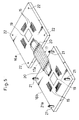
- The development of semiconductor devices has brought about significant increases in the number of terminals (or pins) for external connection. In line with this trend, there exist today multi-terminal semiconductor devices of the types known as QFP (Quad Flat Package) and BGA (Ball Grid Array).
- In QFP, as shown in Fig. 1, a
package 201 has asemiconductor element 202 enclosed therein, andnumerous lead terminals 203 extending from all sides of thepackage 201 for connection to an external. The QFP is mounted on acarrier board 204 with thelead terminals 203 soldered towiring patterns 205. - In BGA, as shown in Fig. 2, a
package 211 has asemiconductor element 212 enclosed therein, andnumerous solder balls 213 arranged two-dimensionally on a back side surface of thepackage 211 for connection to an external. The BGA is mounted on acarrier board 214 with thesolder balls 213 reflow-soldered towiring patterns 215. - However, both QFP and BGA, because each package is mounted in horizontal posture on the surface of the carrier board, have the disadvantage that each semiconductor device occupies a large area of the board. Further, long wiring is required between adjacent semiconductor devices for the same reason. Bus lines are often used to interconnect corresponding terminals of the semiconductor devices. In such a case, a large number of wires longer than one side of each package are required. Long wiring results in marked influences of stray capacitance and parasitic inductance which hamper high-speed processing.
- This invention has been made having regard to the state of the art noted above, and has for a primary object to provide semiconductor devices suited for high-density packaging and for shortening wiring between the semiconductor devices.
- Another object of this invention is to provide a method of connecting such semiconductor devices.
- A further object of this invention is to provide connectors for connecting such semiconductor devices.
- The above primary object is fulfilled, according to this invention, by a semiconductor device comprising:
- a package for enclosing at least one semiconductor element;
- a plurality of exposed terminals for external connection arranged two-dimensionally on each of opposite surfaces of the package; and
- internal wiring for interconnecting the semiconductor element and the exposed terminals for external connection on the opposite surfaces of the package.
- Semiconductor devices according to this invention are assembled three-dimensionally by arranging the devices such that front side surfaces or rear side surfaces of the packages defining the exposed terminals for external connection are in an opposed relationship. The exposed terminals in the opposed relationship of adjacent semiconductor devices are connected to each other. When a plurality of semiconductor devices are mounted on a carrier board, An area of the board occupied by these semiconductor devices corresponds to an installation area where the semiconductor devices assembled three-dimensionally contact the carrier board. This area occupied by the semiconductor devices is far smaller than an area occupied by conventional QFP or BGA devices mounted in horizontal posture on a carrier board. Further, where the exposed terminals of adjacent semiconductor devices are opposed to each other with a small spacing therebetween, only short wirings are required to interconnect the exposed terminals. This provides the advantage of diminishing stray capacitance and parasitic inductance of wirings which hamper high-speed processing.
- Preferably, the package includes package bases defining the opposite surfaces thereof, respectively, the exposed terminals for external connection being formed on outer surfaces of the package bases, the semiconductor element being die-bonded to an inner surface of at least one of the package bases. This construction facilitates fabrication of the semiconductor devices each having exposed terminals arranged on the opposite surfaces of the package.
- A sealing synthetic resin may be filled into a space between the package bases to secure reliability of the semiconductor device.
- Preferably, the package bases are electrically interconnected through a flexible printed circuit board defining a plurality of wiring patterns, the wiring patterns being connected at first ends thereof to internal terminals formed on an inner surface of one of the package bases, and at second ends thereof to internal terminals formed on an inner surface of the other of the package bases. This construction facilitates electrical connection between the two package bases.
- This invention also provides a method of electrically connecting a plurality of semiconductor devices each having at least one semiconductor element enclosed in a package, a plurality of exposed terminals for external connection arranged two-dimensionally on each of opposite surfaces of the package, and internal wiring for interconnecting the semiconductor element and the exposed terminals for external connection on the opposite surfaces of the package, the method comprising:
- arranging the semiconductor devices at fixed intervals with the exposed terminals of one semiconductor device opposed to the exposed terminals of another semiconductor device; and
- interposing conductive connecting elements between an adjacent pair of the semiconductor devices, to interconnect the exposed terminals of one semiconductor device and the exposed terminals of another semiconductor device, thereby to electrically connect the semiconductor devices.
- With the method of connecting semiconductor devices according to this invention, the semiconductor devices are arranged in an opposed relationship and at fixed intervals, with the conductive connecting elements interposed between an adjacent pair of the semiconductor devices to interconnect the exposed terminals of one semiconductor device and the exposed terminals of another semiconductor device. The semiconductor devices assembled in this way occupy only a very small area of a carrier board. Where an adjacent pair of semiconductor devices are arranged close to each other, the conductive connecting elements may have a minimal length for interconnecting the exposed terminals of the two semiconductor devices.
- In the method according to this invention, the conductive connecting elements may, for example, be connecting pins having opposite ends thereof elastically contacting the exposed terminals opposed to each other. Alternatively, the conductive connecting elements may be connecting pins having opposite ends thereof joined by a joining material to the exposed terminals opposed to each other.
- In a further aspect of this invention, there is provided a connector assembly for electrically connecting a plurality of semiconductor devices each having at least one semiconductor element enclosed in a package, a plurality of exposed terminals for external connection arranged two-dimensionally on each of opposite surfaces of the package, and internal wiring for interconnecting the semiconductor element and the exposed terminals for external connection on the opposite surfaces of the package. The connector assembly comprises a plurality of connectors each including:
- a base plate; and
- conductive connecting elements arranged two-dimensionally on the base plate in a corresponding relationship to the exposed terminals, the conductive connecting elements extending through the base plate and projecting from opposite surfaces thereof.
- According to this invention, each connector is interposed between an adjacent pair of semiconductor devices. The base plate has conductive connecting elements in the same arrangement as the exposed terminals of the semiconductor devices. The conductive connecting elements extend through the base plate to project from the opposite surfaces thereof. The exposed terminals of an adjacent pair of semiconductor devices are electrically interconnected through the conductive connecting elements of the connector.
- The semiconductor devices may be assembled in high density by interposing therebetween the connector according to this invention. The conductive connecting elements for electrically interconnecting the exposed terminals of adjacent semiconductor devices may have a minimal length to minimize the influences of stray capacitance and parasitic inductance of wirings (connecting elements) which hamper high-speed processing of the semiconductor devices.
- Preferably, the base plate includes a positioning structure for positioning the semiconductor devices such that the exposed terminals register with the conductive connecting elements. This construction facilitates a positional adjustment between the exposed terminals of the semiconductor devices and the conductive connecting elements of the connector.
- Preferably, the base plate includes external connection terminals arranged on at least one side surface thereof. When the semiconductor devices are mounted on a carrier board by means of the connector assembly, the external connection terminals may be used to facilitate connection to the wiring patterns on the carrier board.
- The conductive connecting elements may, for example, be axially elastic connecting pins having opposite ends thereof elastically contacting the exposed terminals of the semiconductor devices opposed to each other. According to this construction, the connectors and semiconductor devices are only in elastic contact with each other. Any semiconductor device failing to function properly after mounting on a carrier board may be replaced with ease.
- Preferably, the connector assembly further comprises a coupling structure for rigidly coupling the base plates arranged in a direction of thickness thereof, with the semiconductor devices interposed therebetween. This coupling structure assures the elastic contact between the elastic connecting pins and the exposed terminals of the semiconductor devices. Any semiconductor device may be replaced with ease by undoing the coupling structure.
- Preferably, each of the elastic connecting pins includes a conductive tube opening at opposite ends thereof, a pair of conductive contacts disposed in opposite end regions of the tube to be movable longitudinally thereof, the contacts being retained in the tube with only tip ends of the contacts projectable from the opposite ends, respectively, and a biasing element mounted in the tube for biasing the contacts in directions to project the tip ends from the opposite ends.
- The conductive connecting elements may be connecting pins in form of metal rods having opposite ends thereof joined through a joining material to the exposed terminals of the semiconductor devices opposed to each other. Such a connector has a simplified construction, and yet assures the electrical connection between semiconductor device and connector.
- Preferably, the connecting pins in form of metal rods have solder balls formed at opposite ends thereof. Such solder balls may be formed easily by electroplating. This involves a less chance of adversely affecting the semiconductor devices than where solder balls are formed by electroplating on the exposed terminals of the semiconductor devices.
- The conductive connecting elements may be through hole platings formed by plating a metal in bores of the base plate. In this case, the through hole platings have opposite ends thereof joined through a joining material to the exposed terminals of the semiconductor devices opposed to each other.
- For the purpose of illustrating the invention, there are shown in the drawings several forms which are presently preferred, it being understood, however, that the invention is not limited to the precise arrangements and instrumentalities shown.
- Fig. 1 is a perspective view showing one example of conventional semiconductor devices;
- Fig. 2 is a perspective view showing another example of conventional semiconductor devices;
- Fig. 3 is a perspective view showing an outward appearance of a semiconductor device embodying this invention;
- Fig. 4 is a sectional view of the semiconductor device embodying this invention;
- Fig. 5 is a perspective view of package bases used with the semiconductor device;
- Fig. 6 is a plan view showing a semiconductor element fixed to one of the package bases;
- Fig. 7 is a plan view showing semiconductor elements fixed to both of the package bases;
- Fig. 8 is a plan view of the semiconductor elements wire-bonded;
- Fig. 9 is a plan view of the semiconductor elements potted with a resin;
- Figs. 10A and 10B are sectional views showing a process of filling the resin into a space between the package bases;
- Fig. 11 is a perspective view of a frame used in the resin filling process;
- Fig. 12 is a perspective view of connectors embodying this invention;
- Fig. 13 is a perspective view showing a way in which semiconductor devices are assembled with the connectors;
- Fig. 14 is a fragmentary sectional view showing a connector coupling structure;
- Fig. 15 is a fragmentary section view of the connectors in a coupled state;
- Fig. 16 is a front view, partly in section, of the semiconductor devices mounted on a carrier board by means of the connectors;
- Fig. 17 is a front view of a connecting pin;
- Fig. 18 is a sectional view of the connecting pin shown in Fig. 17;
- Fig. 19 is a sectional view showing a structure for mounting a connecting pin;
- Figs. 20A through 20C are sectional views showing varied shapes of an end of the connecting pin;
- Fig. 21 is a sectional view of a connecting pin of an end connector;
- Fig. 22 is a perspective view showing a connection between a connecting pin and an external connection terminal;
- Fig. 23 is a perspective view showing a connection between a connecting pin of an end connector and an external connection terminal;
- Fig. 24 is a fragmentary sectional view showing a modified connector coupling structure;
- Fig. 25 is a fragmentary section view of the connectors of Fig. 24 in a coupled state;
- Fig. 26 is a sectional view of another example of connecting pins;
- Fig. 27 is a sectional view showing a modified structure for mounting a connecting pin;
- Fig. 28 is a sectional view of a modified connector;
- Fig. 29 is a sectional view of the connector of Fig. 28 connected to semiconductor devices;
- Fig. 30 is a sectional view of a further modified connector; and
- Fig. 31 is a sectional view of the connector of Fig. 30 connected to semiconductor devices.
- Semiconductor devices, a method of connecting the semiconductor devices, and semiconductor device connectors in preferred embodiments of this invention will be described hereinafter with reference to the drawings.
- A semiconductor device according to this invention will be described first.
- Fig. 3 is a perspective view showing an outward appearance of a semiconductor device embodying this invention. Fig. 4 is a sectional view of the semiconductor device shown in Fig. 3.
- Referring to Figs. 3 and 4, a
semiconductor device 10 according to this invention has arectangular package 11. Thepackage 11 is about 10 to 50mm long in one side, and about 2 to 8mm thick. Thepackage 11 is not limited to the rectangular shape but may be disk-shaped, for example. Thepackage 11 encloses at least one semiconductor element. In this embodiment, twosemiconductor elements package 11 includes a plurality of exposedterminals 13 for connection to an external, arranged two-dimensionally on afront side surface 11a and aback side surface 11b thereof. The exposedterminals 13 are about 0.3 to 1.2mm in diameter, and are arranged at intervals of about 0.5 to 1.5mm. Thesemiconductor elements terminals 13 onopposite surfaces package 11 are interconnected through internal wiring such asfine metal lines 14 andmulti-layer wiring patterns 15. - The
semiconductor device 10 in this embodiment includespackage bases opposite surfaces package 11. The package bases 16a and 16b are formed of ceramic, an epoxy resin or the like. The exposedterminals 13 are formed on outer surfaces of the package bases 16a and 16b (i.e. theopposite surfaces semiconductor elements package 11 through a flexible printedcircuit board 17. A space between the package bases 16a and 16b is filled with an insulatingepoxy resin 18, for example. - A process of manufacturing the
semiconductor device 10 shown in Figs. 3 and 4 will be described next. - As shown in Fig. 5,
package bases terminals 13 are already formed on the outer surfaces (back side surfaces in Fig. 5) of the package bases 16a and 16b. The package bases 16a and 16b definedie pads 19 centrally of the inner surfaces thereof, respectively, for die-bonding thesemiconductor elements wiring patterns 15 are arranged around each diepad 19. The other ends ofwiring patterns 15 are connected to the exposedterminals 13 through the multi-layer wiring and through holes formed in the package bases 16a and 16b. Part of the other ends are connected tointernal connection terminals 20 formed on the inner surface adjacent one side of eachpackage base circuit board 17 definingwiring patterns 17a extends between theinternal connection terminals 20 of the twopackage bases - The
package base 16b includespins 21 erected at the four corners of the inner surface thereof. Eachpin 21 has aprojection 21a formed at a free end thereof. On the other hand, thepackage base 16a definesholes 22 at the four corners of the inner surface thereof for fitting tight with theprojections 21a. - Subsequently, as shown in Fig. 6, the
semiconductor element 12b is die-bonded with a conductive epoxy resin on thedie pad 19 of thepackage base 16b. Further, as shown in Fig. 7, thesemiconductor element 12a is likewise die-bonded on thedie pad 19 of thepackage base 16a. - Next, as shown in Fig. 8,
fine metal lines 14 are formed for wire-bonding between the ends ofwiring patterns 15 and bonding pads of thesemiconductor element 12b on thepackage base 16b. Thesemiconductor element 12a on thepackage base 16a is wire-bonded similarly. Thereafter, as shown in Fig. 9,protective films 23 are formed by potting an insulating epoxy resin or the like over thesemiconductor elements - After forming the
protective films 23, as shown in Fig. 10A, the twopackage bases pins 21, with theholes 22 at the four corners of thepackage base 16b fitted on theprojections 21a of thepins 21 on thepackage base 16b. The assembly is placed in asquare frame 24 for use in resin injection. As shown in Fig. 11, theframe 24 is vertically open, and has a supportingshoulder 24a formed around a lower inner surface thereof. One side of theframe 24 is perforated to define aresin inlet 24b. The twopackage bases frame 24, with thepackage base 16b supported at peripheries thereof by the supportingshoulder 24a. As shown in Fig. 10B, the space between the package bases 16a and 16b is filled with the insulatingepoxy resin 18 introduced through theresin inlet 24b. Finally, thepackage 11 is removed from theframe 24 to obtain thesemiconductor device 10 shown in Fig. 3. - Next, the method of electrically connecting semiconductor devices as shown in Fig. 3 and the connectors used therein will be described.
- Fig. 12 is a perspective view of the connectors embodying this invention. Fig. 13 is an exploded perspective view showing use of the connectors. Figs. 14 and 15 are fragmentary sectional views showing a connector coupling structure. Fig. 16 is a front view, partly in section, of the semiconductor devices mounted on a carrier board.
- As shown in Fig. 12, each
connector 30 includes arectangular base plate 31, and a plurality of connectingpins 32 extending through thebase plate 31 to project from opposite surfaces thereof. Thebase plate 31 is formed of an insulating synthetic resin. From the viewpoint of enhanced heat radiation of theconnector 30, thebase plate 31 may be formed of aluminum and covered with an insulating film. The connecting pins 32 are elastic axially thereof. Details of the connectingpins 32 will be described later. The connecting pins 32 are arranged two-dimensionally at the intervals corresponding to those of the exposedterminals 13 of thesemiconductor device 10. When thesemiconductor device 10 is sandwiched between twoconnectors 30, the connectingpins 32 of therespective connectors 30 press on the exposedterminals 13 on the opposite surfaces of thesemiconductor device 10. These connectingpins 32 correspond to the conductive connecting elements of this invention. - As shown in Fig. 13,
such connectors 30 may be interposed between a plurality ofsemiconductor devices 10 to realize a high-density package of semiconductor devices 10 (four devices in Fig. 13). The connecting pins 32 project from the opposite surfaces of each of the threeintermediate connectors 30 shown in Fig. 13, since each is flanked bysemiconductor devices 10. Eachend connector 33, on the other hand, has connectingpins 34 projecting from only an inward surface thereof since only the inward surface is opposed to one of thesemiconductor devices 10. Of course, theconnectors 30 having the connectingpins 32 projecting from the opposite surfaces thereof may be used at the ends. - A plurality of
terminals 35 for external connection extend from a lower surface of thebase plate 31 of eachconnector terminals 35 are electrically connected to wiring patterns formed on a carrier board when a plurality ofsemiconductor devices 10 are mounted on the carrier board by means of theconnectors terminals 35 are electrically connected to appropriate connecting pins 32. A specific construction ofterminals 35 will be described later. - The
base plate 31 of eachconnector 30 has a positioning structure for positioning thesemiconductor devices 10 such that the exposedterminals 13 of thesemiconductor devices 10 register with the connectingpins 32 of theconnector 30. Specifically, the positioning structure is in the form ofsquare blocks 36 formed at the four corners of thebase plate 31, with a steppedcutout 37 formed in an inward corner of eachblock 36. The corners of eachsemiconductor device 10 are fitted into thecutouts 37 to place the exposedterminals 13 in register with the connecting pins 32.Similar cutouts 37 are formed in eachend connector 33 also. - The
base plate 31 of eachconnector 30 has a coupling structure for rigidly coupling a plurality ofconnectors 30 in the direction of their thickness, withsemiconductor devices 10 sandwiched therebetween. Specifically, as shown in Fig. 14, each of the foursquare blocks 36 has aprojection 38 formed on one surface thereof, and arecess 39 formed on the opposite surface for receiving theprojection 38 of anadjacent connector 30. Theprojection 38 andrecess 39 are penetrated by abore 40.Similar projections 38, recesses 39 and bores 40 are formed on eachend connector 33 also. - As shown in Fig. 15, a plurality of
connectors semiconductor devices 10 sandwiched therebetween, by fitting theprojections 38 of oneconnector 30 into therecesses 39 of an opposed one of theconnectors 30. After theconnectors bolts 41 are passed through the four bores 40 of eachconnector nuts 42 are screwed thereon to tighten theconnectors semiconductor devices 10 are connected. The number ofsemiconductor devices 10 may of course be varied. - The
connectors semiconductor devices 10 sandwiched therebetween are mounted on acarrier board 43 as shown in Fig. 16. Specifically, theconnectors carrier board 43 by means of L-shapedmetal fittings 44 and screws 45, with theexternal connection terminals 35 soldered to wiring patterns on thecarrier board 43. Of course, this mode of mounting to thecarrier board 43 is not limitative. For example, theconnectors carrier board 43. - The connecting pins 32 arranged two-dimensionally on each
connector 30 will be described next with reference to Figs. 17 through 20. - As shown in Figs. 17 and 18, each connecting
pin 32 has aconductive tube 46 opening at opposite ends thereof, andconductive contacts 47 mounted in thetube 46 to be movable longitudinally thereof. Thetube 46 contains acoil spring 48 for outwardly biasing thecontacts 47. Under the biasing force of thespring 48, distal ends of therespective contacts 47 project from the end openings of thetube 46. Thecontacts 47 have large diameter proximal ends to prevent thecontacts 47 from falling off thetube 46. Thesecontacts 47 of each connectingpin 32 are electrically interconnected through theconductive tube 46 andcoil spring 48. - The
tube 46 of each connectingpin 32 is about 3 to 5mm long, and about 0.6 to 0.7mm in outside diameter. Eachcontact 47 is about 0.2 to 0.3mm in diameter. The length of the distal end of eachcontact 47 projecting from the opening of thetube 46, i.e. a range of movement (or stroke) of eachcontact 47, is about 0.6 to 0.8mm. With this relatively large range of movement, thecontacts 47 may reliably be pressed into contact with the exposedterminals 13 formed on thesemiconductor devices 10 even if variations should occur in the height of exposedterminals 13. - As shown in Fig. 20A, each
contact 47 defines a centrally recessedend surface 47a. This shape is selected in order to increase a pressure of elastic contact between theend surface 47a of thecontact 47 and one of the exposedterminals 13 formed onsemiconductor device 10, to assure an electrical connection therebetween. Other desirable shapes of theend surface 47a of eachcontact 47 are spherical as shown in Fig. 20B, and jagged as shown in Fig. 20C. - Fig. 19 shows a structure for mounting each connecting
pin 32 in thebase plate 31 of theconnector 30. - As seen in Fig. 19, the
base plate 31 is formed of twoplate members plate members plate members flange 46a formed on thetube 46 of each connectingpin 32. One end of each connectingpin 32 is inserted into one of the bores of oneplate member 31a, and then theother plate member 31b is placed thereon with the other end of the connectingpin 32 extending into one of the bores thereof. An appropriate adhesive is applied to the mating surfaces of theplate members integrated base plate 31 with the connectingpins 32 fixed in place by theplate members - Fig. 21 shows a connecting
pin 34 of eachend connector 33. - Such connecting
pins 34 are attached to only one surface of eachend connector 33. Thus, each connectingpin 34 has a bottomedtube 49 opening only at one end thereof, and onecontact 50 axially movably mounted therein. Thetube 49 contains acoil spring 51 for biasing thecontact 50, so that a distal end of thecontact 50 projects from the opening of thetube 49. As is the connectingpin 32 shown in Fig. 19, the connectingpin 34 also is secured to thebase plate 31 formed of two plate members joined together. However, in the case of eachend connector 33, bores are formed only in the inner plate member for receiving the connecting pins 34. - Connection structures between the
terminals 35 for external connection and connectingpins - In the case of
connector 30, as shown in Fig. 22, theterminals 35 for external connection are connected, such as by welding, to thetubes 46 of the connectingpins 32 beforehand, which are to form a lowermost array in thebase plate 31. Such integrated connectingpins 32 andterminals 35 are assembled to thebase plate 31. Similarly, in the case ofend connector 33, as shown in Fig. 23, theterminals 35 for external connection are connected to thetubes 49 of the connectingpins 34 beforehand, which are to form a lowermost array in thebase plate 31. Such integrated connectingpins 34 andterminals 35 are assembled to thebase plate 31. - The connection structures between the
terminals 35 for external connection and connectingpins plate members base plate 31 as described with reference to Fig. 19. Printed circuit patterns are formed on the mating surface ofplate member terminals 35. With this construction, the connectingpins terminals 35 for external connection. - By using the
above connectors semiconductor devices 10, the exposedterminals 13 of an adjacent pair ofsemiconductor devices 10 are interconnected through the connectingpins pins semiconductor devices 10 arranged in an opposed relationship readily realize a high-density packaging. Theconnectors coupling bolts 41 shown in Figs. 13 and 16. Thus, when one of thesemiconductor devices 10 should fail, thedefective device 10 may be replaced and repackaged with ease. - This invention is not limited to the foregoing embodiment, but may be modified as follows:
- (1) In the foregoing embodiment, bolts and nuts are used to couple a plurality of
connectors connector 30 has aprojection 52 on one surface of eachcorner block 36. The other surface of eachcorner block 36 defines ahole 53 accommodating aleaf spring 54 in a tubular form. When theprojection 52 of oneconnector 30 is inserted into thehole 53 of anotherconnector 30, as shown in Fig. 25, agroove 52a of theprojection 52 fits with aridge 54a of theleaf spring 54, thereby coupling the twoconnectors 30. - (2) In the foregoing embodiment, each connecting
pin 32 has a pair ofcontacts 47 biased by acoil spring 48 mounted in atube 46. Instead, thecontacts 47 may be biased by aleaf spring 55 as shown in Fig. 26. - (3) As shown in Fig. 27, the
plate members base plate 31 may have steppedopenings 56 formed in the mating surfaces thereof to be slightly longer than theflange 46a of the connectingpin 32, whereby the entire connectingpin 32 is axially displaceable. With this construction, the connectingpins 32 contacting the exposedterminals 13 of thesemiconductor devices 10 are axially displaceable to follow large variations, if any, in the height of the exposedterminals 13 exceeding the stroke of thecontacts 47. Consequently, the exposedterminals 13 and connectingpins 32 contact each other with increased reliability. - (4) The foregoing embodiment has been described as having axially elastic connecting
pins connector 60 in this example includes abase plate 61 having a two-dimensional arrangement of connectingpins 62 in the form of rod-shaped metal elements. Each connectingpin 62 hassolder balls 63 formed at opposite ends thereof. The solder balls may be formed with ease by electroplating carried out after forming an insulating film on a shank portion, excluding the opposite ends, of the connectingpin 62. The aspects other than the connectingpins 62 are the same as in theconnectors connectors 60 are connected to thesemiconductor devices 10 by what is known as a reflow process. That is, as shown in Fig. 29, the connectingpins 62 of eachconnector 60 placed in contact with the exposedterminals 13 of thesemiconductor devices 10 are heated, whereby thesolder balls 63 are fused to join the exposedterminals 13 and connecting pins 62. Theconnectors 60 in this example have a relatively simple construction and may be manufactured at low cost. The exposedterminals 13 and connectingpins 62 joined with solder have a reliable electrical connection therebetween. - (5) Fig. 30 shows a further example of conductive connecting elements. Each
connector 70 in this example includes abase plate 71 having a two-dimensional arrangement of throughhole platings 72.Solders 73 are formed on each through hole plating 72 by electroplating. As is theconnector 60 shown in Fig. 28, thisconnector 70 also is connected to thesemiconductor devices 10 by a reflow process. Fig. 31 shows a connected state. Theconnectors 70 in this example may also be manufactured at low cost, and the exposedterminals 13 and connectingpins 72 are electrically connected with assurance. - The present invention may be embodied in other specific forms without departing from the spirit or essential attributes thereof and, accordingly, reference should be made to the appended claims, rather than to the foregoing specification, as indicating the scope of the invention.
Claims (16)
- A semiconductor device having at least one semiconductor element enclosed in a package, comprising:package means for enclosing said semiconductor element;a plurality of exposed terminals for external connection arranged two-dimensionally on each of opposite surfaces of said package means; andinternal wiring means for interconnecting said semiconductor element and said exposed terminals for external connection on said opposite surfaces of said package means.
- A semiconductor device as defined in claim 1, wherein said package means includes package bases defining said opposite surfaces thereof, respectively, said exposed terminals for external connection being formed on outer surfaces of said package bases, said semiconductor element being die-bonded to an inner surface of at least one of said package bases.
- A semiconductor device as defined in claim 2, further comprising a sealing synthetic resin filled into a space between said package bases.
- A semiconductor device as defined in claim 2, wherein said package bases are electrically interconnected through a flexible printed circuit board defining a plurality of wiring patterns, said wiring patterns being connected at first ends thereof to internal terminals formed on an inner surface of one of said package bases, and at second ends thereof to internal terminals formed on an inner surface of the other of said package bases.
- A method of electrically connecting a plurality of semiconductor devices each having at least one semiconductor element enclosed in a package, a plurality of exposed terminals for external connection arranged two-dimensionally on each of opposite surfaces of the package, and internal wiring for interconnecting the semiconductor element and the exposed terminals for external connection on the opposite surfaces of the package, said method comprising:arranging said semiconductor devices at fixed intervals with said exposed terminals of one semiconductor device opposed to said exposed terminals of another semiconductor device; andinterposing conductive connecting elements between an adjacent pair of said semiconductor devices, to interconnect said exposed terminals of one semiconductor device and said exposed terminals of another semiconductor device, thereby to electrically connect said semiconductor devices.
- A method as defined in claim 5, wherein said conductive connecting elements are connecting pins having opposite ends thereof elastically contacting said exposed terminals opposed to each other.
- A method as defined in claim 5, wherein said conductive connecting elements are connecting pins having opposite ends thereof joined by a joining material to said exposed terminals opposed to each other.
- A connector assembly for electrically connecting a plurality of semiconductor devices each having at least one semiconductor element enclosed in a package, a plurality of exposed terminals for external connection arranged two-dimensionally on each of opposite surfaces of the package, and internal wiring for interconnecting the semiconductor element and the exposed terminals for external connection on the opposite surfaces of the package, said connector assembly comprising a plurality of connectors each including:a base plate; andconductive connecting elements arranged two-dimensionally on said base plate in a corresponding relationship to said exposed terminals, said conductive connecting elements extending through said base plate and projecting from opposite surfaces thereof.
- A connector assembly as defined in claim 8, wherein said base plate includes a positioning structure for positioning said semiconductor devices such that said exposed terminals register with said conductive connecting elements.
- A connector assembly as defined in claim 8, wherein said base plate includes external connection terminals arranged on at least one side surface thereof.
- A connector assembly as defined in claim 8, wherein said conductive connecting elements are axially elastic connecting pins having opposite ends thereof elastically contacting said exposed terminals of said semiconductor devices opposed to each other.
- A connector assembly as defined in claim 11, further comprising a coupling structure for rigidly coupling the base plates arranged in a direction of thickness thereof, with said semiconductor devices interposed therebetween.
- A connector assembly as defined in claim 11, wherein each of said connecting pins includes:a conductive tube opening at opposite ends thereof;a pair of conductive contacts disposed in opposite end regions of said tube to be movable longitudinally thereof, said contacts being retained in said tube with only tip ends of said contacts projectable from said opposite ends, respectively; anda biasing element mounted in said tube for biasing said contacts in directions to project said tip ends from said opposite ends.
- A connector assembly as defined in claim 8, wherein said conductive connecting elements are connecting pins in form of metal rods having opposite ends thereof joined through a joining material to said exposed terminals of said semiconductor devices opposed to each other.
- A connector assembly as defined in claim 14 wherein said connecting pins have solder balls formed at opposite ends thereof.
- A connector assembly as defined in claim 8, wherein said conductive connecting elements are through hole platings formed by plating a metal in bores of said base plate, said through hole platings having opposite ends thereof joined through a joining material to said exposed terminals of said semiconductor devices opposed to each other.
Applications Claiming Priority (3)
| Application Number | Priority Date | Filing Date | Title |
|---|---|---|---|
| JP11827896 | 1996-04-15 | ||
| JP8118278A JP2987101B2 (en) | 1996-04-15 | 1996-04-15 | Method for connecting semiconductor device and connector for semiconductor device |
| JP118278/96 | 1996-04-15 |
Publications (3)
| Publication Number | Publication Date |
|---|---|
| EP0802566A2 true EP0802566A2 (en) | 1997-10-22 |
| EP0802566A3 EP0802566A3 (en) | 1998-10-28 |
| EP0802566B1 EP0802566B1 (en) | 2004-11-03 |
Family
ID=14732708
Family Applications (1)
| Application Number | Title | Priority Date | Filing Date |
|---|---|---|---|
| EP96110808A Expired - Lifetime EP0802566B1 (en) | 1996-04-15 | 1996-07-04 | Semiconductor devices, method of connecting semiconductor devices, and semiconductor device connectors |
Country Status (4)
| Country | Link |
|---|---|
| US (1) | US5777381A (en) |
| EP (1) | EP0802566B1 (en) |
| JP (1) | JP2987101B2 (en) |
| DE (1) | DE69633775T2 (en) |
Cited By (5)
| Publication number | Priority date | Publication date | Assignee | Title |
|---|---|---|---|---|
| EP0949714A2 (en) * | 1998-04-08 | 1999-10-13 | Thomas & Betts International, Inc. | Board to board interconnect |
| DE19923523A1 (en) * | 1999-05-21 | 2000-11-30 | Siemens Ag | Semiconductor module with stacked chip package |
| EP1556895A2 (en) * | 2002-10-08 | 2005-07-27 | Chippac, Inc. | Semiconductor stacked multi-package module having inverted second package |
| EP1617714A1 (en) * | 2004-07-16 | 2006-01-18 | STMicroelectronics S.A. | Electronic circuit assembly, device comprising such assembly and method for fabricating such device |
| FR2905520A1 (en) * | 2006-09-04 | 2008-03-07 | St Microelectronics Sa | Semiconductor package for containing integrated circuits, has ball placed at periphery and remote from integrated circuit chips and connecting plates, and packaging material filled in space between support plates and drowning chips and ball |
Families Citing this family (25)
| Publication number | Priority date | Publication date | Assignee | Title |
|---|---|---|---|---|
| US6284566B1 (en) * | 1996-05-17 | 2001-09-04 | National Semiconductor Corporation | Chip scale package and method for manufacture thereof |
| JP3638771B2 (en) * | 1997-12-22 | 2005-04-13 | 沖電気工業株式会社 | Semiconductor device |
| US6208019B1 (en) * | 1998-03-13 | 2001-03-27 | Kabushiki Kaisha Toshiba | Ultra-thin card-type semiconductor device having an embredded semiconductor element in a space provided therein |
| TW368707B (en) * | 1998-10-27 | 1999-09-01 | Tech Field Co Ltd | Packaging method for semiconductor die and the product of the same |
| US6265771B1 (en) * | 1999-01-27 | 2001-07-24 | International Business Machines Corporation | Dual chip with heat sink |
| JP2003518759A (en) | 1999-12-20 | 2003-06-10 | シンクォール・インコーポレーテッド | Terminal pin with flange for DC / DC converter |
| US7085146B2 (en) * | 1999-12-20 | 2006-08-01 | Synqor, Inc. | Flanged terminal pins for DC/DC converters |
| US6319418B1 (en) | 1999-12-20 | 2001-11-20 | St. Assembly Test Services Pte Ltd. | Zig-zagged plating bus lines |
| US6896526B2 (en) | 1999-12-20 | 2005-05-24 | Synqor, Inc. | Flanged terminal pins for DC/DC converters |
| US20040173106A1 (en) * | 2003-03-03 | 2004-09-09 | Jean Rouleau | Pneumatically driven wringer for use on an open barrell |
| US6853202B1 (en) * | 2002-01-23 | 2005-02-08 | Cypress Semiconductor Corporation | Non-stick detection method and mechanism for array molded laminate packages |
| TW200302685A (en) | 2002-01-23 | 2003-08-01 | Matsushita Electric Ind Co Ltd | Circuit component built-in module and method of manufacturing the same |
| US7349225B1 (en) * | 2002-10-22 | 2008-03-25 | Odyssian Technology, Llc | Multifunctional composite sandwich element with embedded electronics |
| JP2006203086A (en) * | 2005-01-24 | 2006-08-03 | Citizen Electronics Co Ltd | Electronic part package and manufacturing method thereof |
| WO2006080082A1 (en) * | 2005-01-28 | 2006-08-03 | Spansion Llc | Layered semiconductor device carrier and layered semiconductor device manufacturing method |
| US7675151B1 (en) * | 2005-06-01 | 2010-03-09 | Rockwell Collins, Inc. | Silicon-based packaging for electronic devices |
| KR100761468B1 (en) * | 2006-07-13 | 2007-09-27 | 삼성전자주식회사 | Semiconductor device and method of forming the same |
| US20080191367A1 (en) * | 2007-02-08 | 2008-08-14 | Stats Chippac, Ltd. | Semiconductor package wire bonding |
| JP4952365B2 (en) * | 2007-05-07 | 2012-06-13 | 富士通株式会社 | Electronic component mounting structure on a double-sided mounting circuit board, semiconductor device, and manufacturing method of double-sided mounting semiconductor device |
| US8763298B2 (en) | 2008-09-27 | 2014-07-01 | Shane Smith | Combination brush and jag |
| US8146284B2 (en) | 2008-09-27 | 2012-04-03 | Shane Patrick Smith | Combination brush and jag with patch |
| JP6109013B2 (en) * | 2013-08-27 | 2017-04-05 | 三菱電機株式会社 | Semiconductor socket and semiconductor module |
| KR102374430B1 (en) * | 2015-10-08 | 2022-03-15 | 삼성전자주식회사 | Support frame for substrate and storage device having the same |
| US10667396B2 (en) | 2017-08-25 | 2020-05-26 | Tactotek Oy | Multilayer structure for hosting electronics and related method of manufacture |
| TWI687986B (en) * | 2018-11-16 | 2020-03-11 | 典琦科技股份有限公司 | Method for manufacturing chip package |
Citations (7)
| Publication number | Priority date | Publication date | Assignee | Title |
|---|---|---|---|---|
| US4709300A (en) * | 1986-05-05 | 1987-11-24 | Itt Gallium Arsenide Technology Center, A Division Of Itt Corporation | Jumper for a semiconductor assembly |
| EP0284820A2 (en) * | 1987-03-04 | 1988-10-05 | Canon Kabushiki Kaisha | Electrically connecting member, and electric circuit member and electric circuit device with the connecting member |
| EP0535479A1 (en) * | 1991-09-30 | 1993-04-07 | International Business Machines Corporation | Multichip integrated circuit packages and systems |
| US5295044A (en) * | 1991-09-26 | 1994-03-15 | Kabushiki Kaisah Toshiba | Semiconductor device |
| US5321884A (en) * | 1992-01-22 | 1994-06-21 | International Business Machines Corporation | Multilayered flexible circuit package |
| US5382829A (en) * | 1992-07-21 | 1995-01-17 | Mitsubishi Denki Kabushiki Kaisha | Packaged microwave semiconductor device |
| US5383269A (en) * | 1991-09-03 | 1995-01-24 | Microelectronics And Computer Technology Corporation | Method of making three dimensional integrated circuit interconnect module |
Family Cites Families (2)
| Publication number | Priority date | Publication date | Assignee | Title |
|---|---|---|---|---|
| JP3280394B2 (en) * | 1990-04-05 | 2002-05-13 | ロックヒード マーティン コーポレーション | Electronic equipment |
| US5241456A (en) * | 1990-07-02 | 1993-08-31 | General Electric Company | Compact high density interconnect structure |
-
1996
- 1996-04-15 JP JP8118278A patent/JP2987101B2/en not_active Expired - Fee Related
- 1996-06-27 US US08/671,371 patent/US5777381A/en not_active Expired - Fee Related
- 1996-07-04 DE DE69633775T patent/DE69633775T2/en not_active Expired - Fee Related
- 1996-07-04 EP EP96110808A patent/EP0802566B1/en not_active Expired - Lifetime
Patent Citations (7)
| Publication number | Priority date | Publication date | Assignee | Title |
|---|---|---|---|---|
| US4709300A (en) * | 1986-05-05 | 1987-11-24 | Itt Gallium Arsenide Technology Center, A Division Of Itt Corporation | Jumper for a semiconductor assembly |
| EP0284820A2 (en) * | 1987-03-04 | 1988-10-05 | Canon Kabushiki Kaisha | Electrically connecting member, and electric circuit member and electric circuit device with the connecting member |
| US5383269A (en) * | 1991-09-03 | 1995-01-24 | Microelectronics And Computer Technology Corporation | Method of making three dimensional integrated circuit interconnect module |
| US5295044A (en) * | 1991-09-26 | 1994-03-15 | Kabushiki Kaisah Toshiba | Semiconductor device |
| EP0535479A1 (en) * | 1991-09-30 | 1993-04-07 | International Business Machines Corporation | Multichip integrated circuit packages and systems |
| US5321884A (en) * | 1992-01-22 | 1994-06-21 | International Business Machines Corporation | Multilayered flexible circuit package |
| US5382829A (en) * | 1992-07-21 | 1995-01-17 | Mitsubishi Denki Kabushiki Kaisha | Packaged microwave semiconductor device |
Cited By (10)
| Publication number | Priority date | Publication date | Assignee | Title |
|---|---|---|---|---|
| EP0949714A2 (en) * | 1998-04-08 | 1999-10-13 | Thomas & Betts International, Inc. | Board to board interconnect |
| EP0949714A3 (en) * | 1998-04-08 | 2000-11-02 | Thomas & Betts International, Inc. | Board to board interconnect |
| DE19923523A1 (en) * | 1999-05-21 | 2000-11-30 | Siemens Ag | Semiconductor module with stacked chip package |
| US6646333B1 (en) | 1999-05-21 | 2003-11-11 | Infineon Technologies Ag | Semiconductor module having interconnected semiconductor chips disposed one above the other |
| DE19923523B4 (en) * | 1999-05-21 | 2004-09-30 | Infineon Technologies Ag | Semiconductor module with semiconductor chips arranged one above the other and connected to one another |
| EP1556895A2 (en) * | 2002-10-08 | 2005-07-27 | Chippac, Inc. | Semiconductor stacked multi-package module having inverted second package |
| EP1556895A4 (en) * | 2002-10-08 | 2009-12-30 | Chippac Inc | Semiconductor stacked multi-package module having inverted second package |
| EP1617714A1 (en) * | 2004-07-16 | 2006-01-18 | STMicroelectronics S.A. | Electronic circuit assembly, device comprising such assembly and method for fabricating such device |
| WO2006008189A1 (en) * | 2004-07-16 | 2006-01-26 | Stmicroelectronics Sa | Electronic circuit assembly, device comprising such assembly and method for fabricating such device |
| FR2905520A1 (en) * | 2006-09-04 | 2008-03-07 | St Microelectronics Sa | Semiconductor package for containing integrated circuits, has ball placed at periphery and remote from integrated circuit chips and connecting plates, and packaging material filled in space between support plates and drowning chips and ball |
Also Published As
| Publication number | Publication date |
|---|---|
| DE69633775T2 (en) | 2005-11-03 |
| JPH09283698A (en) | 1997-10-31 |
| EP0802566B1 (en) | 2004-11-03 |
| US5777381A (en) | 1998-07-07 |
| EP0802566A3 (en) | 1998-10-28 |
| JP2987101B2 (en) | 1999-12-06 |
| DE69633775D1 (en) | 2004-12-09 |
Similar Documents
| Publication | Publication Date | Title |
|---|---|---|
| US5777381A (en) | Semiconductor devices method of connecting semiconductor devices and semiconductor device connectors | |
| US11700692B2 (en) | Stackable via package and method | |
| JP2967344B2 (en) | Stacked semiconductor package module and manufacturing method of stacked semiconductor package module | |
| US5661339A (en) | Thin multichip module | |
| US6521984B2 (en) | Semiconductor module with semiconductor devices attached to upper and lower surface of a semiconductor substrate | |
| US6617695B1 (en) | Semiconductor device and semiconductor module using the same | |
| KR0127873B1 (en) | Edge-mounted surface-mount package for semiconductor integrated circuit device in tergrateles | |
| US5247423A (en) | Stacking three dimensional leadless multi-chip module and method for making the same | |
| US5942795A (en) | Leaded substrate carrier for integrated circuit device and leaded substrate carrier device assembly | |
| US7038315B2 (en) | Semiconductor chip package | |
| US5045914A (en) | Plastic pad array electronic AC device | |
| US4916523A (en) | Electrical connections via unidirectional conductive elastomer for pin carrier outside lead bond | |
| US5438481A (en) | Molded-in lead frames | |
| JP3137977B2 (en) | Semiconductor device having many lead bins | |
| KR20010078712A (en) | Chip stack and method of making same | |
| JP2007294993A (en) | Assembling type semiconductor chip carrier | |
| JPH06268101A (en) | Semiconductor device and its manufacture, electronic device, lead frame, and mounting substrate | |
| KR970030716A (en) | Three-dimensional stacked package with vertical connecting means formed inside the package | |
| US6992395B2 (en) | Semiconductor device and semiconductor module having external electrodes on an outer periphery | |
| JP2000294720A (en) | Semiconductor integrated circuit package | |
| US4994896A (en) | Semiconductor device | |
| US5062802A (en) | Contact module for a low height multi-chip carrier socket | |
| US6328577B1 (en) | High density electric connector set | |
| JPH04280696A (en) | High integrated semiconductor device | |
| JPS6379361A (en) | Upright installation type semiconductor device |
Legal Events
| Date | Code | Title | Description |
|---|---|---|---|
| PUAI | Public reference made under article 153(3) epc to a published international application that has entered the european phase |
Free format text: ORIGINAL CODE: 0009012 |
|
| AK | Designated contracting states |
Kind code of ref document: A2 Designated state(s): DE FR GB IT NL SE |
|
| PUAL | Search report despatched |
Free format text: ORIGINAL CODE: 0009013 |
|
| AK | Designated contracting states |
Kind code of ref document: A3 Designated state(s): DE FR GB IT NL SE |
|
| 17P | Request for examination filed |
Effective date: 19990126 |
|
| 17Q | First examination report despatched |
Effective date: 20030219 |
|
| GRAP | Despatch of communication of intention to grant a patent |
Free format text: ORIGINAL CODE: EPIDOSNIGR1 |
|
| GRAS | Grant fee paid |
Free format text: ORIGINAL CODE: EPIDOSNIGR3 |
|
| RTI1 | Title (correction) |
Free format text: SEMICONDUCTOR DEVICES, METHOD OF CONNECTING SEMICONDUCTOR DEVICES, AND SEMICONDUCTOR DEVICE CONNECTORS |
|
| GRAA | (expected) grant |
Free format text: ORIGINAL CODE: 0009210 |
|
| AK | Designated contracting states |
Kind code of ref document: B1 Designated state(s): DE FR GB IT NL SE |
|
| REG | Reference to a national code |
Ref country code: GB Ref legal event code: FG4D |
|
| REG | Reference to a national code |
Ref country code: SE Ref legal event code: TRGR |
|
| REF | Corresponds to: |
Ref document number: 69633775 Country of ref document: DE Date of ref document: 20041209 Kind code of ref document: P |
|
| PLBE | No opposition filed within time limit |
Free format text: ORIGINAL CODE: 0009261 |
|
| STAA | Information on the status of an ep patent application or granted ep patent |
Free format text: STATUS: NO OPPOSITION FILED WITHIN TIME LIMIT |
|
| ET | Fr: translation filed | ||
| 26N | No opposition filed |
Effective date: 20050804 |
|
| PGFP | Annual fee paid to national office [announced via postgrant information from national office to epo] |
Ref country code: DE Payment date: 20070908 Year of fee payment: 12 |
|
| PGFP | Annual fee paid to national office [announced via postgrant information from national office to epo] |
Ref country code: GB Payment date: 20070704 Year of fee payment: 12 |
|
| PGFP | Annual fee paid to national office [announced via postgrant information from national office to epo] |
Ref country code: SE Payment date: 20070705 Year of fee payment: 12 Ref country code: NL Payment date: 20070731 Year of fee payment: 12 |
|
| PGFP | Annual fee paid to national office [announced via postgrant information from national office to epo] |
Ref country code: FR Payment date: 20070731 Year of fee payment: 12 |
|
| EUG | Se: european patent has lapsed | ||
| GBPC | Gb: european patent ceased through non-payment of renewal fee |
Effective date: 20080704 |
|
| NLV4 | Nl: lapsed or anulled due to non-payment of the annual fee |
Effective date: 20090201 |
|
| PG25 | Lapsed in a contracting state [announced via postgrant information from national office to epo] |
Ref country code: DE Free format text: LAPSE BECAUSE OF NON-PAYMENT OF DUE FEES Effective date: 20090203 |
|
| REG | Reference to a national code |
Ref country code: FR Ref legal event code: ST Effective date: 20090331 |
|
| PG25 | Lapsed in a contracting state [announced via postgrant information from national office to epo] |
Ref country code: NL Free format text: LAPSE BECAUSE OF NON-PAYMENT OF DUE FEES Effective date: 20090201 |
|
| PG25 | Lapsed in a contracting state [announced via postgrant information from national office to epo] |
Ref country code: GB Free format text: LAPSE BECAUSE OF NON-PAYMENT OF DUE FEES Effective date: 20080704 |
|
| PG25 | Lapsed in a contracting state [announced via postgrant information from national office to epo] |
Ref country code: FR Free format text: LAPSE BECAUSE OF NON-PAYMENT OF DUE FEES Effective date: 20080731 |
|
| PG25 | Lapsed in a contracting state [announced via postgrant information from national office to epo] |
Ref country code: IT Free format text: LAPSE BECAUSE OF NON-PAYMENT OF DUE FEES Effective date: 20070704 |
|
| PG25 | Lapsed in a contracting state [announced via postgrant information from national office to epo] |
Ref country code: SE Free format text: LAPSE BECAUSE OF NON-PAYMENT OF DUE FEES Effective date: 20080705 |
|
| PGFP | Annual fee paid to national office [announced via postgrant information from national office to epo] |
Ref country code: IT Payment date: 20070731 Year of fee payment: 12 |
|
| PGRI | Patent reinstated in contracting state [announced from national office to epo] |
Ref country code: IT Effective date: 20110616 |
|
| PGRI | Patent reinstated in contracting state [announced from national office to epo] |
Ref country code: IT Effective date: 20110616 |